ICS840004I-01
FEMTOCLOCK™ CRYSTAL-TO-LVCMOS/LVTTL
FREQUENCY SYNTHESIZER
General Description
Features
The ICS840004I-01 is a 4 output LVCMOS/LVTTL
Synthesizer optimized to generate Ethernet
HiPerClockS™
reference clock frequencies and is a member of the
HiPerClocksTM family of high performance clock
solutions from IDT. Using a 25MHz, 18pF parallel
resonant crystal, the following frequencies can be generated
based on the 2 frequency select pins (F_SEL1:0): 156.25MHz,
125MHz, and 62.5MHz. The ICS840004I-01 uses IDT’s 3rd
generation low phase noise VCO technology and can achieve 1ps
or lower typical random rms phase jitter, easily meeting Ethernet
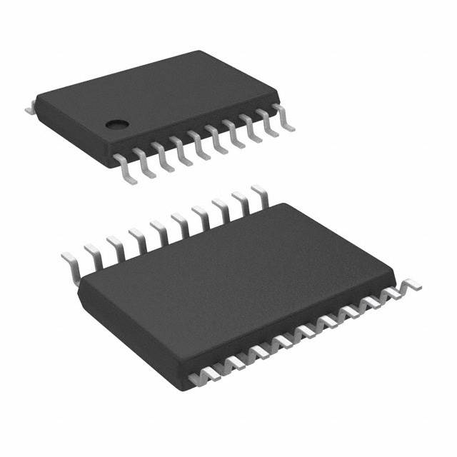
jitter requirements. The ICS840004I-01 is packaged in a small
20-pin TSSOP package.
•
Four single-ended LVCMOS/LVTTL outputs
17Ω typical output impedance
•
Selectable crystal oscillator interface or single-ended input,
Supports the following output frequencies: 156.25MHz,
125MHz and 62.5MHz
•
•
VCO range: 560MHz - 700MHz
•
Output supply modes:
Core/Output
3.3V/3.3V
3.3V/2.5V
2.5V/2.5V
•
•
-40°C to 85°C ambient operating temperature
ICS
RMS phase jitter at 156.25MHz (1.875MHz – 20MHz):
0.52ps (typical)
Available in both standard (RoHS 5) and lead-free (RoHS 6)
packages
Frequency Select Function Table for Ethernet Frequencies
Inputs
F_SEL1
F_SEL0
M Div. Value
N Div. Value
M/N Ratio Value
Output Frequency (MHz), (25MHz Reference)
0
0
25
4
6.25
156.25
0
1
25
5
5
125
1
0
25
10
2.5
62.5
1
1
25
5
5
125 (default)
Pin Assignment
Block Diagram
OE
F_SEL1:0
Pullup
nPLL_SEL
Pulldown
nXTAL_SEL
Pulldown
F_SEL0
nc
nXTAL_SEL
REF_CLK
2
Pullup:Pullup
25MHz
XTAL_IN
OSC
F_SEL1:0
0
1
XTAL_OUT
REF_CLK
Pulldown
1
Phase
Detector
VCO
0
00
01
10
11
N
÷4
÷5
÷10
÷5 (default)
Q0
Q1
Q2
M = ÷25 (fixed)
MR
Q3
OE
MR
nPLL_SEL
VDDA
nc
VDD
1
2
3
4
5
6
7
8
9
10
20
19
18
17
16
15
14
13
12
11
F_SEL1
GND
Q0
Q1
VDDO
Q2
Q3
GND
XTAL_IN
XTAL_OUT
ICS840004I-01
20-Lead TSSOP
6.5mm x 4.4mm x 0.925mm
package body
G Package
Top View
Pulldown
IDT™ / ICS™ LVCMOS/LVTTL FREQUENCY SYNTHESIZER
1
ICS840004AGI-01 REV. B OCTOBER 31, 2008
�ICS840004I-01
FEMTOCLOCKS™ CRYSTAL-TO-LVCMOS/LVTTL CLOCK SYNTHESIZER
Table 1. Pin Descriptions
Number
Name
Type
Description
1, 20
F_SEL0,
F_SEL1
Input
2, 9
nc
Unused
3
nXTAL_SEL
Input
Pulldown
Selects betweent he crystal or REF_CLK inputs as the PLL reference
source. When HIGH, selects REF_CLK. When LOW, selects XTAL
inputs. LVCMOS/LVTTL interface levels.
4
REF_CLK
Input
Pulldown
Single-ended reference clock input. LVCMOS/LVTTL interface levels.
5
OE
Input
Pullup
Output enable pin. When HIGH, the outputs are active. When LOW, the
outputs are in a high impedance state. LVCMOS/LVTTL interface levels.
6
MR
Input
Pulldown
Active HIGH master reset. When logic HIGH, the internal dividers are
reset causing the outputs to go low. When logic LOW, the internal
dividers and the outputs are enabled. LVCMOS/LVTTL interface levels.
7
nPLL_SEL
Input
Pulldown
PLL bypass. When LOW, the output is driven from the VCO output.
When HIGH, the PLL is bypassed and the output frequency = reference
clock frequency/N output divider. LVCMOS/LVTTL interface levels.
8
VDDA
Power
Analog supply pin.
10
VDD
Power
Core supply pin.
11,
12
XTAL_OUT,
XTAL_IN
Input
Crystal oscillator interface. XTAL_IN is the input. XTAL_OUT is the
output.
13, 19
GND
Power
Power supply ground.
14, 15, 17, 18
Q3, Q2, Q1, Q0
Output
Single-ended clock outputs. 17Ω typical output impedance.
LVCMOS/ LVTTL interface levels.
16
VDDO
Power
Output supply pin.
Pullup
Frequency select pins. LVCMOS/LVTTL interface levels.
No connect.
NOTE: Pullup and Pulldown refer to internal input resistors. See Table 2, Pin Characteristics, for typical values.
Table 2. Pin Characteristics
Symbol
Parameter
CIN
Input Capacitance
4
pF
CPD
Power Dissipation Capacitance
8
pF
RPULLUP
Input Pullup Resistor
51
kΩ
RPULLDOWN
Input Pulldown Resistor
51
kΩ
Output Impedance
VDDO = 3.3V±5%
17
ROUT
Ω
VDDO = 2.5V±5%
21
Ω
IDT™ / ICS™ LVCMOS/LVTTL FREQUENCY SYNTHESIZER
Test Conditions
2
Minimum
Typical
Maximum
Units
ICS840004AGI-01 REV. B OCTOBER 31, 2008
�ICS840004I-01
FEMTOCLOCKS™ CRYSTAL-TO-LVCMOS/LVTTL CLOCK SYNTHESIZER
Absolute Maximum Ratings
NOTE: Stresses beyond those listed under Absolute Maximum Ratings may cause permanent damage to the device.
These ratings are stress specifications only. Functional operation of product at these conditions or any conditions beyond
those listed in the DC Characteristics or AC Characteristics is not implied. Exposure to absolute maximum rating conditions for
extended periods may affect product reliability.
Item
Rating
Supply Voltage, VDD
4.6V
Inputs, VI
-0.5V to VDD + 0.5V
Outputs, VO
-0.5V to VDDO + 0.5V
Package Thermal Impedance, θJA
73.2°C/W (0 lfpm)
Storage Temperature, TSTG
-65°C to 150°C
DC Electrical Characteristics
Table 3A. Power Supply DC Characteristics, VDD = 3.3V ± 5%, VDDO = 3.3V ± 5% or 2.5V ± 5%, TA = -40°C to 85°C
Symbol
Parameter
VDD
Test Conditions
Minimum
Typical
Maximum
Units
Core Supply Voltage
3.135
3.3
3.465
V
VDDA
Analog Supply Voltage
3.135
3.3
3.465
V
3.135
3.3
3.465
V
VDDO
Output Supply Voltage
2.375
2.5
2.625
V
IDD
Power Supply Current
100
mA
IDDA
Analog Supply Current
12
mA
IDDO
Output Supply Current
10
mA
Table 3B. Power Supply DC Characteristics, VDD = 2.5V ± 5%, VDDO = 2.5V ± 5%, TA = -40°C to 85°C
Symbol
Parameter
VDD
Test Conditions
Minimum
Typical
Maximum
Units
Core Supply Voltage
2.375
2.5
2.625
V
VDDA
Analog Supply Voltage
2.375
2.5
2.625
V
VDDO
Output Supply Voltage
2.375
2.5
2.625
V
IDD
Power Supply Current
95
mA
IDDA
Analog Supply Current
12
mA
IDDO
Output Supply Current
8
mA
IDT™ / ICS™ LVCMOS/LVTTL FREQUENCY SYNTHESIZER
3
ICS840004AGI-01 REV. B OCTOBER 31, 2008
�ICS840004I-01
FEMTOCLOCKS™ CRYSTAL-TO-LVCMOS/LVTTL CLOCK SYNTHESIZER
Table 3C. LVCMOS/LVTTL DC Characteristics, TA = -40°C to 85°C
Symbol
Parameter
VIH
Input High Voltage
VIL
Input Low Voltage
IIH
IIL
Input
High Current
Input
Low Current
Test Conditions
Minimum
VDD = 3.465V
Typical
Maximum
Units
2
VDD + 0.3
V
VDD = 2.625V
1.7
VDD + 0.3
V
VDD = 3.465V
-0.3
0.8
V
VDD = 2.625V
-0.3
0.7
V
nXTAL_SEL,
nPLL_SEL,
REF_CLK, MR
VDD = VIN = 3.465V or 2.625V
150
µA
OE, F_SEL[0:1]
VDD = VIN = 3.465V or 2.625V
5
µA
nXTAL_SEL,
nPLL_SEL,
REF_CLK, MR
VDD = 3.465V or 2.625V, VIN = 0V
-5
µA
OE, F_SEL[0:1]
VDD = 3.465V or 2.625V, VIN = 0V
-150
µA
VDDO = 3.3V ± 5%
2.6
V
VDDO = 2.5V ± 5%
1.8
V
VOH
Output High Voltage; NOTE 1
VOL
Output Low Voltage; NOTE 1
VDDO = 3.3V ± 5% or 2.5V ± 5%
0.5
V
NOTE 1: Outputs terminated with 50Ω to VDDO/2. See Parameter Measurement Information section. Load Test Circuit diagrams.
Table 4. Crystal Characteristics
Parameter
Test Conditions
Mode of Oscillation
Minimum
Typical
Maximum
Units
Fundamental
Frequency
25
MHz
Equivalent Series Resistance (ESR)
50
Ω
Shunt Capacitance
7
pF
Drive Level
1
mW
IDT™ / ICS™ LVCMOS/LVTTL FREQUENCY SYNTHESIZER
4
ICS840004AGI-01 REV. B OCTOBER 31, 2008
�ICS840004I-01
FEMTOCLOCKS™ CRYSTAL-TO-LVCMOS/LVTTL CLOCK SYNTHESIZER
AC Electrical Characteristics
Table 5A. AC Characteristics, VDD = VDDO = 3.3V ± 5%, TA = -40°C to 85°C
Parameter
Symbol
fout
Output Frequency
tsk(o)
Output Skew: NOTE 1, 2
tjit(Ø)
tR / tF
odc
RMS Phase Jitter (Random);
NOTE 3
Test Conditions
Minimum
Typical
Maximum
Units
F_SEL[1:0] = 00
140
156.25
175
MHz
F_SEL[1:0] = 01 or 11
112
125
140
MHz
F_SEL[1:0] = 10
56
62.5
70
MHz
60
MHz
156.25MHz, Integration Range:
1.875MHz – 20MHz
0.52
ps
125MHz, Integration Range:
1.875MHz – 20MHz
0.65
ps
62.5MHz, Integration Range:
1.875MHz – 20MHz
0.55
ps
Output Rise/Fall Time
Output Duty Cycle
20% to 80%
200
700
ps
F_SEL[1:0] = 00, 01 or 11
43
57
%
F_SEL[1:0] = 10
49
51
%
NOTE: Electrical parameters are guaranteed over the specified ambient operating temperature range, which is established when the
device is mounted in a test socket with maintained transverse airflow greater than 500 lfpm. The device will meet specifications after
thermal equilibrium has been reached under these conditions.
NOTE 1: Defined as skew between outputs at the same supply voltage and with equal load conditions. Measured at VDDO/2.
NOTE 2: This parameter is defined in accordance with JEDEC Standard 65.
NOTE 3: Please refer to the Phase Noise Plot.
Table 5B. AC Characteristics, VDD = 3.3V ± 5%, VDDO = 2.5V ± 5%, TA = -40°C to 85°C
Parameter
Symbol
fout
Output Frequency
tsk(o)
Output Skew: NOTE 1, 2
tjit(Ø)
tR / tF
odc
RMS Phase Jitter (Random);
NOTE 3
Test Conditions
Minimum
Typical
Maximum
Units
F_SEL[1:0] = 00
140
156.25
175
MHz
F_SEL[1:0] = 01 or 11
112
125
140
MHz
F_SEL[1:0] = 10
56
62.5
70
MHz
60
MHz
156.25MHz, Integration Range:
1.875MHz – 20MHz
0.48
ps
125MHz, Integration Range:
1.875MHz – 20MHz
0.59
ps
62.5MHz, Integration Range:
1.875MHz – 20MHz
0.53
ps
Output Rise/Fall Time
Output Duty Cycle
20% to 80%
200
700
ps
F_SEL[1:0] = 00, 01 or 11
43
57
%
F_SEL[1:0] = 10
49
51
%
NOTE: Electrical parameters are guaranteed over the specified ambient operating temperature range, which is established when the
device is mounted in a test socket with maintained transverse airflow greater than 500 lfpm. The device will meet specifications after
thermal equilibrium has been reached under these conditions.
NOTE 1: Defined as skew between outputs at the same supply voltage and with equal load conditions. Measured at VDDO/2.
NOTE 2: This parameter is defined in accordance with JEDEC Standard 65.
NOTE 3: Please refer to the Phase Noise Plot.
IDT™ / ICS™ LVCMOS/LVTTL FREQUENCY SYNTHESIZER
5
ICS840004AGI-01 REV. B OCTOBER 31, 2008
�ICS840004I-01
FEMTOCLOCKS™ CRYSTAL-TO-LVCMOS/LVTTL CLOCK SYNTHESIZER
Table 5C. AC Characteristics, VDD = VDDO = 2.5V ± 5%, TA = -40°C to 85°C
Parameter
Symbol
fout
Output Frequency
tsk(o)
Output Skew: NOTE 1, 2
tjit(Ø)
tR / tF
odc
RMS Phase Jitter (Random);
NOTE 3
Test Conditions
Minimum
Typical
Maximum
Units
F_SEL[1:0] = 00
140
156.25
175
MHz
F_SEL[1:0] = 01 or 11
112
125
140
MHz
F_SEL[1:0] = 10
56
62.5
70
MHz
60
MHz
156.25MHz, Integration Range:
1.875MHz – 20MHz
0.50
ps
125MHz, Integration Range:
1.875MHz – 20MHz
0.60
ps
62.5MHz, Integration Range:
1.875MHz – 20MHz
0.51
ps
Output Rise/Fall Time
Output Duty Cycle
20% to 80%
200
700
ps
F_SEL[1:0] = 00, 01 or 11
44
56
%
F_SEL[1:0] = 10
49
51
%
NOTE: Electrical parameters are guaranteed over the specified ambient operating temperature range, which is established when the
device is mounted in a test socket with maintained transverse airflow greater than 500 lfpm. The device will meet specifications after
thermal equilibrium has been reached under these conditions.
NOTE 1: Defined as skew between outputs at the same supply voltage and with equal load conditions. Measured at VDDO/2.
NOTE 2: This parameter is defined in accordance with JEDEC Standard 65.
NOTE 3: Please refer to the Phase Noise Plot.
IDT™ / ICS™ LVCMOS/LVTTL FREQUENCY SYNTHESIZER
6
ICS840004AGI-01 REV. B OCTOBER 31, 2008
�ICS840004I-01
FEMTOCLOCKS™ CRYSTAL-TO-LVCMOS/LVTTL CLOCK SYNTHESIZER
➝
Typical Phase Noise at 62.5MHz (3.3V)
10Gb Ethernet Filter
Raw Phase Noise Data
➝
➝
Noise Power
dBc
Hz
62.5MHz
RMS Phase Jitter (Random)
1.875MHz to 20MHz = 0.55ps (typical)
Phase Noise Result by adding a
10Gb Ethernet filter to raw data
Offset Frequency (Hz)
➝
Typical Phase Noise at 62.5MHz (2.5V)
10Gb Ethernet Filter
Raw Phase Noise Data
➝
➝
Noise Power
dBc
Hz
62.5MHz
RMS Phase Jitter (Random)
1.875MHz to 20MHz = 0.53ps (typical)
Phase Noise Result by adding a
10Gb Ethernet filter to raw data
Offset Frequency (Hz)
IDT™ / ICS™ LVCMOS/LVTTL FREQUENCY SYNTHESIZER
7
ICS840004AGI-01 REV. B OCTOBER 31, 2008
�ICS840004I-01
FEMTOCLOCKS™ CRYSTAL-TO-LVCMOS/LVTTL CLOCK SYNTHESIZER
➝
Typical Phase Noise at 125MHz (3.3V)
10Gb Ethernet Filter
Raw Phase Noise Data
➝
➝
Noise Power
dBc
Hz
125MHz
RMS Phase Jitter (Random)
1.875MHz to 20MHz = 0.65ps (typical)
Phase Noise Result by adding a
10Gb Ethernet filter to raw data
Offset Frequency (Hz)
➝
Typical Phase Noise at 125MHz (2.5V)
10Gb Ethernet Filter
Raw Phase Noise Data
➝
➝
Noise Power
dBc
Hz
125MHz
RMS Phase Jitter (Random)
1.875MHz to 20MHz = 0.60ps (typical)
Phase Noise Result by adding a
10Gb Ethernet filter to raw data
Offset Frequency (Hz)
IDT™ / ICS™ LVCMOS/LVTTL FREQUENCY SYNTHESIZER
8
ICS840004AGI-01 REV. B OCTOBER 31, 2008
�ICS840004I-01
FEMTOCLOCKS™ CRYSTAL-TO-LVCMOS/LVTTL CLOCK SYNTHESIZER
➝
Typical Phase Noise at 156.25MHz (3.3V)
10Gb Ethernet Filter
Raw Phase Noise Data
➝
➝
Noise Power
dBc
Hz
156.25MHz
RMS Phase Jitter (Random)
1.875MHz to 20MHz = 0.52ps (typical)
Phase Noise Result by adding a
10Gb Ethernet filter to raw data
Offset Frequency (Hz)
➝
Typical Phase Noise at 156.25MHz (2.5V)
10Gb Ethernet Filter
Raw Phase Noise Data
➝
➝
Noise Power
dBc
Hz
156.25MHz
RMS Phase Jitter (Random)
1.875MHz to 20MHz = 0.50ps (typical)
Phase Noise Result by adding a
10Gb Ethernet filter to raw data
Offset Frequency (Hz)
IDT™ / ICS™ LVCMOS/LVTTL FREQUENCY SYNTHESIZER
9
ICS840004AGI-01 REV. B OCTOBER 31, 2008
�ICS840004I-01
FEMTOCLOCKS™ CRYSTAL-TO-LVCMOS/LVTTL CLOCK SYNTHESIZER
Parameter Measurement Information
2.05V±5%
1.65V±5%
1.25V±5%
1.65V±5%
2.05V±5%
SCOPE
VDD,
VDDO
SCOPE
VDD
VDDA
VDDO
Qx
LVCMOS
Qx
VDDA
LVCMOS
GND
GND
-1.65V±5%
-1.25V±5%
3.3V Core/2.5V LVCMOS Output Load AC Test Circuit
3.3V Core/3.3V LVCMOS Output Load AC Test Circuit
1.25V±5%
Phase Noise Plot
Noise Power
1.25V±5%
SCOPE
VDD,
VDDO
VDDA
Qx
Phase Noise Mask
LVCMOS
GND
f1
Offset Frequency
f2
RMS Jitter = Area Under the Masked Phase Noise Plot
-1.25V±5%
RMS Phase Jitter
2.5V Core/2.5V LVCMOS Output Load AC Test Circuit
V
DDO
Qx
Q0:Q3
V
DDO
Qy
80%
80%
tR
tF
2
20%
20%
2
tsk(o)
Output Skew
IDT™ / ICS™ LVCMOS/LVTTL FREQUENCY SYNTHESIZER
Output Rise/Fall Time
10
ICS840004AGI-01 REV. B OCTOBER 31, 2008
�ICS840004I-01
FEMTOCLOCKS™ CRYSTAL-TO-LVCMOS/LVTTL CLOCK SYNTHESIZER
Parameter Measurement Information, continued
V
DDO
2
Q0:Q3
t PW
t
odc =
PERIOD
t PW
x 100%
t PERIOD
Output Duty Cycle Pulse Width/Period
IDT™ / ICS™ LVCMOS/LVTTL FREQUENCY SYNTHESIZER
11
ICS840004AGI-01 REV. B OCTOBER 31, 2008
�ICS840004I-01
FEMTOCLOCKS™ CRYSTAL-TO-LVCMOS/LVTTL CLOCK SYNTHESIZER
Application Information
Recommendations for Unused Input and Output Pins
Inputs:
Outputs:
Crystal Inputs
LVCMOS Outputs
For applications not requiring the use of the crystal oscillator input,
both XTAL_IN and XTAL_OUT can be left floating. Though not
required, but for additional protection, a 1kΩ resistor can be tied
from XTAL_IN to ground.
All unused LVCMOS outputs can be left floating. We recommend
that there is no trace attached.
REF_CLK Input
For applications not requiring the use of the reference clock, it can
be left floating. Though not required, but for additional protection,
a 1kΩ resistor can be tied from the REF_CLK to ground.
LVCMOS Control Pins
All control pins have internal pull-downs; additional resistance is
not required but can be added for additional protection. A 1kΩ
resistor can be used.
Power Supply Filtering Technique
As in any high speed analog circuitry, the power supply pins are
vulnerable to random noise. To achieve optimum jitter performance, power supply isolation is required. The ICS840004I-01
provides separate power supplies to isolate any high switching
noise from the outputs to the internal PLL. VDD, VDDA and VDDO
should be individually connected to the power supply plane
through vias, and 0.01µF bypass capacitors should be used for
each pin. Figure 1 illustrates this for a generic VDD pin and also
shows that VDDA requires that an additional 10Ω resistor along with
a 10µF bypass capacitor be connected to the VDDA pin.
IDT™ / ICS™ LVCMOS/LVTTL FREQUENCY SYNTHESIZER
3.3V
VDD
.01µF
10Ω
.01µF
10µF
VDDA
Figure 1. Power Supply Filtering
12
ICS840004AGI-01 REV. B OCTOBER 31, 2008
�ICS840004I-01
FEMTOCLOCKS™ CRYSTAL-TO-LVCMOS/LVTTL CLOCK SYNTHESIZER
Crystal Input Interface
The ICS840004I-01 has been characterized with 18pF parallel
resonant crystals. The capacitor values shown in Figure 2 below
were determined using a 25MHz, 18pF parallel resonant crystal
and were chosen to minimize the ppm error.
XTAL_IN
C1
22p
X1
18pF Parallel Crystal
XTAL_OUT
C2
22p
Figure 2. Crystal Input Interface
LVCMOS to XTAL Interface
The XTAL_IN input can accept a single-ended LVCMOS signal
through an AC coupling capacitor. A general interface diagram is
shown in Figure 3. The XTAL_OUT pin can be left floating. The
input edge rate can be as slow as 10ns. For LVCMOS inputs, it is
recommended that the amplitude be reduced from full swing to half
swing in order to prevent signal interference with the power rail and
to reduce noise. This configuration requires that the output
VCC
impedance of the driver (Ro) plus the series resistance (Rs) equals
the transmission line impedance. In addition, matched termination
at the crystal input will attenuate the signal in half. This can be
done in one of two ways. First, R1 and R2 in parallel should equal
the transmission line impedance. For most 50Ω applications, R1
and R2 can be 100Ω. This can also be accomplished by removing
R1 and making R2 50Ω.
VCC
R1
Ro
Rs
0.1µf
50Ω
XTAL_IN
Zo = Ro + Rs
R2
XTAL_OUT
Figure 3. General Diagram for LVCMOS Driver to XTAL Input Interface
IDT™ / ICS™ LVCMOS/LVTTL FREQUENCY SYNTHESIZER
13
ICS840004AGI-01 REV. B OCTOBER 31, 2008
�ICS840004I-01
FEMTOCLOCKS™ CRYSTAL-TO-LVCMOS/LVTTL CLOCK SYNTHESIZER
Schematic Example
Figure 4 shows a schematic example of the ICS840004I-01. An
example of LVCMOS termination is shown in this schematic.
Additional LVCMOS termination approaches are shown in the
LVCMOS Termination Application Note. In this example, an 18pF
parallel resonant 25MHz crystal is used. The C1= 22pF and
C2 = 22pF are recommended for frequency accuracy. For different
board layouts, the C1 and C2 may be slightly adjusted for
optimizing frequency accuracy. 1kΩ pullup or pulldown resistors
can be used for the logic control input pins.
Logic Control Input Examples
Set Logic
Input to
'1'
VDD
Set Logic
Input to
'0'
VDD
RU1
1K
VDD=3.3V
VDDO=3.3V
RU2
Not Install
To Logic
Input
pins
R3
36
To Logic
Input
pins
RD1
Not Install
RD2
1K
U1
VDD
VDD
VDDA
R2
10
C3
10uF
VDD
C4
0.01u
C6
0.1u
1
2
3
4
5
6
7
8
9
10
Zo = 50 Ohm
VDDO
F_SEL0
nc
nXTAL_SEL
REF_CLK
OE
MR
nPLL_SEL
VDDA
nc
VDD
F_SEL1
GND
Q0
Q1
VDDO
Q2
Q3
GND
XTAL_IN
XTAL_OUT
VDD
C5
0.1u
840004i_01
XTAL_OUT
C2
22pF
LVCMOS
20
19
18
17
16
15
14
13
12
11
Zo = 50 Ohm
R5
100
R4
100
LVCMOS
X1
XTAL_IN
If not using the crystal input, it can be left floating.
For additional protection the XTAL_IN pin can be
tied to ground.
C1
22pF
Optional Termination
Unused outputs can be left floating. There should be
no trace attached to unused outputs. Device
characterized and specification limits set with all
outputs terminated.
Figure 4. P.C. ICS840004I-01 Schematic Example
IDT™ / ICS™ LVCMOS/LVTTL FREQUENCY SYNTHESIZER
14
ICS840004AGI-01 REV. B OCTOBER 31, 2008
�ICS840004I-01
FEMTOCLOCKS™ CRYSTAL-TO-LVCMOS/LVTTL CLOCK SYNTHESIZER
Reliability Information
Table 6. θJA vs. Air Flow Table for a 20 Lead TSSOP
θJA by Velocity
Linear Feet per Minute
0
200
500
Single-Layer PCB, JEDEC Standard Test Boards
114.5°C/W
98.0°C/W
88.0°C/W
Multi-Layer PCB, JEDEC Standard Test Boards
73.2°C/W
66.6°C/W
63.5°C/W
NOTE: Most modern PCB designs use multi-layered boards. The data in the second row pertains to most designs.
Transistor Count
The transistor count for ICS840004I-01: 3796
Package Outline and Package Dimensions
Package Outline - G Suffix for 20 Lead TSSOP
Table 7. Package Dimensions for 20 Lead TSSOP
All Dimensions in Millimeters
Symbol
Minimum
Maximum
N
20
A
1.20
A1
0.05
0.15
A2
0.80
1.05
b
0.19
0.30
c
0.09
0.20
D
6.40
6.60
E
6.40 Basic
E1
4.30
4.50
e
0.65 Basic
L
0.45
0.75
α
0°
8°
aaa
0.10
Reference Document: JEDEC Publication 95, MO-153
IDT™ / ICS™ LVCMOS/LVTTL FREQUENCY SYNTHESIZER
15
ICS840004AGI-01 REV. B OCTOBER 31, 2008
�ICS840004I-01
FEMTOCLOCKS™ CRYSTAL-TO-LVCMOS/LVTTL CLOCK SYNTHESIZER
Ordering Information
Table 8. Ordering Information
Part/Order Number
840004AGI-01
840004AGI-01T
840004AGI-01LF
840004AGI-01LFT
Marking
ICS40004AI01
ICS40004AI01
ICS0004AI01L
ICS0004AI01L
Package
20 Lead TSSOP
20 Lead TSSOP
20 Lead “Lead-Free” TSSOP
20 Lead “Lead-Free” TSSOP
Shipping Packaging
Tube
2500 Tape & Reel
Tube
2500 Tape & Reel
Temperature
-40°C to 85°C
-40°C to 85°C
-40°C to 85°C
-40°C to 85°C
NOTE: Parts that are ordered with an "LF" suffix to the part number are the Pb-Free configuration and are RoHS compliant.
While the information presented herein has been checked for both accuracy and reliability, Integrated Device Technology (IDT) assumes no responsibility for either its use or for
the infringement of any patents or other rights of third parties, which would result from its use. No other circuits, patents, or licenses are implied. This product is intended for use
in normal commercial and industrial applications. Any other applications, such as those requiring high reliability or other extraordinary environmental requirements are not
recommended without additional processing by IDT. IDT reserves the right to change any circuitry or specifications without notice. IDT does not authorize or warrant any IDT
product for use in life support devices or critical medical instruments.
IDT™ / ICS™ LVCMOS/LVTTL FREQUENCY SYNTHESIZER
16
ICS840004AGI-01 REV. B OCTOBER 31, 2008
�ICS840004I-01
FEMTOCLOCKS™ CRYSTAL-TO-LVCMOS/LVTTL CLOCK SYNTHESIZER
Revision History Sheet
Rev
A
B
Table
Page
T8
15
T5A - T5B
4-5
Description of Change
Date
Ordering Information Table - corrected standard marking and added lead-free
marking.
10/22/07
AC Characteristics Tables - revised Test Conditions for Output Duty Cycle.
Updated format throughout datasheet.
10/30/08
IDT™ / ICS™ LVCMOS/LVTTL FREQUENCY SYNTHESIZER
17
ICS840004AGI-01 REV. B OCTOBER 31, 2008
�ICS840004I-01
FEMTOCLOCKS™ CRYSTAL-TO-LVCMOS/LVTTL CLOCK SYNTHESIZER
Contact Information:
www.IDT.com
www.IDT.com
Sales
Technical Support
800-345-7015 (inside USA)
+408-284-8200 (outside USA)
Fax: 408-284-2775
www.IDT.com/go/contactIDT
netcom@idt.com
+480-763-2056
Corporate Headquarters
Integrated Device Technology, Inc.
6024 Silver Creek Valley Road
San Jose, CA 95138
United States
800-345-7015 (inside USA)
+408-284-8200 (outside USA)
© 2008 Integrated Device Technology, Inc. All rights reserved. Product specifications subject to change without notice. IDT and the IDT logo are trademarks of Integrated Device
Technology, Inc. Accelerated Thinking is a service mark of Integrated Device Technology, Inc. All other brands, product names and marks are or may be trademarks or registered
trademarks used to identify products or services of their respective owners.
Printed in USA
�