Ethernet & USB Clock Generator for
Freescale B4/T4-based Systems
840NT4-01
DATA SHEET
General Description
Features
The 840NT4-01 is clock generator designed to provide ethernet and
USB clocks for Freescale B4/ T4-based systems. The 840NT4-01
utilizes IDT’s FemtoClock NG® PLL technology to synthesize eight
low phase-jitter Ethernet reference clocks. The clock generator also
provides a 24MHz USB reference clock and a 25MHz reference
output.
• Ten LVCMOS clock outputs:
Five LVCMOS 125MHz Ethernet outputs
Three LVCMOS 25MHz /125MHz Ethernet outputs
One LVCMOS 24MHz USB output
One LVCMOS 25MHz REF output
• QREF output can be used to drive other clock drivers, saving a
crystal
Recommended Application:
• Selectable crystal or differential LVPECL input
• Freescale B4/ T4 Ethernet /USB clock generator
Output Features:
• RMS Phase Jitter, 125MHz, integration range 12kHz - 20MHz:
0.60ps (typical)
• Five LVCMOS 125MHz Ethernet outputs
• Cycle-to-Cycle jitter: 20ps (typical)
• Three LVCMOS 25MHz/ 125MHz Ethernet outputs
• Flexible voltage supply modes; supports legacy and future system
requirements, minimizes power consumption
Core voltage: VDD, VDD_XTAL, VDDA
Output voltage: VDDO_A, VDDO_B, VDDO_C, VDDO_REF
Core / Output
3.3V / 3.3V
3.3V / 2.5V
3.3V / 1.8V
2.5V / 2.5V
2.5V / 1.8V
• -40°C to 85°C ambient operating temperature
• One LVCMOS 24MHz USB output
• One LVCMOS 25MHz REF output
• Lead-free (RoHS 6) packaging
125
24
25
PSELB
25
0
0
1
125
25
24
25
25
1
0
1
125
25
24
25
PLL_SELA
PLL_SELB
GNDA
VDDA
*PD = Phase Detector input frequency.
GND
VDD
RESERVED
VDD
XTAL_SEL
XTAL_IN
GND_XTAL
GND
125
GND_QA
0
GND_QB
VDDO_B
QB0
QB1
QB2
VDDO_B
OE_B
VDDO_C
QC
GND_QC
OE_C
GND_REF
QREF
0
36 35 34 33 32 31 30 29 28 27 26 25
37
24
38
23
39
22
40
21
20
41
840NT4-01
42
19
43
18
44
17
45
16
46
15
47
14
48
13
1 2 3 4 5 6 7 8 9 10 11 12
VDDO_REF
1
QA4
25
QA3
VDD
OE_REF
25
QA2
24
GND_DSM
125
VDDO_A
125
PDIV_SEL
0
VDDO_A
0
VDD
0
QA1
25
GND
QREF
QA0
QC
nPCLK
QB[2:0]
PCLK
QA[4:0]
VDD_XTAL
PSELB
PLL_
SELB
OE_A
GND
FOUT (MHz)
PLL_
SELA
XTAL_OUT
PD*
(MHz)
GND_QA
Pin Assignment
Table 1. Output Frequency Table
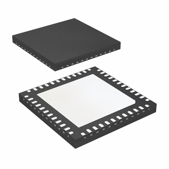
48-lead, 7.0mm x 7.0mm VFQFN
REVISION 2 05/18/15
1
©2015 Integrated Device Technology, Inc.
�840NT4-01 DATA SHEET
Block Diagram
VDD
OE_REF
VDDO_REF
Pullup
25MHz
QREF
OE_A
OE_B
Pullup
Pullup
VDDO_A
PLL_SELA
XTAL_SEL
Pullup
125MHz
Pulldown
QA0
XTAL_IN
VDDA
OSC
25MHz
QA1
Femtoclock®NG
XTAL_OUT
PCLK
nPCLK
Pulldown
QA2
Phase Detector
Pullup/
Pulldown
VCO
5
QA3
÷M
PDIV_SEL
Pulldown
QA4
÷N1
VDDO_B
125MHz/
25MHz
QB0
÷N2
QB1
QB2
PSELB
PLL_SELB
OE_C
Pulldown
Pullup
VDDO_C
Pullup
÷NFRAC
ETHERNET & USB CLOCK GENERATOR FOR FREESCALE
B4/T4-BASED SYSTEMS
2
24MHz
QC
REVISION 2 05/18/15
�840NT4-01 DATA SHEET
Pin Description and Pin Characteristic Tables
Table 2. Pin Descriptions1
Number
Name
Type
Description
1
XTAL_IN
Input
2
XTAL_OUT
Input
3
VDD_XTAL
Power
4
PCLK
Input
Pulldown
Non-inverting external 25MHz differential LVPECL reference input.
LVPECL input levels.
5
nPCLK
Input
Pullup/
Pulldown
Inverting external 25MHz differential LVPECL reference input.
LVPECL input levels.
6
GND
Power
Power supply ground.
7
VDD
Power
Core supply pins.
8
PDIV_SEL
Input
9
GND_DSM
Power
10
OE_REF
Input
11
VDDO_REF
Power
Output power supply for QREF output.
12
QREF
Output
Single-ended 25MHz, reference clock output. LVCMOS/LVTTL interface levels.
13
GND_REF
Power
Ground pin for QREF clock output.
14
OE_C
Input
15
GND_QC
Power
Ground pin for QC clock output.
16
QC
Output
Single-ended 24MHz, USB clock output. LVCMOS/LVTTL interface levels.
17
VDDO_C
Power
Output power supply for QC output.
18
OE_B
Input
19
VDDO_B
Power
20
QB2
Output
21
QB1
Output
22
QB0
Output
23
VDDO_B
Power
Output power supply for Bank QBx clock outputs.
24
GND_QB
Power
Ground pin for Bank QBx clock outputs.
25
GND
Power
Power supply ground.
26
GND_QA
Power
Ground pin for Bank QAx clock outputs.
27
QA4
Output
28
QA3
Output
29
QA2
Output
30
VDDO_A
Power
31
VDDO_A
Power
Crystal oscillator interface. XTAL_IN is the input, XTAL_OUT is the output.
REVISION 2 05/18/15
Power supply pin for XTAL.
Pulldown
Selects input for PCLK (LOW) or 5 pre-divider (HIGH).
LVCMOS/LVTTL interface levels.
Ground pin for Delta Sigma Modulator.
Pullup
Pullup
Pullup
Output enable for QREF output. The output is placed in a high-impedance mode
on disable. LVCMOS/LVTTL interface levels.
Output enable for QC output. The QC output is placed in a high-impedance
mode on disable. LVCMOS/LVTTL interface levels.
Output enable for Bank QBx outputs. The output bank is placed in a
high-impedance mode on disable. LVCMOS/LVTTL interface levels.
Output power supply for Bank QBx clock outputs.
Single-ended 125MHz or 25MHz clock outputs.
LVCMOS/LVTTL interface levels.
Single-ended output clocks, optimized at 125MHz.
LVCMOS/LVTTL interface levels.
Output power supply for Bank QAx clock outputs.
3
ETHERNET & USB CLOCK GENERATOR FOR FREESCALE
B4/T4-BASED SYSTEMS
�840NT4-01 DATA SHEET
Table 2. Pin Descriptions1 (Continued)
Number
Name
Type
Description
32
QA1
Output
33
QA0
Output
34
OE_A
Input
35
GND_QA
Power
Ground pin for Bank QAx clock outputs.
36
GND
Power
Power supply ground.
37
VDD
Power
Core supply pins.
38
PSELB
Input
Pulldown
39
PLL_SELA
Input
Pullup
Bypasses the PLL for Bank A outputs. When LOW, selects PLL (PLL Enable).
When HIGH, bypasses the PLL. LVCMOS/LVTTL interface levels.
40
PLL_SELB
Input
Pullup
Select pin for Bank B second stage mux. Designed to operate with a phase
detector input frequency of 25MHz. The Bank B outputs generate 125MHz when
select pin is LOW and 25MHz when HIGH. LVCMOS/LVTTL interface levels.
41
GNDA
Power
Ground pin for PLL analog.
42
VDDA
Power
Analog supply pin.
43
GND
Power
Power supply ground.
44
VDD
Power
Core supply pins.
45
RESERVED
Reserved
46
VDD
Power
47
XTAL_SEL
Input
48
GND_XTAL
Power
Single-ended output clocks, optimized at 125MHz.
LVCMOS/LVTTL interface levels.
Pullup
Output enable for Bank QAx outputs. The output bank is placed in a
high-impedance mode on disable. LVCMOS/LVTTL interface levels.
Select pin for Bank QBx first stage mux. Selects input for PLL enabled 25MHz
(LOW) or phase detector input frequency (HIGH). LVCMOS/LVTTL interface levels.
Reserved pin. Do not connect.
Core supply pins.
Pulldown
Select input for XTAL (LOW) or PCLK pre-divider (HIGH).
LVCMOS/LVTTL interface levels.
Ground pin for XTAL.
NOTE 1: Pullup and Pulldown refer to internal input resistors. See Table 2, Pin Characteristics, for typical values.
Table 3. Pin Characteristics1
Symbol
Parameter
CIN
PDIV_SEL, OE_REF, OE_A,
Input
OE_B, OE_C, PLL_SELA,
Capacitance
PLL_SELB, PSELB, XTAL_SEL
CPD
Power Dissipation
Capacitance (per output)
Test Conditions
Minimum
Typical
Maximum
Units
3.5
pF
VDDO_X = 3.465V
9
pF
VDDO_X = 2.625V
8
pF
VDDO_X = 1.89V
5
pF
RPULLUP
Input Pullup Resistor
50
k
RPULLDOWN
Input Pulldown Resistor
50
k
VDDO_X = 3.3V
15
VDDO_X = 2.5V
18
VDDO_X = 1.8V
26
ROUT
Output Impedance
NOTE 1: VDDO_X denotes, VDDO_A, VDDO_B, VDDO_C, VDDO_REF.
ETHERNET & USB CLOCK GENERATOR FOR FREESCALE
B4/T4-BASED SYSTEMS
4
REVISION 2 05/18/15
�840NT4-01 DATA SHEET
Absolute Maximum Ratings
NOTE: Stresses beyond those listed under Absolute Maximum Ratings may cause permanent damage to the device. These ratings are stress
specifications only. Functional operation of product at these conditions or any conditions beyond those listed in the DC Electrical Characteristics
or AC Electrical Characteristicsis not implied. Exposure to absolute maximum rating conditions for extended periods may affect product reliability.
Item
Rating
Supply Voltage, VDD
3.63V
Inputs, VI
XTAL_IN
0V to 2V
Other Inputs
-0.5V to VDD + 0.5V
Outputs, VO
-0.5V to VDDO_X + 0.5V
Junction Temperature
125C
Storage Temperature, TSTG
-65C to 150C
NOTE: VDDO_X denotes VDDO_A, VDDO_B, VDDO_C & VDDO_REF.
DC Electrical Characteristics
Table 4A. Power Supply DC Characteristics, VDD = VDD_XTAL = VDDO_X = 3.3V ± 5%, TA = -40°C to 85°C1, 2
Symbol
Parameter
VDD
Test Conditions
Minimum
Typical
Maximum
Units
Core Supply Voltage
3.135
3.3
3.465
V
VDD_XTAL
XTAL Power Supply Voltage
3.135
3.3
3.465
V
VDDA
Analog Supply Voltage
VDD – 0.06
3.3
VDD
V
VDDO_X
Output Supply Voltage
3.135
3.3
3.465
V
IDD +
IDD_XTAL
Power Supply Current
150
mA
IDDA
Analog Supply Current
30
mA
IDDO_X
Output Supply Current
8
mA
Outputs are Disabled to
High-Impedance
NOTE 1: VDDO_X denotes, VDDO_A, VDDO_B, VDDO_C, VDDO_REF.
NOTE 2: IDDO_X denotes, IDDO_A + IDDO_B + IDDO_C + IDDO_REF.
Table 4B. Power Supply DC Characteristics, VDD = VDD_XTAL = 3.3V ± 5%, VDDO_X = 2.5V ± 5%, TA = -40°C to 85°C1, 2
Symbol
Parameter
VDD
Test Conditions
Minimum
Typical
Maximum
Units
Core Supply Voltage
3.135
3.3
3.465
V
VDD_XTAL
XTAL Power Supply Voltage
3.135
3.3
3.465
V
VDDA
Analog Supply Voltage
VDD – 0.06
3.3
VDD
V
VDDO_X
Output Supply Voltage
2.375
2.5
2.625
V
IDD +
IDD_XTAL
Power Supply Current
150
mA
IDDA
Analog Supply Current
30
mA
IDDO_X
Output Supply Current
4
mA
Outputs are Disabled to
High-Impedance
NOTE 1: VDDO_X denotes, VDDO_A, VDDO_B, VDDO_C, VDDO_REF.
NOTE 2: IDDO_X denotes, IDDO_A + IDDO_B + IDDO_C + IDDO_REF.
REVISION 2 05/18/15
5
ETHERNET & USB CLOCK GENERATOR FOR FREESCALE
B4/T4-BASED SYSTEMS
�840NT4-01 DATA SHEET
Table 4C. Power Supply DC Characteristics, VDD = VDD_XTAL = 3.3V ± 5%, VDDO_x = 1.8V ± 5%, TA = -40°C to 85°C1, 2
Symbol
Parameter
VDD
Test Conditions
Minimum
Typical
Maximum
Units
Core Supply Voltage
3.135
3.3
3.465
V
VDD_XTAL
XTAL Power Supply Voltage
3.135
3.3
3.465
V
VDDA
Analog Supply Voltage
VDD – 0.06
3.3
VDD
V
VDDO_X
Output Supply Voltage
1.71
1.8
1.89
V
IDD +
IDD_XTAL
Power Supply Current
150
mA
IDDA
Analog Supply Current
30
mA
IDDO_X
Output Supply Current
3
mA
Outputs are Disabled to
High-Impedance
NOTE 1: VDDO_X denotes, VDDO_A, VDDO_B, VDDO_C, VDDO_REF.
NOTE 2: IDDO_X denotes, IDDO_A + IDDO_B + IDDO_C + IDDO_REF.
Table 4D. Power Supply DC Characteristics, VDD = VDD_XTAL = VDDO_X = 2.5V ± 5%, TA = -40°C to 85°C1, 2
Symbol
Parameter
VDD
Test Conditions
Minimum
Typical
Maximum
Units
Core Supply Voltage
2.375
2.5
2.625
V
VDD_XTAL
XTAL Power Supply Voltage
2.375
2.5
2.625
V
VDDA
Analog Supply Voltage
VDD – 0.054
2.5
VDD
V
VDDO_X
Output Supply Voltage
2.375
2.5
2.625
V
IDD +
IDD_XTAL
Power Supply Current
148
mA
IDDA
Analog Supply Current
27
mA
IDDO_X
Output Supply Current
4
mA
Outputs are Disabled to
High-Impedance
NOTE 1: VDDO_X denotes, VDDO_A, VDDO_B, VDDO_C, VDDO_REF.
NOTE 2: IDDO_X denotes, IDDO_A + IDDO_B + IDDO_C + IDDO_REF.
Table 4E. Power Supply DC Characteristics, VDD = VDD_XTAL = 2.5V ± 5%, VDDO_X = 1.8V ± 5%, TA = -40°C to 85°C1, 2
Symbol
Parameter
VDD
Test Conditions
Minimum
Typical
Maximum
Units
Core Supply Voltage
2.375
2.5
2.625
V
VDD_XTAL
XTAL Power Supply Voltage
2.375
2.5
2.625
V
VDDA
Analog Supply Voltage
VDD – 0.054
2.5
VDD
V
VDDO_X
Output Supply Voltage
1.71
1.8
1.89
V
IDD +
IDD_XTAL
Power Supply Current
148
mA
IDDA
Analog Supply Current
27
mA
IDDO_X
Output Supply Current
3
mA
Outputs are Disabled to
High-Impedance
NOTE 1: VDDO_X denotes, VDDO_A, VDDO_B, VDDO_C, VDDO_REF.
NOTE 2: IDDO_X denotes, IDDO_A + IDDO_B + IDDO_C + IDDO_REF.
ETHERNET & USB CLOCK GENERATOR FOR FREESCALE
B4/T4-BASED SYSTEMS
6
REVISION 2 05/18/15
�840NT4-01 DATA SHEET
Table 4F. LVCMOS/LVTTL DC Characteristics, TA = -40°C to 85°C1
Symbol
Parameter
VIH
Input High Voltage
VIL
Input Low Voltage
IIH
IIL
VOH
VOL
Input
High Current
Input
Low Current
Test Conditions
Minimum
VDD = 3.3V ± 5%
Typical
Maximum
Units
2
VDD + 0.3
V
VDD = 2.5V ± 5%
1.7
VDD + 0.3
V
VDD = 3.3V ± 5%
-0.3
0.8
V
VDD = 2.5V ± 5%
-0.3
0.7
V
PSELB, XTAL_SEL,
PDIV_SEL
VDD = VIN = 3.465V or 2.625V
150
µA
OE_REF, PLL_SELA,
PLL_SELB, OE_A,
OE_B, OE_C
VDD = VIN = 3.465V or 2.625V
5
µA
PSELB, XTAL_SEL,
PDIV_SEL
VDD = 3.465V or 2.625V,
VIN = 0V
-5
µA
OE_REF, PLL_SELA,
PLL_SELB, OE_A,
OE_B, OE_C
VDD = 3.465V or 2.625V,
VIN = 0V
-150
µA
VDDO_X = 3.3V ± 5%; IOH = -12mA
2.6
V
VDDO_X = 2.5V ± 5%; IOH = -12mA
1.8
V
VDDO_X = 1.8V ± 5%; IOH = -8mA
1.3
V
Output High Voltage
Output Low Voltage;
VDDO_X= 3.3V ± 5%, IOL = 12mA
0.5
V
VDDO_X= 2.5V ± 5%, IOL = 12mA
0.5
V
VDDO_X = 1.8V ± 5%, IOL = 8mA
0.4
V
Maximum
Units
150
µA
NOTE 1: VDDO_X denotes, VDDO_A, VDDO_B, VDDO_C, VDDO_REF.
Table 4G. LVPECL Differential DC Characteristics, VDD = 3.3V ± 5% or 2.5V ± 5%, TA = -40°C to 85°C
Symbol
Parameter
IIH
Input High
Current
IIL
Input Low
Current
Test Conditions
PCLK, nPCLK
Minimum
VDD = VIN = 3.465V or 2.625V
Typical
PCLK
VDD = 3.465V or 2.625V,
VIN = 0V
-5
µA
nPCLK
VDD = 3.465V or 2.625V,
VIN = 0V
-150
µA
VPP
Peak-to-Peak Voltage1
VCMR
Common Mode Input Voltage1, 2
0.3
1.0
V
GND + 1.5
VDD
V
NOTE 1: VIL should not be less than -0.3V and VIH should not be greater than VDD..
NOTE 2: Common mode voltage is defined at the crosspoint.
REVISION 2 05/18/15
7
ETHERNET & USB CLOCK GENERATOR FOR FREESCALE
B4/T4-BASED SYSTEMS
�840NT4-01 DATA SHEET
Table 5. Input Frequency Characteristics, VDD = VDD_XTAL = 3.3V ± 5% or 2.5V ± 5%, TA = -40°C to 85°C
Symbol
Parameter
Test Conditions
Minimum
Typical
XTAL_IN, XTAL_OUT
fIN
Input
Frequency
Maximum
Units
25
MHz
PDIV_SEL = 0
25
MHz
PDIV_SEL = 1
125
MHz
PCLK, nPCLK
Table 6. Crystal Characteristics1
Parameter
Test Conditions
Mode of Oscillation
Minimum
Typical
Maximum
Units
Fundamental
Frequency
25
Load Capacitance (CL)
12
MHz
18
pF
Equivalent Series Resistance (ESR)
50
Shunt Capacitance
7
pF
NOTE 1: IDT Part#603-25-173 recommended.
ETHERNET & USB CLOCK GENERATOR FOR FREESCALE
B4/T4-BASED SYSTEMS
8
REVISION 2 05/18/15
�840NT4-01 DATA SHEET
AC Electrical Characteristics
Table 7. AC Characteristics, VDD = VDD_XTAL = 3.3V ± 5% or 2.5V ± 5%, VDDO_A, VDDO_B, VDDO_C, VDDO_REF = 3.3V ± 5%
or 2.5V ± 5% or 1.8V ± 5%, TA = -40°C to 85°C1
Symbol
Parameter
fOUT
Output Frequency
2, 3
Test Conditions
Minimum
PLL Mode
24
Typical
Maximum
Units
125
MHz
tsk(o)
Output Skew
fOUT = 125MHz
120
ps
tsk(b)
Bank Skew2, 4
fOUT = 125MHz
50
ps
QA[0:4]
0.60
ps
QB[0:2]
1.20
ps
QA[0:4]
0.45
ps
QB[0:2]
0.93
ps
QA[0:4]
0.40
ps
QB[0:2]
0.76
ps
VDDO = 3.3V
tjit(Ø)
Phase Jitter, RMS;
Integration Range:
12kHz – 20MHz5, 6
VDDO = 2.5V
VDDO = 1.8V
Jitter2, 5
tjit(cc)
Cycle-to-Cycle
tjit(per)
RMS Period Jitter2, 5
tL
PLL Lock Time
odc
Output Duty Cycle
tR / tF
Output Rise/Fall Time
fOUT = 125MHz
20
45
ps
fOUT = 125MHz
3
6
ps
13
PLL Mode (QAx, QBx, QC)
20% to 80%
45
ms
55
%
900
ps
NOTE 1: Electrical parameters are guaranteed over the specified ambient operating temperature range, which is established when the device
is mounted in a test socket with maintained transverse airflow greater than 500 lfpm. The device will meet specifications after thermal
equilibrium has been reached under these conditions.
NOTE 2: This parameter is defined in accordance with JEDEC Standard 65.
NOTE 3: Defined as skew between outputs at the same supply voltage and with equal load conditions.
NOTE 4: Defined as skew within a bank of outputs at the same voltage and with equal load conditions.
NOTE 5: Jitter performance using XTAL inputs.
NOTE 6: Measured with Bank A at 125MHz, Bank B at 125MHz, QC and QREF enabled.
REVISION 2 05/18/15
9
ETHERNET & USB CLOCK GENERATOR FOR FREESCALE
B4/T4-BASED SYSTEMS
�840NT4-01 DATA SHEET
Noise Power (dBc/Hz)
Typical Phase Noise at 125MHz
Offset Frequency (Hz)
ETHERNET & USB CLOCK GENERATOR FOR FREESCALE
B4/T4-BASED SYSTEMS
10
REVISION 2 05/18/15
�840NT4-01 DATA SHEET
Parameter Measurement Information
1.25V±5%
1.65V±5%
1.65V±5%
1.25V±5%
SCOPE
VDD,
VDD_XTAL,
VDDO_X
VDDA
VDD,
VDD_XTAL,
VDDO_X
Q
GND
SCOPE
VDDA
Q
GND
-1.25V±5%
-1.65V±5%
2.5V Core/2.5V LVCMOS Output Load Test Circuit
3.3V Core/3.3V LVCMOS Output Load Test Circuit
2.05V±5%
2.4V±5%
1.25V±5%
0.9V±5%
2.05V±5%
2.4V±5%
VDD,
VDD_XTAL
SCOPE
VDD,
VDD_XTAL
SCOPE
VDDO_X
VDDO_X
VDDA
Qx
VDDA
GND
Qx
GND
-0.9V±5%
-1.25V±5%
3.3V Core/1.8V LVCMOS Output Load Test Circuit
3.3V Core/2.5V LVCMOS Output Load Test Circuit
1.6V±5%
0.9V±5%
VDD
1.6V±5%
SCOPE
VDD,
VDD_XTAL
VDDO_X
VDDA
PCLK
Qx
nPCLK
GND
GND
-0.9V±5%
Differential Input Level
2.5V Core/1.8V LVCMOS Output Load Test Circuit
REVISION 2 05/18/15
11
ETHERNET & USB CLOCK GENERATOR FOR FREESCALE
B4/T4-BASED SYSTEMS
�840NT4-01 DATA SHEET
Parameter Measurement Information, continued
PLL Lock Time
RMS Phase Jitter
VOH
VREF
V
1σ contains 68.26% of all measurements
2σ contains 95.4% of all measurements
3σ contains 99.73% of all measurements
4σ contains 99.99366% of all measurements
6σ contains (100-1.973x10⁻⁷)% of all measurements
V
DDO_X
2
DDO_X
2
➤
tcycle n
➤
VOL
V
DDO_X
QAx,
QBx
➤
2
tcycle n+1
➤
tjit(cc) = |tcycle n – tcycle n+1|
1000 Cycles
Histogram
Reference Point
Mean Period
(Trigger Edge)
(First edge after trigger)
RMS Period Jitter
QXx
Cycle-to-Cycle Jitter
V
VDDO_X
2
DDOX
QXx
VDDO_X
2
QXy
2
V
DDOX
QXy
2
tsk(o)
tsk(b)
Bank Skew
Output Skew
V
DDO_X
QAx,
QBx, QC
2
t PW
80%
t
odc =
80%
PERIOD
t PW
QAx,
QBx, QC
20%
20%
x 100%
tR
tF
t PERIOD
Output Rise Fall Time
Output Duty Cycle/Pulse Width/Period
ETHERNET & USB CLOCK GENERATOR FOR FREESCALE
B4/T4-BASED SYSTEMS
12
REVISION 2 05/18/15
�840NT4-01 DATA SHEET
Applications Information
Recommendations for Unused Input and Output Pins
Inputs:
Outputs:
LVCMOS Control Pins
LVCMOS Outputs
All control pins have internal pullups or pulldowns; additional
resistance is not required but can be added for additional protection.
A 1k resistor can be used.
All unused LVCMOS outputs can be left floating. There should be no
trace attached.
PCLK/nPCLK Inputs
For applications not requiring the use of the differential input, both
PCLK and nPCLK can be left floating. Though not required, but for
additional protection, a 1k resistor can be tied from PCLK to
ground.
Crystal Inputs
For applications not requiring the use of the crystal oscillator input,
both XTAL_IN and XTAL_OUT can be left floating. Though not
required, but for additional protection, a 1k resistor can be tied from
XTAL_IN to ground.
REVISION 2 05/18/15
13
ETHERNET & USB CLOCK GENERATOR FOR FREESCALE
B4/T4-BASED SYSTEMS
�840NT4-01 DATA SHEET
Overdriving the XTAL Interface
The XTAL_IN input can be overdriven by an LVCMOS driver or by one
side of a differential driver through an AC coupling capacitor. The
XTAL_OUT pin can be left floating. The amplitude of the input signal
should be between 500mV and 1.8V and the slew rate should not be
less than 0.2V/nS. For 3.3V LVCMOS inputs, the amplitude must be
reduced from full swing to at least half the swing in order to prevent
signal interference with the power rail and to reduce internal noise.
Figure 1A shows an example of the interface diagram for a high
speed 3.3V LVCMOS driver. This configuration requires that the sum
of the output impedance of the driver (Ro) and the series resistance
(Rs) equals the transmission line impedance. In addition, matched
termination at the crystal input will attenuate the signal in half. This
VDD
can be done in one of two ways. First, R1 and R2 in parallel should
equal the transmission line impedance. For most 50 applications,
R1 and R2 can be 100. This can also be accomplished by removing
R1 and changing R2 to 50. The values of the resistors can be
increased to reduce the loading for a slower and weaker LVCMOS
driver. Figure 1B shows an example of the interface diagram for an
LVPECL driver. This is a standard LVPECL termination with one side
of the driver feeding the XTAL_IN input. It is recommended that all
components in the schematics be placed in the layout. Though some
components might not be used, they can be utilized for debugging
purposes. The datasheet specifications are characterized and
guaranteed by using a quartz crystal as the input.
XTAL_OUT
R1
100
Ro
Zo = 50 ohms
C1
Rs
XTAL_IN
R2
100
Zo = Ro + Rs
.1uf
LVCMOS Driver
Figure 1A. General Diagram for LVCMOS Driver to XTAL Input Interface
XTAL_OUT
C2
Zo = 50 ohms
XTAL_IN
.1uf
Zo = 50 ohms
LVPECL Driver
R1
50
R2
50
R3
50
Figure 1B. General Diagram for LVPECL Driver to XTAL Input Interface
ETHERNET & USB CLOCK GENERATOR FOR FREESCALE
B4/T4-BASED SYSTEMS
14
REVISION 2 05/18/15
�840NT4-01 DATA SHEET
3.3V LVPECL Clock Input Interface
input interfaces suggested here are examples only. If the driver is
from another vendor, use their termination recommendation. Please
consult with the vendor of the driver component to confirm the driver
termination requirements.
The PCLK /nPCLK accepts LVPECL and other differential signals.
Both VSWING and VOH must meet the VPP and VCMR input
requirements. Figure 2A to Figure 2B show interface examples for the
PCLK/nPCLK input driven by the most common driver types. The
3.3V
3.3V
3.3V
R3
125Ω
R4
125Ω
Zo = 50Ω
PCLK
Zo = 50Ω
nPCLK
LVPECL
Input
LVPECL
R1
84Ω
Figure 2A. PCLK/nPCLK Input Driven by a
3.3V LVPECL Driver with AC Couple
R2
84Ω
Figure 2B. PCLK/nPCLK Input Driven by a
3.3V LVPECL Driver
2.5V LVPECL Clock Input Interface
input interfaces suggested here are examples only. If the driver is
from another vendor, use their termination recommendation. Please
consult with the vendor of the driver component to confirm the driver
termination requirements.
The PCLK /nPCLK accepts LVPECL and other differential signals.
Both VSWING and VOH must meet the VPP and VCMR input
requirements. Figure 3A to Figure 3B show interface examples for the
PCLK/nPCLK input driven by the most common driver types. The
2.5V
2.5V
2.5V
PCLK
nPCLK
LVPECL
Figure 3A. PCLK/nPCLK Input Driven by a
3.3V LVPECL Driver with AC Couple
REVISION 2 05/18/15
LVPECL
Input
Figure 3B. PCLK/nPCLK Input Driven by a
3.3V LVPECL Driver
15
ETHERNET & USB CLOCK GENERATOR FOR FREESCALE
B4/T4-BASED SYSTEMS
�840NT4-01 DATA SHEET
VFQFN EPAD Thermal Release Path
In order to maximize both the removal of heat from the package and
the electrical performance, a land pattern must be incorporated on
the Printed Circuit Board (PCB) within the footprint of the package
corresponding to the exposed metal pad or exposed heat slug on the
package, as shown in Figure 4. The solderable area on the PCB, as
defined by the solder mask, should be at least the same size/shape
as the exposed pad/slug area on the package to maximize the
thermal/electrical performance. Sufficient clearance should be
designed on the PCB between the outer edges of the land pattern
and the inner edges of pad pattern for the leads to avoid any shorts.
and dependent upon the package power dissipation as well as
electrical conductivity requirements. Thus, thermal and electrical
analysis and/or testing are recommended to determine the minimum
number needed. Maximum thermal and electrical performance is
achieved when an array of vias is incorporated in the land pattern. It
is recommended to use as many vias connected to ground as
possible. It is also recommended that the via diameter should be 12
to 13mils (0.30 to 0.33mm) with 1oz copper via barrel plating. This is
desirable to avoid any solder wicking inside the via during the
soldering process which may result in voids in solder between the
exposed pad/slug and the thermal land. Precautions should be taken
to eliminate any solder voids between the exposed heat slug and the
land pattern. Note: These recommendations are to be used as a
guideline only. For further information, please refer to the Application
Note on the Surface Mount Assembly of Amkor’s Thermally/
Electrically Enhance Leadframe Base Package, Amkor Technology.
While the land pattern on the PCB provides a means of heat transfer
and electrical grounding from the package to the board through a
solder joint, thermal vias are necessary to effectively conduct from
the surface of the PCB to the ground plane(s). The land pattern must
be connected to ground through these vias. The vias act as “heat
pipes”. The number of vias (i.e. “heat pipes”) are application specific
PIN
PIN PAD
SOLDER
EXPOSED HEAT SLUG
GROUND PLANE
THERMAL VIA
SOLDER
PIN
LAND PATTERN
(GROUND PAD)
PIN PAD
Figure 4. P.C. Assembly for Exposed Pad Thermal Release Path – Side View (drawing not to scale)
ETHERNET & USB CLOCK GENERATOR FOR FREESCALE
B4/T4-BASED SYSTEMS
16
REVISION 2 05/18/15
�840NT4-01 DATA SHEET
Schematic Example
Figure 5 (next page) shows an example 840NT4-01 application
schematic. This schematic example focuses on functional
connections and is not configuration specific. Refer to the pin
description and functional tables in the datasheet to ensure that the
logic control inputs are properly set. In this schematic, the device is
operated at VDD = VDDA = 2.5V and VDDO_A, VDDO_B, VDDO_C and
VDDO_REF = 1.8V.
ground plane and all deeper layers until the next ground plane is
reached. The ground connection of the tuning capacitors should first
be made between the capacitors on the top layer, then a single
ground via is dropped to connect the tuning cap ground to the ground
plane as close to the 840NT4-01 as possible as shown in the
schematic.
This device package has an ePAD that is connected to ground
internally. The ePAD is to be connected to VEE/GND through vias in
order to improve heat dissipation.
A 12pF parallel resonant 25MHz crystal (IDT/ Fox Part #603-25-173)
is used with the recommended load capacitors C1 = C2 = 3.3pF for
frequency accuracy. Depending on the parasitic capacity on the
crystal terminals of the printed circuit board layout, these values
might require a slight adjustment to optimize the frequency accuracy.
Crystals with other load capacitance specifications can be used. This
will require adjusting C1 and C2. For this device, the crystal load
capacitors are required for proper operation.
As with any high speed analog circuitry, the power supply pins are
vulnerable to random noise. To achieve optimum jitter performance,
power supply isolation is required. The 840NT4-01 provides separate
power supply pins to isolate any high switching noise from coupling
into the internal PLL.
Crystal layout is very important to minimize capacitive coupling
between the crystal pads and leads and other metal in the circuit
board. Capacitive coupling to other conductors has two adverse
effects; it reduces the oscillator frequency leaving less tuning margin
and noise coupling from power planes and logic transitions on signal
traces can pull the phase of the crystal resonance, inducing jitter.
Routing I2C under the crystal is a very common layout error, based
on the assumption that it is a low frequency signal and will not affect
the crystal oscillation. In fact, I2C transition times are short enough to
capacitively couple into the crystal if they are routed close enough to
the crystal traces.
In order to achieve the best possible filtering, it is recommended that
the placement of the filter components be on the device side of the
PCB as close to the power pins as possible. If space is limited, the
0.1F capacitor in each power pin filter should be placed on the
device side. The other components can be on the opposite side of the
PCB.
Power supply filter recommendations are a general guideline to be
used for reducing external noise from coupling into the devices. The
filter performance is designed for a wide range of noise frequencies.
This low-pass filter starts to attenuate noise at approximately 10kHz.
If a specific frequency noise component is known, such as switching
power supplies frequencies, it is recommended that component
values be adjusted and if required, additional filtering be added.
Additionally, good general design practices for power plane voltage
stability suggests adding bulk capacitance in the local area of all
devices.
In layout, all capacitive coupling to the crystal from any signal trace is
to be minimized, that is to the XTAL_IN and XTAL_OUT pins, traces
to the crystal pads, the crystal pads and the tuning capacitors. Using
a crystal on the top layer as an example, void all signal and power
layers under the crystal connections between the top layer and the
ground plane used by the 840NT4-01. Then calculate the parasitic
capacity to the ground and determine if it is large enough to preclude
tuning the oscillator. If the coupling is excessive, particularly if the first
layer under the crystal is a ground plane, a layout option is to void the
REVISION 2 05/18/15
For additional layout recommendations and guidelines, contact
clocks@idt.com.
17
ETHERNET & USB CLOCK GENERATOR FOR FREESCALE
B4/T4-BASED SYSTEMS
�840NT4-01 DATA SHEET
Logic Contr ol Input Examples
V DD
Set Logic
Input to ' 1'
VD D
RU1
1k
2. 5V
To Logic
Input
pins
RD1
N ot Ins t all
1
B LM18BB 221S N 1
RU2
N ot I ns tall
To Logic
Input
pins
FB 1
2
V DD
Set Logic
Input to '0'
R5
C4
10uF
2
C3
0. 1uF
V D DA
C6
0. 1uF
C 11
0.1uF
C 16
0. 1uF
C 17
0.1uF
C 18
0. 1uF
C5
10uF
VD D
RD2
1k
1. 8V
F B2
V D DO
2
1
46
44
42
V D DA
VD D A
OE_R EF
OE_A
OE_B
OE_C
10
34
18
14
PLL_S ELA
PSE LB
PLL_S ELB
39
38
40
XTA L_S EL
PD I V_SE L
47
8
45
C7
0.1uF
OE_R EF
OE_A
OE_B
OE_C
GN D A
PLL_SELA
PS ELB
PLL_SELB
VD D O_R E F
R ES ER VE D
IDT/ FOX
603-25-173 crystal
Fox 325BS crystal
4
1
X1
3
2
GN D _QA
GN D _QA
C 14
0.1uF
30
31
V DDO
C 15
0.1uF
26
35
XTA L_OU T
25 MHz
(12pF)
XTA L_I N
VD D O
11
GN D _R E F
VD D O_A
VD D O_A
XTA L_OU T
VD D O_B
VD D O_B
19
23
V DDO
1
C 10
0.1uF
XTA L_I N
2
24
C1
3.3pF
C2
3.3pF
Place each 0.1uF
bypass cap directly
adjacent to the
corresponding VDD,
VDDA or VDDO_x pin.
41
13
XTA L_S EL
PD I V_SE L
C8
0. 1uF
VD D
VD D
V DD
37
7
V DD
U1
V DD
3
BLM18B B221SN 1
C9
10uF
C 12
0. 1uF
GN D _QB
48
GN D _XTAL
17
VD D O
V D DO_C
C 13
0.1uF
GN D_QC
15
Zo = 50 Ohm
R2
R1
50
4
5
Zo = 50 Ohm
R6
QR E F
12
QRE F
PC LK
Zo = 50
24
nPC LK
50
QA0
QA1
QA2
QA3
QA4
2. 5V PE C L D riv er
R7
25
QB0
QB1
QB2
33
32
29
28
27
QA0
QA1
QA2
QA3
QA4
22
21
20
QB0
QB1
QB2
16
QC
1. 8V LVC MOS R eceiv er
R3
Zo = 50
eP AD
1. 8V LVC MOS R eceiv er
49
GN D
GN D
43
GN D
36
6
GN D
24
25
9
GN D _D SM
QC
Figure 5. 840NT4-01 Schematic Layout
ETHERNET & USB CLOCK GENERATOR FOR FREESCALE
B4/T4-BASED SYSTEMS
18
REVISION 2 05/18/15
�840NT4-01 DATA SHEET
Power Considerations
This section provides information on power dissipation and junction temperature for the 840NT4-01.
Equations and example calculations are also provided.
1.
Power Dissipation.
The total power dissipation for the 840NT4-01 is the sum of the static power plus the dynamic power dissipation due to loading. The following
is the power dissipation for VDD = 3.3V +5% = 3.465V, which gives worst case results.
The maximum core current at 85°C, IDDmax = 150mA
Static Power (max)
= [VDD_MAX * (IDD_MAX + IDD_XTAL + IDDA + IDDO_X)]
= [3.465V * (150mA + 30mA + 8mA)]
= 651.4mW
Dynamic Power Dissipation (max), Clocks for Freescale B4/T4 Processor
= [CPD * (N * Frequency + N * Frequency + N * Frequency) * (VDDO)2]
= [9pF *(8 * 125MHz + 1 * 25MHz + 1 * 24MHz) * (3.465V)2]
= 113.4mW
Total Power
= Static Power + Dynamic Power Dissipation
= 651.4mW + 113.4mW
= 0.765W
2. Junction Temperature.
Junction temperature, Tj, is the temperature at the junction of the bond wire and bond pad, and directly affects the reliability of the device. The
maximum recommended junction temperature is 125°C. Limiting the internal transistor junction temperature, Tj, to 125°C ensures that the bond
wire and bond pad temperature remains below 125°C.
The equation for Tj is as follows: Tj = JA * Pd_total + TA
Tj = Junction Temperature
JA = Junction-to-Ambient Thermal Resistance
Pd_total = Total Device Power Dissipation (example calculation is in section 1 above)
TA = Ambient Temperature
In order to calculate junction temperature, the appropriate junction-to-ambient thermal resistance JA must be used. Assuming no air flow and
a multi-layer board, the appropriate value is 30°C/W per Table 8 below.
Therefore, Tj for an ambient temperature of 85°C with all outputs switching is:
85°C + 0.765W * 30°C/W = 108°C. This is below the limit of 125°C.
This calculation is only an example. Tj will obviously vary depending on the number of loaded outputs, supply voltage, air flow and the type of
board (multi-layer).
Table 8. Thermal Resistance JA for a 48-lead VFQFN Package
JA by Velocity
Meters per Second
Multi-Layer PCB, JEDEC Standard Test Boards
REVISION 2 05/18/15
0
1
2
30°C/W
23.1°C/W
19.8°C/W
19
ETHERNET & USB CLOCK GENERATOR FOR FREESCALE
B4/T4-BASED SYSTEMS
�840NT4-01 DATA SHEET
Reliability Information
Table 9. JA vs. Air Flow Table for a 48-Lead VFQFN
JA by Velocity
Meters per Second
Multi-Layer PCB, JEDEC Standard Test Boards
0
1
2
30°C/W
23.1°C/W
19.8°C/W
Transistor Count
The transistor count for 840NT4-01 is: 24,508
ETHERNET & USB CLOCK GENERATOR FOR FREESCALE
B4/T4-BASED SYSTEMS
20
REVISION 2 05/18/15
�840NT4-01 DATA SHEET
48-Lead VFQFN Package Outline and Package Dimensions
REVISION 2 05/18/15
21
ETHERNET & USB CLOCK GENERATOR FOR FREESCALE
B4/T4-BASED SYSTEMS
�840NT4-01 DATA SHEET
Ordering Information
Table 10. Ordering Information
Part/Order Number
Marking
Package
Shipping Packaging
Temperature
840NT4-01NLGI
IDT840NT4-01NLGI
48-Lead VFQFN, Lead-Free
Tray
-40C to 85C
840NT4-01NLGI8
IDT840NT4-01NLGI
48-Lead VFQFN, Lead-Free
Tape & Reel
-40C to 85C
ETHERNET & USB CLOCK GENERATOR FOR FREESCALE
B4/T4-BASED SYSTEMS
22
REVISION 2 05/18/15
�840NT4-01 DATA SHEET
Revision History Sheet
Rev
Table
2
REVISION 2 05/18/15
Page
8
17
18
Description of Change
Date
Crystal Characteristics - added note.
Schematic Example - revised first sentence of paragraph 2.
840NT4-01 Schematic Layout - revised crystal note.
23
5/18/15
ETHERNET & USB CLOCK GENERATOR FOR FREESCALE
B4/T4-BASED SYSTEMS
�Corporate Headquarters
Sales
Tech Support
6024 Silver Creek Valley Road
San Jose, CA 95138 USA
1-800-345-7015 or 408-284-8200
Fax: 408-284-2775
www.IDT.com
email: clocks@idt.com
DISCLAIMER Integrated Device Technology, Inc. (IDT) and its subsidiaries reserve the right to modify the products and/or specifications described herein at any time and at IDT’s sole discretion. All information in
this document, including descriptions of product features and performance, is subject to change without notice. Performance specifications and the operating parameters of the described products are determined
in the independent state and are not guaranteed to perform the same way when installed in customer products. The information contained herein is provided without representation or warranty of any kind, whether
express or implied, including, but not limited to, the suitability of IDT’s products for any particular purpose, an implied warranty of merchantability, or non-infringement of the intellectual property rights of others. This
document is presented only as a guide and does not convey any license under intellectual property rights of IDT or any third parties.
IDT’s products are not intended for use in applications involving extreme environmental conditions or in life support systems or similar devices where the failure or malfunction of an IDT product can be reasonably
expected to significantly affect the health or safety of users. Anyone using an IDT product in such a manner does so at their own risk, absent an express, written agreement by IDT.
Integrated Device Technology, IDT and the IDT logo are registered trademarks of IDT. Product specification subject to change without notice. Other trademarks and service marks used herein, including protected
names, logos and designs, are the property of IDT or their respective third party owners.
Copyright ©2015 Integrated Device Technology, Inc.. All rights reserved.
�IMPORTANT NOTICE AND DISCLAIMER
RENESAS ELECTRONICS CORPORATION AND ITS SUBSIDIARIES (“RENESAS”) PROVIDES TECHNICAL
SPECIFICATIONS AND RELIABILITY DATA (INCLUDING DATASHEETS), DESIGN RESOURCES (INCLUDING
REFERENCE DESIGNS), APPLICATION OR OTHER DESIGN ADVICE, WEB TOOLS, SAFETY INFORMATION, AND
OTHER RESOURCES “AS IS” AND WITH ALL FAULTS, AND DISCLAIMS ALL WARRANTIES, EXPRESS OR IMPLIED,
INCLUDING, WITHOUT LIMITATION, ANY IMPLIED WARRANTIES OF MERCHANTABILITY, FITNESS FOR A
PARTICULAR PURPOSE, OR NON-INFRINGEMENT OF THIRD PARTY INTELLECTUAL PROPERTY RIGHTS.
These resources are intended for developers skilled in the art designing with Renesas products. You are solely responsible
for (1) selecting the appropriate products for your application, (2) designing, validating, and testing your application, and (3)
ensuring your application meets applicable standards, and any other safety, security, or other requirements. These
resources are subject to change without notice. Renesas grants you permission to use these resources only for
development of an application that uses Renesas products. Other reproduction or use of these resources is strictly
prohibited. No license is granted to any other Renesas intellectual property or to any third party intellectual property.
Renesas disclaims responsibility for, and you will fully indemnify Renesas and its representatives against, any claims,
damages, costs, losses, or liabilities arising out of your use of these resources. Renesas' products are provided only subject
to Renesas' Terms and Conditions of Sale or other applicable terms agreed to in writing. No use of any Renesas resources
expands or otherwise alters any applicable warranties or warranty disclaimers for these products.
(Rev.1.0 Mar 2020)
Corporate Headquarters
Contact Information
TOYOSU FORESIA, 3-2-24 Toyosu,
Koto-ku, Tokyo 135-0061, Japan
www.renesas.com
For further information on a product, technology, the most
up-to-date version of a document, or your nearest sales
office, please visit:
www.renesas.com/contact/
Trademarks
Renesas and the Renesas logo are trademarks of Renesas
Electronics Corporation. All trademarks and registered
trademarks are the property of their respective owners.
© 2020 Renesas Electronics Corporation. All rights reserved.
�