FemtoClock® Crystal-to-0.7V Differential
HCSL Clock Generator
ICS841402I
DATA SHEET
General Description
Features
The ICS841402I is an optimized PCIe and sRIO clock generator.
The device uses a 25MHz parallel resonant crystal to generate
100MHz, 125MHz, 200MHz and 400MHz clock signals, replacing
solutions requiring multiple oscillator and fanout buffer solutions. The
device has excellent phase jitter suitable to clock components
requiring precise and low jitter PCIe, sRIO or both clock signals. The
device also supports a configurable spread-spectrum generation for
PCIe applications. Designed for telecom, networking and industrial
applications, the ICS841402I can also drive the high-speed sRIO
and PCIe SerDes clock inputs of communications processors,
DSPs, switches and bridges.
•
Two 0.7V differential HCSL outputs: configurable for PCIe
(100MHz or 200MHz) and sRIO (125MHz) clock signals
•
•
One LVCMOS/LVTTL reference clock output
•
Supports the following output frequencies: 100MHz, 125MHz,
200MHz or 400MHz
•
•
•
•
VCO frequency range: 950MHz - 1.25GHz
•
PCI Express (2.5 Gb/S), Gen 2 (5 Gb/s) and Gen 3 (8 Gb/s) jitter
compliant (REF_OUT disabled)
•
•
•
Full 3.3V operating supply
Selectable crystal oscillator interface, 25MHz, 18pF parallel
resonant crystal or LVCMOS/LVTTL single-ended reference clock
input
Configurable spread-spectrum generation for PCIe
PLL bypass and output enable
RMS phase jitter @ 200MHz, using a 25MHz crystal
(12kHz – 20MHz): 1.21ps (typical)
-40°C to 85°C ambient operating temperature
Available in lead-free (RoHS 6) packages
Block Diagram
OE_REFOUT
Pulldown
25MHz
REF_OUT
25MHz
Pulldown
÷
Q1
nQ1
Pin Assignment
GND
M=
÷40, ÷48
IREF
SSM
Pulldown
BYPASS
Pulldown
FSEL[1:0]
MR/nOE
Pullup:Pulldown
SSM
REF_SEL
Spread-Spectrum
1
IREF
Pulldown
nQ0
BYPASS
REF_IN
0
Q0
VDD
FemtoClock
PLL
XTAL_OUT
N=
÷
÷
÷
VDDA
1
0
REF_SEL
OSC
REF_IN
XTAL_IN
32 31 30 29 28 27 26 25
2
Pulldown
XTAL_IN
1
24
VDD
XTAL_OUT
2
23
FSEL1
MR/nOE
3
VDD
4
Q0
5
nQ0
6
Q1
7
nQ1
8
ICS841402I
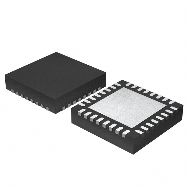
32-Lead VFQFN
5mm x 5mm x 0.925mm
package body
K Package
Top View
22
FSEL0
21
REF_OUT
20
OE_REFOUT
19
GND
18
nc
17
nc
ICS841402DKI REVISION A NOVEMBER 7, 2012
1
nc
nc
VDD
nc
nc
nc
nc
GND
9 10 11 12 13 14 15 16
©2012 Integrated Device Technology, Inc.
�ICS841402I Data Sheet
FEMTOCLOCK® CRYSTAL-TO-0.7V DIFFERENTIAL HCSL CLOCK GENERATOR
Table 1. Pin Descriptions
Number
Name
1,
2
XTAL_IN,
XTAL_OUT
Type
Description
Input
3
MR/nOE
Input
4, 14, 24, 29
VDD
Power
Core supply pins.
5, 6
Q0, nQ0
Output
Differential output pair. HCSL interface levels.
7, 8
Q1, nQ1
Output
Differential output pair. HCSL interface levels.
9, 19, 32
GND
Power
Power supply ground.
10, 11, 12,
13, 15, 16,
17, 18
nc
Unused
20
OE_REFOUT
Input
21
REF_OUT
Output
22
F_SEL0
Input
Pulldown
Output frequency select pin. LVCMOS/LVTTL interface levels.
See Table 3B.
23
F_SEL1
Input
Pullup
Output frequency select pin. LVCMOS/LVTTL interface levels.
See Table 3B.
25
SSM
Input
Pulldown
Spread-spectrum selection. LVCMOS/LVTTL interface levels.
See Table 3A.
26
IREF
Output
27
BYPASS
Input
28
VDDA
Power
30
REF_SEL
Input
Pulldown
Reference select. Selects the input reference source.
LVCMOS/LVTTL interface levels. See Table 3E.
31
REF_IN
Input
Pulldown
LVCMOS/LVTTL PLL reference clock input.
Parallel resonant crystal interface. XTAL_OUT is the output,
XTAL_IN is the input. (PLL reference.)
Pulldown
Master reset. LVCMOS/LVTTL interface levels. See Table 3D.
No connect.
Pulldown
Output enable pin. LVCMOS/LVTTL interface levels. See Table 3F.
Reference clock output. LVCMOS/LVTTL interface levels. In PCIe Gen 2
and Gen 3 applications, the REF_OUT output should be disabled.
0.7V current reference resistor output. A fixed precision resistor (475)
from this pin to ground provides a reference current used for differential
current-mode Qx, nQx clock outputs.
Pulldown
Selects PLL operation/PLL bypass operation. See Table 3C.
LVCMOS/LVTTL interface levels.
Analog supply pin.
NOTE: Pulldown and Pullup refer to internal input resistors. See Table 2, Pin Characteristics, for typical values.
Table 2. Pin Characteristics
Symbol
Parameter
Test Conditions
CIN
Input Capacitance
4
pF
RPULLDOWN
Input Pulldown Resistor
51
k
RPULLUP
Input Pullup Resistor
51
k
ROUT
Output
Impedance
27
REF_OUT
ICS841402DKI REVISION A NOVEMBER 7, 2012
2
Minimum
Typical
Maximum
Units
©2012 Integrated Device Technology, Inc.
�ICS841402I Data Sheet
FEMTOCLOCK® CRYSTAL-TO-0.7V DIFFERENTIAL HCSL CLOCK GENERATOR
Function Tables
Table 3A. Spread-Spectrum Modulation (SSM) Function Table (fREF = 25MHz)
Input
Outputs
SSM
Q[0:1], nQ[0:1]
0
SSM off (default)
1
SSM on (at 32kHz, -0.5%)
Table 3B. FSEL Function Table (fREF = 25MHz)
Inputs
Outputs
FSEL1
FSEL0
M Divider
N Divider
Q[0:1], nQ[0:1]
0
0
48
12
VCO/12 (100MHz) PCIe
0
1
40
8
VCO/8 (125MHz) sRIO
1
0
48
6
VCO/6 (200MHz) PCIe (default)
1
1
48
3
VCO/3 (400MHz)
Table 3C. BYPASS Function Table
Table 3E. REF_SEL Function Table
Input
BYPASS
Input
PLL Configuration
REF_SEL
Input Reference
0
PLL on (default)
0
XTAL (default)
1
PLL bypassed (Q[0:1], nQ[0:1] = fREF/N)
1
REF_IN
Table 3D. MR/nOE Function Table
Table 3F. OE_REFOUT Function Table
Input
MR/nOE
Input
NOTE1
Function
OE_REFOUT Function
0
Outputs enabled (default)
0
REF_OUT disabled (High Impedance) (default)
1
Device reset, outputs disabled (High Impedance)
1
REF_OUT enabled
NOTE 1: Asynchronous function.
ICS841402DKI REVISION A NOVEMBER 7, 2012
3
©2012 Integrated Device Technology, Inc.
�ICS841402I Data Sheet
FEMTOCLOCK® CRYSTAL-TO-0.7V DIFFERENTIAL HCSL CLOCK GENERATOR
Absolute Maximum Ratings
NOTE: Stresses beyond those listed under Absolute Maximum Ratings may cause permanent damage to the device.
These ratings are stress specifications only. Functional operation of product at these conditions or any conditions beyond
those listed in the DC Characteristics or AC Characteristics is not implied. Exposure to absolute maximum rating conditions for
extended periods may affect product reliability.
Item
Rating
Supply Voltage, VDD
4.6V
Inputs, VI
XTAL_IN
Other Inputs
0V to VDD
-0.5V to VDD + 0.5V
Outputs, VO
-0.5V to VDD + 0.5V
Package Thermal Impedance, JA
37.0C/W (0 mps)
Storage Temperature, TSTG
-65C to 150C
DC Electrical Characteristics
Table 4A. Power Supply DC Characteristics, VDD = 3.3V ± 5%, TA = -40°C to 85°C
Symbol
Parameter
VDD
Test Conditions
Minimum
Typical
Maximum
Units
Power Supply Voltage
3.135
3.3
3.465
V
VDDA
Analog Supply Voltage
VDD – 0.16
3.3
VDD
V
IDD
Power Supply Current
Outputs unterminated
156
mA
IDDA
Analog Supply Current
Outputs unterminated
16
mA
Maximum
Units
Table 4B. LVCMOS/LVTTL DC Characteristics, VDD = 3.3V ± 5%, TA = -40°C to 85°C
Symbol
Parameter
VIH
Input High Voltage
2
VDD + 0.3
V
VIL
Input Low Voltage
-0.3
0.5
V
IIH
IIL
Input High
Current
Input Low
Current
Test Conditions
Minimum
Typical
REF_IN, REF_SEL,
BYPASS, SSM,
F_SEL0, MR/nOE,
OE_REFOUT
VDD = VIN = 3.465V
150
µA
F_SEL1
VDD = VIN = 3.465V
5
µA
REF_IN, REF_SEL,
BYPASS, SSM,
F_SEL0, MR/nOE,
OE_REFOUT
VDD = 3.465V, VIN = 0V
-5
µA
F_SEL1
VDD = 3.465V, VIN = 0V
-150
µA
2.6
V
VOH
Output High
Voltage
REF_OUT
IOH = -12mA
VOL
Output Low
Voltage
REF_OUT
IOL = 12mA
ICS841402DKI REVISION A NOVEMBER 7, 2012
4
0.5
V
©2012 Integrated Device Technology, Inc.
�ICS841402I Data Sheet
FEMTOCLOCK® CRYSTAL-TO-0.7V DIFFERENTIAL HCSL CLOCK GENERATOR
Table 5. Crystal Characteristics
Parameter
Test Conditions
Minimum
Mode of Oscillation
Typical
Maximum
Units
Fundamental
Frequency
25
MHz
Equivalent Series Resistance (ESR)
50
Shunt Capacitance
7
pF
NOTE: Characterized using an 18pF parallel resonant crystal.
AC Electrical Characteristics
Table 6A. PCI Express Jitter Specifications, VDD = 3.3V ± 5%, TA = -40°C to 85°C
Typical
Maximum
PCIe Industry
Specification
Units
ƒ = 100MHz, 25MHz crystal input
Evaluation Band: 0Hz - Nyquist
(clock frequency/2)
14.2
30.6
86
ps
Phase Jitter
RMS;
NOTE 2, 4
ƒ = 100MHz, 25MHz Crystal Input
High Band: 1.5MHz - Nyquist
(clock frequency/2)
0.77
1.4
3.1
ps
tREFCLK_LF_RMS
(PCIe Gen 2)
Phase Jitter
RMS;
NOTE 2, 4
ƒ = 100MHz, 25MHz Crystal Input
Low Band: 10kHz - 1.5MHz
0.17
0.45
3.0
ps
tREFCLK_LF_RMS
(PCIe Gen 3)
Phase Jitter
RMS;
NOTE 3, 4
ƒ = 100MHz, 25MHz crystal input
Evaluation Band: 0Hz - Nyquist
(clock frequency/2)
0.16
0.35
0.8
ps
Symbol
Parameter
tj
(PCIe Gen 1)
Phase Jitter
Peak to Peak
Note 1, 4
tREFCLK_HF_RMS
(PCIe Gen 2)
Test Conditions
Minimum
NOTE: Electrical parameters are guaranteed over the specified ambient operating temperature range, which is established when the device is
mounted in a test socket with maintained transverse airflow greater than 500 lfpm. The device will meet specifications after thermal equilibrium
has been reached under these conditions. For additional information, refer to the PCI Express Application Note section in the datasheet.
NOTE: PCIe jitter parameters were obtained with Spread Spectum Modulation disabled.
NOTE: PCIe Gen 2 and Gen 3 jitter parameters were obtained with REF_OUT disabled.
NOTE 1: Peak-to-Peak jitter after applying system transfer function for the Common Clock Architecture. Maximum limit for PCI Express Gen 1
is 86ps peak-to-peak for a sample size of 106 clock periods.
NOTE 2: RMS jitter after applying the two evaluation bands to the two transfer functions defined in the Common Clock Architecture and
reporting the worst case results for each evaluation band. Maximum limit for PCI Express Generation 2 is 3.1ps RMS for tREFCLK_HF_RMS
(High Band) and 3.0ps RMS for tREFCLK_LF_RMS (Low Band).
NOTE 3: RMS jitter after applying system transfer function for the common clock architecture. This specification is based on the PCI Express
Base Specification Revision 0.7, October 2009 and is subject to change pending the final release version of the specification.
NOTE 4: This parameter is guaranteed by characterization. Not tested in production.
ICS841402DKI REVISION A NOVEMBER 7, 2012
5
©2012 Integrated Device Technology, Inc.
�ICS841402I Data Sheet
FEMTOCLOCK® CRYSTAL-TO-0.7V DIFFERENTIAL HCSL CLOCK GENERATOR
Table 6B. AC Characteristics, VDD = 3.3V ± 5%, TA = -40°C to 85°C
Symbol
fOUT
Parameter
Output Frequency
Test Conditions
Minimum
Q[0:1], nQ[0:1]
REF_OUT
fIN
Input Frequency
tsk(o)
Output Skew; NOTE 1, 2
tjit(cc)
tjit(Ø)
REF_IN
Cycle-to-Cycle Jitter; NOTE 2
RMS Phase Jitter (Random); NOTE 3
400
MHz
25
MHz
25
MHz
70
ps
35
92
ps
fOUT = 200MHz, N = 6,
OE_REFOUT = 1, SSM = 0
20
72
ps
fOUT = 400MHz, N = 3,
OE_REFOUT = 1, SSM = 0
15
36
ps
fOUT = 100MHz (12kHz – 20MHz)
1.21
1.6
ps
fOUT = 125MHz (12kHz – 20MHz)
1.47
1.6
ps
fOUT = 200MHz (12kHz – 20MHz)
1.23
1.6
ps
fOUT = 400MHz (12kHz – 20MHz)
1.32
2
ps
85
ms
1150
mV
-300
VRB
Ringback Voltage; NOTE 7, 8
-100
tSTABLE
Time before VRB is allowed; NOTE 7, 8
500
FM
SSC Modulation Frequency; NOTE 9
29
FMF
SSC Modulation Factor; NOTE 9
SSCRED
Spectral Reduction; NOTE 9
VCROSS
Absolute Crossing Voltage; NOTE 4,
10, 11
VCROSS
Total Variation of VCROSS; NOTE 4,
10, 12
Output Duty Cycle
MHz
fOUT = 125MHz, N = 8,
OE_REFOUT = 1, SSM = 0
Absolute Minimum Output Voltage;
NOTE 4, 6
odc
200
ps
VMIN
Output Rise/Fall
Time
MHz
100
Absolute Maximum Output Voltage;
NOTE 4, 5
tR / tF
MHz
125
60
VMAX
tSLEW-
Units
fOUT = 100MHz, N = 12,
OE_REFOUT = 1, SSM = 0
PLL Lock Time
Rising/Falling Edge Rate; NOTE 7, 13
Maximum
100
REF_SEL = 1, BYPASS = 0
tL
tSLEW+
Typical
125
Measured between
-150mV to +150mV
REF_OUT
mV
100
mV
33.33
kHz
ps
32
-0.5
%
10
dB
560
mV
140
mV
0.6
4.7
V/ns
0.6
4.7
V/ns
690
1550
ps
Q[0:1], nQ[0:1]
N = 8, N = 12
45
55
%
Q[0:1], nQ[0:1]
N6
44
56
%
Using REF_IN Input
48
52
%
REF_OUT;
NOTE 14
NOTE: Electrical parameters are guaranteed over the specified ambient operating temperature range, which is established when the device is
mounted in a test socket with maintained transverse airflow greater than 500 lfpm. The device will meet specifications after thermal equilibrium
has been reached under these conditions.
NOTE 1: Defined as skew between outputs at the same supply voltages and with equal load conditions. Measured at the output differential
cross points.
ICS841402DKI REVISION A NOVEMBER 7, 2012
6
©2012 Integrated Device Technology, Inc.
�ICS841402I Data Sheet
FEMTOCLOCK® CRYSTAL-TO-0.7V DIFFERENTIAL HCSL CLOCK GENERATOR
NOTE 2: This parameter is defined in accordance with JEDEC Standard 65.
NOTE 3: Refer to the Phase Noise Plots.
NOTE 4: Measurement taken from single-ended waveform.
NOTES continued on next page.
NOTE 5: Defined as the maximum instantaneous voltage including overshoot.
NOTE 6: Defined as the minimum instantaneous voltage including undershoot. See Parameter Measurement Information Section.
NOTE 7: Measurement taken from a differential waveform.
NOTE 8: TSTABLE is the time the differential clock must maintain a minimum ±150mV differential voltage after rising/falling edges before it is
allowed to drop back into the VRB ±100 differential range. See Parameter Measurement Information Section.
NOTE 9: Spread Spectrum clocking enabled.
NOTE 10: Measured at crossing point where the instantaneous voltage value of the rising edge of Qx equals the falling edge of nQx. See
Parameter Measurement Information Section.
NOTE 11: Refers to the total variation from the lowest crossing point to the highest, regardless of which edge is crossing. Refers to all crossing
points for this measurement. See Parameter Measurement Information Section.
NOTE 12: Defined as the total variation of all crossing voltage of rising Qx and falling nQx. This is the maximum allowed variance in the
VCROSS for any particular system. See Parameter Measurement Information Section.
NOTE 13: Measured from -150mV to +150mV on the differential waveform (derived from Qx minus nQx). The signal must be monotonic
through the measurement region for rise and fall time. The 300mV measurement window is centered on the differential zero crossing.
See Parameter Measurement Information Section.
NOTE 14: REF_OUT duty cycle characterized with REF_IN input duty cycle between 48% and 52%.
ICS841402DKI REVISION A NOVEMBER 7, 2012
7
©2012 Integrated Device Technology, Inc.
�ICS841402I Data Sheet
FEMTOCLOCK® CRYSTAL-TO-0.7V DIFFERENTIAL HCSL CLOCK GENERATOR
Noise Power
dBc
Hz
Typical Phase Noise at 100MHz
Offset Frequency (Hz)
Noise Power
dBc
Hz
Typical Phase Noise at 125MHz
Offset Frequency (Hz)
ICS841402DKI REVISION A NOVEMBER 7, 2012
8
©2012 Integrated Device Technology, Inc.
�ICS841402I Data Sheet
FEMTOCLOCK® CRYSTAL-TO-0.7V DIFFERENTIAL HCSL CLOCK GENERATOR
Noise Power
dBc
Hz
Typical Phase Noise at 200MHz
Offset Frequency (Hz)
Noise Power
dBc
Hz
Typical Phase Noise at 400MHz
Offset Frequency (Hz)
ICS841402DKI REVISION A NOVEMBER 7, 2012
9
©2012 Integrated Device Technology, Inc.
�ICS841402I Data Sheet
FEMTOCLOCK® CRYSTAL-TO-0.7V DIFFERENTIAL HCSL CLOCK GENERATOR
Parameter Measurement Information
3.3V±5
3.3V±5
3.3V±5
3.3V±5
50
VDD
VDDA
VDDA
49.9Ω
2pF
HCSL
Measurement
Point
50Ω
33Ω
IREF
50
IREF
GND
GND
49.9Ω
475
2pF
475Ω
0V
SCOPE
Measurement
Point
50Ω
33Ω
VDD
0V
0V
This load condition is used for VMAX, VMIN, VRB, VRB, tSTABLE,
VCROSS, VCROSS and tSLEW± measurements.
0V
This load condition is used for IDD, tjit(cc), tsk(o), odc and tjit(Ø)
measurements.
3.3V HCSL Output Load AC Test Circuit
3.3V HCSL Output Load AC Test Circuit
1.65V±5
1.65V±5
nQx
SCOPE
VDD
Qx
VDDA
Qx
nQy
Qy
GND
tsk(o)
-1.65V±5
Output Skew
3.3V LVCMOS Output Load AC Test Circuit
Noise Power
Phase Noise Plot
nQ0, nQ1
Q0, Q1
➤
➤
tcycle n+1
➤
➤
tjit(cc) = |tcycle n – tcycle n+1|
1000 Cycles
Offset Frequency
f2
f1
RMS Phase Jitter =
1
* Area Under Curve Defined by the Offset Frequency Markers
2* *ƒ
Cycle-to-Cycle Jitter
RMS Phase Jitter
ICS841402DKI REVISION A NOVEMBER 7, 2012
tcycle n
10
©2012 Integrated Device Technology, Inc.
�ICS841402I Data Sheet
FEMTOCLOCK® CRYSTAL-TO-0.7V DIFFERENTIAL HCSL CLOCK GENERATOR
Parameter Measurement Information, continued
V
DD
2
REF_OUT
t PW
t
80%
tR
tF
PERIOD
REF_OUT
odc =
80%
t PW
20%
20%
x 100%
t PERIOD
LVCMOS Rise/Fall Time
LVCMOS Output Duty Cycle
VMAX
nQ
nQ
VCROSS_MAX
VCROSS
VCROSS_MIN
Q
Q
VMIN
Single-ended Measurement Points for Delta Cross Point
Single-ended Measurement Points for Absolute Cross
Point/Swing
TSTABLE
VRB
Rise Edge Rate
+150mV
VRB = +100mV
0.0V
VRB = -100mV
-150mV
Fall Edge Rate
+150mV
0.0V
-150mV
Q - nQ
Q - nQ
VRB
TSTABLE
Differential Measurement Points for Rise/Fall Edge Rate
Differential Measurement Points for Ringback
ICS841402DKI REVISION A NOVEMBER 7, 2012
11
©2012 Integrated Device Technology, Inc.
�ICS841402I Data Sheet
FEMTOCLOCK® CRYSTAL-TO-0.7V DIFFERENTIAL HCSL CLOCK GENERATOR
Parameter Measurement Information, continued
Clock Period (Differential)
Positive Duty
Cycle (Differential)
Negative Duty
Cycle (Differential)
0.0V
Q - nQ
Differential Measurement Points for Duty Cycle/Period
ICS841402DKI REVISION A NOVEMBER 7, 2012
PLL Lock Time
12
©2012 Integrated Device Technology, Inc.
�ICS841402I Data Sheet
FEMTOCLOCK® CRYSTAL-TO-0.7V DIFFERENTIAL HCSL CLOCK GENERATOR
Spread Spectrum
Spread-spectrum clocking is a frequency modulation technique for
EMI reduction. When spread-spectrum is enabled, a 32kHz triangle
waveform is used with 0.5% down-spread (+0.0% / -0.5%) from the
nominal output frequency. An example of a triangle frequency
modulation profile is shown in Figure 1A below. The ramp profile can
be expressed as:
•
Fnom = Nominal Clock Frequency in Spread Off mode
(200MHz with 25MHz)
•
•
Fm = Nominal Modulation Frequency (32kHz)
An example of the amount of down spread relative to the nominal
clock frequency can be seen in the frequency domain, as shown in
Figure 1B. The ratio of this width to the fundamental frequency is
typically 0.5%. The resulting spectral reduction is typically 10dB, as
shown in Figure 2B. It is important to note the ICS841402I 10dB
typical spectral reduction is the component-specific EMI reduction,
and will not necessarily be the same as the system EMI reduction.
= Modulation Factor (0.5% down spread)
(1 – ) Fnom + 2FM x x Fnom x t when 0 < t <
1