FemtoClock® Crystal-to-3.3V, 2.5V LVPECL
Clock Generator
843022I-02
DATA SHEET
GENERAL DESCRIPTION
FEATURES
The 843022I-02 is a Gigabit Ethernet Clock Generator. The
843022I-02 uses a 25MHz crystal to synthesize 125MHz
or 62.5MHz. The 843022I-02 has excellent phase jitter performance, over the 12kHz – 20MHz integration range. The
843022I-02 is packaged in a small 16-pin VFQFN, making it ideal
for use in systems with limited board space.
• One differential 3.3V or 2.5V LVPECL output
• Crystal oscillator interface designed for 25MHz,
18pF parallel resonant crystal
• Output frequencies: 125MHz or 62.5MHz (selectable)
• RMS phase jitter @ 125MHz, using a 25MHz crystal
(12kHz - 20MHz): 0.57ps (typical)
• Full 3.3V or 2.5V operating supply
• -40°C to 85°C ambient operating temperature
• Available in lead-free (RoHS 6) packaging
• For functional replacement part use 8T49N241
FUNCTION TABLE
Inputs
FREQ_SEL
Output Frequencies
(with a 25MHz crystal)
0
125MHz
1
62.5MHz
Phase
Detector
VCO
XTAL_OUT
÷5
0
÷10
1
Q
nQ
nc
11
nQ
XTAL_IN 3
10
VCCO
VEE 4
9
VCC
5
6
7
8
VEE
OSC
XTAL_OUT 2
nc
25MHz
16 15 14 13
12
FREQ_SEL
XTAL_IN
PWR_DN 1
VEE
FREQ_SEL Pulldown
nc
VCC
BLOCK DIAGRAM
nc
PIN ASSIGNMENT
Q
843022I-02
16-Lead VFQFN
3mm x 3mm x 0.925 package body
K Package
Top View
M = ÷25 (fixed)
PWR_DN Pullup
843022I-02 REVISION A 11/4/15
1
©2015 Integrated Device Technology, Inc.
�843022I-02 DATA SHEET
TABLE 1. PIN DESCRIPTIONS
Number
Name
Type
1
PWR_DN
Input
2,
3
XTAL_OUT,
XTAL_IN
Input
4, 5, 8
VEE
Power
6, 13, 14, 15
nc
Unused
Description
Pullup
Output state control pin. See Table 3.
LVCMOS/LVTTL interface levels.
Crystal oscillator interface. XTAL_in is the input,
XTAL_OUT is the output.
Negative supply pins.
No connect.
7
FREQ_SEL
Input
9, 16
VCC
Power
Pulldown Frequency select pin. LVCMOS/LVTTL interface levels.
Power supply pins.
10
VCCO
Power
Output supply pin.
11, 12
nQ, Q
Output
Differential clock outputs. LVPECL interface levels.
NOTE: Pullup and Pulldown refer to internal input resistors. See Table 2, Pin Characteristics, for typical values.
TABLE 2. PIN CHARACTERISTICS
Symbol
Parameter
Test Conditions
Minimum
Typical
Maximum
Units
CIN
Input Capacitance
4
pF
RPULLDOWN
Input Pulldown Resistor
51
kΩ
RPULLUP
Input Pullup Resistor
51
kΩ
TABLE 3. PWR_DN FUNCTION TABLE
PWR_DWN Input
Description
0
Output in high impedance
1
Output in normal operation
FEMTOCLOCKS™ CRYSTAL-TO-3.3V, 2.5V
LVPECL CLOCK GENERATOR
2
REVISION A 11/4/15
�843022I-02 DATA SHEET
ABSOLUTE MAXIMUM RATINGS
Supply Voltage, VCC
4.6V
Inputs, VI
-0.5V to VCC + 0.5V
Outputs, IO
Continuous Current
Surge Current
50mA
100mA
Package Thermal Impedance, θJA
74.9°C/W (0 mps)
Storage Temperature, TSTG
-65°C to 150°C
N OT E : S t r e s s e s b eyo n d t h o s e l i s t e d u n d e r A b s o l u t e
Maximum Ratings may cause permanent damage to the
device. These ratings are stress specifications only. Functional
operation of product at these conditions or any conditions beyond
those listed in the DC Characteristics or AC Characteristics is not
implied. Exposure to absolute maximum rating conditions for extended periods may affect product reliability.
TABLE 4A. POWER SUPPLY DC CHARACTERISTICS, VCC = VCCO = 3.3V±5%, VEE = 0V, TA = -40°C TO 85°C
Symbol
Parameter
Test Conditions
Minimum
Typical
Maximum
Units
VCC
Power Supply Voltage
3.135
3.3
3.465
V
VCCO
Output Supply Voltage
3.135
3.3
3.465
V
IEE
Power Supply Current
PWR_DN = 1
86
mA
PWR_DN = 0
很抱歉,暂时无法提供与“843022AKI-02LFT”相匹配的价格&库存,您可以联系我们找货
免费人工找货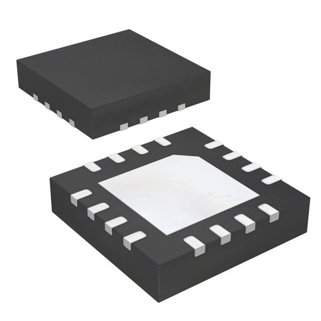


 工商网监
湘ICP备2023018690号
工商网监
湘ICP备2023018690号
