Differential-to-0.7V Differential PCI Express™
Jitter Attenuator
ICS871S1022
DATASHEET
Description
Features
IDT’s PLL-based clock generators offer sub-picosecond jitter,
low-skew clock outputs, and edge rates that meet the ever-growing
demands of today’s networking solutions.
•
•
•
Four 0.7V differential output pairs
•
Crystal oscillator interface designed for 25MHz, 18pF parallel
resonant crystal
•
RMS phase jitter at 100MHz, using a 25MHz crystal
(12kHz – 20MHz): 0.608ps (typical)
•
High frequency jitter attenuator mode has high PLL bandwidth
which allows for better input tracking
•
•
•
•
•
Supports PCI Express Spread-Spectrum Clocking
The ICS871S1022 is a PLL-based clock generator specifically
designed for PCI Express Clock Generation applications. The device
generates 100MHz, 125MHz, 250MHz or 500MHz from either a
25MHz fundamental mode crystal or a 100MHz recovered clock.
The ICS871S1022 has two modes of operation: (1) high frequency
jitter attenuator and (2) high performance clock synthesizer mode.
When in jitter attenuator mode, the ICS871S1022 is able to both
suppress high frequency noise components and function as a
frequency translator. Designed to receive a jittery and noisy clock
from an external source, the ICS871S1022 uses FemtoClock®
technology to clean up the incoming clock and translate the
frequency to one of the four common PCI Express frequencies.
When in synthesizer mode, the device is able to generate high
performance SSC and non-SSC clocks from a low cost external,
25MHz, fundamental mode crystal.
The ICS871S1022 uses FemtoClock® technology to generate low
noise clock outputs capable of providing the seed frequencies for the
common PCI Express link rates.
One differential clock input pair
CLK, nCLK pair can accept the following differential
input levels: LVPECL, LVDS, LVHSTL, HCSL
PCI Express Gen 1, 2 and 3 jitter compliant
3.3V operating supply voltage
0°C to 70°C ambient operating temperature
Available in lead-free (RoHS 6) package
Pin Assignment
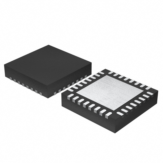
32-Lead VFQFN
5mm x 5mm x 0.925mm package body
K Package
Top View
ICS871S1022EK November 2, 2017
1
©2017 Integrated Device Technology, Inc.
�ICS871S1022 Datasheet
DIFFERENTIAL-TO-0.7V DIFFERENTIAL PCI EXPRESS™ JITTER ATTENUATOR
Block Diagram
100MHz
ICS871S1022EK November 2, 2017
2
©2017 Integrated Device Technology, Inc.
�ICS871S1022 Datasheet
DIFFERENTIAL-TO-0.7V DIFFERENTIAL PCI EXPRESS™ JITTER ATTENUATOR
Table 1. Pin Descriptions
Number
Name
Type
Description
1, 17
VDD
Power
2
CLK
Input
Pulldown
Non-inverting differential clock input.
3
nCLK
Input
Pullup/
Pulldown
Inverting differential clock input. Internal resistor bias to VDD/2.
4
VDD_XTAL
Power
5,
6
XTAL_IN,
XTAL_OUT
Input
7
CLK_SEL
Input
8, 12, 20, 28
GND
Power
Power supply ground.
9, 16, 25, 32
VDDO
Power
Output power supply pins.
10, 11
QB0, nQB0
Output
13
OEB
Input
14,15
QB1, nQB1
Output
18, 19
N1, N0
Input
21
VDDA
Power
Core supply pins.
Crystal oscillator supply pin.
Parallel resonant crystal interface. XTAL_OUT is the output, XTAL_IN is the
input. XTAL_IN is also the overdrive pin if you want to overdrive the crystal
circuit with a single-ended or differential reference clock.
Input source control pin and device operation control pin. See Table 3C.
LVCMOS/LVTTL interface levels.
Pullup
Differential output pair. HCSL interface levels.
Output enable pin for QB, nQB[0:1] pins. When HIGH, the outputs are active.
When LOW, the outputs are in high-impedance state. See Table 3A.
LVCMOS/LVTTL interface levels.
Pullup
Differential output pair. HCSL interface levels.
Pulldown
Output divider control pins. See Table 3D for additional information.
LVCMOS/LVTTL interface levels.
Analog supply pin.
22
SSC_EN
Input
Pulldown
23
PLL_SEL
Input
Pullup
24
IREF
Output
HCSL current reference resistor output. An external fixed precision resistor
(475) from this pin to ground provides a reference current used for
differential current-mode Qx, nQx clock outputs.
26, 27
nQA1, QA1
Output
Differential output pair. HCSL interface levels.
29
OEA
Input
30, 31
nQA0, QA0
Output
Pullup
SSC enable pin. See Table 3B. LVCMOS/LVTTL interface levels.
PLL Bypass control pin. LVCMOS/LVTTL interface levels.
Output enable pin for QA, nQA[0:1] pins. When HIGH, the outputs are active.
When LOW, the outputs are in a high-impedance state. See Table 3A.
LVCMOS/LVTTL interface levels.
Differential output pair. HCSL interface levels.
NOTE: Pullup and Pulldown refer to internal input resistors. See Table 2, Pin Characteristics, for typical values.
Table 2. Pin Characteristics
Symbol
Parameter
CIN
Input Capacitance
5
pF
RPULLUP
Input Pullup Resistor
51
k
RPULLDOWN
Input Pulldown Resistor
51
k
ICS871S1022EK November 2, 2017
Test Conditions
3
Minimum
Typical
Maximum
Units
©2017 Integrated Device Technology, Inc.
�ICS871S1022 Datasheet
DIFFERENTIAL-TO-0.7V DIFFERENTIAL PCI EXPRESS™ JITTER ATTENUATOR
Function Tables
Table 3A. PLL_SEL Function Table
Inputs
Reference
Mode
0
PLL_SEL
Bypass
1
PLL_SEL
PLL
Table 3B. Output Enable Function Table
Inputs
Outputs
OEA, OEB
QA[0:1], nQA[0:1]
QB[0:1], nQB[0:1]
0
High-Impedance
High-Impedance
1
Enabled
Enabled
Table 3C. SSC Enable Function Table
Inputs
Outputs
SSC_EN
Qx[0:1], nQx[0:1]
0
SSC Disabled
1
-0.37% downspread
Table 3D. CLK_SEL Function Table
Input
CLK_SEL
Reference
Mode
0
CLK, nCLK
High Frequency Jitter Attenuator
1
XTAL_IN, XTAL_OUT
Clock Synthesizer
Table 3E. Output Frequency Configuration Table
Inputs
Output Frequency (MHz)
CLK_SEL
Input Frequency (MHz)
N1:N0
N Divider Value
PLL_SEL = 1
PLL_SEL = 0
0
100
00
5
100
20
0
100
01
4
125
25
0
100
10
2
250
50
0
100
11
1
500
100
1
25
00
5
100
5
1
25
01
4
125
6.25
1
25
10
2
250
12.5
1
25
11
1
500
25
ICS871S1022EK November 2, 2017
4
©2017 Integrated Device Technology, Inc.
�ICS871S1022 Datasheet
DIFFERENTIAL-TO-0.7V DIFFERENTIAL PCI EXPRESS™ JITTER ATTENUATOR
Absolute Maximum Ratings
NOTE: Stresses beyond those listed under Absolute Maximum Ratings may cause permanent damage to the device.
These ratings are stress specifications only. Functional operation of product at these conditions or any conditions beyond
those listed in the DC Characteristics or AC Characteristics is not implied. Exposure to absolute maximum rating conditions for
extended periods may affect product reliability.
Item
Rating
Supply Voltage, VDD
4.6V
Inputs, VI
XTAL_IN
Other Inputs
0V to VDD_XTAL
-0.5V to VDD + 0.5V
Outputs, VO
-0.5V to VDDO + 0.5V
Package Thermal Impedance, JA
39.5C/W (0 mps)
Storage Temperature, TSTG
-65C to 150C
DC Electrical Characteristics
Table 4A. Power Supply DC Characteristics, VDD = VDD_XTAL = VDDO = 3.3V ± 5%, TA = 0°C to 70°C
Symbol
Parameter
VDD
Test Conditions
Minimum
Typical
Maximum
Units
Core Supply Voltage
3.135
3.3
3.465
V
VDD_XTAL
Crystal Supply Voltage
3.135
3.3
3.465
V
VDDA
Analog Supply Voltage
VDD – 0.18
3.3
VDD
V
VDDO
Power Supply Voltage
3.135
3.3
3.465
V
IDD
Power Supply Current
100
mA
IDD_XTAL
Crystal Supply Current
7
mA
IDDA
Analog Supply Current
18
mA
IDDO
Output Supply Current
27
mA
Maximum
Units
Table 4B. LVCMOS/LVTTL DC Characteristics, VDD = VDD_XTAL = VDDO = 3.3V ± 5%, TA = 0°C to 70°C
Symbol
Parameter
VIH
Input High Voltage
2.2
VDD + 0.3
V
VIL
Input Low Voltage
-0.3
0.8
V
IIH
Input High Current
IIL
Input Low Current
ICS871S1022EK November 2, 2017
Test Conditions
Minimum
Typical
SSC_EN, N0, N1
VDD = VIN = 3.465V
150
μA
OEA, OEB,
PLL_SEL, CLK_SEL
VDD = VIN = 3.465V
10
μA
SSC_EN, N0, N1
VDD = 3.465V, VIN = 0V
-10
μA
OEA, OEB,
PLL_SEL, CLK_SEL
VDD = 3.465V, VIN = 0V
-150
μA
5
©2017 Integrated Device Technology, Inc.
�ICS871S1022 Datasheet
DIFFERENTIAL-TO-0.7V DIFFERENTIAL PCI EXPRESS™ JITTER ATTENUATOR
Table 4C. Differential DC Characteristics, VDD = VDD_XTAL = VDDO = 3.3V ± 5%, TA = 0°C to 70°C
Symbol
Parameter
Test Conditions
IIH
Input High Current
IIL
Input Low Current
VPP
Peak-to-Peak Voltage; NOTE 1
VCMR
Common Mode Input Voltage; NOTE 1, 2
CLK, nCLK
Minimum
Typical
VDD = VIN = 3.465V
Maximum
Units
150
μA
CLK
VDD = 3.465V, VIN = 0V
-10
μA
nCLK
VDD = 3.465V, VIN = 0V
-150
μA
0.15
1.3
V
GND + 0.5
VDD – 0.85
V
Maximum
Units
NOTE 1: VIL should not be less than -0.3V.
NOTE 2: Common mode input voltage is defined as VIH.
Table 5. Crystal Characteristics
Parameter
Test Conditions
Minimum
Mode of Oscillation
Typical
Fundamental
Frequency
25
MHz
Equivalent Series Resistance (ESR)
50
Shunt Capacitance
7
pF
NOTE: Characterized using an 18pF parallel resonant crystal.
AC Electrical Characteristics
Table 6A. PCI Express Jitter Specifications, VDD = VDD_XTAL = VDDO = 3.3V ± 5%, TA = 0°C to 70°C
Typical
Maximum
PCIe Industry
Specification
Units
ƒ = 100MHz, 25MHz Crystal Input
Evaluation Band: 0Hz - Nyquist
(clock frequency/2), SSC_EN = 0
7.640
11.167
86
ps
tREFCLK_HF_RMS Phase Jitter RMS;
NOTE 2, 4
(PCIe Gen 2)
ƒ = 100MHz, 25MHz Crystal Input
High Band: 1.5MHz - Nyquist
(clock frequency/2), SSC_EN = 0
0.619
1.094
3.1
ps
tREFCLK_LF_RMS
(PCIe Gen 2)
Phase Jitter RMS;
NOTE 2, 4
ƒ = 100MHz, 25MHz Crystal Input
Low Band: 10kHz - 1.5MHz,
SSC_EN = 0
0.084
0.138
3.0
ps
tREFCLK_RMS
(PCIe Gen 3)
Phase Jitter RMS;
NOTE 3, 4
ƒ = 100MHz, 25MHz Crystal Input
Evaluation Band: 0Hz - Nyquist
(clock frequency/2), SSC_EN = 0
0.120
0.241
0.8
ps
Symbol
Parameter
tj
(PCIe Gen 1)
Phase Jitter
Peak-to-Peak;
NOTE 1, 4
Test Conditions
Minimum
NOTE: Electrical parameters are guaranteed over the specified ambient operating temperature range, which is established when the device
is mounted in a test socket with maintained transverse airflow greater than 500 lfpm. The device will meet specifications after thermal
equilibrium has been reached under these conditions. For additional information, refer to the PCI Express Application Note section in the
datasheet.
NOTE 1: Peak-to-Peak jitter after applying system transfer function for the Common Clock Architecture. Maximum limit for PCI Express Gen
1 is 86ps peak-to-peak for a sample size of 106 clock periods.
NOTE 2: RMS jitter after applying the two evaluation bands to the two transfer functions defined in the Common Clock Architecture and
reporting the worst case results for each evaluation band. Maximum limit for PCI Express Generation 2 is 3.1ps RMS for tREFCLK_HF_RMS
(High Band) and 3.0ps RMS for tREFCLK_LF_RMS (Low Band).
NOTE 3: RMS jitter after applying system transfer function for the common clock architecture. This specification is based on the PCI Express
Base Specification Revision 0.7, October 2009 and is subject to change pending the final release version of the specification.
NOTE 4: This parameter is guaranteed by characterization. Not tested in production.
ICS871S1022EK November 2, 2017
6
©2017 Integrated Device Technology, Inc.
�ICS871S1022 Datasheet
DIFFERENTIAL-TO-0.7V DIFFERENTIAL PCI EXPRESS™ JITTER ATTENUATOR
Table 6B. AC Characteristics, VDD = VDD_XTAL = VDDO = 3.3V ± 5%, TA = 0°C to 70°C
Symbol
Parameter
fOUT
Output Frequency
tjit(Ø)
RMS Phase Jitter (Random);
NOTE 1
tsk(o)
Output Skew; NOTE 2, 3
85
ps
tsk(b)
Bank Skew; NOTE 2, 4
30
ps
tjit(cc)
Cycle-to-Cycle Jitter;
NOTE 2, 5
20
ps
tL
PLL Lock Time
100
ms
VMAX
Absolute Max. Output Voltage;
NOTE 6, 7
1150
mV
VMIN
Absolute Min. Output Voltage;
NOTE 6, 8
-300
VRB
Ringback Voltage;
NOTE 9, 10
-100
tSTABLE
Time before VRB is allowed;
Note 9, 10
500
VCROSS
Absolute Crossing Voltage;
NOTE 6, 11, 12
250
VCROSS
Total Variation of VCROSS over
all edges;
NOTE 6, 11, 13
odc
Test Conditions
Minimum
Typical
100
CLK_SEL = 1
100MHz,
Integration Range (12kHz to 20MHz)
Maximum
Units
500
MHz
0.608
CLK_SEL = 1, SSC_EN = 0
ps
mV
100
mV
ps
550
mV
140
mV
Rising Edge Rate; Note 9, 14
0.6
4
V/ns
Falling Edge Rate; Note 9, 14
0.6
4
V/ns
fOUT 250MHz
48
52
%
fOUT = 500MHz
46
54
%
Output Duty Cycle; NOTE 9
NOTE: Electrical parameters are guaranteed over the specified ambient operating temperature range, which is established when the device
is mounted in a test socket with maintained transverse airflow greater than 500 lfpm. The device will meet specifications after thermal
equilibrium has been reached under these conditions.
NOTE 1. Refer to Phase Noise Plot section.
NOTE 2: This parameter is defined in accordance with JEDEC Standard 65.
NOTE 3: Defined as skew between outputs at the same supply voltage and with equal load conditions. Measured at the output differential
cross points.
NOTE 4. Defined as skew within a bank of outputs at the same voltage and with equal load conditions.
NOTE 5. Jitter performance using XTAL inputs.
NOTE 6: Measurement taken from a single ended waveform.
NOTE 7: Defined as the maximum instantaneous voltage including overshoot. See Parameter Measurement Information Section.
NOTE 8: Defined as the minimum instantaneous voltage including undershoot. See Parameter Measurement Information Section
NOTE 9: Measurement taken from a differential waveform.
NOTE 10:TSTABLE is the time the differential clock must maintain a minimum +- 150 mV differential voltage after rising/falling edges before it
is allowed to drop back into the VRB ±100 mV differential range.
NOTE 11: Measured at crossing point where the instantaneous voltage value of the rising edge of CLK+ equals the falling edge of CLK-.
NOTE 12: Refers to the total variation from the lowest crossing point to the highest, regardless of which edge is crossing. Refers to all crossing
points for this measurement.
NOTE 13: Defined as the total variation of all crossing voltages of rising CLK+ and falling CLK-, This is the maximum allowed variance in
Vcross for any particular system. See Parameter Measurement Information Section
NOTE 14: Measured from -150mV to +150mV on the differential waveform (derived from Q minus nQ). The signal must be monotonic through
the measurement region for rise and fall time. The 300mV measurement window is centered on the differential zero crossing.
ICS871S1022EK November 2, 2017
7
©2017 Integrated Device Technology, Inc.
�ICS871S1022 Datasheet
DIFFERENTIAL-TO-0.7V DIFFERENTIAL PCI EXPRESS™ JITTER ATTENUATOR
Noise Power dBc
Hz
Typical Phase Noise at 100MHz
Offset Frequency (Hz)
ICS871S1022EK November 2, 2017
8
©2017 Integrated Device Technology, Inc.
�ICS871S1022 Datasheet
DIFFERENTIAL-TO-0.7V DIFFERENTIAL PCI EXPRESS™ JITTER ATTENUATOR
Parameter Measurement Information
3.3V±5%
3.3V±5%
3.3V±5%
VCC,
VDD,
VDD_XTAL
VDDO
VDDA
33
100
Measurement
Point
100
Measurement
Point
49.9
33
GND
VDD,
VDD,_XTAL
VDDO
VDDA
2pF
49.9
2pF
475
This load condition is used for IDD, tjit(cc), tjit(Ø, tsk(b)) and tsk(o)
measurements.
3.3V HCSL Output Load AC Test Circuit
3.3V HCSL Output Load AC Test Circuit
VDD
nQA0, nQA1,
nQB0, nQB1
nCLK
V
Cross Points
PP
QA0, QA1,
QB0, QB1
V
tcycle n
CMR
CLK
tcycle n+1
tjit(cc) = |tcycle n – tcycle n+1|
1000 Cycles
GND
Differential Input Level
Cycle-to-Cycle Jitter
nQx0, nQx1
nQx
Qx0, Qx1
Qx
nQx0, nQx1
nQy
Qx0, Qx1
Qy
tsk(b)
Where x denotes outputs in the same bank.
Output Skew
Bank Skew
ICS871S1022EK November 2, 2017
9
©2017 Integrated Device Technology, Inc.
�ICS871S1022 Datasheet
DIFFERENTIAL-TO-0.7V DIFFERENTIAL PCI EXPRESS™ JITTER ATTENUATOR
Parameter Measurement Information, continued
Differential Measurement Points for Rise/Fall Edge Rate
RMS Phase Jitter
TSTABLE
VRB
+150mV
VRB = +100mV
0.0V
VRB = -100mV
-150mV
Q - nQ
VRB
TSTABLE
Differential Measurement Points for Duty Cycle/Period
Differential Measurement Points for Ringback
Single-ended Measurement Points for Absolute Cross
Point and Swing
Single-ended Measurement Points for Delta Cross Point
ICS871S1022EK November 2, 2017
10
©2017 Integrated Device Technology, Inc.
�ICS871S1022 Datasheet
DIFFERENTIAL-TO-0.7V DIFFERENTIAL PCI EXPRESS™ JITTER ATTENUATOR
Parameter Measurement Information, continued
PLL Lock Time
Applications Information
Wiring the Differential Input to Accept Single-Ended Levels
line impedance. For most 50 applications, R3 and R4 can be 100.
The values of the resistors can be increased to reduce the loading for
slower and weaker LVCMOS driver. When using single-ended
signaling, the noise rejection benefits of differential signaling are
reduced. Even though the differential input can handle full rail
LVCMOS signaling, it is recommended that the amplitude be
reduced. The datasheet specifies a lower differential amplitude,
however this only applies to differential signals. For single-ended
applications, the swing can be larger, however VIL cannot be less
than -0.3V and VIH cannot be more than VDD + 0.3V. Though some
of the recommended components might not be used, the pads
should be placed in the layout. They can be utilized for debugging
purposes. The datasheet specifications are characterized and
guaranteed by using a differential signal.
Figure 1 shows how a differential input can be wired to accept single
ended levels. The reference voltage VREF = VDD/2 is generated by
the bias resistors R1 and R2. The bypass capacitor (C1) is used to
help filter noise on the DC bias. This bias circuit should be located as
close to the input pin as possible. The ratio of R1 and R2 might need
to be adjusted to position the VREF in the center of the input voltage
swing. For example, if the input clock swing is 2.5V and VDD = 3.3V,
R1 and R2 value should be adjusted to set VREF at 1.25V. The values
below are for when both the single ended swing and VDD are at the
same voltage. This configuration requires that the sum of the output
impedance of the driver (Ro) and the series resistance (Rs) equals
the transmission line impedance. In addition, matched termination at
the input will attenuate the signal in half. This can be done in one of
two ways. First, R3 and R4 in parallel should equal the transmission
Figure 1. Recommended Schematic for Wiring a Differential Input to Accept Single-ended Levels
ICS871S1022EK November 2, 2017
11
©2017 Integrated Device Technology, Inc.
�ICS871S1022 Datasheet
DIFFERENTIAL-TO-0.7V DIFFERENTIAL PCI EXPRESS™ JITTER ATTENUATOR
Differential Clock Input Interface
with the vendor of the driver component to confirm the driver
termination requirements. For example, in Figure 2A, the input
termination applies for IDT open emitter LVHSTL drivers. If you are
using an LVHSTL driver from another vendor, use their termination
recommendation.
The CLK /nCLK accepts LVDS, LVPECL, LVHSTL, HCSL and other
differential signals. Both differential signals must meet the VPP and
VCMR input requirements. Figures 2A to 2E show interface examples
for the CLK/nCLK input driven by the most common driver types. The
input interfaces suggested here are examples only. Please consult
3.3V
1.8V
Zo = 50Ω
CLK
Zo = 50Ω
nCLK
Differential
Input
LVHSTL
IDT
LVHSTL Driver
R1
50Ω
R2
50Ω
Figure 2A. CLK/nCLK Input Driven by an IDT Open
Emitter LVHSTL Driver
Figure 2B. CLK/nCLK Input Driven by a
3.3V LVPECL Driver
Figure 2C. CLK/nCLK Input Driven by a
3.3V LVPECL Driver
Figure 2D. CLK/nCLK Input Driven by a 3.3V LVDS Driver
3.3V
3.3V
*R3
CLK
nCLK
HCSL
*R4
Differential
Input
Figure 2E. CLK/nCLK Input Driven by a
3.3V HCSL Driver
ICS871S1022EK November 2, 2017
12
©2017 Integrated Device Technology, Inc.
�ICS871S1022 Datasheet
DIFFERENTIAL-TO-0.7V DIFFERENTIAL PCI EXPRESS™ JITTER ATTENUATOR
VFQFN EPAD Thermal Release Path
and dependent upon the package power dissipation as well as
electrical conductivity requirements. Thus, thermal and electrical
analysis and/or testing are recommended to determine the minimum
number needed. Maximum thermal and electrical performance is
achieved when an array of vias is incorporated in the land pattern. It
is recommended to use as many vias connected to ground as
possible. It is also recommended that the via diameter should be 12
to 13mils (0.30 to 0.33mm) with 1oz copper via barrel plating. This is
desirable to avoid any solder wicking inside the via during the
soldering process which may result in voids in solder between the
exposed pad/slug and the thermal land. Precautions should be taken
to eliminate any solder voids between the exposed heat slug and the
land pattern. Note: These recommendations are to be used as a
guideline only. For further information, please refer to the Application
Note on the Surface Mount Assembly of Amkor’s Thermally/
Electrically Enhance Leadframe Base Package, Amkor Technology.
In order to maximize both the removal of heat from the package and
the electrical performance, a land pattern must be incorporated on
the Printed Circuit Board (PCB) within the footprint of the package
corresponding to the exposed metal pad or exposed heat slug on the
package, as shown in Figure 3. The solderable area on the PCB, as
defined by the solder mask, should be at least the same size/shape
as the exposed pad/slug area on the package to maximize the
thermal/electrical performance. Sufficient clearance should be
designed on the PCB between the outer edges of the land pattern
and the inner edges of pad pattern for the leads to avoid any shorts.
While the land pattern on the PCB provides a means of heat transfer
and electrical grounding from the package to the board through a
solder joint, thermal vias are necessary to effectively conduct from
the surface of the PCB to the ground plane(s). The land pattern must
be connected to ground through these vias. The vias act as “heat
pipes”. The number of vias (i.e. “heat pipes”) are application specific
PIN
PIN PAD
SOLDER
SOLDER
EXPOSED HEAT SLUG
GROUND PLANE
LAND PATTERN
(GROUND PAD)
THERMAL VIA
PIN
PIN PAD
Figure 3. P.C. Assembly for Exposed Pad Thermal Release Path – Side View (drawing not to scale)
Recommendations for Unused Input and Output Pins
Inputs:
Outputs:
CLK/nCLK Inputs
Differential Outputs
For applications not requiring the use of the differential input, both
CLK and nCLK can be left floating. Though not required, but for
additional protection, a 1k resistor can be tied from CLK to ground.
All unused differential outputs can be left floating. We recommend
that there is no trace attached. Both sides of the differential output
pair should either be left floating or terminated.
LVCMOS Control Pins
All control pins have internal pullups or pulldowns; additional
resistance is not required but can be added for additional protection.
A 1k resistor can be used.
ICS871S1022EK November 2, 2017
13
©2017 Integrated Device Technology, Inc.
�ICS871S1022 Datasheet
DIFFERENTIAL-TO-0.7V DIFFERENTIAL PCI EXPRESS™ JITTER ATTENUATOR
Recommended Termination
types. All traces should be 50Ω impedance single-ended or 100Ω
differential.
Figure 4A is the recommended source termination for applications
where the driver and receiver will be on a separate PCBs. This
termination is the standard for PCI Express™ and HCSL output
Figure 4A. Recommended Source Termination (where the driver and receiver will be on separate PCBs)
be minimized. In addition, a series resistor (Rs) at the driver offers
flexibility and can help dampen unwanted reflections. The optional
resistor can range from 0Ω to 33Ω. All traces should be 50Ω
impedance single-ended or 100Ω differential.
Figure 4B is the recommended termination for applications where a
point-to-point connection can be used. A point-to-point connection
contains both the driver and the receiver on the same PCB. With a
matched termination at the receiver, transmission-line reflections will
Figure 4B. Recommended Termination (where a point-to-point connection can be used)
ICS871S1022EK November 2, 2017
14
©2017 Integrated Device Technology, Inc.
�ICS871S1022 Datasheet
DIFFERENTIAL-TO-0.7V DIFFERENTIAL PCI EXPRESS™ JITTER ATTENUATOR
PCI Express Application Note
PCI Express jitter analysis methodology models the system
response to reference clock jitter. The block diagram below shows
the most frequently used Common Clock Architecture in which a
copy of the reference clock is provided to both ends of the PCI
Express Link.
In the jitter analysis, the transmit (Tx) and receive (Rx) serdes PLLs
are modeled as well as the phase interpolator in the receiver. These
transfer functions are called H1, H2, and H3 respectively. The overall
system transfer function at the receiver is:
Ht s = H3 s H1 s – H2 s
The jitter spectrum seen by the receiver is the result of applying this
system transfer function to the clock spectrum X(s) and is:
Y s = X s H3 s H1 s – H2 s
PCIe Gen 2A Magnitude of Transfer Function
In order to generate time domain jitter numbers, an inverse Fourier
Transform is performed on X(s)*H3(s) * [H1(s) - H2(s)].
PCI Express Common Clock Architecture
For PCI Express Gen 1, one transfer function is defined and the
evaluation is performed over the entire spectrum: DC to Nyquist (e.g
for a 100MHz reference clock: 0Hz – 50MHz) and the jitter result is
reported in peak-peak.
PCIe Gen 2B Magnitude of Transfer Function
For PCI Express Gen 3, one transfer function is defined and the
evaluation is performed over the entire spectrum. The transfer
function parameters are different from Gen 1 and the jitter result is
reported in RMS.
PCIe Gen 1 Magnitude of Transfer Function
PCIe Gen 3 Magnitude of Transfer Function
For PCI Express Gen 2, two transfer functions are defined with 2
evaluation ranges and the final jitter number is reported in rms. The
two evaluation ranges for PCI Express Gen 2 are 10kHz – 1.5MHz
(Low Band) and 1.5MHz – Nyquist (High Band). The plots show the
individual transfer functions as well as the overall transfer function Ht.
ICS871S1022EK November 2, 2017
For a more thorough overview of PCI Express jitter analysis
methodology, please refer to IDT Application Note PCI Express
Reference Clock Requirements.
15
©2017 Integrated Device Technology, Inc.
�ICS871S1022 Datasheet
DIFFERENTIAL-TO-0.7V DIFFERENTIAL PCI EXPRESS™ JITTER ATTENUATOR
Schematic Example
0.1μF capacitor in each power pin filter should be placed on the
device side of the PCB and the other components can be placed on
the opposite side.
Figure 5 shows an example of ICS871S1022 application schematic.
In this example, the device is operated VDD= VDDO = VDD_XTAL = VDDA =
3.3V. An 18pF parallel resonant 25MHz crystal is used. The load
capacitance C1 = 27pF and C2 = 27pF are recommended for
frequency accuracy. Depending on the parasitic of the printed circuit
board layout, these values might require a slight adjustment to
optimize the frequency accuracy. Crystals with other load
capacitance specifications can be used. This will require adjusting C1
and C2. For this device, the crystal load capacitors are required for
proper operation.
Power supply filter recommendations are a general guideline to be
used for reducing external noise from coupling into the devices. The
filter performance is designed for wide range of noise frequency. This
low-pass filter starts to attenuate noise at approximately 10 kHz. If a
specific frequency noise component with high amplitude interference
is known, such as switching power supplies frequencies, it is
recommended that component values be adjusted and if required,
additional filtering be added. Additionally general design practice for
power plane voltage stability suggests adding bulk capacitances in
the general area of all devices.
As with any high speed analog circuitry, the power supply pins are
vulnerable to random noise. To achieve optimum jitter performance,
power supply isolation is required. The ICS871S1022 provides
separate power supplies to isolate noise from coupling into the
internal PLL.
The schematic example focuses on functional connections and is not
configuration specific. Refer to the pin description and functional
tables in the datasheet to ensure the logic control inputs are properly
set.
In order to achieve the best possible filtering, it is recommended that
the placement of the filter components be on the device side of the
PCB as close to the power pins as possible. If space is limited, the
Figure 5. ICS871S1022 Schematic Example
ICS871S1022EK November 2, 2017
16
©2017 Integrated Device Technology, Inc.
�ICS871S1022 Datasheet
DIFFERENTIAL-TO-0.7V DIFFERENTIAL PCI EXPRESS™ JITTER ATTENUATOR
Power Considerations
This section provides information on power dissipation and junction temperature for the ICS871S1022.
Equations and example calculations are also provided.
1.
Power Dissipation.
The total power dissipation for the ICS871S1022 is the sum of the core power plus the power dissipated in the load(s).
The following is the power dissipation for VDD = 3.3V + 5% = 3.465V, which gives worst case results.
NOTE: Please refer to Section 3 for details on calculating power dissipated in the load.
The maximum current at 70°C is as follows:
IDD_MAX = 87mA
IDD_XTAL_MAX = 7mA
IDDA_MAX = 18mA
IDDO_MAX = 27mA
Power (no-load)MAX = VDD_MAX * (IDD_MAX + IDD_XTAL + IDDA_MAX + IDDO_MAX) = 3.465V *(87mA + 7mA + 18mA + 27mA) = 481.635mW
•
Power (outputs)MAX = 44.5mW/Loaded Output pair
If all outputs are loaded, the total power is 4 * 44.5mW = 178mW
Total Power_MAX = 481.635mW + 178mW = 659.635mW
2. Junction Temperature.
Junction temperature, Tj, is the temperature at the junction of the bond wire and bond pad directly affects the reliability of the device. The
maximum recommended junction temperature is 125°C. Limiting the internal transistor junction temperature, Tj, to 125°C ensures that the bond
wire and bond pad temperature remains below 125°C.
The equation for Tj is as follows: Tj = JA * Pd_total + TA
Tj = Junction Temperature
JA = Junction-to-Ambient Thermal Resistance
Pd_total = Total Device Power Dissipation (example calculation is in section 1 above)
TA = Ambient Temperature
In order to calculate junction temperature, the appropriate junction-to-ambient thermal resistance JA must be used. Assuming no air flow and
a multi-layer board, the appropriate value is 39.5°C/W per Table 7 below.
Therefore, Tj for an ambient temperature of 70°C with all outputs switching is:
70°C + 0.660W *39.5°C/W = 96.1°C. This is below the limit of 125°C.
This calculation is only an example. Tj will obviously vary depending on the number of loaded outputs, supply voltage, air flow and the type of
board (multi-layer).
Table 7. Thermal Resistance JA for 32 Lead VFQFN, Forced Convection
JA vs. Air Flow
Meters per Second
Multi-Layer PCB, JEDEC Standard Test Boards
ICS871S1022EK November 2, 2017
0
39.5°C/W
17
34.5°C/W
31.0°C/W
©2017 Integrated Device Technology, Inc.
�ICS871S1022 Datasheet
DIFFERENTIAL-TO-0.7V DIFFERENTIAL PCI EXPRESS™ JITTER ATTENUATOR
3. Calculations and Equations.
The purpose of this section is to calculate power dissipation on the IC per HCSL output pair.
HCSL output driver circuit and termination are shown in Figure 6.
VDDO
IOUT = 17mA
➤
VOUT
RREF =
475Ω ± 1%
RL
50Ω
IC
Figure 6. HCSL Driver Circuit and Termination
HCSL is a current steering output which sources a maximum of 17mA of current per output. To calculate worst case on-chip power dissipation,
use the following equations which assume a 50 load to ground.
The highest power dissipation occurs when VDDO_MAX.
Power
= (VDDO_MAX – VOUT) * IOUT,
since VOUT – IOUT * RL
= (VDDO_MA – IOUT * RL) * IOUT
= (3.465V – 17mA * 50) * 17mA
Total Power Dissipation per output pair = 44.5mW
ICS871S1022EK November 2, 2017
18
©2017 Integrated Device Technology, Inc.
�ICS871S1022 Datasheet
DIFFERENTIAL-TO-0.7V DIFFERENTIAL PCI EXPRESS™ JITTER ATTENUATOR
Reliability Information
Table 8. JA vs. Air Flow Table for a 32 Lead VFQFN
JA vs. Air Flow
Meters per Second
Multi-Layer PCB, JEDEC Standard Test Boards
0
1
2.5
39.5°C/W
34.5°C/W
31.0°C/W
Transistor Count
The transistor count for ICS871S1022 is: 11,517
ICS871S1022EK November 2, 2017
19
©2017 Integrated Device Technology, Inc.
�ICS871S1022 Datasheet
DIFFERENTIAL-TO-0.7V DIFFERENTIAL PCI EXPRESS™ JITTER ATTENUATOR
Package Outline Drawings – Page 1
ICS871S1022EK November 2, 2017
20
©2017 Integrated Device Technology, Inc.
�ICS871S1022 Datasheet
DIFFERENTIAL-TO-0.7V DIFFERENTIAL PCI EXPRESS™ JITTER ATTENUATOR
Package Outline Drawings – Page 2
ICS871S1022EK November 2, 2017
21
©2017 Integrated Device Technology, Inc.
�ICS871S1022 Datasheet
DIFFERENTIAL-TO-0.7V DIFFERENTIAL PCI EXPRESS™ JITTER ATTENUATOR
Ordering Information
Table 9. Ordering Information
Part/Order Number
871S1022EKLF
871S1022EKLFT
Marking
ICS1S1022EL
ICS1S1022EL
Package
“Lead-Free” 32 Lead VFQFN
“Lead-Free” 32 Lead VFQFN
Shipping Packaging
Tray
2500 Tape & Reel
Temperature
0C to 70C
0C to 70C
NOTE: Parts that are ordered with an “LF” suffix to the part number are the Pb-Free configuration and are RoHS compliant.
Revision History
Revision Date
Description of Change
• Added Table 3A
November 2, 2017
• Updated Table 3E
• Updated the package outline drawings; however, no technical changes
August 24, 2011
AC Characteristics Table - changed IDD max from 87mA to 100mA (per Errata NEN-11-08.
Power Considerations - added maximum current note.
Corporate Headquarters
Sales
Tech Support
6024 Silver Creek Valley Road
San Jose, CA 95138 USA
www.IDT.com
1-800-345-7015 or 408-284-8200
Fax: 408-284-2775
www.IDT.com/go/sales
www.IDT.com/go/support
DISCLAIMER Integrated Device Technology, Inc. (IDT) and its affiliated companies (herein referred to as “IDT”) reserve the right to modify the products and/or specifications described herein at any time, without
notice, at IDT’s sole discretion. Performance specifications and operating parameters of the described products are determined in an independent state and are not guaranteed to perform the same way when
installed in customer products. The information contained herein is provided without representation or warranty of any kind, whether express or implied, including, but not limited to, the suitability of IDT's products
for any particular purpose, an implied warranty of merchantability, or non-infringement of the intellectual property rights of others. This document is presented only as a guide and does not convey any license under
intellectual property rights of IDT or any third parties.
IDT's products are not intended for use in applications involving extreme environmental conditions or in life support systems or similar devices where the failure or malfunction of an IDT product can be reasonably
expected to significantly affect the health or safety of users. Anyone using an IDT product in such a manner does so at their own risk, absent an express, written agreement by IDT.
Integrated Device Technology, IDT and the IDT logo are trademarks or registered trademarks of IDT and its subsidiaries in the United States and other countries. Other trademarks used herein are the property of
IDT or their respective third party owners. For datasheet type definitions and a glossary of common terms, visit www.idt.com/go/glossary. Integrated Device Technology, Inc.. All rights reserved.
ICS871S1022EK November 2, 2017
22
©2017 Integrated Device Technology, Inc.
�IMPORTANT NOTICE AND DISCLAIMER
RENESAS ELECTRONICS CORPORATION AND ITS SUBSIDIARIES (“RENESAS”) PROVIDES TECHNICAL
SPECIFICATIONS AND RELIABILITY DATA (INCLUDING DATASHEETS), DESIGN RESOURCES (INCLUDING
REFERENCE DESIGNS), APPLICATION OR OTHER DESIGN ADVICE, WEB TOOLS, SAFETY INFORMATION, AND
OTHER RESOURCES “AS IS” AND WITH ALL FAULTS, AND DISCLAIMS ALL WARRANTIES, EXPRESS OR IMPLIED,
INCLUDING, WITHOUT LIMITATION, ANY IMPLIED WARRANTIES OF MERCHANTABILITY, FITNESS FOR A
PARTICULAR PURPOSE, OR NON-INFRINGEMENT OF THIRD PARTY INTELLECTUAL PROPERTY RIGHTS.
These resources are intended for developers skilled in the art designing with Renesas products. You are solely responsible
for (1) selecting the appropriate products for your application, (2) designing, validating, and testing your application, and (3)
ensuring your application meets applicable standards, and any other safety, security, or other requirements. These
resources are subject to change without notice. Renesas grants you permission to use these resources only for
development of an application that uses Renesas products. Other reproduction or use of these resources is strictly
prohibited. No license is granted to any other Renesas intellectual property or to any third party intellectual property.
Renesas disclaims responsibility for, and you will fully indemnify Renesas and its representatives against, any claims,
damages, costs, losses, or liabilities arising out of your use of these resources. Renesas' products are provided only subject
to Renesas' Terms and Conditions of Sale or other applicable terms agreed to in writing. No use of any Renesas resources
expands or otherwise alters any applicable warranties or warranty disclaimers for these products.
(Rev.1.0 Mar 2020)
Corporate Headquarters
Contact Information
TOYOSU FORESIA, 3-2-24 Toyosu,
Koto-ku, Tokyo 135-0061, Japan
www.renesas.com
For further information on a product, technology, the most
up-to-date version of a document, or your nearest sales
office, please visit:
www.renesas.com/contact/
Trademarks
Renesas and the Renesas logo are trademarks of Renesas
Electronics Corporation. All trademarks and registered
trademarks are the property of their respective owners.
© 2020 Renesas Electronics Corporation. All rights reserved.
�