873991
LOW VOLTAGE, LVCMOS/
LVPECL-TO-LVPECL/ECL CLOCK GENERATOR
GENERAL DESCRIPTION
FEATURES
The 873991 is a low voltage, low skew, 3.3V LVPECL
or ECL Clock Generator . The 873991 has two selectable
clock inputs. The PCLK, nPCLK pair can accept an LVPECL
input and the TEST_CLK pin can accept a LVCMOS or LVTTL input. This device has a fully integrated PLL along with
frequency configurable outputs. An external feedback input and
output regenerates clocks with “zero delay”.
• 14 differential LVPECL outputs
The four independent banks of outputs each have their
own output dividers, which allow the device to generate a
multitude of different bank frequency ratios and output-toinput frequency ratios. The output frequency range is 25MHz to
400MHz and the input frequency range is 6.25MHz to 125MHz.
The PLL_SEL input can be used to bypass the PLL for test
and system debug purposes. In bypass mode, the input clock
is routed around the PLL and into the internal output dividers.
• Input frequency range: 6.25MHz to 125MHz
• Selectable differential LVPECL or TEST_CLK inputs
• PCLK, nPCLK can accept the following input levels:
LVPECL, CML, SSTL
• TEST_CLK accepts the following input levels:
LVCMOS, LVTTL
• Output frequency: 400MHz (maximum)
• VCO range: 200MHz to 800MHz
• Output skew: 250ps (maximum)
• Cycle-to-cyle jitter: ±50ps (typical)
• LVPECL mode operating voltage supply range:
VCC = 3.135V to 3.465V, VEE = 0V
The 873991 also has a SYNC output which can be used for
system synchronization purposes. It monitors Bank A and Bank
C outputs for coincident rising edges and signals a pulse per the
timing diagrams in this data sheet. This feature is used primarily
in applications where Bank A and Bank C are running at different
frequencies, and is particularly useful when they are running at
non-integer multiples of each other.
• ECL mode operating voltage supply range:
VCC = 0V, VEE = -3.465V to -3.135V
• 0°C to 70°C ambient operating temperature
• Industrial temperature available upon request
• Lead-Free package fully RoHS compliant
Example Applications:
• Use replacement part 873996AYLF
1. Line Card Multiplier: Multiply 19.44MHz from a back-plane
to 77.76MHz on the line card ASIC and Serdes.
PIN ASSIGNMENT
2. Zero Delay Buffer: Fan out up to thirteen 100MHz copies
from a reference clock to multiple processing units on an
embedded system.
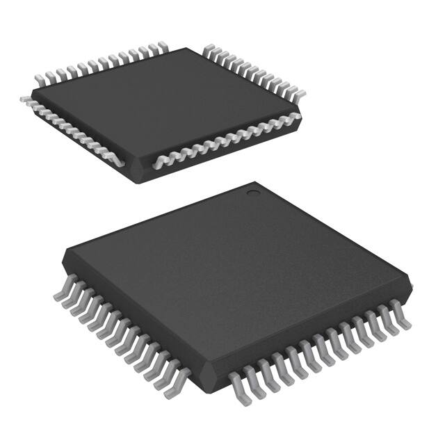
52-Lead LQFP
10mm x 10mm x 1.4mm package body
Y package
Top View
873991
REV. A 8/25/15
1
�873991
LOW VOLTAGE, LVCMOS/
LVPECL-TO-LVPECL/ECL CLOCK GENERATOR
BLOCK DIAGRAM
VCO_SEL Pulldown
PLL_EN Pulldown
QA0
nQA0
REF_SEL Pulldown
TEST_CLK Pulldown
nPCLK
QA1
nQA1
PCLK
PHASE
DETECTOR
EXT_FB
QA2
nQA2
VCO
QA3
nQA3
LPF
nEXT_FB
QB0
nQB0
MR Pulldown
QB1
nQB1
FREQUENCY
GENERATOR
FSEL_0:3 Pulldown
SYNC
QB2
nQB2
QB3
nQB3
QC0
FSEL_FB0:2 Pulldown
nQC0
QC1
nQC1
QC2
nQC2
QD0
nQD0
SYNC_SEL Pulldown
QD1
nQD1
QFB
nQFB
873991
REV. A 8/25/15
2
�873991
LOW VOLTAGE, LVCMOS/
LVPECL-TO-LVPECL/ECL CLOCK GENERATOR
TABLE 1. PIN DESCRIPTIONS
Number
Name
1
VEE
Type
Power
Description
Negative supply pin.
Active High Master Reset. When logic HIGH, the internal dividers are
reset causing the true outputs (Qx) to go low and the inverted outputs
Pulldown
(nQx) to go high. When logic LOW, the internal dividers and the outputs
are enabled. LVCMOS/LVTTL interface levels.
PLL enable pin. When logic LOW, PLL is enabled. When logic HIGH, PLL
Pulldown
is in bypass mode. LVCMOS/LVTTL interface levels.
Selects between the different reference inputs as the PLL reference
Pulldown source. When logic LOW, selects PCLK/nPCLK. When logic HIGH, selects
TEST_CLK. LVCMOS/LVTTL interface levels.
2
MR
Input
3
PLL_EN
Input
4
REF_SEL
Input
5
6
7
FSEL_FB2
FSEL_FB1
FSEL_FB0
Input
8
TEST_CLK
Input
Pulldown LVCMOS/LVTTL test clock input.
9
PCLK
Input
Pulldown Non-inverting differential LVPECL clock input.
10
nPCLK
Input
Pullup/
Inverting differential LVPECL clock input. VCC/2 default when left floating.
Pulldown
Pulldown Feedback frequency select pins. LVCMOS/LVTTL interface levels.
11
VCC
Power
12
EXT_FB
Input
Pulldown External feedback input.
Core supply pin.
13
nEXT_FB
Input
Pullup/
External feedback input. t. VCC/2 default when left floating.
Pulldown
14
VCCA
Power
Analog supply pin.
15
16
nQFB
QFB
Output
Differential feedback output pair. LVPECL Interface levels.
17, 22, 30, 42
VCCO
Power
Output supply pins.
18, 19
nQD0, QD0
Output
Differential output pair. LVPECL interface levels.
20, 21
nQD1, QD1
Output
Differential output pair. LVPECL interface levels.
23, 24
nQC0, QC0
Output
Differential output pair. LVPECL interface levels.
25, 26
nQC1, QC1
Output
Differential output pair. LVPECL interface levels.
27
33
36
39
FSEL3
FSEL2
FSEL1
FSEL0
Input
28, 29
nQC2, QC2
Output
Differential output pair. LVPECL interface levels.
31, 32
nQB0, QB0
Output
Differential output pair. LVPECL interface levels.
34, 35
nQB1, QB1
Output
Differential output pair. LVPECL interface levels.
37, 38
nQB2, QB2
Output
Differential output pair. LVPECL interface levels.
40, 41
nQB3, QB3
Output
Differential output pair. LVPECL interface levels.
43, 44
nQA0, QA0
Output
Differential output pair. LVPECL interface levels.
45, 46
nQA1, QA1
Output
Differential output pair. LVPECL interface levels.
47, 48
nQA2, QA2
Output
Differential output pair. LVPECL interface levels.
49, 50
nQA3, QA3
Output
Differential output pair. LVPECL interface levels.
51
SYNC_SEL
Input
Pulldown
52
VCO_SEL
Input
Pulldown Selects VCO range. LVCMOS/LVTTL interface levels.
Pulldown Frequency select pins. LVCMOS/LVTTL interface levels.
SYNC output select pin. When LOW, the SYNC otuput follows the timing
diagram (page 5). When HIGH, QD output follows QC output.
NOTE: Pullup and Pulldown refer to internal input resistors. See Table 2, Pin Characteristics, for typical values.
873991
REV. A 8/25/15
3
�873991
LOW VOLTAGE, LVCMOS/
LVPECL-TO-LVPECL/ECL CLOCK GENERATOR
TABLE 2. PIN CHARACTERISTICS
Symbol
Parameter
Test Conditions
CIN
Input Capacitance
4
pF
RPULLDOWN
Input Pulldown Resistor
51
kΩ
RPULLup
Input Pullup Resistor
51
kΩ
TABLE 3A. SELECT PIN FUNCTION TABLE
Inputs
Minimum
Typical
Maximum
Units
TABLE 3B. FEEDBACK CONTROL FUNCTION TABLE
Inputs
Outputs
Outputs
FSEL3
FSEL2
FSEL1
FSEL0
QAx
QBx
QCx
FSEL_FB2
FSEL_FB1
FSEL_FB0
QFB
0
0
0
0
÷2
÷2
÷2
0
0
0
÷2
0
0
0
1
÷2
÷2
÷4
0
0
1
÷4
0
0
1
0
÷2
÷4
÷4
0
1
0
÷6
1
1
÷8
0
0
1
1
÷2
÷2
÷6
0
0
1
0
0
÷2
÷6
÷6
1
0
0
÷8
0
1
0
1
÷2
÷4
÷6
1
0
1
÷16
0
1
1
0
÷2
÷4
÷8
1
1
0
÷24
0
1
1
1
÷2
÷6
÷8
1
1
1
÷32
1
0
0
0
÷2
÷2
÷8
1
0
0
1
÷2
÷8
÷8
1
0
1
0
÷4
÷4
÷6
1
0
1
1
÷4
÷6
÷6
1
1
0
0
÷4
÷6
÷8
1
1
0
1
÷6
÷6
÷8
1
1
1
0
÷6
÷8
÷8
1
1
1
1
÷8
÷8
÷8
TABLE 3C. INPUT CONTROL FUNCTION TABLE
Control Input Pin
Logic 0
Logic 1
PLL_EN
Enables PLL
Bypasses PLL
VCO_SEL
fVCO
fVCO/2
REF_SEL
Selects PCLK/nPCLK
Selects TEST_CLK
MR
---
Resets outputs
SYNC_SEL
Selects outputs
Match QC Outputs
873991
REV. A 8/25/15
4
�873991
LOW VOLTAGE, LVCMOS/
LVPECL-TO-LVPECL/ECL CLOCK GENERATOR
FIGURE 1. TIMING DIAGRAMS
873991
REV. A 8/25/15
5
�873991
LOW VOLTAGE, LVCMOS/
LVPECL-TO-LVPECL/ECL CLOCK GENERATOR
ABSOLUTE MAXIMUM RATINGS
Supply Voltage, VCC
4.6V
Inputs, VI
-0.5V to VCC + 0.5 V
NOTE: Stresses beyond those listed under Absolute Maximum
Ratings may cause permanent damage to the device. These
ratings are stress specifications only. Functional operation of
product at these conditions or any conditions beyond those listed
in the DC Characteristics or AC Characteristics is not implied.
Exposure to absolute maxi-mum rating conditions for extended
periods may affect product reliability.
Outputs, IO
Continuous Current
Surge Current
50mA
100mA
Package Thermal Impedance, θJA
42.3°C/W (0 lfpm)
Storage Temperature, TSTG
-65°C to 150°C
TABLE 4A. POWER SUPPLY DC CHARACTERISTICS, VCC = VCCA = VCCO = 3.3V ± 5%, VEE = 0V, TA = 0°C TO 70°C
Symbol
Parameter
Minimum
Typical
Maximum
Units
VCC
Core Supply Voltage
Test Conditions
3.135
3.3
3.465
V
VCCA
Analog Supply Voltage
3.135
3.3
3.465
VCCO
Output Supply Voltage
3.135
3.3
3.465
V
ICC
Power Supply Current
150
mA
ICCA
Analog Supply Current
15
mA
ICCO
Output Supply Current
95
mA
TABLE 4B. LVCMOS/LVTTL DC CHARACTERISTICS, VCC = VCCA = VCCO = 3.3V ± 5%, VEE = 0V, TA = 0°C TO 70°C
Symbol
VIH
Parameter
Input High Voltage
Test Conditions
PLL_EN, VCO_SEL,
REF_SEL, SYNC_SEL,
FSEL_FB0:FSEL_FB2,
FSEL0:FSEL3, MR
TEST_CLK
PLL_EN, VCO_SEL,
REF_SEL, SYNC_SEL,
FSEL_FB0:FSEL_FB2,
FSEL0:FSEL3, MR
VIL
Input Low Voltage
IIH
Input High Current
VCC = VIN = 3.465V
IIL
Input Low Current
VIN = 0V, VCC = 3.465V
TEST_CLK
Minimum
Typical
Maximum
Units
2
VCC + 0.3
V
2
VCC + 0.3
V
-0.3
0.8
V
-0.3
1.3
V
150
µA
-5
µA
TABLE 4C. LVPECL DC CHARACTERISTICS, VCC = VCCA = VCCO = 3.3V ± 5%, VEE = 0V, TA = 0°C TO 70°C
Symbol
Parameter
Test Conditions
IIH
Input High Current
IIL
Input Low Current
VPP
Peak-to-Peak Input Voltage
VCMR
Common Mode Input Voltage; NOTE 1, 2
VOH
Output High Voltage; NOTE 3
VOL
Output Low Voltage; NOTE 3
VSWING
Peak-to-Peak Output Voltage Swing
Minimum
Typical
Maximum
Units
PCLK
VCC = VIN = 3.465V
150
µA
nPCLK
VCC = VIN = 3.465V
5
µA
PCLK
VCC = 3.465V, VIN = 0V
-5
µA
nPCLK
VCC = 3.465V, VIN = 0V
-150
µA
0.3
1
V
VEE + 1.5
VCC
V
VCC - 1.4
VCC - 0.9
V
VCC - 2.0
VCC - 1.7
V
0.6
1
V
NOTE 1: Common mode voltage is defined as VIH.
NOTE 2: For single ended applications, the maximum input voltage for PCLK, nPCLK is VCC + 0.3V.
NOTE 3: Outputs terminated with 50Ω to VCCO - 2V. .
873991
REV. A 8/25/15
6
�873991
LOW VOLTAGE, LVCMOS/
LVPECL-TO-LVPECL/ECL CLOCK GENERATOR
TABLE 5. PLL INPUT REFERENCE CHARACTERISTICS, VCC = VCCA = VCCO = 3.3V±5%, TA = 0°C TO 70°C
Symbol
Parameter
tR / tR
Input Rise/Fall Time
Test Conditions
Reference Frequency
VCO_SEL = 0
fREF
Reference Frequency
VCO_SEL = 1
fREFDC
Minimum
Typical
TEST_CLK
Maximum
Units
3
ns
Feedback ÷ 6
66.66
133.33
MHz
Feedback ÷ 8
50
100
MHz
Feedback ÷ 16
25
50
MHz
Feedback ÷ 24
16.66
33.33
MHz
Feedback ÷ 32
12.5
25
MHz
Feedback ÷ 4
50
100
MHz
Feedback ÷ 6
33.33
66.66
MHz
Feedback ÷ 8
25
50
MHz
Feedback ÷ 16
12.5
25
MHz
Feedback ÷ 24
8.33
16.66
MHz
Feedback ÷ 32
6.25
12.5
MHz
25
75
%
Reference Input Duty Cycle
NOTE: These parameters are guaranteed by design, but are not tested in production.
TABLE 6. AC CHARACTERISTICS, VCC = VCCA = VCCO = 3.3V ± 5%, TA = 0°C TO 70°C
Symbol
fMAX
Parameter
Minimum
Typical
Output Frequency
tsk(o)
Static Phase Offset;
PCLK, nPCLK
NOTE 1, 5
Output Skew; NOTE 2, 3
tsk(w)
Multiple Frequency Skew; NOTE 3, 6
tjit(cc)
Cycle-to-Cycle Jitter; NOTE 3
t(Ø)
Test Conditions
fVCO
PLL VCO Lock Range; NOTE 4
tLOCK
PLL Lock Time
tR / t F
Output Rise/Fall Time
odc
Output Duty Cycle
0
170
Maximum
Units
400
MHz
325
ps
250
ps
350
ps
±50
ps
PLL_SEL = 0
400
800
MHz
PLL_SEL = 1
200
400
MHz
10
ms
0.2
1
ns
45
55
%
20% to 80%
All parameters measured at fMAX unless noted otherwise.
NOTE 1: Defined as the time difference between the input reference clock and the average feedback input signal
when the PLL is locked and the input reference frequency is stable.
NOTE 2:Defined as skew between outputs at the same supply voltage and with equal load conditions.
Measured at the output differential cross points.
NOTE 3: This parameter is defined in accordance with JEDEC Standard 65.
NOTE 4: When VCO_SEL = 0, the PLL will be unstable with feedback configurations of ÷2, ÷4 and some ÷6.
When VCO_SEL = 1, the PLL will be unstable with a feedback configuration of ÷2.
NOTE 5: Static phase offset is specified for an input frequency of 50MHz with feedback in ÷8.
NOTE 6: Defined as skew across banks of outputs switching in the same direction operating at different frequencies
with the same supply voltages and equal load conditions. Measured at VCCO/2.
873991
REV. A 8/25/15
7
�873991
LOW VOLTAGE, LVCMOS/
LVPECL-TO-LVPECL/ECL CLOCK GENERATOR
PARAMETER MEASUREMENT INFORMATION
OUTPUT LOAD AC TEST CIRCUIT
DIFFERENTIAL INPUT LEVELS
OUTPUT SKEW
CYCLE-TO-CYCLE JITTER
STATIC PHASE OFFSET
MULTIPLE FREQUENCY SKEW
OUTPUT RISE/FALL TIME
OUTPUT DUTY CYCLE/PULSE WIDTH/PERIOD
873991
REV. A 8/25/15
8
�873991
LOW VOLTAGE, LVCMOS/
LVPECL-TO-LVPECL/ECL CLOCK GENERATOR
APPLICATION INFORMATION
POWER SUPPLY FILTERING TECHNIQUES
As in any high speed analog circuitry, the power supply
pins are vulnerable to random noise. The 873991 provides
separate power supplies to isolate any high switching
noise from the outputs to the internal PLL. VCC, VCCA, and
VCCO should be individually connected to the power supply
plane through vias, and bypass capacitors should be
used for each pin. To achieve optimum jitter performance,
power supply isolation is required. Figure 2 illustrates how
a 10Ω resistor along with a 10μF and a .01μF bypass
capacitor should be connected to each VCCA pin.
3.3V
VCC
.01μF
10Ω
VCCA
.01μF
10μF
FIGURE 2. POWER SUPPLY FILTERING
WIRING THE DIFFERENTIAL INPUT TO ACCEPT SINGLE ENDED LEVELS
Figure 3 shows how the differential input can be wired to accept
single ended levels. The reference voltage V_REF = VCC/2 is
generated by the bias resistors R1, R2 and C1. This bias circuit
should be located as close as possible to the input pin. The ratio
of R1 and R2 might need to be adjusted to position the V_REF
in the center of the input voltage swing. For example, if the input
clock swing is only 2.5V and VCC = 3.3V, V_REF should be 1.25V
and R2/R1 = 0.609.
FIGURE 3. SINGLE ENDED SIGNAL DRIVING DIFFERENTIAL INPUT
873991
REV. A 8/25/15
9
�873991
LOW VOLTAGE, LVCMOS/
LVPECL-TO-LVPECL/ECL CLOCK GENERATOR
TERMINATION FOR 3.3V LVPECL OUTPUTS
The clock layout topology shown below is a typical termination
for LVPECL outputs. The two different layouts mentioned are
recommended only as guidelines.
drive 50Ω transmission lines. Matched impedance techniques
should be used to maximize operating frequency and minimize
signal distortion. Figures 4A and 4B show two different layouts
which are recommended only as guidelines. Other suitable clock
layouts may exist and it would be recommended that the board
designers simulate to guarantee compatibility across all printed
circuit and clock component process variations.
FOUT and nFOUT are low impedance follower outputs that
generate ECL/LVPECL compatible outputs. Therefore, terminating resistors (DC current path to ground) or current sources
must be used for functionality. These outputs are designed to
FIGURE 4A. LVPECL OUTPUT TERMINATION
FIGURE 4B. LVPECL OUTPUT TERMINATION
873991
REV. A 8/25/15
10
�873991
LOW VOLTAGE, LVCMOS/
LVPECL-TO-LVPECL/ECL CLOCK GENERATOR
LVPECL CLOCK INPUT INTERFACE
The PCLK /nPCLK accepts LVPECL, CML, SSTL and other
differential signals. Both VSWING and VOH must meet the VPP
and VCMR input requirements. Figures 5A to 5D show interface
examples for the PCLK/nPCLK input driven by the most
common driver types. The input interfaces suggested here
are examples only. If the driver is from another vendor, use
their termination recommendation. Please consult with the
vendor of the driver component to confirm the driver
termination requirements.
2.5V
3.3V
3.3V
3.3V
CML
Zo = 50 Ohm
R1
50
3.3V
2.5V
R2
50
SSTL
Zo = 60 Ohm
R3
120
R4
120
PCLK
PCLK
Zo = 60 Ohm
Zo = 50 Ohm
nPCLK
nPCLK
HiPerClockS
PCLK/nPCLK
R1
120
FIGURE 5A. PCLK/nPCLK INPUT DRIVEN
BY A CML DRIVER
3.3V
3.3V
Zo = 50 Ohm
R3
125
FIGURE 5B. PCLK/nPCLK INPUT DRIVEN
BY AN SSTL DRIVER
3.3V
3.3V
3.3V
3.3V
R4
125
Zo = 50 Ohm
C1
LVDS
R3
1K
R4
1K
PCLK
PCLK
R5
100
Zo = 50 Ohm
nPCLK
LVPECL
R1
84
HiPerClockS
PCLK/nPCLK
R2
120
C2
nPCLK
Zo = 50 Ohm
HiPerClockS
Input
R1
1K
R2
84
FIGURE 5C. PCLK/nPCLK INPUT DRIVEN
BY A 3.3V LVPECL DRIVER
HiPerClockS
PCLK/nPCLK
R2
1K
FIGURE 5D. PCLK/nPCLK INPUT DRIVEN
BY A 3.3V LVDS DRIVER
873991
REV. A 8/25/15
11
�873991
LOW VOLTAGE, LVCMOS/
LVPECL-TO-LVPECL/ECL CLOCK GENERATOR
POWER CONSIDERATIONS
This section provides information on power dissipation and junction temperature for the 873991.
Equations and example calculations are also provided.
1. Power Dissipation.
The total power dissipation for the 873991 is the sum of the core power plus the power dissipated in the load(s).
The following is the power dissipation for VCC = 3.3V + 5% = 3.465V, which gives worst case results.
NOTE: Please refer to Section 3 for details on calculating power dissipated in the load.
•
•
Power (core)MAX = VCC_MAX * IEE_MAX = 3.465V * 165mA = 571.7mW
Power (outputs)MAX = 30mW/Loaded Output pair
If all outputs are loaded, the total power is 14 * 30mW = 420mW
Total Power_MAX (3.465V, with all outputs switching) = 571.7mW + 420mW = 991.7mW
2. Junction Temperature.
Junction temperature, Tj, is the temperature at the junction of the bond wire and bond pad and directly affects the reliability of
the device. The maximum recommended junction temperature for the devices is 125°C.
The equation for Tj is as follows: Tj = θJA * Pd_total + TA
Tj = Junction Temperature
θJA = Junction-to-Ambient Thermal Resistance
Pd_total = Total Device Power Dissipation (example calculation is in section 1 above)
TA = Ambient Temperature
In order to calculate junction temperature, the appropriate junction-to-ambient thermal resistance θJA must be used. Assuming
a moderate air flow of 200 linear feet per minute and a multi-layer board, the appropriate value is 47.1°C/W per Table 7 below.
Therefore, Tj for an ambient temperature of 70°C with all outputs switching is:
70°C + 0.992W * 47.1°C/W = 116.7°C. This is below the limit of 125°C.
This calculation is only an example. Tj will obviously vary depending on the number of loaded outputs, supply voltage, air flow,
and the type of board (single layer or multi-layer).
TABLE 7. THERMAL RESISTANCE θJA FOR 52-PIN LQFP, FORCED CONVECTION
θJA by Velocity (Linear Feet per Minute)
Single-Layer PCB, JEDEC Standard Test Boards
Multi-Layer PCB, JEDEC Standard Test Boards
0
200
58.0°C/W
42.3°C/W
47.1°C/W
36.4°C/W
500
42.0°C/W
34.0°C/W
NOTE: Most modern PCB designs use multi-layered boards. The data in the second row pertains to most designs.
873991
REV. A 8/25/15
12
�873991
LOW VOLTAGE, LVCMOS/
LVPECL-TO-LVPECL/ECL CLOCK GENERATOR
3. Calculations and Equations.
The purpose of this section is to derive the power dissipated into the load.
LVPECL output driver circuit and termination are shown in Figure 6.
FIGURE 6. LVPECL DRIVER CIRCUIT AND TERMINATION
To calculate worst case power dissipation into the load, use the following equations which assume a 50Ω load, and a termination
voltage of VCCO- 2V.
•
For logic high, VOUT = VOH_MAX = VCCO_MAX – 0.9V
(VCCO_MAX - VOH_MAX) = 0.9V
•
For logic low, VOUT = VOL_MAX = VCCO_MAX – 1.7V
(VCCO_MAX - VOL_MAX) = 1.7V
Pd_H is power dissipation when the output drives high.
Pd_L is the power dissipation when the output drives low.
Pd_H = [(VOH_MAX – (VCCO_MAX - 2V))/RL] * (VCCO_MAX - VOH_MAX) = [(2V - (VCCO_MAX - VOH_MAX))/RL] * (VCCO_MAX - VOH_MAX) =
[(2V - 0.9V)/50Ω] * 0.9V = 19.8mW
Pd_L = [(VOL_MAX – (VCCO_MAX - 2V))/RL] * (VCCO_MAX - VOL_MAX) = [(2V - (VCCO_MAX - VOL_MAX))/RL] * (VCCO_MAX - VOL_MAX) =
[(2V - 1.7V)/50Ω] * 1.7V = 10.2mW
Total Power Dissipation per output pair = Pd_H + Pd_L = 30mW
873991
REV. A 8/25/15
13
�873991
LOW VOLTAGE, LVCMOS/
LVPECL-TO-LVPECL/ECL CLOCK GENERATOR
RELIABILITY INFORMATION
TABLE 8. θJAVS. AIR FLOW TABLE FOR 52 LEAD LQFP
θJA by Velocity (Linear Feet per Minute)
Single-Layer PCB, JEDEC Standard Test Boards
Multi-Layer PCB, JEDEC Standard Test Boards
0
200
500
58.0°C/W
42.3°C/W
47.1°C/W
36.4°C/W
42.0°C/W
34.0°C/W
NOTE: Most modern PCB designs use multi-layered boards. The data in the second row pertains to most designs.
TRANSISTOR COUNT
The transistor count for 873991 is: 5788
873991
REV. A 8/25/15
14
�873991
LOW VOLTAGE, LVCMOS/
LVPECL-TO-LVPECL/ECL CLOCK GENERATOR
PACKAGE OUTLINE - Y SUFFIX FOR 52 LEAD LQFP
TABLE 9. PACKAGE DIMENSIONS
JEDEC VARIATION
ALL DIMENSIONS IN MILLIMETERS
SYMBOL
BCC
MINIMUM
NOMINAL
N
MAXIMUM
52
A
--
--
1.60
A1
0.05
--
0.15
A2
1.35
1.40
1.45
b
0.22
0.32
0.38
c
0.09
--
0.20
D
12.00 BASIC
D1
10.00 BASIC
E
12.00 BASIC
E1
10.00 BASIC
e
0.65 BASIC
L
0.45
--
0.75
θ
0°
--
7°
ccc
--
--
0.08
Reference Document: JEDEC Publication 95, MS-026
873991
REV. A 8/25/15
15
�873991
LOW VOLTAGE, LVCMOS/
LVPECL-TO-LVPECL/ECL CLOCK GENERATOR
TABLE 10. ORDERING INFORMATION
Part/Order Number
Marking
Package
Shipping Packaging
Temperature
873991AYLF
ICS873991AYLF
52 Lead “Lead-Free” LQFP
tray
0°C to 70°C
873991AYLFT
ICS873991AYLF
52 Lead “Lead-Free” LQFP
tape & reel
0°C to 70°C
NOTE: Parts that are ordered with an “LF” suffix to the part number are the Pb-Free configuration and are RoHS compliant.
873991
REV. A 8/25/15
16
�873991
LOW VOLTAGE, LVCMOS/
LVPECL-TO-LVPECL/ECL CLOCK GENERATOR
REVISION HISTORY SHEET
Rev
A
A
A
Table
Page
T10
1
16
T10
16
18
Description of Change
Features Section - added Lead-Free bullet.
Ordering Information Table - added Lead-Free part number and note.
Updated datasheet’s header/footer with IDT from ICS.
Removed ICS prefix from Part/Order Number column. Added LF marking.
Added Contact Page.
Product Discontinuation Notice - Last time buy expires August 14, 2016.
PDN CQ-15-04
873991
Date
6/13/05
7/25/10
8/25/15
REV. A 8/25/15
17
�873991
LOW VOLTAGE, LVCMOS/
LVPECL-TO-LVPECL/ECL CLOCK GENERATOR
�IMPORTANT NOTICE AND DISCLAIMER
RENESAS ELECTRONICS CORPORATION AND ITS SUBSIDIARIES (“RENESAS”) PROVIDES TECHNICAL
SPECIFICATIONS AND RELIABILITY DATA (INCLUDING DATASHEETS), DESIGN RESOURCES (INCLUDING
REFERENCE DESIGNS), APPLICATION OR OTHER DESIGN ADVICE, WEB TOOLS, SAFETY INFORMATION, AND
OTHER RESOURCES “AS IS” AND WITH ALL FAULTS, AND DISCLAIMS ALL WARRANTIES, EXPRESS OR IMPLIED,
INCLUDING, WITHOUT LIMITATION, ANY IMPLIED WARRANTIES OF MERCHANTABILITY, FITNESS FOR A
PARTICULAR PURPOSE, OR NON-INFRINGEMENT OF THIRD PARTY INTELLECTUAL PROPERTY RIGHTS.
These resources are intended for developers skilled in the art designing with Renesas products. You are solely responsible
for (1) selecting the appropriate products for your application, (2) designing, validating, and testing your application, and (3)
ensuring your application meets applicable standards, and any other safety, security, or other requirements. These
resources are subject to change without notice. Renesas grants you permission to use these resources only for
development of an application that uses Renesas products. Other reproduction or use of these resources is strictly
prohibited. No license is granted to any other Renesas intellectual property or to any third party intellectual property.
Renesas disclaims responsibility for, and you will fully indemnify Renesas and its representatives against, any claims,
damages, costs, losses, or liabilities arising out of your use of these resources. Renesas' products are provided only subject
to Renesas' Terms and Conditions of Sale or other applicable terms agreed to in writing. No use of any Renesas resources
expands or otherwise alters any applicable warranties or warranty disclaimers for these products.
(Rev.1.0 Mar 2020)
Corporate Headquarters
Contact Information
TOYOSU FORESIA, 3-2-24 Toyosu,
Koto-ku, Tokyo 135-0061, Japan
www.renesas.com
For further information on a product, technology, the most
up-to-date version of a document, or your nearest sales
office, please visit:
www.renesas.com/contact/
Trademarks
Renesas and the Renesas logo are trademarks of Renesas
Electronics Corporation. All trademarks and registered
trademarks are the property of their respective owners.
© 2020 Renesas Electronics Corporation. All rights reserved.
�