PRELIMINARY
ICS874S336
LVDS CLOCK MULTIPLIER FOR VIDEO APPLICATIONS
General Description
Features
The ICS874S336 is a high performance, 1-to-1,
Differential-to-LVDS Clock Multiplier and is a
HiPerClockS™
member of the HiPerClocksS™family of High
Performance Clock Solutions from IDT. The CLK/
nCLK input pair can accept most standard
differential input levels. The ICS874S336 has a fully integrated
PLL along with frequency configurable outputs. An external
feedback output regenerates clocks with “zero delay”.
•
One LVDS differential output pair, plus one LVDS feedback
output pair
•
One differential clock input pair CLK/nCLK can accept the
following differential input levels: LVPECL, LVDS, LVHSTL,
HCSL, SSTL
•
•
•
•
•
•
•
•
Input Frequency Range: 14MHz to 17MHz
ICS
The ICS874S336 has multiple divide combinations designed to
work with the most common video rates used in professional video
systems.
Maximum Output Frequency: 204MHz
VCO range: 1.2GHz – 2GHz
Cycle-to-cycle jitter: TBD
3.3V operating supply voltage
Low PLL bandwidth allows for better jitter attenuation
0°C to 70°C ambient operating temperature
Available in both standard (RoHS 5) and lead-free (RoHS 6)
packages
Pin Assignment
VDD
Q
nQ
VDD
S_LOAD
S_DATA
S_CLOCK
VDD
CLK
nCLK
1
2
3
4
5
6
7
8
9
10
20
19
18
17
16
15
14
13
12
11
GND
nQFB
QFB
VDDA
nFB_IN
FB_IN
BYPASS
SE_CLK
CLK_SEL
GND
ICS874S336I
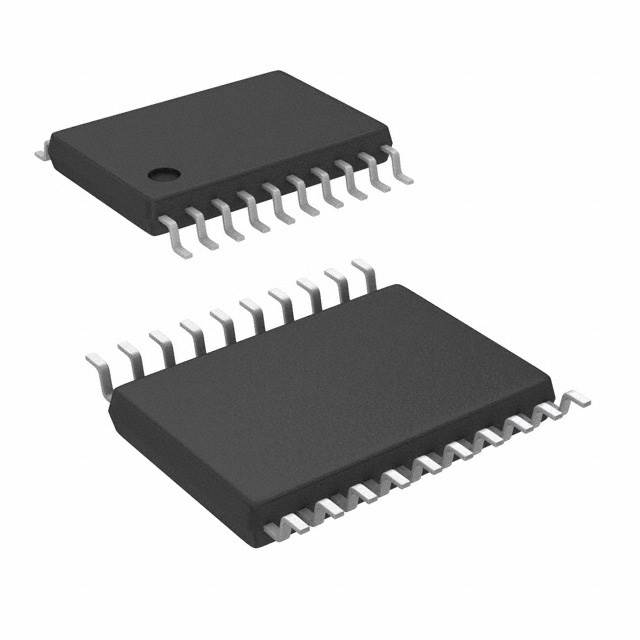
20-Lead TSSOP
6.5mm x 4.4mm x 0.925mm
package body
G Package
Top View
The Preliminary Information presented herein represents a product in pre-production. The noted characteristics are based on initial product characterization and/or qualification.
Integrated Device Technology, Incorporated (IDT) reserves the right to change any circuitry or specifications without notice.
IDT™ / ICS™ LVDS CLOCK MULTIPLIER
1
ICS874S336AG OCTOBER 17, 2007
�ICS874S336
LVDS CLOCK MULTIPLIER
PRELIMINARY
Block Diagram
BYPASS
CLK_SEL
CLK
1
nCLK
1
/P
0
SE_CLK
PLL
Q
/N
nQ
0
/M
FB_IN
QFB
nQFB
nFB_IN
S_CLOCK
S_DATA
S_LOAD
CONFIGURATION
INTERFACE
LOGIC
IDT™ / ICS™ LVDS CLOCK MULTIPLIER
2
ICS874S336AG OCTOBER 17, 2007
�ICS874S336
LVDS CLOCK MULTIPLIER
PRELIMINARY
Functional Description
The ICS874S336 features a fully integrated PLL and therefore
requires no external components for setting the loop bandwidth.
The VCO of the PLL operates over a range of 1.2GHz to 2GHz.
The output of the M divider is also applied to the phase detector.
frequencies are found in Table 3B, Programmable VCO Frequency
Function Table. The actual data bits can be found in Tables 3C, 3D
and 3E.
Serial operation occurs when S_LOAD is LOW. The shift register
is loaded by sampling the S_DATA bits with the rising edge of
S_CLOCK. The contents of the shift register are loaded into the M,
N and P dividers when S_LOAD transitions from LOW-to-HIGH.
The divide values are latched on the HIGH-to-LOW transition of
S_LOAD. If S_LOAD is held HIGH, data at the S_DATA input is
passed directly to the dividers on each rising edge of S_CLOCK.
The serial mode can be used to program the M, N and P bits.
The phase detector and the M divider force the VCO output
frequency to be M times the reference frequency by adjusting the
VCO control voltage. Note that for some values of M (either too
high or too low), the PLL will not achieve lock. The output of the
VCO is scaled by a divider prior to being sent to each of the
LVPECL output buffers. The divider provides a 50% output duty
cycle.
The relationship between the VCO frequency, the input frequency
and the M divider is defined as follows:
fIN x M x N
fVCO = ----------------------------- x 2
P
The M, N, and P values used to obtain the proper video
SERIAL LOADING
S_CLOCK
S_DATA
P1
t
S_LOAD
S
t
P0
N6
N5
N4
N3
N2
N1
N0
M4
M3
M2
M1
M0
H
t
S
Figure 1. Serial Load Operation
IDT™ / ICS™ LVDS CLOCK MULTIPLIER
3
ICS874S336AG OCTOBER 17, 2007
�ICS874S336
LVDS CLOCK MULTIPLIER
PRELIMINARY
Table 1. Pin Descriptions
Number
Name
Type
1, 4, 8
VDD
Power
2, 3
Q, nQ
Output
Description
Core supply pins.
Differential output pair. LVDS interface levels.
5
S_LOAD
Input
Pulldown
Controls transition of data from shift register into the dividers.
LVCMOS/LVTTL interface levels.
6
S_DATA
Input
Pulldown
Shift register serial input. Data sampled on the rising edge of S_CLOCK.
LVCMOS/LVTTL interface levels.
7
S_CLOCK
Input
Pulldown
Clocks in serial data present at S_DATA input into the shift register on the
rising edge of S_CLOCK. LVCMOS/LVTTL interface levels.
9
CLK
Input
Pulldown
Non-inverting differential clock input.
Pullup/Pulldown
Inverting differential clock input. VDD/2 default when left floating.
10
nCLK
Input
11, 20
GND
Power
12
CLK_SEL
Input
Pullup
13
SE_CLK
Input
Pulldown
Single-ended clock input. LVCMOS/LVTTL interface levels.
14
BYPASS
Input
Pulldown
Selects between the PLL and reference clock as the input to the
dividers.When LOW, selects PLL. When HIGH, selects reference clock.
LVCMOS/LVTTL interface levels.
15
FB_IN
Input
Pulldown
Non-inverting differential clock input.
16
nFB_IN
Input
Pullup/Pulldown
17
VDDA
Power
Analog supply pin.
18, 19
QFB, nQFB
Output
Differential output pair. LVDS interface levels.
Negative supply pin.
Selects the reference clock. When LOW selects SE_CLK as the clock
source. When HIGH selects CLK, nCLK as the clock source.
LVCMOS/LVTTL interface levels.
Inverting differential clock input. VDD/2 default when left floating.
NOTE: Pullup and Pulldown refer to internal input resistors. See Table 2, Pin Characteristics, for typical values.
Table 2. Pin Characteristics
Symbol
Parameter
CIN
Input Capacitance
4
pF
RPULLUP
Input Pullup Resistor
51
kΩ
RPULLDOWN
Input Pulldown Resistor
51
kΩ
IDT™ / ICS™ LVDS CLOCK MULTIPLIER
Test Conditions
4
Minimum
Typical
Maximum
Units
ICS874S336AG OCTOBER 17, 2007
�ICS874S336
LVDS CLOCK MULTIPLIER
PRELIMINARY
Function Tables
Table 3A. Parallel and Serial Mode Function Table
Inputs
S_LOAD
S_CLOCK
S_DATA
Conditions
L
X
X
L
↑
Data
Shift register is loaded with data on S_DATA on each rising edge of S_CLOCK.
↑
L
Data
Contents of the shift register are passed to the M, N and P dividers.
↓
L
Data
M, N and P divider values are latched.
L
X
X
Serial input do not affect shift registers.
H
↑
Data
Data is latched into input registers and remains loaded until next LOW transition or until a
serial event occurs.
S_DATA passed directly to M, N and P dividers as it is clocked.
NOTE: L = LOW
H = HIGH
X = Don’t care
↑ = Rising edge transition
↓ = Falling edge transition
Table 3B. Device Configuration Table
Input Frequency (MHz)
P Divide Value
N Divide Value
Min
Max
14
17
1
10
14
17
1
14
17
14
M Divide Value
Output Frequency (MHz)
Min
Max
12
168
204
10
10
140
170
2
12
17
119
144.5
17
4
14
28
98
119
14
17
4
16
24
84
102
14
17
4
20
20
70
85
14
17
4
22
17
59.5
72.25
14
17
4
28
14
49
59.5
14
17
4
32
12
42
51
14
17
8
38
20
35
42.5
14
17
8
46
17
29.75
36.125
14
17
8
56
14
24.5
29.75
14
17
8
64
12
21
25.5
14
17
8
80
10
17.5
21.25
14
17
8
100
8
14
17
14
17
8
110
7
12.25
14.875
14
17
8
130
6
10.5
12.75
14
17
8
160
5
8.75
10.6
IDT™ / ICS™ LVDS CLOCK MULTIPLIER
5
ICS874S336AG OCTOBER 17, 2007
�ICS874S336
LVDS CLOCK MULTIPLIER
PRELIMINARY
Table 3C. Pre-Divider (P) Configuration Table
P Divide
P1
P0
1
0
0
2
0
1
4
1
0
8
1
1
Table 3D. Output Divider (N) Configuration Table
N Divide
N6
N5
N4
N3
N2
N1
N0
10
0
0
0
0
1
0
1
12
0
0
0
0
1
1
0
14
0
0
0
0
1
1
1
16
0
0
0
1
0
0
0
20
0
0
0
1
0
1
0
22
0
0
0
1
0
1
1
28
0
0
0
1
1
1
0
32
0
0
1
0
0
0
0
38
0
0
1
0
0
1
1
46
0
0
1
0
1
1
1
56
0
0
1
1
1
0
0
64
0
1
0
0
0
0
0
80
0
1
0
1
0
0
0
100
0
1
1
0
0
1
0
110
0
1
1
0
1
1
1
130
1
0
0
0
0
0
1
160
1
0
1
0
0
0
0
IDT™ / ICS™ LVDS CLOCK MULTIPLIER
6
ICS874S336AG OCTOBER 17, 2007
�ICS874S336
LVDS CLOCK MULTIPLIER
PRELIMINARY
Table 3E. Feedback Divider (M) Configuration Table
M Divide
M4
M3
M2
M1
M0
5
0
0
1
0
1
6
0
0
1
1
0
7
0
0
1
1
1
8
0
1
0
0
0
10
0
1
0
1
0
12
0
1
1
0
0
14
0
1
1
1
0
17
1
0
0
0
1
20
1
0
1
0
0
24
1
1
0
0
0
28
1
1
1
0
0
IDT™ / ICS™ LVDS CLOCK MULTIPLIER
7
ICS874S336AG OCTOBER 17, 2007
�ICS874S336
LVDS CLOCK MULTIPLIER
PRELIMINARY
Absolute Maximum Ratings
NOTE: Stresses beyond those listed under Absolute Maximum Ratings may cause permanent damage to the device.
These ratings are stress specifications only. Functional operation of product at these conditions or any conditions beyond
those listed in the DC Characteristics or AC Characteristics is not implied. Exposure to absolute maximum rating conditions for
extended periods may affect product reliability.
Item
Rating
Supply Voltage, VDD
4.6V
Inputs, VI
-0.5V to VDD + 0.5V
Outputs, IO (LVDS)
Continuos Current
Surge Current
10mA
15mA
Outputs, IO (LVDS)
Continuos Current
Surge Current
50mA
100mA
Package Thermal Impedance, θJA
87.2°C/W (0 mps)
Storage Temperature, TSTG
-65°C to 150°C
DC Electrical Characteristics
Table 4A. LVDS Power Supply DC Characteristics,VDD = 3.3V ± 5%, TA = 0°C to 70°C
Symbol
Parameter
VDD
Test Conditions
Minimum
Typical
Maximum
Units
Positive Supply Voltage
3.135
3.3
3.465
V
VDDA
Analog Supply Voltage
VDD – 0.15
3.3
VDD
V
IDD
Power Supply Current
115
mA
IDDA
Analog Supply Current
15
mA
Table 4B. LVCMOS/LVTTL DC Characteristics, VDD = 3.3V ± 5%, TA = 0°C to 70°C
Symbol
Parameter
VIH
Input High Voltage
VIL
Input Low Voltage
IIH
IIL
Input High Current
Input Low Current
Test Conditions
Minimum
Typical
Maximum
Units
2
VDD + 0.3
V
-0.3
0.8
V
SE_CLK, BYPASS,
S_CLOCK, S_DATA,
S_LOAD
VDD = VIN = 3.465V
150
µA
CLK_SEL
VDD = VIN = 3.465V
5
µA
SE_CLK, BYPASS,
S_CLOCK, S_DATA,
S_LOAD
VDD = 3.465V, VIN = 0V
-5
µA
CLK_SEL
VDD = 3.465V, VIN = 0V
-150
µA
IDT™ / ICS™ LVDS CLOCK MULTIPLIER
8
ICS874S336AG OCTOBER 17, 2007
�ICS874S336
LVDS CLOCK MULTIPLIER
PRELIMINARY
Table 4C. Differential DC Characteristics, VDD = 3.3V ± 5%, TA = 0°C to 70°C
Symbol
Parameter
IIH
Input High Current
IIL
Test Conditions
CLK/nCLK,
FB_IN/nFB_IN
Minimum
Typical
VDD = VIN = 3.465V
Maximum
Units
150
µA
CLK, FB_IN
VDD = 3.465V,
VIN = 0V
-5
µA
nCLK, nFB_IN
VDD = 3.465V,
VIN = 0V
-150
µA
Input Low Current
VPP
Peak-to-Peak Voltage; NOTE 1
VCMR
Common Mode Input Voltage; NOTE 1, 2
0.15
1.3
V
GND + 0.5
VDD – 0.85
V
NOTE 1: VIL should not be less than -0.3V.
NOTE 2: Common mode input voltage is defined as VIH.
Table 4D. LVDS DC Characteristics, VDD = 3.3V ± 5%, TA = 0°C to 70°C
Symbol
Parameter
Test Conditions
Minimum
Typical
Maximum
Units
VOD
Differential Output Voltage
370
mV
∆VOD
VOD Magnitude Change
50
mV
VOS
Offset Voltage
1.22
V
∆VOS
VOS Magnitude Change
50
mV
Table 5. Input Frequency Characteristics, VDD = 3.3V ± 5%, TA = 0°C to 70°C
Symbol
Parameter
fIN
Input
Frequency
Test Conditions
CLK/nCLK,
SE_CLK; NOTE 1
Minimum
Typical
14
S_CLOCK
Maximum
Units
17
MHz
10
MHz
NOTE 1: For the CLK/nCLK and SE_CLK frequency range, the M value must be set for the VCO to operate within the TBD MHz to TBD
MHz range.
Table 6. AC Characteristics, VDD = 3.3V ± 5%, TA = 0°C to 70°C
Parameter Symbol
fMAX
Output Frequency
tjit(cc)
Cycle-to-Cycle Jitter; NOTE 1
t(Ø)
tjit(per)
tR / tF
Output Rise/Fall Time
odc
Output Duty Cycle
Test Conditions
Minimum
Typical
8.75
Maximum
Units
204
MHz
TBD
ps
Static Phase Offset; NOTE 1
TBD
ps
Period Jitter, RMS; NOTE 1
TBD
ps
270
ps
50
%
20% to 80%
NOTE 1: This parameter is defined in accordance with JEDEC Standard 65.
IDT™ / ICS™ LVDS CLOCK MULTIPLIER
9
ICS874S336AG OCTOBER 17, 2007
�ICS874S336
LVDS CLOCK MULTIPLIER
PRELIMINARY
Parameter Measurement Information
VDD
SCOPE
3.3V±5%
POWER SUPPLY
+ Float GND –
nCLK
Qx
VDD
V
V
Cross Points
PP
VDDA
CMR
CLK
LVDS
nQx
GND
3.3V LVDS Output Load AC Test Circuit
Differential Input Level
VOH
nQ, nQFB
VREF
Q, QFB
➤
1σ contains 68.26% of all measurements
2σ contains 95.4% of all measurements
3σ contains 99.73% of all measurements
4σ contains 99.99366% of all measurements
6σ contains (100-1.973x10⁻⁷)% of all measurements
➤
VOL
➤
tcycle n
tcycle n+1
➤
tjit(cc) = tcycle n – tcycle n+1
1000 Cycles
Histogram
Reference Point
Mean Period
(Trigger Edge)
(First edge after trigger)
Period Jitter, RMS
Cycle-to-Cycle Jitter
nQ, nQFB
Q, QFB
80%
80%
t PW
t
VOD
Clock
Outputs
20%
20%
tR
tF
odc =
PERIOD
t PW
x 100%
t PERIOD
Output Duty Cycle/Pulse Width/Period
Output Rise/Fall Time
IDT™ / ICS™ LVDS CLOCK MULTIPLIER
10
ICS874S336AG OCTOBER 17, 2007
�ICS874S336
LVDS CLOCK MULTIPLIER
PRELIMINARY
Parameter Measurement Information, continued
VDD
VDD
out
LVDS
➤
out
➤
out
DC Input
➤
LVDS
100
➤
VOD/∆ VOD
VOS/∆ VOS
out
➤
DC Input
➤
Offset Voltage Setup
Differential Output Voltage Setup
Application Information
Wiring the Differential Input to Accept Single-Ended Levels
Figure 2 shows how the differential input can be wired to accept
single-ended levels. The reference voltage V_REF = VDD/2 is
generated by the bias resistors R1, R2 and C1. This bias circuit
should be located as close as possible to the input pin. The ratio of
R1 and R2 might need to be adjusted to position the V_REF in the
center of the input voltage swing. For example, if the input clock
swing is only 2.5V and VDD = 3.3V, V_REF should be 1.25V and
R2/R1 = 0.609.
VDD
R1
1K
Single Ended Clock Input
CLK
V_REF
nCLK
C1
0.1u
R2
1K
Figure 2. Single-Ended Signal Driving Differential Input
IDT™ / ICS™ LVDS CLOCK MULTIPLIER
11
ICS874S336AG OCTOBER 17, 2007
�ICS874S336
LVDS CLOCK MULTIPLIER
PRELIMINARY
Differential Clock Input Interface
The CLK /nCLK accepts LVDS, LVPECL, LVHSTL, SSTL, HCSL
and other differential signals. Both VSWING and VOH must meet the
VPP and VCMR input requirements. Figures 3A to 3F show interface
examples for the HiPerClockS CLK/nCLK input driven by the most
common driver types. The input interfaces suggested here are
examples only. Please consult with the vendor of the driver
component to confirm the driver termination requirements. For
example, in Figure 3A, the input termination applies for IDT
HiPerClockS open emitter LVHSTL drivers. If you are using an
LVHSTL driver from another vendor, use their termination
recommendation.
3.3V
3.3V
3.3V
1.8V
Zo = 50Ω
Zo = 50Ω
CLK
CLK
Zo = 50Ω
nCLK
Zo = 50Ω
nCLK
HiPerClockS
Input
LVHSTL
R1
50
IDT
HiPerClockS
LVHSTL Driver
HiPerClockS
Input
LVPECL
R2
50
R1
50
R2
50
R2
50
Figure 3A. HiPerClockS CLK/nCLK Input
Driven by an IDT Open Emitter
HiPerClockS LVHSTL Driver
Figure 3B. HiPerClockS CLK/nCLK Input
Driven by a 3.3V LVPECL Driver
3.3V
3.3V
3.3V
R3
125
3.3V
R4
125
3.3V
Zo = 50Ω
Zo = 50Ω
CLK
CLK
R1
100
Zo = 50Ω
nCLK
HiPerClockS
Input
LVPECL
R1
84
R2
84
Figure 3C. HiPerClockS CLK/nCLK Input
Driven by a 3.3V LVPECL Driver
2.5V
nCLK
Zo = 50Ω
Receiver
LVDS
Figure 3D. HiPerClockS CLK/nCLK Input
Driven by a 3.3V LVDS Driver
2.5V
3.3V
3.3V
2.5V
*R3
33
R3
120
Zo = 50Ω
R4
120
Zo = 60Ω
CLK
CLK
Zo = 50Ω
Zo = 60Ω
nCLK
nCLK
HCSL
*R4
33
R1
50
R2
50
HiPerClockS
Input
HiPerClockS
SSTL
R1
120
R2
120
*Optional – R3 and R4 can be 0Ω
Figure 3F. HiPerClockS CLK/nCLK Input
Driven by a 2.5V SSTL Driver
Figure 3E. HiPerClockS CLK/nCLK Input
Driven by a 3.3V HCSL Driver
IDT™ / ICS™ LVDS CLOCK MULTIPLIER
12
ICS874S336AG OCTOBER 17, 2007
�ICS874S336
LVDS CLOCK MULTIPLIER
PRELIMINARY
Power Supply Filtering Technique
As in any high speed analog circuitry, the power supply pins are
vulnerable to random noise. The ICS874S336 provides separate
power supplies to isolate any high switching noise from the outputs
to the internal PLL. VDD and VDDA should be individually
connected to the power supply plane through vias, and bypass
capacitors should be used for each pin. To achieve optimum jitter
performance, power supply isolation is required. Figure 4
illustrates how a 10Ω resistor along with a 10µF and a 0.01µF
bypass capacitor should be connected to each VDDA pin.
3.3V
VDD
.01µF
10Ω
.01µF
10µF
VDDA
Figure 4. Power Supply Filtering
Recommendations for Unused Input and Output Pins
Inputs:
Outputs:
CLK/nCLK Inputs
LVDS Outputs
For applications not requiring the use of the differential input, both
CLK and nCLK can be left floating. Though not required, but for
additional protection, a 1kΩ resistor can be tied from CLK to
ground.
All unused LVDS output pairs can be either left floating or
terminated with 100Ω across. If they are left floating, there should
be no trace attached.
SE_CLK Input
For applications not requiring the use of a clock input, it can be left
floating. Though not required, but for additional protection, a 1kΩ
resistor can be tied from the SE_CLK input to ground.
LVCMOS Control Pins
All control pins have internal pull-ups or pull-downs; additional
resistance is not required but can be added for additional
protection. A 1kΩ resistor can be used.
3.3V LVDS Driver Termination
A general LVDS interface is shown in Figure 5. In a 100Ω
differential transmission line environment, LVDS drivers require a
matched load termination of 100Ω across near the receiver input.
For a multiple LVDS outputs buffer, if only partial outputs are used,
it is recommended to terminate the unused outputs.
3.3V
50Ω
3.3V
LVDS Driver
+
R1
100Ω
–
50Ω
100Ω Differential Transmission Line
Figure 5. Typical LVDS Driver Termination
IDT™ / ICS™ LVDS CLOCK MULTIPLIER
13
ICS874S336AG OCTOBER 17, 2007
�ICS874S336
LVDS CLOCK MULTIPLIER
PRELIMINARY
Schematic Example
Figure 6 shows an example of ICS874S336 application schematic.
In this example, the device is operated at VDD = 3.3V. The
decoupling capacitors should be located as close as possible to
the power pin. Two examples of LVDS terminations are shown in
this schematic. The input is driven either by a 3.3V LVPECL driver
or a 3.3V LVCMOS. .
Figure 6. ICS874S336 Schematic Example
IDT™ / ICS™ LVDS CLOCK MULTIPLIER
14
ICS874S336AG OCTOBER 17, 2007
�ICS874S336
LVDS CLOCK MULTIPLIER
PRELIMINARY
Power Considerations
This section provides information on power dissipation and junction temperature for the ICS874S336.
Equations and example calculations are also provided.
1.
Power Dissipation.
The total power dissipation for the ICS74S336 is the sum of the core power plus the power dissipated in the load(s).
The following is the power dissipation for VDD = 3.3V + 5% = 3.465V, which gives worst case results.
•
Power (core)MAX = VDD_MAX * (IDD_MAX + IDDA_MAX) = 3.465V * (115mA + 15mA) = 450.45mW
2. Junction Temperature.
Junction temperature, Tj, is the temperature at the junction of the bond wire and bond pad and directly affects the reliability of the device.
The maximum recommended junction temperature for HiPerClockS devices is 125°C.
The equation for Tj is as follows: Tj = θJA * Pd_total + TA
Tj = Junction Temperature
θJA = Junction-to-Ambient Thermal Resistance
Pd_total = Total Device Power Dissipation (example calculation is in section 1 above)
TA = Ambient Temperature
In order to calculate junction temperature, the appropriate junction-to-ambient thermal resistance θJA must be used. Assuming no air flow
and a multi-layer board, the appropriate value is 87.2°C/W per Table 7 below.
Therefore, Tj for an ambient temperature of 70°C with all outputs switching is:
70°C + 0.450W * 87.2°C/W = 109.2°C. This is well below the limit of 125°C.
This calculation is only an example. Tj will obviously vary depending on the number of loaded outputs, supply voltage, air flow and the type
of board (single layer or multi-layer).
Table 7. Thermal Resistance θJA for 20 Lead TSSOP, Forced Convection
θJA by Velocity
Meters per Second
Multi-Layer PCB, JEDEC Standard Test Boards
IDT™ / ICS™ LVDS CLOCK MULTIPLIER
0
1
2.5
87.2°C/W
82.9°C/W
80.7°C/W
15
ICS874S336AG OCTOBER 17, 2007
�ICS874S336
LVDS CLOCK MULTIPLIER
PRELIMINARY
Reliability Information
Table 8. θJA vs. Air Flow Table for a 20 Lead TSSOP
θJA by Velocity
Meters per Second
Multi-Layer PCB, JEDEC Standard Test Boards
0
1
2.5
87.2°C/W
82.9°C/W
80.7°C/W
Transistor Count
The transistor count for ICS874S336 is: 2434
Package Outline and Package Dimension
Package Outline - G Suffix for 20 Lead TSSOP
Table 9. Package Dimensions
All Dimensions in Millimeters
Symbol
Minimum
Maximum
N
20
A
1.20
A1
0.05
0.15
A2
0.80
1.05
b
0.19
0.30
c
0.09
0.20
D
6.40
6.60
E
6.40 Basic
E1
4.30
4.50
e
0.65 Basic
L
0.45
0.75
α
0°
8°
aaa
0.10
Reference Document: JEDEC Publication 95, MO-153
IDT™ / ICS™ LVDS CLOCK MULTIPLIER
16
ICS874S336AG OCTOBER 17, 2007
�ICS874S336
LVDS CLOCK MULTIPLIER
PRELIMINARY
Ordering Information
Table 9. Ordering Information
Part/Order Number
874S336AG
874S336AGT
874S336AGLF
874S336AGLFT
Marking
TBD
TBD
ICS874S336AL
ICS874S336AL
Package
20 Lead TSSOP
20 Lead TSSOP
“Lead-Free” 20 Lead TSSOP
“Lead-Free” 20 Lead TSSOP
Shipping Packaging
Tube
2500 Tape & Reel
Tube
2500 Tape & Reel
Temperature
0°C to 70°C
0°C to 70°C
0°C to 70°C
0°C to 70°C
NOTE: Parts that are ordered with an "LF" suffix to the part number are the Pb-Free configuration and are RoHS compliant.
While the information presented herein has been checked for both accuracy and reliability, Integrated Device Technology (IDT) assumes no responsibility for either its use or for
the infringement of any patents or other rights of third parties, which would result from its use. No other circuits, patents, or licenses are implied. This product is intended for use
in normal commercial applications. Any other applications, such as those requiring extended temperature ranges, high reliability or other extraordinary environmental requirements
are not recommended without additional processing by IDT. IDT reserves the right to change any circuitry or specifications without notice. IDT does not authorize or warrant any
IDT product for use in life support devices or critical medical instruments.
IDT™ / ICS™ LVDS CLOCK MULTIPLIER
17
ICS874S336AG OCTOBER 17, 2007
�ICS874S336
LVDS CLOCK MULTIPLIER
PRELIMINARY
Innovate with IDT and accelerate your future networks. Contact:
www.IDT.com
www.IDT.com
For Sales
For Tech Support
800-345-7015
408-284-8200
Fax: 408-284-2775
netcom@idt.com
480-763-2056
Corporate Headquarters
Asia Pacific and Japan
Europe
Integrated Device Technology, Inc.
6024 Silver Creek Valley Road
San Jose, CA 95138
United States
800 345 7015
+408 284 8200 (outside U.S.)
Integrated Device Technology
Singapore (1997) Pte. Ltd.
Reg. No. 199707558G
435 Orchard Road
#20-03 Wisma Atria
Singapore 238877
+65 6 887 5505
IDT Europe, Limited
321 Kingston Road
Leatherhead, Surrey
KT22 7TU
England
+44 (0) 1372 363 339
Fax: +44 (0) 1372 378851
© 2007 Integrated Device Technology, Inc. All rights reserved. Product specifications subject to change without notice. IDT and the IDT logo are trademarks of Integrated Device
Technology, Inc. Accelerated Thinking is a service mark of Integrated Device Technology, Inc. All other brands, product names and marks are or may be trademarks or registered
trademarks used to identify products or services of their respective owners.
Printed in USA
�