87974I
Low Skew, 1-to-15,
LVCMOS/LVTTL Clock Generator
GENERAL DESCRIPTION
FEATURES
The 87974I is a low skew, low jitter 1-to-15 LVCMOS/
LVTTL Clock Generator/Zero Delay Buffer. The device
has a fully integrated PLL and three banks whose divider
ratios can be independently controlled, providing output
frequency relationships of 1:1, 2:1, 3:1, 3:2, 3:2:1. In
addition, the external feedback connection provides for a wide
selection of output-to-input frequency ratios. The CLK0 and
CLK1 pins allow for redundant clocking on the input and dynamically switching the PLL between two clock sources.
• Fully integrated PLL
Data Sheet
• Fifteen single ended 3.3V LVCMOS/LVTTL outputs
• Two LVCMOS/LVTTL clock inputs for redundant clock applications
• CLK0 and CLK1 accepts the following input levels:
LVCMOS/LVTTL
• Output frequency range: 8.33MHz to 125MHz
• VCO range: 200MHz to 500MHz
Guaranteed low jitter and output skew characteristics make
the 87974I ideal for those applications demanding well defined
performance and repeatability.
• External feedback for ”zero delay” clock regeneration
• Cycle-to-cycle jitter: ±100ps (typical)
• Output skew: 350ps (maximum)
• 3.3V operating supply
• -40°C to 85°C ambient operating temperature
• Available in lead-free RoHS-compliant package
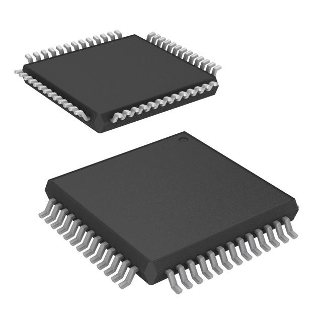
PIN ASSIGNMENT
52-Lead LQFP
10mm x 10mm x 1.4mm package body
Y package
Top View
©2016 Integrated Device Technology, Inc
1
Revision E January 26, 2016
�87974I Data Sheet
BLOCK DIAGRAM
©2016 Integrated Device Technology, Inc
2
Revision E January 26, 2016
�87974I Data Sheet
SIMPLIFIED BLOCK DIAGRAM
CLK_EN
SEL_A
VCO_SEL
0
CLK_SEL
CLK0
CLK1
1
0
÷2
0
÷4
1
SEL_A
0
÷2
1
÷4
D Q
SEL_B
0
÷2
1
÷4
D Q
SEL_C
0
÷4
1
÷6
D Q
5
QA0:QA4
PLL
1
FB_IN
PLL_SEL
5
QB0:QB4
SEL_B
4
QC0:QC3
SEL_C
FB_0 FB_1
0
0 ÷4
0
1 ÷6
1
0 ÷8
1
1 ÷12
D Q
QFB
FB_SEL(0:1)
2
nMR/OE
©2016 Integrated Device Technology, Inc
3
Revision E January 26, 2016
�87974I Data Sheet
TABLE 1. PIN DESCRIPTIONS
Number
Name
1, 15, 19,
24, 30, 35, 39,
43, 47, 51
GND
Type
Power
Description
Power supply ground.
Active HIGH outputs enabled (active). When LOW, outputs are disabled
(High-impedance state) and reset of the device. During reset/output
disable the PLL feedback loop is open and the internal VCO is tied to its
lowest frequency. The 87974I requires reset after any loss of PLL lock.
Loss of PLL lock may occur when the external feedback path is interrupted. The length of the reset pulse should be greater than one reference
clock cycle (CLKx)
Synchronizing clock enable. When HIGH, clock outputs QAx:QCx
are enabled. When LOW, clock outputs QAx:QCx are low.
LVCMOS / LVTTL interface levels.
Selects divide value for Bank B output as described in Table 3D. LVCMOS
/ LVTTL interface levels.
Selects divide value for Bank C output as described in Table 3D. LVCMOS
/ LVTTL interface levels.
Selects between the PLL and the reference clock as the input to the dividers. When HIGH, selects PLL. When LOW, selects the reference clock.
LVCMOS / LVTTL interface levels.
Selects divide value for Bank A output as described in Table 3D. LVCMOS
/ LVTTL interface levels.
Clock select input. When HIGH, selects CLK1. When LOW,
selects CLK0. LVCMOS / LVTTL interface levels.
2
nMR/OE
Input
Pullup
3
CLK_EN
Input
Pullup
4
SEL_B
Input
Pulldown
5
SEL_C
Input
Pulldown
6
PLL_SEL
Input
Pullup
7
SEL_A
Input
Pulldown
8
CLK_SEL
Input
Pulldown
9
CLK0
Input
Pulldown Reference clock input. LVCMOS / LVTTL interface levels.
10
CLK1
Input
11, 27, 42
nc
Unused
12
VDD
Power
Core supply pin.
13
VDDA
Power
Analog supply pin.
Pullup
Reference clock input. LVCMOS / LVTTL interface levels.
No connect.
16, 18,
21, 23, 25
FB_SEL0, FB_
SEL1
QA4, QA3,
QA2, QA1, QA0
17, 22, 26
VDDOA
Power
Output supply pins for Bank A clock outputs.
28
VDDOFB
Power
Output supply pin for QFB clock output.
29
QFB
Output
14, 20
Input
Pulldown
Output
Selects divide value for Bank feedback output as described in
Table 3E. LVCMOS / LVTTL interface levels.
Bank A clock outputs. 7Ω typical output impedance.
LVCMOS / LVTTL interface levels.
Clock output. LVCMOS / LVTTL interface levels.
Pullup
Feedback input to phase detector for generating clocks with
“zero delay”. Connect to pin 29.
LVCMOS / LVTTL interface levels.
Bank B clock outputs. 7Ω typical output impedance.
LVCMOS / LVTTL interface levels.
31
FB_IN
Input
32, 34,
36, 38, 40
QB4, QB3,
QB2, QB1, QB0
Output
33, 37, 41
VDDOB
Power
Output supply pins for Bank B clock outputs.
44, 46,
48, 50
QC3, QC2, QC1,
QC0
Output
Bank C clock outputs. 7Ω typical output impedance.
LVCMOS / LVTTL interface levels.
45, 49
VDDOC
Power
Output supply pins for Bank C clock outputs.
52
VCO_SEL
Input
Pulldown
Selects VCO ÷ 4 when HIGH. Selects VCO ÷ 2 when LOW.
LVCMOS / LVTTL interface levels.
NOTE: and refer to internal input resistors. See Table 2, Pin Characteristics, for typical values.
Pullup
Pulldown
©2016 Integrated Device Technology, Inc
4
Revision E January 26, 2016
�87974I Data Sheet
TABLE 2. PIN CHARACTERISTICS
Symbol
Parameter
Test Conditions
Minimum
Typical
Maximum
Units
CIN
Input Capacitance
4
pF
RPULLUP
Input Pullup Resistor
51
KΩ
RPULLDOWN
51
KΩ
CPD
Input Pulldown Resistor
Power Dissipation Capacitance
(per output); Note 1
ROUT
Output Impedance
VDD, VDDA, VDDOx = 3.465V
5
7
15
pF
12
Ω
NOTE 1: VDDOx denotes VDDOA, VDDOB, VDDOC, VDDOFB.
TABLE 3A. OUTPUT CONTROL PIN FUNCTION TABLE
Inputs
Outputs
nMR/OE
CLK_EN
QA0:QA4
QB0:QB4
QC0:QC3
QFB
0
X
HiZ
HiZ
HiZ
HiZ
1
0
LOW
LOW
LOW
Enable
1
1
Enable
Enable
Enable
Enable
TABLE 3B. OPERATING MODE FUNCTION TABLE
Inputs
TABLE 3C. PLL INPUT FUNCTION TABLE
Inputs
Operating Mode
PLL_SEL
CLK_SEL
PLL Input
0
Bypass
0
CLK0
1
PLL
1
CLK1
TABLE 3D. SELECT PIN FUNCTION TABLE
SEL_A
QAx
SEL_B
QBx
SEL_C
QCx
0
÷2
0
÷2
0
÷4
1
÷4
1
÷4
1
÷6
TABLE 3E. FB SELECT FUNCTION TABLE
Inputs
TABLE 3F. VCO SELECT FUNCTION TABLE
Inputs
Outputs
FB_SEL1
FB_SEL0
QFB
VCO_SEL
0
0
÷4
0
VCO/2
1
0
÷6
1
VCO/4
0
1
÷8
1
1
÷ 12
©2016 Integrated Device Technology, Inc
5
fVCO
Revision E January 26, 2016
�87974I Data Sheet
ABSOLUTE MAXIMUM RATINGS
Supply Voltage, VDD
4.6V
Inputs, VI
-0.5V to VDD + 0.5 V
Outputs, VO
-0.5V to VDDO + 0.5V
Package Thermal Impedance, θJA
73.2°C/W (0 lfpm)
Storage Temperature, TSTG
-65°C to 150°C
NOTE: Stresses beyond those listed under Absolute
Maximum Ratings may cause permanent damage to the
device. These ratings are stress specifications only. Functional
operation of product at these conditions or any conditions
beyond those listed in the DC Characteristics or AC Characteristics is not implied. Exposure to absolute maximum rating
conditions for extended periods may affect product reliability.
TABLE 4A. POWER SUPPLY DC CHARACTERISTICS, VDD = VDDA = VDDO = 3.3V±5%, TA = -40°C TO 85°C
X
Symbol
Parameter
VDD
VDDA
Test Conditions
Minimum
Typical
Maximum
Units
Core Supply Voltage
3.135
3.3
3.465
V
Analog Supply Voltage
2.935
3.3
3.465
V
VDDOx
Output Supply Voltage; NOTE 1
3.135
3.3
3.465
V
IDD
Power Supply Current
121
mA
IDDA
Analog Supply Current
15
mA
IDDOx
Output Supply Current; NOTE 2
24
mA
NOTE 1: VDDOx denotes VDDOA, VDDOB, VDDOC, VDDOFB.
NOTE 2: IDDOx denotes IDDOA, IDDOB, IDDOC, IDDOFB
TABLE 4B. LVCMOS/LVTTL DC CHARACTERISTICS, VDD = VDDA = VDDO = 3.3V±5%, TA = -40°C TO 85°C
X
Symbol
VIH
VIL
IIH
IIL
Parameter
Input
High Voltage
Input
Low Voltage
Input
High Current
Input
Low Current
Test Conditions
Minimum
Typical
Maximum
Units
SEL_A:SEL_C, nMR/OE,
VCO_SEL, PLL_SEL,
CLK_SEL, CLK_EN,
FB_SEL0, FB_SEL1, FB_IN
2
VDD
V
CLK0, CLK1
2
VDD
V
SEL_A:SEL_C, nMR/OE,
VCO_SEL, PLL_SEL,
CLK_SEL, CLK_EN,
FB_SEL0, FB_SEL1, FB_IN
0.8
V
CLK0, CLK1
0.8
V
100
µA
5
µA
FB_SEL0, FB_SEL1,
SEL_A:SEL_C, CLK0, VCO_
VDD = VIN = 3.465V
SEL, CLK_SEL
CLK1, FB_IN, nMR/OE, PLL_
VDD = VIN = 3.465V
SEL, CLK_EN
FB_SEL0, FB_SEL1,
SEL_A:SEL_C, CLK0, VCO_ VIN = 0V, VDD = 3.465V
SEL, CLK_SEL
CLK1, FB_IN, nMR/OE, PLL_
VIN = 0V, VDD = 3.465V
SEL, CLK_EN
VOH
Output High Voltage; NOTE 1
VOL
Output Low Voltage; NOTE 1
-5
µA
-100
µA
2.4
V
0.5
V
NOTE 1: Outputs terminated with 50Ω to VDDOx/2.
©2016 Integrated Device Technology, Inc
6
Revision E January 26, 2016
�87974I Data Sheet
TABLE 5. AC CHARACTERISTICS, VDD = VDDA = VDDO = 3.3V±5%, TA = -40°C TO 85°C
X
Symbol
Parameter
Test Conditions
Maximum
Units
Qx ¸ ÷2, VCO ¸ ÷2
Minimum
Typical
125
MHz
Qx ¸ ÷4, VCO ¸ ÷2
63
MHz
fMAX
Output Frequency
fVCO
PLL VCO Lock Range; NOTE 5
tPD
SYNC to Feedback
Propagation Delay; NOTE 2, 5
tsk(o)
Output Skew; NOTE 4, 5
tjit(cc)
Cycle-to-Cycle Jitter;
NOTE 5, 6
tL
PLL Lock Time
tR / tF
Output Rise/Fall Time
tPW
Output Pulse Width
tEN
Output Enable Time
2
10
ns
tDIS
Output Disable Time
2
10
ns
Qx ¸ ÷6, VCO ¸ ÷2
PLL_SEL = 3.3V,
fREF = 50MHz
42
MHz
200
500
MHz
-250
100
ps
350
ps
Measured on rising edge
at VDDO/2
±100
ps
10
0.8V to 2.0V
0.15
tPeriod/2 - 800
tPeriod/2 ± 500
mS
1.5
ns
tPeriod/2 + 800
ps
All parameters measured at fMAX unless noted otherwise.
NOTE 1: Measured from the VDD/2 point of the input to theVDDOx/2 of the output.
NOTE 2: Defined as the time difference between the input reference clock and the average feedback input signal
when the PLL is locked and the input reference frequency is stable.
NOTE 3: Defined as skew within a bank with equal load conditions.
NOTE 4: Defined as skew between outputs at the same supply voltage and with equal load conditions.
Measured at VDDOx/2.
NOTE 5: This parameter is defined in accordance with JEDEC Standard 65.
NOTE 6: Measured as peak-to-peak.
©2016 Integrated Device Technology, Inc
7
Revision E January 26, 2016
�87974I Data Sheet
PARAMETER MEASUREMENT INFORMATION
3.3V OUTPUT LOAD AC TEST CIRCUIT
OUTPUT SKEW
CYCLE-TO-CYCLE JITTER
OUTPUT RISE/FALL TIME
OUTPUT PULSE WIDTH/PULSE WIDTH PERIOD
SYNC TO FEEDBACK PROPAGATION DELAY
©2016 Integrated Device Technology, Inc
8
Revision E January 26, 2016
�87974I Data Sheet
APPLICATION INFORMATION
POWER SUPPLY FILTERING TECHNIQUES
As in any high speed analog circuitry, the power supply
pins are vulnerable to random noise. The 87974I
provides separate power supplies to isolate any high
switching noise from the outputs to the internal PLL. VDD,
V DDA, and V DDOx should be individually connected to the
power supply plane through vias, and bypass capacitors
should be used for each pin. To achieve optimum jitter
performance, power supply isolation is required. Figure 1
illustrates how a 10Ω resistor along with a 10μF and a .01μF
bypass capacitor should be connected to each VDDA pin. The
10Ω resistor can also be replaced by a ferrite bead.
3.3V
VDD
.01μF
10Ω
VDDA
.01μF
10 μF
FIGURE 1. POWER SUPPLY FILTERING
RECOMMENDATIONS FOR UNUSED INPUT AND OUTPUT PINS
OUTPUTS:
INPUTS:
LVCMOS OUTPUT:
All unused LVCMOS output can be left floating. We recommend
that there is no trace attached.
CLK INPUT:
For applications not requiring the use of a clock input, it can be
left floating. Though not required, but for additional protection, a
1kΩ resistor can be tied from the CLK input to ground.
LVCMOS CONTROL PINS:
All control pins have internal pull-ups or pull-downs; additional
resistance is not required but can be added for additional
protection. A 1kΩ resistor can be used.
©2016 Integrated Device Technology, Inc
9
Revision E January 26, 2016
�87974I Data Sheet
LAYOUT GUIDELINE
actual system will depend on the selected component types,
the density of the components, the density of the traces, and
the stack up of the P.C. board.
The schematic of the 87974I layout example used in this layout
guideline is shown in Figure 2A. The 87974I recommended
PCB board layout for this example is shown in Figure 2B. This
layout example is used as a general guideline. The layout in the
Zo = 50
R8
VDDO
VCO_SEL
43
52
51
50
49
48
47
46
45
44
43
42
41
40
Receiver
U3
Zo = 50
3.3V
CLK_EN
SELB
SELC
PLL_SEL
SELA
CLK_SEL
Q1
RS
1
2
3
4
5
6
7
8
9
10
11
12
13
nMR
Zo = 50 Ohm
3.3V LVCMOS Driver
VDD
R7
VDD
10
C16
10u
GND
nMR
CLK_EN
SELB
SELC
PLL_SEL
SELA
CLK_SEL
CLK0
CLK1
nc
VDD
VDDA
C11
0.01u
39
38
37
36
35
34
33
32
31
30
29
28
27
43
Receiver
Zo = 50
R3
43
14
15
16
17
18
19
20
21
22
23
24
25
26
87974
GND
QB1
VDDOB
QB2
GND
QB3
VDDOB
QB4
FB_IN
GND
QFB
VDDOFB
nc
FB_SEL0
GND
QA4
VDDOA
QA3
GND
FB_SEL1
QA2
VDDOA
QA1
GND
QA0
VDDOA
Reset
pulse or
pull up
VCO_SEL
GND
QC0
VDDOC
QC1
GND
QC2
VDDOC
QC3
GND
nc
VDDOB
QB0
R5
VDD
RU2
1K
Receiver
C13
0.01u
RU3
1K
RU4
SP
RU5
SP
RU6
SP
RU7
SP
Zo = 50
R1
CLK_EN
PLL_SEL
SELA
SELB
SELC
CLK_SEL
RD2
SP
RD3
SP
RD4
1K
RD5
1K
RD6
1K
RD7
1K
SP = Space (i.e. not intstalled)
Example of Reconfigurable Logic Control Input
43
Receiver
(U1-17)
VDDO
C3
0.1uF
(U1-22)
C4
0.1uF
(U1-26)
C5
0.1uF
(U1-28)
C6
0.1uF
(U1-33)
C7
0.1uF
(U1-37)
C8
0.1uF
(U1-41)
C9
0.1uF
(U1-45)
C10
0.1uF
(U1-49)
C12
0.1uF
FIGURE 2A. 87974I LVCMOS/LVTTL ZERO DELAY BUFFER SCHEMATIC EXAMPLE
©2016 Integrated Device Technology, Inc
10
Revision E January 26, 2016
�87974I Data Sheet
The following component footprints are used in this layout
example:
trace and the trace delay might be restricted by the available
space on the board and the component location. While routing
the traces, the clock signal traces should be routed first and
should be locked prior to routing other signal traces.
All the resistors and capacitors are size 0603.
POWER AND GROUNDING
• The differential 50Ω output traces should have same
length.
Place the decoupling capacitors as close as possible to the power pins. If space allows, placement of the decoupling capacitor
on the component side is preferred. This can reduce unwanted
inductance between the decoupling capacitor and the power
pin caused by the via.
• Avoid sharp angles on the clock trace. Sharp angle turns
cause the characteristic impedance to change on the
transmission lines.
• Keep the clock traces on the same layer. Whenever possible, avoid placing vias on the clock traces. Placement
of vias on the traces can affect the trace characteristic
impedance and hence degrade signal integrity.
Maximize the power and ground pad sizes and number of vias
capacitors. This can reduce the inductance between the power
and ground planes and the component power and ground pins.
• To prevent cross talk, avoid routing other signal traces
in parallel with the clock traces. If running parallel traces
is unavoidable, allow a separation of at least three trace
widths between the differential clock trace and the other
signal trace.
The RC filter consisting of R7, C11, and C16 should be placed
as close to the VDDA pin as possible.
CLOCK TRACES AND TERMINATION
Poor signal integrity can degrade the system performance or
cause system failure. In synchronous high-speed digital systems, the clock signal is less tolerant to poor signal integrity
than other signals. Any ringing on the rising or falling edge or
excessive ring back can cause system failure. The shape of the
• Make sure no other signal traces are routed between
the clock trace pair.
• The series termination resistors should be located as
close to the driver pins as possible.
FIGURE 2B. PCB BOARD LAYOUT FOR 87974I
©2016 Integrated Device Technology, Inc
11
Revision E January 26, 2016
�87974I Data Sheet
RELIABILITY INFORMATION
TABLE 6. θJAVS. AIR FLOW TABLE FOR 52 LEAD LQFP
θJA by Velocity (Linear Feet per Minute)
Single-Layer PCB, JEDEC Standard Test Boards
Multi-Layer PCB, JEDEC Standard Test Boards
0
200
500
58.0°C/W
42.3°C/W
47.1°C/W
36.4°C/W
42.0°C/W
34.0°C/W
NOTE: Most modern PCB designs use multi-layered boards. The data in the second row pertains to most designs.
TRANSISTOR COUNT
The transistor count for 87974I is: 4225
©2016 Integrated Device Technology, Inc
12
Revision E January 26, 2016
�87974I Data Sheet
PACKAGE OUTLINE - Y SUFFIX FOR 52 LEAD LQFP
TABLE 7. PACKAGE DIMENSIONS
JEDEC VARIATION
ALL DIMENSIONS IN MILLIMETERS
SYMBOL
BCC
MINIMUM
NOMINAL
N
MAXIMUM
52
A
--
A1
0.05
--
0.15
A2
1.35
1.40
1.45
b
0.22
0.32
0.38
c
0.09
--
0.20
--
D
12.00 BASIC
D1
10.00 BASIC
E
12.00 BASIC
E1
10.00 BASIC
e
1.60
0.65 BASIC
L
0.45
--
θ
0°
--
7°
ccc
--
--
0.08
0.75
Reference Document: JEDEC Publication 95, MS-026
©2016 Integrated Device Technology, Inc
13
Revision E January 26, 2016
�87974I Data Sheet
TABLE 8. ORDERING INFORMATION
Part/Order Number
Marking
Package
Shipping Packaging
Temperature
87974CYILF
ICS87974CYILF
52 lead “Lead Free” LQFP
Tray
-40°C to +85°C
87974CYILFT
ICS87974CYILF
52 lead “Lead Free” LQFP
Tape and Reel
-40°C to +85°C
©2016 Integrated Device Technology, Inc
14
Revision E January 26, 2016
�87974I Data Sheet
Rev
A
A
Table
T7
REVISION HISTORY SHEET
Page
Description of Change
10 & 11 Added Layout Guideline and PCB Board Layout.
3
12
A
B
B
B
T1
T4A
4
6
Update format throughout datasheet.
Pin Description table - updated nMR/OE and VDDOx pin descriptions.
3V Power Supply table - changed VDD parameter to “Core...” from “Positive...”.
Changed IDD max. limit from 105mA max. to 118mA max.,
and IDDOx from 20mA max. to 22mA max.
T2
5
Pin Characteristics Table - changed CIN 8pF max. to 4pF typical.
T3E
5
T2
5
12
FB Select Function Table - switched FB_SELx headings,
FB_SEL1 heading is in column 1, FB_SEL0 heading is in column 2.
Pin Characteristics Table - added ROUT, Output Impedance row.
Revised Package Outline.
Change from die rev. A to B on part marking throughout data sheet.
T4A
6
T4A
6
2&3
D
Change max. temperature to 70°C down from 85°C throughout data sheet.
7/23/03
Through out the data sheet the maximum temperature was changed from 70°C to
85°C.
Power Supply DC Characteristics Table - IDD changed from 125mA max. to 121mA
max. and IDDOx changed from 25mA max. to 24mA max.
8/4/03
Swaped labels for FB_SEL0 and FB_SEL1 in the Block Diagram and Simplified
Block Diagram.
2/9/04
6/9/04
T3E
5
Corrected FB Select Function Table.
D
T8
13
Ordering Information Table - added Lead-Free part number.
D
T8
9
14
E
T8
Added Recommendations for Unused Input and Output Pins.
Ordering Information Table - part number and order number is now a
revision C. Corrected lead-free part number and marking, and added lead-free
note.
Updated datasheet’s header/footer with IDT from ICS.
Removed ICS prefix from Part/Order Number column.
Added Contact Page.
Updated description of nMR/OE pin
E
E
T1
T8
1
14
3/20/03
7/9/03
D
14
16
4
11/15/02
5/15/03
Power Supply DC Characteristics table - adjusted:
VDDA from 3.135V min. to 2.9375V min.,
IDD from 118mA max. to 125mA max., and
IDDOX from 22mA max. to 25mA max.
C
D
Added simplified block diagram.
Revised Package Outline drawing. Corrected Package Dimensions table to correspond with the Package Outline drawing.
Date
4/2/02
4/4/02
10/11/04
Removed ICS from part numbers where needed.
Features section - removed reference to leaded packages.
Ordering Information - removed quantity from tape and reel. Deleted LF note below
the table.
Updated header and footer.
©2016 Integrated Device Technology, Inc
15
1/19/06
7/26/10
04/18/13
1/26/16
Revision E January 26, 2016
�87974I Data Sheet
Corporate Headquarters
6024 Silver Creek Valley Road
San Jose, CA 95138 USA
www.IDT.com
Sales
1-800-345-7015 or 408-284-8200
Fax: 408-284-2775
www.IDT.com/go/sales
Tech Support
www.idt.com/go/support
DISCLAIMER Integrated Device Technology, Inc. (IDT) reserves the right to modify the products and/or specifications described herein at any time, without notice, at IDT's sole discretion. Performance specifications and
operating parameters of the described products are determined in an independent state and are not guaranteed to perform the same way when installed in customer products. The information contained herein is provided
without representation or warranty of any kind, whether express or implied, including, but not limited to, the suitability of IDT's products for any particular purpose, an implied warranty of merchantability, or non-infringement of the intellectual property rights of others. This document is presented only as a guide and does not convey any license under intellectual property rights of IDT or any third parties.
IDT's products are not intended for use in applications involving extreme environmental conditions or in life support systems or similar devices where the failure or malfunction of an IDT product can be reasonably expected to significantly affect the health or safety of users. Anyone using an IDT product in such a manner does so at their own risk, absent an express, written agreement by IDT.
Integrated Device Technology, IDT and the IDT logo are trademarks or registered trademarks of IDT and its subsidiaries in the United States and other countries. Other trademarks used herein are the property of IDT or
their respective third party owners.
For datasheet type definitions and a glossary of common terms, visit www.idt.com/go/glossary.
Copyright ©2016 Integrated Device Technology, Inc. All rights reserved.
�IMPORTANT NOTICE AND DISCLAIMER
RENESAS ELECTRONICS CORPORATION AND ITS SUBSIDIARIES (“RENESAS”) PROVIDES TECHNICAL
SPECIFICATIONS AND RELIABILITY DATA (INCLUDING DATASHEETS), DESIGN RESOURCES (INCLUDING
REFERENCE DESIGNS), APPLICATION OR OTHER DESIGN ADVICE, WEB TOOLS, SAFETY INFORMATION, AND
OTHER RESOURCES “AS IS” AND WITH ALL FAULTS, AND DISCLAIMS ALL WARRANTIES, EXPRESS OR IMPLIED,
INCLUDING, WITHOUT LIMITATION, ANY IMPLIED WARRANTIES OF MERCHANTABILITY, FITNESS FOR A
PARTICULAR PURPOSE, OR NON-INFRINGEMENT OF THIRD PARTY INTELLECTUAL PROPERTY RIGHTS.
These resources are intended for developers skilled in the art designing with Renesas products. You are solely responsible
for (1) selecting the appropriate products for your application, (2) designing, validating, and testing your application, and (3)
ensuring your application meets applicable standards, and any other safety, security, or other requirements. These
resources are subject to change without notice. Renesas grants you permission to use these resources only for
development of an application that uses Renesas products. Other reproduction or use of these resources is strictly
prohibited. No license is granted to any other Renesas intellectual property or to any third party intellectual property.
Renesas disclaims responsibility for, and you will fully indemnify Renesas and its representatives against, any claims,
damages, costs, losses, or liabilities arising out of your use of these resources. Renesas' products are provided only subject
to Renesas' Terms and Conditions of Sale or other applicable terms agreed to in writing. No use o any Renesas resources
expands or otherwise alters any applicable warranties or warranty disclaimers for these products.
('LVFODLPHU�Rev.1.0 Mar 2020)
Corporate Headquarters
Contact Information
TOYOSU FORESIA, 3-2-24 Toyosu,
Koto-ku, Tokyo 135-0061, Japan
www.renesas.com
For further information on a product, technology, the most
up-to-date version of a document, or your nearest sales
office, please visit:
www.renesas.com/contact/
Trademarks
Renesas and the Renesas logo are trademarks of Renesas
Electronics Corporation. All trademarks and registered
trademarks are the property of their respective owners.
© 202� Renesas Electronics Corporation. All rights reserved.
�