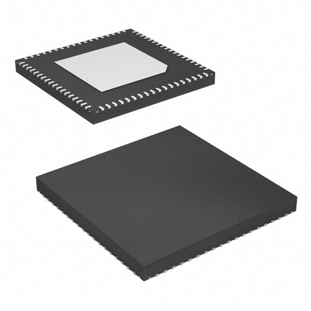
8A3xxxx 72QFN EVK User Manual
Description
Requirements
The 8Axxxx 72QFN EVK is designed to help customers evaluate
IDT ClockMatrix devices. This document discusses the following
about the EVK:
IDT Timing Commander Software Installed (available at
www.idt.com/timingcommander)
Introduces the board and its power supply and jumper settings
Describes the input and output connectors for normal
operation
USB 2.0 or USB 3.0 interface
Explains how to bring up the board using the Timing
Commander software GUI
Memory: Minimum 512MB; recommended 1GB
ClockMatrix GUI (available at www.idt.com/clockmatrix)
Windows XP SP3 or later
Processor: Minimum 1GHz
Available disk space: Minimum 600MB (1.5GB 64-bit);
recommended 1GB (2GB 64-bit)
Network access during installation if the .NET framework is
not currently installed on the system
Discusses how to configure and program the board to
generate standard-compliant frequencies
Kit Contents
8A34xxx 72QFN Evaluation Board
USB Type A cable
8A3xxxx 72QFN EVK Board
© 2019 Integrated Device Technology, Inc.
1
February 14, 2019
�8A3xxxx 72QFN EVK User Manual
Important Notes
Disclaimer
Integrated Device Technology, Inc. and its affiliated companies (herein referred to as “IDT”) shall not be liable for any damages arising out of defects resulting from
(i)
delivered hardware or software
(ii)
non-observance of instructions contained in this manual and in any other documentation provided to user, or
(iii) misuse, abuse, use under abnormal conditions, or alteration by anyone other than IDT.
TO THE EXTENT PERMITTED BY LAW, IDT HEREBY EXPRESSLY DISCLAIMS AND USER EXPRESSLY WAIVES ANY AND ALL WARRANTIES, WHETHER
EXPRESS, IMPLIED, OR STATUTORY, INCLUDING, WITHOUT LIMITATION, IMPLIED WARRANTIES OF MERCHANTABILITY AND OF FITNESS FOR A
PARTICULAR PURPOSE, STATUTORY WARRANTY OF NON-INFRINGEMENT, AND ANY OTHER WARRANTY THAT MAY ARISE BY REASON OF USAGE
OF TRADE, CUSTOM, OR COURSE OF DEALING.
!
Important Equipment Warning: Ensure the correct connection of all cables. Supplying the board using the wrong
polarity could result in damage to the board and/or the equipment. Check that all jumpers have been removed from
the board before applying power.
Contents
1.
Usage Guide.................................................................................................................................................................................................4
1.1 Board Overview ...................................................................................................................................................................................4
1.2 Board Power Supply ............................................................................................................................................................................5
1.3 Voltage Selection Jumpers ..................................................................................................................................................................5
1.4 GPIO Switches, LEDs, and Test Points ..............................................................................................................................................6
1.5 USB Jack .............................................................................................................................................................................................7
1.6 I2C between FTDI, CM Device, and Onboard EEPROM .....................................................................................................................7
2.
Working with Timing Commander™ for Programing/Configuration ..............................................................................................................8
2.1 Default Operation ................................................................................................................................................................................8
2.2 Using Timing Commander to Control the Board ..................................................................................................................................9
2.3 Output Terminations and Rework to Take 1PPS Input ......................................................................................................................15
3.
How to Upload Firmware to the RAM .........................................................................................................................................................16
4.
Schematics .................................................................................................................................................................................................18
5.
Ordering Information...................................................................................................................................................................................18
6.
Revision History..........................................................................................................................................................................................18
© 2019 Integrated Device Technology, Inc.
2
February 14, 2019
�8A3xxxx 72QFN EVK User Manual
List of Figures
Figure 1. Overview of 72QFN ClockMatrix Evaluation Board .............................................................................................................................4
Figure 2. Example of Voltage Jumpers ...............................................................................................................................................................5
Figure 3. GPIO Setting and Status Display Area ................................................................................................................................................7
Figure 4. Board Setting for Default Operation ....................................................................................................................................................8
Figure 5. Starting Up Timing Commander GUI ...................................................................................................................................................9
Figure 6. Selecting 8A34001 using Personality File v4.6..................................................................................................................................10
Figure 7. Timing Commander GUI with a Settings File Opened .......................................................................................................................11
Figure 8. Setting I2C for Connecting the Board with GUI ..................................................................................................................................12
Figure 9. A Green Band appears when a Valid Connection is Made................................................................................................................12
Figure 10. Firmware Version Mismatch Warning Message ................................................................................................................................13
Figure 11. Reading Firmware Version ................................................................................................................................................................13
Figure 12. Read Firmware Version of ClockMatrix Chip .....................................................................................................................................14
Figure 13. AC Coupling and Terminations for Input Clock..................................................................................................................................15
Figure 14. Configuring CLK0 as CMOS to Receive a 1PPS Input......................................................................................................................15
List of Tables
Table 1.
GPIO Settings......................................................................................................................................................................................6
Table 2.
EEPROM I2C Connections ..................................................................................................................................................................7
© 2019 Integrated Device Technology, Inc.
3
February 14, 2019
�8A3xxxx 72QFN EVK User Manual
1. Usage Guide
1.1 Board Overview
The following diagram identifies various components of the board: input and output SMA connectors, power supply jacks, and some jumper
settings necessary for the board operations.
Figure 1.
Overview of 72QFN ClockMatrix Evaluation Board
Detailed descriptions of the board are as follows:
Input SMA Connectors – There are five differential inputs labeled CLK0/nCLK0–CLK4/nCLK4. Each input clock can be configured
differentially (LVDS, PECL 2.5V, and PECL 3.3V) or in single-ended format (CMOS).
Output SMA Connectors – There are 12 outputs labeled as Q0/nQ0–Q11/nQ11. Each output clock can be configured differentially (LVDS,
LVPECL, or user-defined amplitude) or in single-ended format (LVCMOS – in-phase or out-of-phase).
GPIO switch, LEDs, and test points – There are seven GPIOs available. Each GPIO can be set a “low” or “high” level (if input) or
displayed with an LED (if output). Some GPIOs are used to set the chip in a certain working condition on power-up. For more information,
see GPIO Switches, LEDs, and Test Points.
USB connector – A USB mini connector connects the evaluation board to a PC for GUI communications. No power is drawn from the USB
connector other than to power the FTDI USB chip.
© 2019 Integrated Device Technology, Inc.
4
February 14, 2019
�8A3xxxx 72QFN EVK User Manual
VDDQx voltage selection jumpers – Each output voltage can be individually supplied with 1.8V, 2.5V, or 3.3V. These jumpers are used to
select the voltage for the output voltages.
Reset button – A small button is used to reset the board.
OSCI Input connector – An SMA connector, J45, can optionally supply a clock signal to overdrive the crystal.
Optional OCXO/TCXO Reference – An OCXO/TCXO footprint, is output at J82. It can be connected to J46 (below) as the reference for
the System DPLL.
SysDPLL Input – An SMA connector, J46, is provided to supply a local OCXO/TCXO reference as an optional reference for the System
DPLL.
Crystal – A crystal of various frequencies must be present for board operations. A 3225 footprint is provided for SMT crystals. For easy
plug-in of a canned crystal, two through holes are also available.
EEPROM – An SO-8 socket is provided to hold an EEPROM device of compatible package. An EEROM is used to store firmware and
customer configuration data, if needed.
1.2 Board Power Supply
The board uses a single +5V supply for its power supplies. When running the board, please set the bench power supply at 5V/2A. The red jack
(J1) is positive; the black jack (J2) is the ground.
Multiple LDOs are used to generate 3.3V, 2.5V, and 1.8V from the +5V supply.
1.3 Voltage Selection Jumpers
There are eight headers/jumpers to select different voltages for different functional blocks of the chip. Each header has pin 1 and 3 labeled in
silkscreen – jumping pin 1 and pin 2 will select 3.3V; jumping pin 2 and pin 3 will select 2.5V; no jumper will have 1.8V.
Please see the following example for JP4 and JP9 – JP4 will select 2.5V; JP9 will select 3.3V.
Figure 2.
Example of Voltage Jumpers
© 2019 Integrated Device Technology, Inc.
5
February 14, 2019
�8A3xxxx 72QFN EVK User Manual
The following list shows which head/jumper is used to select what voltage:
JP1 – VDDD
JP2 – VDDA
JP3 – VCC_GPIO_DC
JP4 – VDDO_Q8_3_5
JP5 – VDDO_Q2_4_11
JP6 – VDDO_1_10_7
JP7 – VDD_CLK0
JP9 – VDDO_Q0_9_6
Important Equipment Warning: VDD_FOD voltage is selected by resistors R908 and R909. In order to prevent
damage to the device, both R908 and R909 should not be stuffed, in which case VDD_FOD = 1.8V.
!
1.4 GPIO Switches, LEDs, and Test Points
An 8-bit dip switch sets the logic levels for seven GPIOs (GPIO0-5 and GPIO9). The following table shows the GPIO levels for each setting and
the corresponding LED state.
Table 1.
GPIO Settings
Dip Switch Position
GPIO Logic Level
LED
Left
Low
On
Center
High if GPIO is configured as Input
High or Low according to the GPIO output setting
High if GPIO is configured as Input
High or Low according to the GPIO output setting
Right
High
Off
Please see the picture and labels in Figure 3.
When the GPIOs are configured as outputs (such as User-Controlled or LOL indicator), the dip switch for the corresponding GPIO should be
placed in the center position. The LED will indicate the state of the GPIO.
© 2019 Integrated Device Technology, Inc.
6
February 14, 2019
�8A3xxxx 72QFN EVK User Manual
Figure 3.
GPIO Setting and Status Display Area
1.5 USB Jack
The board has a USB mini-connector. The other end of the USB cable is a USB Type A connector going to a PC.
1.6 I2C between FTDI, CM Device, and Onboard EEPROM
One of the major differences between the 72QFN and 144BGA144 chips is that there is only one serial bus on the 72QFN chip. The I2C bus
between the FTDI chip and CM chip is the same bus between the CM chip and the onboard EEPROM. The onboard EEPROM is used to store
device firmware and/or customer’s configuration data. JP12 and JP13 must be jumped between pin 1 and 2 to enable the I2C connections.
Table 2.
EEPROM I2C Connections
JP12/JP13
JP12/JP13
Jumper Position
Pin 1 and 2
Pin 2 and 3
EEPROM I2C Path
FDTI and CM Chip;
CM Chip and EEPROM
N/A
© 2019 Integrated Device Technology, Inc.
7
February 14, 2019
�8A3xxxx 72QFN EVK User Manual
2. Working with Timing Commander™ for Programing/Configuration
The following sections are best cross-referenced with the ClockMatrix GUI Step-by-Step User Guide which is available on www.idt.com.
2.1 Default Operation
The board can operate off an EEPROM that has stored all information including firmware and a default configuration data. A default operation
provides a sanity check on the board before running the board through the IDT Timing Commander. Please set the board in the following default
conditions (see Figure 4 for jumper and switch positions).
Set all the GPIOs to the center position. This will ensure that GPIO9 is high and that the serial port is configured for I2C 1-byte
addressing.
VDDA = 3.3V, VDD_ FOD = 1.8V, and VDDO_Qx = 3.3V
Crystal frequency = 50MHz
CLK0 = 25MHz
FTDI, CM device, and EEPROM share the same I2C bus by jumping Pin 1 and 2 of JP12 and JP13
With the above default conditions ready, connect the board to the PC using a USB type A to USB mini cable, and power up the board using a
single +5V supply. On power-up, the ClockMatrix chip will read its firmware and configuration data from EEPROM and update all registers.
When this process is completed, the following frequencies are available:
Q0 = 122.88MHz
Q1 = 122.88MHz
Figure 4.
!
Board Setting for Default Operation
Important Equipment Warning: In order to set GPIO9 to “High”, the switch for GPIO9 must be set either to the “+”
(high) position or the center position.
© 2019 Integrated Device Technology, Inc.
8
February 14, 2019
�8A3xxxx 72QFN EVK User Manual
2.2 Using Timing Commander to Control the Board
Once the default operation is successful, complete the following steps to configure and program the ClockMatrix device per your specific
application requirements using Timing Commander GUI tools:
1.
Power up the board and set the main serial port in I2C mode by GPIO9 = “high”. Connect the board to the PC.
2.
Start the Timing Commander software. You will see options of “New Setting File” and “Open Setting file”. For a new configuration, select
“New Setting File”.
Figure 5.
Starting Up Timing Commander GUI
© 2019 Integrated Device Technology, Inc.
9
February 14, 2019
�8A3xxxx 72QFN EVK User Manual
3.
After selecting “New Settings File”, a device selection window will pop up. In the window, choose the intended device in the list (in this
example, 8A34001 is selected). Click the button at the lower right corner of the window (red circle) to browse and select the correct
personality file (in this example, personality v4.6 is selected). Click OK.
Figure 6.
Selecting 8A34001 using Personality File v4.6
© 2019 Integrated Device Technology, Inc.
10
February 14, 2019
�8A3xxxx 72QFN EVK User Manual
4.
The GUI window with the 8A34001 block diagram will open for configurations; or if “Open Settings File” is selected in Step 3, you will be
prompted to browse and select an existing .tcs file and the personality file. When the configuration file is open, all configured values will be
displayed (see Figure 7).
Figure 7.
Timing Commander GUI with a Settings File Opened
© 2019 Integrated Device Technology, Inc.
11
February 14, 2019
�8A3xxxx 72QFN EVK User Manual
5.
In order to connect the board with Timing Commander (PC), click the button (red circle) at the up-right corner of the GUI to set up the
communication protocols (see Figure 7).
After I2C and one-byte addressing are selected, click OK to close the window.
Figure 8.
6.
Setting I2C for Connecting the Board with GUI
Click on the chip symbol at the upper-right corner to initiate the connection. The connection is valid when a green band appears at the
upper-right corner of the window, as shown below.
Figure 9.
A Green Band appears when a Valid Connection is Made
© 2019 Integrated Device Technology, Inc.
12
February 14, 2019
�8A3xxxx 72QFN EVK User Manual
7.
If ClockMatrix chip’s firmware, or firmware loaded from EEPROM, has a different version from that in the Personality file, a firmware version
mismatch warning message will appear. Click “Close” button to close the message window and a connection is made.
Figure 10. Firmware Version Mismatch Warning Message
8.
Once the connection is made, the firmware version can be read within the GUI. Click the “Firmware Utility” button to bring up the Firmware
Utility window, as shown below.
Figure 11. Reading Firmware Version
© 2019 Integrated Device Technology, Inc.
13
February 14, 2019
�8A3xxxx 72QFN EVK User Manual
9.
Within the Firmware Utility window, click the “Get Firmware Version” button to read the firmware version.
Figure 12. Read Firmware Version of ClockMatrix Chip
10. In the case where the firmware version mismatches each other, a firmware upgrade is necessary to update the chip’s firmware. To do so,
complete the steps in How to Upload Firmware (see Section 3) to update the chip’s firmware.
© 2019 Integrated Device Technology, Inc.
14
February 14, 2019
�8A3xxxx 72QFN EVK User Manual
2.3 Output Terminations and Rework to Take 1PPS Input
All outputs are terminated with a 100Ω resistor across the output pair. This is the recommended termination regardless of the Voffset and
Vswing settings. Since the outputs are DC-coupled, they will support a 1PPS output without any need for rework.
!
Important Equipment Warning: When connecting the outputs to measurement equipment, use a DC-block to ensure
that the output operates at its intended Voffset. Otherwise, the equipment may load the output down and cause degraded
performance.
The following rework must be implemented in order to support a 1PPS input clock. All input clocks for this board are ac-coupled and terminated
as in the following figure.
Figure 13. AC Coupling and Terminations for Input Clock
For a 1PPS input, a single-ended input with DC-coupling is recommended. As such, the populated AC-coupling capacitor must be removed
and the input must be configured as LVCMOS, not differential.
1.
In Figure 13, to make CLK0 supportive of 1PPS input, first configure CLK0 as LVCMOS in Timing Commander (see Figure 14).
Figure 14. Configuring CLK0 as CMOS to Receive a 1PPS Input
2.
Once in LVCMOS mode, CLK0_P and CLK0_N will be two separate LVCMOS inputs instead of a differential pair. To make CLK0_P receive
a 1PPS input, replace C881 with a 0Ω resistor; and at the same time, remove R765 and R770.
© 2019 Integrated Device Technology, Inc.
15
February 14, 2019
�8A3xxxx 72QFN EVK User Manual
3. How to Upload Firmware to the RAM
1. Connect to the EVK board.
2. Power up the board with no EEPROM present. This ensures the firmware is 4.0.2.7017, as displayed in the figure.
3. The GUI will indicate that the firmware on the chip does not match the GUI firmware. Press “Close”.
4.
Open the “Firmware Utility” window by clicking on the button as follows.
5.
Update the Firmware first. Press “Update RAM to Current FW Only”.
6.
In the next window, press “Yes” and wait around 3-4 minutes.
© 2019 Integrated Device Technology, Inc.
16
February 14, 2019
�8A3xxxx 72QFN EVK User Manual
7.
Once the firmware is updated, the following window will indicate a successful update. Click “Close”.
8.
Press “Get Firmware Version” to verify that the RAM was updated correctly, then click “Close”.
© 2019 Integrated Device Technology, Inc.
17
February 14, 2019
�8A3xxxx 72QFN EVK User Manual
4.
Schematics
Please see the schematics located at the end of this document.
5. Ordering Information
Orderable Part Number
8A34044-EVK
Description
8A3xxxx 72QFN Evaluation Kit
6. Revision History
Revision Date
February 14, 2019
Description of Change
Initial release.
Corporate Headquarters
Sales
Tech Support
6024 Silver Creek Valley Road
San Jose, CA 95138
www.IDT.com
1-800-345-7015 or 408-284-8200
Fax: 408-284-2775
www.IDT.com/go/sales
www.IDT.com/go/support
DISCLAIMER Integrated Device Technology, Inc. (IDT) and its affiliated companies (herein referred to as “IDT”) reserve the ri ght to modify the products and/or specifications described herein at any time,
without notice, at IDT's sole discretion. Performance specifications and operating parameters of the described products are determine d in an independent state and are not guaranteed to perform the same
way when installed in customer products. The information contained herein is provided without representation or warranty of any kind, whether express or implied, including, but not limite d to, the suitability
of IDT's products for any particular purpose, an implied warranty of merchantability, or non -infringement of the intellectual property rights of others. This document is presented only as a guide and does not
convey any license under intellectual property rights of IDT or any third parties.
IDT's products are not intended for use in applications involving extreme environmental conditions or in life support systems or similar devices where the failure or malfunction of an IDT pro duct can be
reasonably expected to significantly affect the health or safety of users. Anyone using an IDT product in such a manner does so at their own risk, absent an express, written agreement by IDT.
Integrated Device Technology, IDT and the IDT logo are trademarks or registered trademarks of IDT and its subsidiaries in the United States and other countries. Other trademarks used herein are the
property of IDT or their respective third party owners. For datasheet type definitions and a glossary of common terms, visit www.idt.com/go/glossary. All contents of this document are copyright of Integrated
Device Technology, Inc. All rights reserved.
© 2019 Integrated Device Technology, Inc.
18
February 14, 2019
�5
4
3
2
1
D
D
C
C
B
B
PROJECT NAME
Fidus Systems
A
Indira3
DESIGN
DB
DRAWN
DB
CHECK
DB
5
4
3
2
A
375 Terry Fox Drive, Ottawa, ON K2K 0J8
TITLE
IDT8A34001
SUBTITLE
Block Diagram
DRAWING NUMBER
REVISION
SK-10280-01
1.2
RELEASE DATE
SHEET
1 OF
27 October 2016
1
9
�5
4
3
2
1
D
D
VDDO_Q3
VDDO_Q2
VDDO_Q1
VDDO_Q0
VDDO_Q8
VDD_FOD_0
CLK_Q8_P
CLK_Q8_N
8
8
CLK_Q0_P
CLK_Q0_N
8
8
CLK_Q1_P
CLK_Q1_N
8
8
CLK_Q2_P
CLK_Q2_N
C761
GPIO0
GPIO4
GPIO5
C
DNS
2.67k
2.67k
OSCO
OSCI
VDD_FOD_0
VDD_CLK0_0
TST_CHIP_RST_N_OD
CLK_CLK0_P
CLK_CLK0_N
CLK_CLK1_P
CLK_CLK1_N
CLK_CLK2_P
CLK_CLK2_N
CLK_CLK3_P
CLK_CLK3_N
DNS
R466
49.9
1
2
3
4
5
6
7
8
9
10
11
12
13
14
15
16
17
18
0
19-03-13 RK
5-1814832-1
OSCO
OSCI
VDDD
VDDD_0
C694
C695
10uF
0.1uF
0.1uF
0.1uF
C871 0.1uF
C693
R392
C692
0
CLK_CLK4_P
CLK_CLK4_N
OSCO
OSCI
72
71
70
69
68
VDD_DIA_FOD_A 67
66
VDDO_Q0
Q0 65
nQ0 64
63
GPIO4
nQ1 62
Q1 61
60
VDDO_Q1
59
VDDO_Q2
58
Q2
57
nQ2
56
GPIO5
55
VDDO_Q3
DNS
R934
R467
SILKSCRN:
XO_DPLL
R910
J46
VDDA_0
cREG_XTAL
GPIO0
nQ8
Q8
VDDO_Q8
U409
VDD_FOD
Q3
nQ3
VDDO_Q9
Q9
nQ9
GPIO1
VDD_GPIO_FOD
GPIO2
nQ10
Q10
VDDO_Q10
nQ4
Q4
VDDO_Q4
nQ5
Q5
VDDO_Q5
VDDO_Q6
VDDA_PDCP_XTAL
VDDA_FB
nMR
VDD_CLK
XO_DPLL
CLK0
nCLK0
CLK1
nCLK1
CLK2
nCLK2
CLK3
nCLK3
VDD_DIG
CLK4
nCLK4
SCLK
SDIO
SDI_A1
CS_A0
FILTER
VDDA_LC_BG
nTEST
GPIO3
nQ11
Q11
VDDO_Q11
VDD_DIA_FOD_B
VDDO_Q7
Q7
nQ7
GPIO9
nQ6
Q6
Maximum voltage on pin 7 = 1.8V
73
EPAD
10uF
C
8
8
5
5
5
54
53
52
51
50
49
48
47
46
45
44
43
42
41
40
39
38
37
CLK_Q3_P
CLK_Q3_N
8
8
CLK_Q9_P
CLK_Q9_N
GPIO1
5
8
8
GPIO2
5
CLK_Q10_N
CLK_Q10_P
VDDO_Q9
VDD_FOD_5
8
8
CLK_Q4_N
CLK_Q4_P
8
8
CLK_Q5_N
CLK_Q5_P
8
8
VDDO_Q10
VDDO_Q4
VDDO_Q5
VDDO_Q6
IDT8A35018
B
19
20
21
22
23
24
25
26
27
28
29
30
31
32
33
34
35
36
B
PLL_I2C_SCL_SCLK
PLL_I2C_SDA_SDIO
PLL_I2C_SDA_SDI
PLL_I2C_SDA_CSN
CLK_Q6_P
CLK_Q6_N
8
8
CLK_Q7_P
CLK_Q7_N
8
8
CLK_Q11_P
CLK_Q11_N
VDDA_1
C763
C762
R456
8
8
JTAG_SEL
C418
0.1uF
DNS
0.1uF
DNS
0
VDD_FOD_2
GPIO3
5
GPIO9
5
2200pF
VDDO_Q11
VDDO_Q7
Place close to ClockMatrix
A
A
Title
Size
C
Date:
5
4
3
2
Document Number
Rev
Monday, May 21, 2018
Sheet
1
1
of
1
�5
4
3
2
1
5V0
Board 3V3
VDDD
D
5V0
3
2
GND
GNDPAD
6
9
C838
C841
C842
0.01uF 0.1uF 10uF
R598 10k
1000pF
10uF
SILKSCRN:
3V3
C865
C863
SILKSCRN:
3.3V Top
2.5V Bot
1.8V Float
C864
GND
GND
DAP
9
26.1k
0.01uF 0.1uF 10uF
8
D
JP1
R709
6
7
13
3V3
21k
R708
02-09-15 RvR
LP38798SD-ADJ/NOPB
IC REG LDO ADJ 0.8A 12WSON
SILKSCRN:
VDDD
2V5
44.2k
1V8/FPGA
R707 52.3k
D16
LNJ347W83RA
D3
LNJ347W83RA
CP
FB
03-09-15 RvR
ADM7171ACPZ-R7
IC REG LDO ADJ 1A 8LFCSP
SET
4
10
11
12
R706
EN
C867
0.01uF
SS
3
C866
SENSE
5
1.0uF
C836
3k
C837
0.01uF 0.1uF 10uF
EN
1
2
IN
OUT_FB
IN
OUT
IN_CP
OUT
1k
4
VOUT
VOUT
R597
5
VIN
VIN
17.4k
C846
R486
C845
111-0703-001
POST BINDING INSUL GROUNDED BLCK
C3
19-02-14 RvR
D1
1
1
NC
J2
RvR 19-11-14
111-0702-001
POST BINDING INSULATED RED
BZX84C5V6
DIODE ZENER 5.6V 350MW SOT23-3
19-02-14 RvR
7
8
1
1
R599
1
U69
1206L350SLTHYR
1
2
3
10k
J1
RT1
U70
R703
3V3
VDDA_SEL
SILKSCRN:
5V
C
C
5V0
5V0
5
EN
SET
4
R15
C800
0.01uF 0.1uF 10uF
26.1k
8
5
4
JP2
R18
1V8/FPGA
VDDA_SEL
02-09-15 RvR
LP38798SD-ADJ/NOPB
IC REG LDO ADJ 0.8A 12WSON
EN
SET
CP
FB
GND
GND
DAP
10
11
12
9
C14
R29
26.1k
C803
SILKSCRN:
3.3V Top
2.5V Bot
1.8V Float
C804
0.01uF 0.1uF 10uF
8
JP3
R77
6
7
13
R76
R30
SILKSCRN:
VDDA
2V5
44.2k
IN
OUT_FB
IN
OUT
IN_CP
OUT
0.01uF
R17
3V3
21k
1.0uF
6
7
13
R16
1.0uF
0.01uF
GND
GND
DAP
9
C799
VCC_GPIO_DC
U17
1
2
3
C16
FB
C8
SILKSCRN:
3.3V Top
2.5V Bot
1.8V Float
C15
C10
C9
CP
10
11
12
10k
10k
IN
OUT_FB
IN
OUT
IN_CP
OUT
R26
R12
VDDA
U9
1
2
3
3V3
21k
SILKSCRN:
VCC_GPIO_DC
2V5
44.2k
1V8/FPGA
VDDA_SEL
02-09-15 RvR
52.3k
52.3k
LP38798SD-ADJ/NOPB
IC REG LDO ADJ 0.8A 12WSON
B
B
5V0
VDD_FOD
R902
U89
1
2
3
10k
5
4
IN
OUT_FB
IN
OUT
IN_CP
OUT
EN
SET
FB
R903
C953
C954
0.1uF
10uF
SILKSCRN:
VDD_FOD
26.1k
R904
NP
8
R905 NP
NP
DNS
Stuff for 3.3V
R909
52.3k
A
NP
DNS
02-09-15 RvR
LP38798SD-ADJ/NOPB
IC REG LDO ADJ 0.8A 12WSON
Stuff for 2.5V
6
7
13
R908
GND
GND
DAP
9
R907
C957 0.01uF
C956 1.0uF
CP
10
11
12
PROJECT NAME
DESIGN
DB
DRAWN
DB
CHECK
DB
5
4
Fidus Systems
Indira3
3
2
A
375 Terry Fox Drive, Ottawa, ON K2K 0J8
TITLE
IDT8A34001
SUBTITLE
Power Supplies 1
DRAWING NUMBER
REVISION
SK-10280-01
1.2
RELEASE DATE
SHEET
2 OF
27 October 2016
1
9
�5
4
3
2
1
D
D
5V0
5V0
VDDO_Q8_3_5
R40
SILKSCRN:
3.3V Top
2.5V Bot
1.8V Float
U19
10k
5
EN
SET
C22
C21
CP
FB
9
C20
R43
26.1k
C810
C811
0.01uF 0.1uF 10uF
R84
21k
44.2k
3V3
SILKSCRN:
VDDO_Q8,Q3,Q5
2V5
5
4
VDDA_SEL
IN
OUT_FB
IN
OUT
IN_CP
OUT
EN
SET
CP
FB
10
11
12
9
C29
R64
26.1k
C814
SILKSCRN:
3.3V Top
2.5V Bot
1.8V Float
C815
JP5
0.01uF 0.1uF 10uF
R503
21k
3V3
SILKSCRN:
VDDO_Q2,Q4,Q11
8
R501
6
7
13
44.2k
2V5
VDDA_SEL
R65
GND
GND
DAP
0.01uF
1.0uF
02-09-15 RvR
52.3k
LP38798SD-ADJ/NOPB
IC REG LDO ADJ 0.8A 12WSON
C31
C30
6
7
13
VDDO_Q2_4_11
U22
1
2
3
JP4
R85
8
R35
0.01uF
1.0uF
GND
GND
DAP
10
11
12
10k
4
IN
OUT_FB
IN
OUT
IN_CP
OUT
R61
1
2
3
02-09-15 RvR
52.3k
LP38798SD-ADJ/NOPB
IC REG LDO ADJ 0.8A 12WSON
C
C
5V0
5V0
EN
SET
FB
SILKSCRN:
3.3V Top
2.5V Bot
1.8V Float
R57
26.1k
C817
0.01uF 0.1uF 10uF
R92
21k
3V3
5
SILKSCRN:
VDDO_Q1,Q10,Q7
44.2k
2V5
EN
SET
CP
FB
GND
GND
DAP
10
11
12
9 R401
C402
26.1k
C403
C404
0.01uF 0.1uF 10uF
R403
JP7
3V3
21k
8
R404
6
7
13
SILKSCRN:
3.3V Top
2.5V Bot
1.8V Float
SILKSCRN:
VDD_CLK0
VDDA_SEL
52.3k
02-09-15 RvR
LP38798SD-ADJ/NOPB
IC REG LDO ADJ 0.8A 12WSON
52.3k
02-09-15 RvR
LP38798SD-ADJ/NOPB
IC REG LDO ADJ 0.8A 12WSON
2V5
44.2k
R402
VDDA_SEL
4
IN
OUT_FB
IN
OUT
IN_CP
OUT
0.01uF
1.0uF
6
7
13
VDD_CLK0
U400
1
2
3
JP6
R93
8
R58
0.01uF
1.0uF
GND
GND
DAP
9
C816
C401
C28
C27
CP
C26
C400
4
10
11
12
10k
10k
5
IN
OUT_FB
IN
OUT
IN_CP
OUT
R400
R55
VDDO_Q1_10_7
U21
1
2
3
B
B
5V0
TP1
VDDO_Q0_9_6
R47
1
2
3
10k
5
4
C25
C24
A
SILKSCRN:
3.3V Top
2.5V Bot
1.8V Float
U20
IN
OUT_FB
IN
OUT
IN_CP
OUT
EN
SET
CP
FB
9
C23
R50
26.1k
C812
C813
JP9
0.01uF 0.1uF 10uF
R89
21k
3V3
8
R88
6
7
13
44.2k
SILKSCRN:
VDDO_Q0,Q9,Q6
2V5
PROJECT NAME
DESIGN
02-09-15 RvR
DB
52.3k
LP38798SD-ADJ/NOPB
IC REG LDO ADJ 0.8A 12WSON
DRAWN
DB
CHECK
DB
5
Fidus Systems
Indira3
4
3
2
A
375 Terry Fox Drive, Ottawa, ON K2K 0J8
VDDA_SEL
R51
0.01uF
1.0uF
GND
GND
DAP
10
11
12
TITLE
IDT8A34001
SUBTITLE
Power Supplies 2
DRAWING NUMBER
REVISION
SK-10280-01
1.2
RELEASE DATE
SHEET
3 OF
27 October 2016
1
9
�5
4
3
2
1
D
D
3V3
0.1uF
VPLL
Y1
B
13
OSCI
OSCO
AGND
TEST
12pF
12pF
GND
GND
C691
C690
2
3
3
6
R385
60
36
REF
PWREN_N
GND
GND
GND
GND
GND
GND
GND
GND
SUSPEND_N
GND_PAD
3V3
R424
1k
38
39
40
41
43
44
45
46
VCCB
A1
A2
A3
A4
B1
B2
B3
B4
14
13
12
11
10
CLK_FTDI_PLL_SCL_OD
FTDI_PLL_SDA_OD
6
48
52
53
54
55
57
58
59
C
OE
NC1
GND
NC2 GND_PAD
7
15
08-10-14 EM
TXB0104RGYR
IC VOLT-LEVEL TRANSLATOR 14-QFN
3V3
VCC_GPIO_DC
DNS U404
1
2
3
4
5
8
3V3
R425
1k
10
1
5
11
15
25
35
47
51
6
C413 0.1uF
EECS
EECLK
EEDATA
BCBUS0
BCBUS1
BCBUS2
BCBUS3
BCBUS4
BCBUS5
BCBUS6
BCBUS7/PWRSAV_N
26
27
28
29
30
32
33
34
6
9
0.1uF
R381
RESET_N
8
VCCA
C412
DATA_P
DATA_N
BDBUS0
BDBUS1
BDBUS2
BDBUS3
BDBUS4
BDBUS5
BDBUS6
BDBUS7
2
3
4
5
0
DNS
0
DNS
63
62
61
24-07-13 RK
U403
1
33
33
R423
VPHY
ACBUS0
ACBUS1
ACBUS2
ACBUS3
ACBUS4
ACBUS5
ACBUS6
ACBUS7
R410
R411
R422
EM 06-02-13
ABM8G-12.000MHZ-18-D2Y-T
CRYSTAL 12.0000MHZ 20PPM 4SMD
0.1uF
0.1uF
VREGOUT
VREGIN
ADBUS0
ADBUS1
ADBUS2
ADBUS3
ADBUS4
ADBUS5
ADBUS6
ADBUS7
16
17
18
19
21
22
23
24
C411 0.1uF
C410
C42
0.1uF
14
1k
2
4
4.7k
3.3uF
C41
8
7
1
4.7k
C46
0.1uF
0.1uF
3
2
548190589
CONN RCPT USB MINI-B 5POS RA SMT
0
VCCIO
VCCIO
VCCIO
VCCIO
4
R382
R421
C45
C40
ID
0.1uF
DATA_P
DATA_N
9
VCORE
VCORE
VCORE
0.1uF
GND
GND_SHLD
GND_SHLD
GND_SHLD
GND_SHLD
1
4.7uF
VBUS
49
50
4
C685
J17
5
6
7
8
9
20
31
42
56
L83
220
VCC_GPIO_DC
U1
12
37
64
C48
TPD4S012DRYR
IC 4CH ESD SOLUTION W/CLAMP 6SON
D2
LNJ347W83RA
0.1uF
ADM7171ACPZ-R7
IC REG LDO ADJ 1A 8LFCSP
L84
220
4.7uF
10uF
03-09-15 RvR
SILKSCRN:
USB PWR
0.1uF
6
9
C39
3
C684
GND
GNDPAD
C47
SENSE
SS
R383
10k
3
ID
DB 24-07-14
1000pF
GND
10uF
1
2
USBD_P
USBD_N
C686
4
NC
C687
5
4
C688
6
1
2
R384
17.4k
EN
U55
VBUS
VOUT
VOUT
C38
5
VIN
VIN
R474
1k
7
8
C44
USB 3V3
U57
0.1uF
C
C43
3V3_FTDI
R420
1V8_FTDI
5V0_USB
3V3
6
9
VCCA
VCCB
A1
A2
A3
A4
B1
B2
B3
B4
14
13
12
11
10
SPI_SCLK
SPI_SDIO
SPI_SDI
SPI_CSN
6
6
6
6
OE
B
NC1
GND
NC2 GND_PAD
7
15
08-10-14 EM
SPI_SDIO
J4
1
3
5
7
9
1
3
5
7
9
2
4
6
8
10
2
4
6
8
10
TXB0104RGYR
IC VOLT-LEVEL TRANSLATOR 14-QFN
18-03-13 RK
65
12k
N2510-6V0C-RB-WD
CONN HEADER 10POS SMT VERT 30AU
16-08-13 RK
FT2232HQ-REEL
IC USB HS DUAL UART/FIFO 64-QFN
Notes:
1. By connecting I2C to the header's pin 1 and 3, this is
to give I2C access to external I2C master;
2. By installing R926 and R927, FTDI can also access Aux
I2C port (also removing R87 and R88). This feature is not
expected to be used.
3. Normal use: FTDI controls I2C port; Header is connected
to Aux port in SPI configuration.
PROJECT NAME
Fidus Systems
A
Indira3
DESIGN
DB
DRAWN
DB
CHECK
DB
5
4
3
2
A
375 Terry Fox Drive, Ottawa, ON K2K 0J8
TITLE
IDT8A34001
SUBTITLE
FTDI USB Interface
DRAWING NUMBER
REVISION
SK-10280-01
1.2
RELEASE DATE
SHEET
4 OF
27 October 2016
1
9
�5
4
3
2
1
Note for Silkcreen:
Place GPIO[x] lable close to each
corresponding LED and Test point.
D
D
VCC_GPIO_DC
R487
1k
VCC_GPIO_DC
D4
R488
1k
GPIO[0]
VCC_GPIO_DC
D5
TP2
GPIO0
6
GPIO1
6
GPIO2
6
GPIO3
6
GPIO4
6
GPIO5
D6
R492
1k
GPIO[2]
GPIO[3]
D7
TP4
LNJ347W83RA
TP5
LNJ347W83RA
LNJ347W83RA
GPIO0
GPIO0
GPIO1
GPIO2
GPIO3
GPIO1
GPIO2
GPIO3
GPIO4
VCC_GPIO_DC
VCC_GPIO_DC
GPIO5
R495
1k
D8
R496
1k
GPIO[4]
D9
TP6
GPIO[5]
TP7
LNJ347W83RA
LNJ347W83RA
GPIO4
6
R491
1k
GPIO[1]
TP3
LNJ347W83RA
6
VCC_GPIO_DC
GPIO5
GPIO9
GPIO9
C
C
VCC_GPIO_DC
R500
1k
D11
GPIO[9]
TP11
LNJ347W83RA
GPIO9
VCC_GPIO_DC
SILKSCRN:
H
L
U405
1
2
3
4
5
6
7
8
B
VCC
nc1
nc2
nc3
nc4
nc5
nc6
VEE
s1
s2
s3
s4
s5
s6
s7
s8
16
15
14
13
12
11
10
9
R426
R427
R428
R429
R430
R431
R432
1k
1k
1k
1k
1k
1k
1k
GPIO0
GPIO1
GPIO2
GPIO3
GPIO4
GPIO5
GPIO9
B
DIP_SW8
PROJECT NAME
Fidus Systems
A
Indira3
DESIGN
RK
DRAWN
RK
CHECK
DB
5
4
3
2
A
375 Terry Fox Drive, Ottawa, ON K2K 0J8
TITLE
IDT8A34001
SUBTITLE
GPIO LEDs
DRAWING NUMBER
REVISION
SK-10280-01
1.2
RELEASE DATE
SHEET
5 OF
27 October 2016
1
9
�5
4
SILKSCRN:
OSCI
J45
D
R469
R470
0
0
DNS
DNS
R471
R472
0
0
39
19-03-13 RK
C759
1.0uF
DNS
OSCI
OSCO
10
5-1814832-1
Y3
1
C765
C766
NC1
NC2
JP12~JP15 Default Jump Up
R117
CLK_FTDI_PLL_SCL_OD
33
R118
FTDI_PLL_SDA_OD
CX3225GB50000P0HPQCC
CRYSTAL 50.000MHZ 20PPM 18PF SMD
PLL_I2C_SCL_SCLK
33
JP12
0552-2-15-01-11-27-10-0
0552-2-15-01-11-27-10-0
PLL_I2C_SDA_SDIO
P1
Y2 DNS
P2
DNS
DNS
JP13
A-50.000-12-EXT
CRYSTAL 50MHZ 12PF 30PPM HC49/U
SPI Bus
EEPROM_SEL
4
SPI_SCLK
4
SPI_SDIO
4
4
15-01-16 RvR
15-01-16 RvR
EEPROM_SEL
C
10pF
2
4
25-11-15 DM
1
4
3
10pF
1
4
1
D
R468
I2 Bus
2
Place close to
crystal Y3
R473 DNS
DNS
DNS
3
SPI_SDI
SPI_CSN
R119
33
R120
33
R121
33
R122
33
C
Place sockets to
match spacing of
through-hole crystal
PLL_I2C_SDA_SDI
JP14
EEPROM_SEL
PLL_I2C_SDA_CSN
JP15
EEPROM_SEL
3V3
U407
1
2
PLL_I2C_SCL_SCLK
PLL_I2C_SDA_SDIO
RESET_N
CT
MR_N
SENSE
GND
GND_PAD
B
TST_CHIP_RST_N_OD
6
3
TST_CHIP_RST_N_OD
5
7
0.1uF
DNS
1k
VDD
C416
R449
C426
8
7
6
5
R445
8
7
6
5
4.7k
R453
R454
R455
1
2
3
4
4.7k
4.7k
0
4.7k
DNS
4.7k
DNS
0.1uF
4
P3
1
2
3
4
10k
DNS
10k
10k
R446
R447
R448
R450
R451
R452
C417
4.7k
JTAG_SEL
R443
VCC_GPIO_DC
R935
B
0.1uF
R444
VCC_GPIO_DC
VCC_GPIO_DC
R442
C415
5V0
08-04-14 EM
TPS3808G01DRVR
ADJ SUPPLY MONITOR PRG DLY 6QFN
11-11-14 RvR
2
4.7k
4.7k
2
4.7k
1
18-03-13 RK
U408DNS
8
TSM-102-01-T-SV
CONN HEADER 2POS 0.1IN PITCH SMD
7
SILKSCRN:
JUMPER IN = JTAG
SILKSCRN:
JUMPER IN = WP OFF
A08-LC-TT
IC SOCKET STRAIGHT 8POS TIN
6
5
VCC
SCL
SDA
J7
A0
A1
A2
WP
1k
1
0.01uF
J83
1
2
3
1
1
2
2
18-03-13 RK
TSM-102-01-T-SV
CONN HEADER 2POS 0.1IN PITCH SMD
SILKSCRN:
RESET
SW1
2
1
28-01-14 RvR
3
4
24LC64-I/P
IC EEPROM 64KBIT 400KHZ 8DIP
5
VSS
4
RvR 04-06-14
KMR211GLFS
SWITCH TACTILE SPST-NO 0.05A 32V
PROJECT NAME
Fidus Systems
A
Indira3
DESIGN
DB
DRAWN
DB
CHECK
DB
5
4
3
2
A
375 Terry Fox Drive, Ottawa, ON K2K 0J8
TITLE
IDT8A34001
SUBTITLE
PLL Core
DRAWING NUMBER
REVISION
SK-10280-01
1.2
RELEASE DATE
SHEET
6 OF
27 October 2016
1
9
�5
4
3
2
1
J82
3V3
TP19
Y4
C196
220
C195
C844
L97
4
1
DNS
VCC
NC
OUT
GND
3
2
R143
33
SILKSCRN:
CLK OSC
CLK_EXT_OSC
PLACE NEAR OSCILLATOR
20-03-13 RK
D
0.1uF
10uF
0.1uF
M6141LF
12.8MHZ MERC 9X7 HOT CMOS 3.3V OCXO
D
RK 19-03-13
5-1814832-1
VDD_CLK0
VDD_CLK0
R912
0
C882
1.0uF
19-03-13 RK
5-1814832-1
J20
CLK_CLK0_N
49.9
19-03-13 RK
C883
1.0uF
5-1814832-1
J63
C884
1.0uF
R915 49.9
CLK_CLOCK4_N
5-1814832-1
CONN SOCKET SMA STR DIE CAST PCB
CLK_CLK4_P
CLK_CLK4_N
2.67k
2.67k
19-03-13 RK
5-1814832-1
CLK_CLOCK4_P
R774
SILKSCRN:
CLK4_N
2.67k
2.67k
19-03-13 RK
R772
CLK_CLK0_P
R773
R771
SILKSCRN:
CLK0_N
CLK_CLOCK0_P
CLK_CLOCK0_N
R770
R914 49.9
SILKSCRN:
CLK4_P
2.67k
1.0uF
2.67k
C881
0
R769
49.9
2.67k
2.67k
R767
R913
R768
SILKSCRN:
CLK0_P
J62
R776
R765
J19
C
C
VDD_CLK0
J21
R916
0
R460
R775
SILKSCRN:
CLK1_P
MH1
MH2
1
49.9
C885
5-1814832-1
J22
1.0uF
2.67k
2.67k
R779
19-03-13 RK
C887 1.0uF
CLK_CLOCK1_N
SILKSCRN:
CLK1_N
5-1814832-1
CONN SOCKET SMA STR DIE CAST PCB
CLK_CLK1_N
MH3
MH4
1
2.67k
2.67k
19-03-13 RK
13-11-13 RvR
MTG250C125P
MTG250C125P
PLATED MH 250MIL PAD 125MIL DIAMETER PLATED MH 250MIL PAD 125MIL DIAMETER
CLK_CLK1_P
R782
R781
R511 49.9
1
13-11-13 RvR
CLK_CLOCK1_P
1
13-11-13 RvR
13-11-13 RvR
MTG250C125P
MTG250C125P
PLATED MH 250MIL PAD 125MIL DIAMETER PLATED MH 250MIL PAD 125MIL DIAMETER
MH5
J23
R920
MH6
1
VDD_CLK0
1
0
13-11-13 RvR
SILKSCRN:
CLK2_P
19-03-13 RK
C425 1.0uF
C891 1.0uF
MTG250C125P
MTG250C125P
PLATED MH 250MIL PAD 125MIL DIAMETER PLATED MH 250MIL PAD 125MIL DIAMETER
MH7
1
CLK_CLK2_P
13-11-13 RvR
CLK_CLK2_N
13-11-13 RvR
R792
MTG250C125P
MTG250C125P
PLATED MH 250MIL PAD 125MIL DIAMETER PLATED MH 250MIL PAD 125MIL DIAMETER
MH9
2.67k
2.67k
19-03-13 RK
5-1814832-1
CONN SOCKET SMA STR DIE CAST PCB
B
MH8
1
CLK_CLOCK2_P
CLK_CLOCK2_N
R791
R922 49.9
2.67k
49.9
5-1814832-1
J24
SILKSCRN:
CLK2_N
2.67k
R789
R786
R785
B
13-11-13 RvR
MH10
1
1
13-11-13 RvR
13-11-13 RvR
MTG250C125P
MTG250C125P
PLATED MH 250MIL PAD 125MIL DIAMETER PLATED MH 250MIL PAD 125MIL DIAMETER
VDD_CLK0
MH11
J25
R924
MH12
0
1
13-11-13 RvR
49.9
C893 1.0uF
2.67k
C895 1.0uF
13-11-13 RvR
MTG250C125P
MTG250C125P
PLATED MH 250MIL PAD 125MIL DIAMETER PLATED MH 250MIL PAD 125MIL DIAMETER
CLK_CLOCK3_P
CLK_CLOCK3_N
CLK_CLK3_P
PROJECT NAME
CLK_CLK3_N
R802
R926 49.9
R801
SILKSCRN:
CLK3_N
2.67k
R799
19-03-13 RK
5-1814832-1
J26
A
1
R796
R795
SILKSCRN:
CLK3_P
DESIGN
2.67k
2.67k
19-03-13 RK
5-1814832-1
CONN SOCKET SMA STR DIE CAST PCB
RK
DRAWN
RK
CHECK
DB
5
Fidus Systems
Indira3
4
3
2
A
375 Terry Fox Drive, Ottawa, ON K2K 0J8
TITLE
IDT8A34001
SUBTITLE
PLL Input Clocks
DRAWING NUMBER
REVISION
SK-10280-01
1.2
RELEASE DATE
SHEET
7 OF
27 October 2016
1
9
�5
4
3
2
1
PLACE PARALLEL
TERMINATIONS
CLOSE TO U58
D
D
J29
7
R731
CLK_Q0_P
RK 19-03-13
5-1814832-1
J40
R736
CLK_Q4_N
SILKSCRN:
Q4_N
0
RK 19-03-13
C
R737
CLK_Q8_N
RK 19-03-13
5-1814832-1
J36
R744
CLK_Q5_N
SILKSCRN:
Q5_N
0
7
5-1814832-1
J71
SILKSCRN:
Q9_N
0
RK 19-03-13
5-1814832-1
CONN SOCKET SMA STR DIE CAST PCB
C
RK 19-03-13
R746
CLK_Q9_N
SILKSCRN:
Q9_P
0
100
7
R740
CLK_Q9_P
R743
SILKSCRN:
Q1_N
J70
7
RK 19-03-13
RK 19-03-13
SILKSCRN:
Q8_N
0
5-1814832-1
CONN SOCKET SMA STR DIE CAST PCB
SILKSCRN:
Q5_P
0
100
100
5-1814832-1
J32
0
R739
CLK_Q5_P
RK 19-03-13
R745
CLK_Q1_N
7
R742
R741
7
5-1814832-1
J73
J35
SILKSCRN:
Q1_P
0
RK 19-03-13
5-1814832-1
CONN SOCKET SMA STR DIE CAST PCB
J31
R738
CLK_Q1_P
7
SILKSCRN:
Q8_P
0
RK 19-03-13
5-1814832-1
CONN SOCKET SMA STR DIE CAST PCB
7
R730
CLK_Q8_P
100
7
7
R734
SILKSCRN:
Q0_N
J72
SILKSCRN:
Q4_P
0
100
100
5-1814832-1
J30
0
R729
CLK_Q4_P
RK 19-03-13
R735
CLK_Q0_N
7
R733
R732
7
J39
SILKSCRN:
Q0_P
0
RK 19-03-13
5-1814832-1
CONN SOCKET SMA STR DIE CAST PCB
5-1814832-1
CONN SOCKET SMA STR DIE CAST PCB
J43
J76
J33
7
R749
CLK_Q2_P
CLK_Q6_P
SILKSCRN:
Q6_P
B
RK 19-03-13
5-1814832-1
J77
100
SILKSCRN:
Q6_N
0
7
R754
CLK_Q10_N
SILKSCRN:
Q10_N
0
RK 19-03-13
B
RK 19-03-13
5-1814832-1
CONN SOCKET SMA STR DIE CAST PCB
RK 19-03-13
5-1814832-1
CONN SOCKET SMA STR DIE CAST PCB
SILKSCRN:
Q10_P
0
R752
R753
CLK_Q6_N
R747
CLK_Q10_P
5-1814832-1
J44
100
100
7
SILKSCRN:
Q2_N
0
7
RK 19-03-13
RK 19-03-13
5-1814832-1
J34
R755
CLK_Q2_N
7
0
R751
R750
7
SILKSCRN:
Q2_P
0
R748
5-1814832-1
CONN SOCKET SMA STR DIE CAST PCB
J41
J74
J37
7
R758
CLK_Q3_P
SILKSCRN:
Q7_P
0
CLK_Q7_N
R763
SILKSCRN:
Q7_N
0
RK 19-03-13
5-1814832-1
J75
100
7
7
CLK_Q11_N
R764
RK 19-03-13
RK 19-03-13
5-1814832-1
CONN SOCKET SMA STR DIE CAST PCB
SILKSCRN:
Q11_P
0
R761
SILKSCRN:
Q3_N
0
R757
CLK_Q11_P
RK 19-03-13
100
R762
7
5-1814832-1
J42
RK 19-03-13
5-1814832-1
J38
100
CLK_Q3_N
R756
CLK_Q7_P
R760
R759
7
SILKSCRN:
Q3_P
0
7
SILKSCRN:
Q11_N
0
RK 19-03-13
5-1814832-1
CONN SOCKET SMA STR DIE CAST PCB
5-1814832-1
CONN SOCKET SMA STR DIE CAST PCB
PROJECT NAME
Fidus Systems
A
Indira3
DESIGN
DB
DRAWN
DB
CHECK
DB
5
4
3
2
A
375 Terry Fox Drive, Ottawa, ON K2K 0J8
TITLE
IDT8A34001
SUBTITLE
PLL Output Clocks
DRAWING NUMBER
REVISION
SK-10280-01
1.2
RELEASE DATE
SHEET
8
27 October 2016
1
OF
9
�5
4
3
VDDA
2
1
VDDA_0
0.1uF
220
0.1uF
L90
VDD_CLK0_0
R876
C860
220
D
VDD_CLK0
0
C714
L87
0.1uF
220
C698
R877 L5
0.1uF
0.1uF
0
10uF
10uF
220
C697
C724
R875 L4
C696
C723
0
D
VDDA_1
C700
10uF
0.1uF
R879
VDD_FOD_0
0.1uF
0.1uF
10uF
10uF
C702
C728
C701
C727
0
C8720.1uF
C699
VDD_FOD
C
C
R882
VDD_FOD_2
C707
C708
10uF
0.1uF
0
VDDO_Q8_3_5
VDDO_Q1
220
0
R889
L104
220
0.1uF
L94
10uF
R886
C718
0.1uF
0
C717
10uF
220
C734
L103
VDDO_Q1_10_7
C733
R888
0.1uF
0
10uF
0.1uF
220
C722
10uF
L96
C721
C726
R885
VDD_FOD_5
L100
VDDO_Q3
220
VDDO_Q10
C9400.1uF
C93910uF
C9380.1uF
C93710uF
C8760.1uF
C87510uF
B
C725
R887
0
VDDO_Q8
0
VDDO_Q5
0
R898
L109
220
0.1uF
0.1uF
10uF
10uF
C720
C730
C719
C729
0
R895
L93
220
0
R897
L108
220
0
R899
L110
220
VDDO_Q2_4_11
VDDO_Q2
0.1uF
220
VDDO_Q0
10uF
L107
220
C716
R896
L106
C715
0
R892
C9440.1uF
220
0
C94310uF
L95
0.1uF
R894
10uF
0
VDDO_Q0_9_6
C732
220
C731
L105
C9420.1uF
R891
C94110uF
0
B
VDDO_Q7
VDDO_Q9
VDDO_Q4
C9480.1uF
C94710uF
C9460.1uF
C94510uF
VDDO_Q6
VDDO_Q11
PROJECT NAME
A
C9520.1uF
C95110uF
C9500.1uF
C94910uF
DESIGN
RK
DRAWN
RK
CHECK
DB
5
4
3
Fidus Systems
Indira3
2
A
375 Terry Fox Drive, Ottawa, ON K2K 0J8
TITLE
IDT8A34001
SUBTITLE
PLL Power
DRAWING NUMBER
REVISION
SK-10280-01
1.2
RELEASE DATE
SHEET
9
27 October 2016
1
OF
9
�IMPORTANT NOTICE AND DISCLAIMER
RENESAS ELECTRONICS CORPORATION AND ITS SUBSIDIARIES (“RENESAS”) PROVIDES TECHNICAL
SPECIFICATIONS AND RELIABILITY DATA (INCLUDING DATASHEETS), DESIGN RESOURCES (INCLUDING
REFERENCE DESIGNS), APPLICATION OR OTHER DESIGN ADVICE, WEB TOOLS, SAFETY INFORMATION, AND
OTHER RESOURCES “AS IS” AND WITH ALL FAULTS, AND DISCLAIMS ALL WARRANTIES, EXPRESS OR IMPLIED,
INCLUDING, WITHOUT LIMITATION, ANY IMPLIED WARRANTIES OF MERCHANTABILITY, FITNESS FOR A
PARTICULAR PURPOSE, OR NON-INFRINGEMENT OF THIRD PARTY INTELLECTUAL PROPERTY RIGHTS.
These resources are intended for developers skilled in the art designing with Renesas products. You are solely responsible
for (1) selecting the appropriate products for your application, (2) designing, validating, and testing your application, and (3)
ensuring your application meets applicable standards, and any other safety, security, or other requirements. These
resources are subject to change without notice. Renesas grants you permission to use these resources only for
development of an application that uses Renesas products. Other reproduction or use of these resources is strictly
prohibited. No license is granted to any other Renesas intellectual property or to any third party intellectual property.
Renesas disclaims responsibility for, and you will fully indemnify Renesas and its representatives against, any claims,
damages, costs, losses, or liabilities arising out of your use of these resources. Renesas' products are provided only subject
to Renesas' Terms and Conditions of Sale or other applicable terms agreed to in writing. No use of any Renesas resources
expands or otherwise alters any applicable warranties or warranty disclaimers for these products.
(Rev.1.0 Mar 2020)
Corporate Headquarters
Contact Information
TOYOSU FORESIA, 3-2-24 Toyosu,
Koto-ku, Tokyo 135-0061, Japan
www.renesas.com
For further information on a product, technology, the most
up-to-date version of a document, or your nearest sales
office, please visit:
www.renesas.com/contact/
Trademarks
Renesas and the Renesas logo are trademarks of Renesas
Electronics Corporation. All trademarks and registered
trademarks are the property of their respective owners.
© 2020 Renesas Electronics Corporation. All rights reserved.
�