LVCMOS Dual-Frequency Programmable
VCXO
IDT8N0DV85
DATA SHEET
General Description
Features
The IDT8N0DV85 is a LVCMOS Dual-Frequency Programmable
VCXO with very flexible frequency and pull-range programming
capabilities. The device uses IDT’s fourth generation FemtoClock®
NG technology for an optimum of high clock frequency and low
phase noise performance. The device accepts 2.5V or 3.3V supply
and is packaged in a small, lead-free (RoHS 6) 6-lead ceramic 5mm
x 7mm x 1.55mm package.
•
•
Fourth generation FemtoClock® NG technology
•
•
•
Two factory-programmed output frequencies
The device can be factory-programmed to any two frequencies in the
range of 15.476MHz to 260MHz to the very high degree of frequency
precision of 218Hz or better. The output frequency is selected by the
FSEL pin. The extended temperature range supports wireless
infrastructure, telecommunication and networking end equipment
requirements.
•
•
•
•
•
•
One 2.5V or 3.3V LVCMOS clock output
Programmable clock output frequency from 15.476MHz to
260MHz
Frequency programming resolution is 218Hz and better
Absolute pull-range (APR) programmable from ±4.5 to
±754.5ppm
RMS phase jitter @ 156.25MHz (12kHz - 20MHz): 0.65ps (typical)
RMS phase jitter @ 156.25MHz (1kHz - 40MHz): 0.94ps (typical)
2.5V or 3.3V supply voltage
-40°C to 85°C ambient operating temperature
Lead-free (RoHS 6) 6-lead ceramic 5mm x 7mm x 1.55mm
package
Block Diagram
Pin Assignment
PFD
&
LPF
÷P
OSC
FemtoClock® NG
VCO
1950-2600MHz
÷N
Q
VC 1
6 VCC
FSEL 2
5 DNU
GND 3
4 Q
114.285 MHz
2
A/D
VC
FSEL
Pulldown
÷MINT, MFRAC
9
7
25
Configuration Register (ROM)
(Frequency, Pull range, Polarity)
IDT8N0DV85ACD REVISION A AUGUST 14, 2012
1
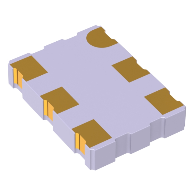
IDT8N0DV85
6-lead ceramic 5mm x 7mm x 1.55mm
package body
CD Package
Top View
©2012 Integrated Device Technology, Inc.
�IDT8N0DV85 Data Sheet
LVCMOS Dual-Frequency Programmable VCXO
Pin Description and Characteristic Tables
Table 1. Pin Descriptions
Number
Name
1
VC
Type
Input
Description
VCXO Control Voltage input.
PulldownNOTE 1
2
FSEL
Input
3
GND
Power
Power supply pin.
4
Q
Output
Clock output. LVCMOS interface levels.
5
DNU
6
VCC
Frequency select pin. See Table 3B for function. LVCMOS/LVTTL interface levels.
Do not use.
Power
Power supply pin.
NOTE 1.Pulldown refers to internal input resistors. See Table 2, Pin Characteristics, for typical values
Table 2. Pin Characteristics
Symbol
Parameter
Test Conditions
CIN
Input Capacitance
CPD
Power Dissipation Capacitance
RPULLDOWN
Input Pulldown Resistor
ROUT
Output Impedance
Minimum
Typical
Maximum
Units
FSEL
5.5
pF
VC
10
pF
8
pF
50
kΩ
VCC = 3.3V
14
Ω
VCC = 2.5V
17
Ω
Q
VCC = 3.465V or 2.625V
Function Tables
Table 3A. Output Frequency
15.476MHz to 260MHz
NOTE. Supported output frequency range. The output frequency can be programmed to any frequency in this range and to a precision of
218Hz.
IDT8N0DV85ACD REVISION A AUGUST 14, 2012
2
©2012 Integrated Device Technology, Inc.
�IDT8N0DV85 Data Sheet
LVCMOS Dual-Frequency Programmable VCXO
Principles of Operation
Frequency Configuration
The block diagram consists of the internal 3RD overtone crystal and
oscillator which provide the reference clock fXTAL of 114.285MHz.
The PLL includes the FemtoClock NG VCO along with the
Pre-divider (P), the feedback divider (M) and the post divider (N). The
P, M, and N dividers determine the output frequency based on the
fXTAL reference. The feedback divider is fractional supporting a huge
number of output frequencies. Internal registers are used to hold up
to two different factory pre-set configuration settings. The
configuration is selected via the FSEL pin. Changing the FSEL
control results in an immediate change of the output frequency to the
selected register values. The P, M, and N frequency configurations
support an output frequency range 15.476MHz to 260MHz.
An order code is assigned to each frequency configuration and the
VCXO pull-range programmed by the factory (default frequencies).
For more information on the available default frequencies and order
codes, please see the Ordering Information Section in this document.
For available order codes, see the FemtoClock NG Ceramic-Package
XO and VCXO Ordering Product Information document.
For more information on programming capabilities of the device for
custom frequency and pull-range configurations, see the FemtoClock
NG Ceramic 5x7 Module Programming Guide.
The devices use the fractional feedback divider with a delta-sigma
modulator for noise shaping and robust frequency synthesis
capability. The relatively high reference frequency minimizes phase
noise generated by frequency multiplication and allows more efficient
shaping of noise by the delta-sigma modulator. The output frequency
is determined by the 2-bit pre-divider (P), the feedback divider (M)
and the 7-bit post divider (N). The feedback divider (M) consists of
both a 7-bit integer portion (MINT) and an 18-bit fractional portion
(MFRAC) and provides the means for high-resolution frequency
generation. The output frequency fOUT is calculated by:
1
MFRAC + 0.5
f OUT = f XTAL ⋅ ------------ ⋅ MINT + ------------------------------------P⋅N
18
2
IDT8N0DV85ACD REVISION A AUGUST 14, 2012
Table 3B. Frequency Selection
Input
FSEL
Selects
0 (default)
Frequency 0
1
Frequency 1
(1)
3
©2012 Integrated Device Technology, Inc.
�IDT8N0DV85 Data Sheet
LVCMOS Dual-Frequency Programmable VCXO
Absolute Maximum Ratings
NOTE: Stresses beyond those listed under Absolute Maximum Ratings may cause permanent damage to the device. These ratings are stress
specifications only. Functional operation of product at these conditions or any conditions beyond those listed in the DC Characteristics or AC
Characteristics is not implied. Exposure to absolute maximum rating conditions for
extended periods may affect product reliability.
Item
Rating
Supply Voltage, VCC
3.63V
Inputs, VI
-0.5V to VCC + 0.5V
Outputs, VO
-0.5V to VCC + 0.5V
Package Thermal Impedance, θJA
49.4°C/W (0 mps)
Storage Temperature, TSTG
-65°C to 150°C
DC Electrical Characteristics
Table 4A. Power Supply DC Characteristics, VCC = 3.3V ± 5%, TA = -40°C to 85°C
Symbol
Parameter
VCC
Power Supply Voltage
ICC
Power Supply Current
Test Conditions
Minimum
Typical
Maximum
Units
3.135
3.3
3.465
V
135
163
mA
Minimum
Typical
Maximum
Units
2.375
2.5
2.625
V
124
148
mA
Table 4B. Power Supply DC Characteristics, VCC = 2.5V ± 5%, TA = -40°C to 85°C
Symbol
Parameter
VCC
Power Supply Voltage
ICC
Power Supply Current
Test Conditions
Table 4C. LVCMOS/LVTTL DC Characteristic, VCC = 3.3V ± 5% or VCC = 2.5V ± 5%, TA = -40°C to 85°C
Symbol
Parameter
VIH
Input High Voltage
VIL
Input Low Voltage
IIH
Input High Current
FSEL
VCC = VIN = 3.465V or 2.625V
IIL
Input Low Current
FSEL
VCC = 3.465V or 2.625V, VIN = 0V
-5
µA
VOH
Output High Voltage
Q
VCC = 3.465V
2.6
V
VCC = 2.625V
1.8
V
VOL
Output Low Voltage
Q
IDT8N0DV85ACD REVISION A AUGUST 14, 2012
Test Conditions
Minimum
VCC = 3.3V
Maximum
Units
2
VCC + 0.3
V
VCC = 2.5V
1.7
VCC + 0.3
V
VCC = VIN = 3.465V
-0.3
0.8
V
VCC = VIN = 2.5V
-0.3
0.7
V
150
µA
VCC = 3.465V or 2.625V
4
Typical
0.6
V
©2012 Integrated Device Technology, Inc.
�IDT8N0DV85 Data Sheet
LVCMOS Dual-Frequency Programmable VCXO
AC Electrical Characteristics
Table 5A. VCXO Control Voltage Input (VC) Characterisitics, VCC = 3.3V ± 5% or 2.5V ± 5%, TA = -40°C to 85°C
Symbol
Parameter
Oscillator Gain, NOTE 1, 2, 3
VCC = 3.3V
KV
Oscillator Gain, NOTE 1, 2, 3
VCC = 2.5V
LVC
Control Voltage Linearity
BW
Modulation Bandwidth
RVC
VC Input Resistance
VCNOM
Nominal Control Voltage
VC
Control Voltage Tuning
Range; NOTE 4
Test Conditions
Minimum
Typical
Maximum
Units
ADC_GAIN[5:0] = 000001
7.57
ppm/V
ADC_GAIN[5:0] = 000010
15.15
ppm/V
ADC_GAIN[5:0] = XXXXXX
25 · ADC_GAIN ÷ VCC
ppm/V
ADC_GAIN[5:0] = 111110
469.69
ppm/V
ADC_GAIN[5:0] = 111111
477.27
ppm/V
ADC_GAIN[5:0] = 000001
10
ppm/V
ADC_GAIN[5:0] = 000010
20
ppm/V
ADC_GAIN[5:0] = XXXXXX
25 · ADC_GAIN ÷ VCC
ppm/V
ADC_GAIN[5:0] = 111110
620
ppm/V
ADC_GAIN[5:0] = 111111
630
ppm/V
BSL Variation; NOTE 4
-1
±0.1
+1
100
kHz
500
kΩ
VCC÷2
0
%
V
VCC
V
NOTE: Electrical parameters are guaranteed over the specified ambient operating temperature range, which is established when the
device is mounted in a test socket with maintained transverse airflow greater than 500lfpm. The device will meet specifications after
thermal equilibrium has been reached under these conditions.
NOTE 1: VC = 10% to 90% of VCC.
NOTE 2: Nominal oscillator gain: Pull range divided by the control voltage tuning range of 3.3V.
E.g. for ADC_GAIN[6:0] = 000001 the pull range is ±12.5ppm, resulting in an oscillator gain of 25ppm ÷ 3.3V = 7.57ppm/V.
NOTE 3: For best phase noise performance, use the lowest KV that meets the requirements of the application.
NOTE 4: BSL = Best Straight Line Fit: Variation of the output frequency vs. control voltage VC, in percent. VC ranges from 10% to 90% VCC.
IDT8N0DV85ACD REVISION A AUGUST 14, 2012
5
©2012 Integrated Device Technology, Inc.
�IDT8N0DV85 Data Sheet
LVCMOS Dual-Frequency Programmable VCXO
Table 5B. AC Characterisitics, VCC = 3.3V ± 5% or 2.5V ± 5%, TA = -40°C to 85°C
Symbol
Parameter
fOUT
Output Frequency Q
fI
Initial Accuracy
fS
fA
fT
Temperature Stability
Test Conditions
Minimum
Typical
Maximum
Units
260
MHz
Measured at 25°C
±10
ppm
Option Code = A or B
±100
ppm
Option Code = E or F
±50
ppm
Option Code = K or L
±20
ppm
Frequency drift over 10 year life
±3
ppm
Frequency drift over 15 year life
±5
ppm
Option Code A or B (10 year life time)
±113
ppm
Option Code E or F (10 year life time)
±63
ppm
Option Code K or L (10 year life time)
±33
ppm
15.476
Aging
Total Stability
tjit(cc)
Cycle-to-Cycle Jitter NOTE 1, 2, 3
20
ps
tjit(per)
Period Jitter, RMS; NOTE 1, 2, 3
3.3
ps
tjit(Ø)
RMS Phase Jitter (Random)
NOTE 4
fOUT = 156.25MHz,
Integration Range: 12kHz - 20MHz
0.65
fOUT = 156.25MHz,
Integration Range: 1kHz - 40MHz
0.94
Integration Range: 12kHz - 20MHz
0.65
0.90
ps
ps
tjit(Ø)
RMS Phase Jitter (Random)
NOTE 4, 5
ΦN(100)
Single-side Band Phase Noise
fOUT = 156.25MHz, 100Hz from Carrier
-65
dBc/Hz
ΦN(1k)
Single-side band phase noise
fOUT = 156.25MHz, 1kHz from Carrier
-96
dBc/Hz
ΦN(10k)
Single-side band phase noise
fOUT = 156.25MHz, 10kHz from Carrier
-117
dBc/Hz
ΦN(100k)
Single-side band phase noise
fOUT = 156.25MHz, 100kHz from Carrier
-126
dBc/Hz
ΦN(1M)
Single-side band phase noise,
fOUT = 156.25MHz, 1MHz from Carrier
-138
dBc/Hz
ΦN(10M)
Single-side band phase noise,
fOUT = 156.25MHz, 10MHz from Carrier
-144
dBc/Hz
tR / tF
Output Rise/Fall Time
odc
Output Duty Cycle
tSTARTUP
tSET
20% to 80%
1.05
ps
175
715
ps
45
55
%
Device Start-up Time After Power-up
20
ms
Output Frequency Settling Time After
FSEL0 and FSEL1 Values are
Changed
1
ms
NOTE: Characterized with VC in linear range.
NOTE: XTAL parameters (Initial Accuracy, temperature Stability, Aging and Total Stability) are guaranteed by manufacturing.
NOTE: Electrical parameters are guaranteed over the specified ambient operating temperature range, which is established when the device is
mounted in a test socket with maintained transverse airflow greater than 500 lfpm. The device will meet specifications after thermal equilibrium
has been reached under these conditions.
NOTE 1: This parameter is defined in accordance with JEDEC standard 65.
NOTE 2: Tested at supply voltage VCC = 3.3V ± 5%.
NOTE 3: Applies to output frequencies: 15.476, 19.44, 25, 33.33, 74.174, 74.25, 100, 106.25, 122.88, 125, 150, 155.52, 156.25, 161.132,
176.8328, 187.5, 200, 212.5, 250 and 260MHz.
NOTE 4: Refer to phase noise plot.
NOTE 5: Applies to output frequencies: 25, 33.33, 100, 106.25, 122.88, 125, 148.5, 150, 155.52, 156.25, 161.132, 164.3555, 166.62875,
176.8328, 187.5, 212.5 and 250MHz.
IDT8N0DV85ACD REVISION A AUGUST 14, 2012
6
©2012 Integrated Device Technology, Inc.
�IDT8N0DV85 Data Sheet
LVCMOS Dual-Frequency Programmable VCXO
Noise Power
dBc
Hz
Typical Phase Noise at 156.25MHz (12kHz - 20MHz)
Offset Frequency (Hz)
IDT8N0DV85ACD REVISION A AUGUST 14, 2012
7
©2012 Integrated Device Technology, Inc.
�IDT8N0DV85 Data Sheet
LVCMOS Dual-Frequency Programmable VCXO
Parameter Measurement Information
1.25V+5%
1.65V+5%
SCOPE
VCC
SCOPE
VCC
Qx
Qx
GND
GND
1.25V+5%
1.65V+5%
3.3V LVCMOS/LVTTL Output Load AC Test Circuit
2.5V LVCMOS/LVTTL Output Load AC Test Circuit
Noise Power
Phase Noise Plot
80%
80%
Q
20%
20%
tR
f1
Offset Frequency
tF
f2
RMS Phase Jitter =
1
* Area Under Curve Defined by the Offset Frequency Markers
2* *ƒ
Output Rise and Fall Time
RMS Phase Jitter
VOH
V
CC
2
Q
VREF
t PW
t
odc =
t PW
VOL
1σ contains 68.26% of all measurements
2σ contains 95.4% of all measurements
3σ contains 99.73% of all measurements
4σ contains 99.99366% of all measurements
6σ contains (100-1.973x10⁻⁷)% of all measurements
PERIOD
x 100%
Reference Point
t PERIOD
(Trigger Edge)
Histogram
Mean Period
(First edge after trigger)
Output Duty Cycle/Pulse Width/Period
IDT8N0DV85ACD REVISION A AUGUST 14, 2012
RMS Period Jitter
8
©2012 Integrated Device Technology, Inc.
�IDT8N0DV85 Data Sheet
LVCMOS Dual-Frequency Programmable VCXO
Applications Information
Recommendations for Unused Input Pins
Inputs:
LVCMOS Pins
The control pin has an internal pulldown; additional resistance is not
required but can be added for additional protection. A 1kΩ resistor
can be used.
IDT8N0DV85ACD REVISION A AUGUST 14, 2012
9
©2012 Integrated Device Technology, Inc.
�IDT8N0DV85 Data Sheet
LVCMOS Dual-Frequency Programmable VCXO
Schematic Layout
Figure 1 shows an example of IDT8N0DV85 application schematic.
In this example, the device is operated at VCC = 3.3V. The schematic
example focuses on functional connections and is intended as an
example only and may not represent the exact user configuration.
Refer to the pin description and functional tables in the datasheet to
ensure the logic control inputs are properly set. For example FSEL
can be configured from an FPGA instead of set with pull up and pull
down resistors as shown.
As with any high speed analog circuitry, the power supply pins are
vulnerable to random noise, so to achieve optimum jitter performance
isolation of the VCC pin from the power supply is required. In order to
achieve the best possible filtering, it is recommended that the
placement of the filter components be on the device side of the PCB
as close to the power pins as possible. If space is limited, the 0.1µF
capacitor on the VCC pin must be placed on the device side with
direct return to the ground plane though vias. The remaining filter
components can be on the opposite side of the PCB.
The typical application of the IDT8N0DV85 is a voltage-controlled
oscillator as part of a PLL. The two connections necessary to be
made to the PLL are VC, the analog control voltage that sets the
center frequency of the VCXO, and Q, which is the oscillator output.
VC is the analog output of the PLL low pass loop filter that serves to
remove noise from the phase detector error output.
Power supply filter component recommendations are a general
guideline to be used for reducing external noise from coupling into
the devices. The filter performance is designed for a wide range of
noise frequencies. This low-pass filter starts to attenuate noise at
approximately 10kHz. If a specific frequency noise component is
known, such as switching power supplies frequencies, it is
recommended that component values be adjusted and if required,
additional filtering be added. Additionally, good general design
practices for power plane voltage stability suggests adding bulk
capacitance in the local area of all devices.
In order to achieve the best possible filtering, it is recommended that
the placement of the filter components be on the device side of the
PCB as close to the power pins as possible. If space is limited, the
0.1µF capacitor in each power pin filter should be placed on the
device side of the PCB and the other components can be placed on
the opposite side.
Logic Control Input Examples
Set Logic
Input to '1'
VCC
Set Logic
Input to '0'
VCC
3.3V
2
VCC
RU1
1K
RU2
Not Install
To Logic
Input
pins
RD1
Not Install
C2
FB1
1
BLM18BB221SN1
10uF
To Logic
Input
pins
C1
0.1uF
RD2
1K
Analog Control Voltage
is the low pass filtered
output of a PLL Phase
Detector.
Place 0.1uF bypass
cap directly
adjacent to the VCC
pin.
U1
1
Analog Control Voltage
FSEL
2
3
VC
VCC
FSEL DNU
GND
Q
6
VCC
C3
0.1uF
5
4
IDT8N0DV85CD
R3
Q
33
Q is connected to
the VCXO input
pin of a PLL.
Figure 1. IDT8N0DV85 Application Schematic
IDT8N0DV85ACD REVISION A AUGUST 14, 2012
10
©2012 Integrated Device Technology, Inc.
�IDT8N0DV85 Data Sheet
LVCMOS Dual-Frequency Programmable VCXO
Power Considerations
This section provides information on power dissipation and junction temperature for the IDT8N0DV85.
Equations and example calculations are also provided.
1.
Power Dissipation.
The total power dissipation for the IDT8N0DV85 is the sum of the core power plus the power dissipation in the load(s). The following is the
power dissipation for VCC = 3.3V +5% = 3.465V, which gives worst case results.
•
Power (core)MAX = VCC_MAX * ICC= 3.465V * 163mA = 564.8mW
Total Static Power:
= Power (core)MAX = 564.8mW
Dynamic Power Dissipation at FOUT (max)
Total Power (FOUT_MAX) = [(CPD * N) * Frequency * (VCC)2] = [(8pF *1) * 260MHz * (3.465V)2] = 25mW
Total Power
Total Power
= Static Power + Dynamic Power Dissipation
= 564.8mW + 25mW
= 589.8mW
2. Junction Temperature.
Junction temperature, Tj, is the temperature at the junction of the bond wire and bond pad, and directly affects the reliability of the device. The
maximum recommended junction temperature is 125°C. Limiting the internal transistor junction temperature, Tj, to 125°C ensures that the bond
wire and bond pad temperature remains below 125°C.
The equation for Tj is as follows: Tj = θJA * Pd_total + TA
Tj = Junction Temperature
θJA = Junction-to-Ambient Thermal Resistance
Pd_total = Total Device Power Dissipation (example calculation is in section 1 above)
TA = Ambient Temperature
In order to calculate junction temperature, the appropriate junction-to-ambient thermal resistance θJA must be used. Assuming no air flow and
a multi-layer board, the appropriate value is 49.4°C/W per Table 6 below.
Therefore, Tj for an ambient temperature of 85°C with all outputs switching is:
85°C + 0.590W * 49.4°C/W = 114.1°C. This is below the limit of 125°C.
This calculation is only an example. Tj will obviously vary depending on the number of loaded outputs, supply voltage, air flow and the type of
board (multi-layer).
Table 6. Thermal Resistance θJA for a 6-lead Ceramic 5mm x 7mm Package, Forced Convection
θJA by Velocity
Meters per Second
Multi-Layer PCB, JEDEC Standard Test Boards
IDT8N0DV85ACD REVISION A AUGUST 14, 2012
0
1
2
49.4°C/W
44.2°C/W
42.1°C/W
11
©2012 Integrated Device Technology, Inc.
�IDT8N0DV85 Data Sheet
LVCMOS Dual-Frequency Programmable VCXO
Reliability Information
Table 7. θJA vs. Air Flow Table for a 6-lead Ceramic 5mm x 7mm Package
θJA vs. Air Flow
Meters per Second
Multi-Layer PCB, JEDEC Standard Test Boards
0
1
2
49.4°C/W
44.2°C/W
42.1°C/W
Transistor Count
The transistor count for IDT8N0DV85 is: 47,414
IDT8N0DV85ACD REVISION A AUGUST 14, 2012
12
©2012 Integrated Device Technology, Inc.
�IDT8N0DV85 Data Sheet
LVCMOS Dual-Frequency Programmable VCXO
Package Outline and Package Dimensions
IDT8N0DV85ACD REVISION A AUGUST 14, 2012
13
©2012 Integrated Device Technology, Inc.
�IDT8N0DV85 Data Sheet
LVCMOS Dual-Frequency Programmable VCXO
Ordering Information for FemtoClock NG Ceramic-Package XO and VCXO Products
The programmable VCXO and XO devices support a variety of
devices options such as the output type, number of default frequencies, internal crystal frequency, power supply voltage, ambient
temperature range and the frequency accuracy. The device options,
default frequencies and default VCXO pull range must be specified at
the time of order and are programmed by IDT before the shipment.
The table below specifies the available order codes, including the
device options and default frequency configurations. Example part
number: the order code 8N3QV01FG-0001CDI specifies a
programmable, quad default-frequency VCXO with a voltage supply
of 2.5V, a LVPECL output, a ±50ppm crystal frequency accuracy,
contains a 114.285MHz internal crystal as frequency source,
industrial temperature range, a lead-free (6/6 RoHS) 6-lead ceramic
5mm x 7mm x 1.55mm package and is factory-programmed to the
default frequencies of 100MHz, 122.88MHz, 125MHz and
156.25MHz and to the VCXO pull range of min. ±100ppm.
Other default frequencies and order codes are available from IDT on
request. For more information on available default frequencies, see
the FemtoClock NG Ceramic-Package XO and VCXO Ordering
Product Information document.
Part/Order Numbers
8N X
X
XXX X X - dddd XX X
X
Shipping Package
8: Tape & Reel
(no letter): Tray
FemtoClock NG
Ambient Temperature Range
“I”: Industrial: (TA = -40°C to 85°C)
(no letter) : (TA = 0°C to 70°C)
I/O Identifier
0: LVCMOS
3: LVPECL
4: LVDS
Package Code
CD: Lead-Free, 6/10-lead ceramic 5mm x 7mm x 1.55mm
Number of Default Frequencies
S: 1: Single
D: 2: Dual
Q: 4: Quad
Part Number
Function
#pins
OE fct. at
pin
001
XO
10
OE@2
003
XO
10
OE@1
V01
VCXO
10
OE@2
V03
VCXO
10
OE@1
V75
VCXO
6
OE@2
V76
VCXO
6
nOE@2
V85
VCXO
6
—
085
XO
6
OE@1
270
XO
6
OE@1
271
XO
6
OE@2
272
XO
6
nOE@2
273
XO
6
nOE@1
Default-Frequency and VCXO Pull Range
See document FemtoClock NG Ceramic-Package XO and VCXO
Ordering Product Information.
dddd
fXTAL (MHz)
PLL feedback
Use for
0000 to 0999
114.285
Fractional
VCXO, XO
Integer
XO
Fractional
XO
1000 to 1999
2000 to 2999
100.000
Last digit = L: configuration pre-programmed and not
Die Revision
A
Option Code (Supply Voltage and Frequency-Stability)
A: VCC = 3.3V±5%, ±100ppm
B: VCC = 2.5V±5%, ±100ppm
E: VCC = 3.3V±5%, ±50ppm
F: VCC = 2.5V±5%, ±50ppm
K: VCC = 3.3V±5%, ±20ppm
L: VCC = 2.5V±5%, ±20ppm
NOTE: For order information, also see the FemtoClock NG Ceramic-Package XO and VCXO Ordering Product Information document.
IDT8N0DV85ACD REVISION A AUGUST 14, 2012
14
©2012 Integrated Device Technology, Inc.
�IDT8N0DV85 Data Sheet
LVCMOS Dual-Frequency Programmable VCXO
Table 8. Device Marking
Marking
Industrial Temperature Range (TA = -40°C to 85°C)
Commercial Temperature Range (TA = 0°C to 70°C)
IDT8N0DV85yAddddCDI
IDT8N0DV85yAddddCD
y = Option Code, dddd=Default-Frequency and VCXO Pull Range
IDT8N0DV85ACD REVISION A AUGUST 14, 2012
15
©2012 Integrated Device Technology, Inc.
�IDT8N0DV85 Data Sheet
LVCMOS Dual-Frequency Programmable VCXO
We’ve Got Your Timing Solution
6024 Silver Creek Valley Road
San Jose, California 95138
Sales
800-345-7015 (inside USA)
+408-284-8200 (outside USA)
Fax: 408-284-2775
www.IDT.com/go/contactIDT
Technical Support
netcom@idt.com
+480-763-2056
DISCLAIMER Integrated Device Technology, Inc. (IDT) and its subsidiaries reserve the right to modify the products and/or specifications described herein at any time and at IDT’s sole discretion. All information in this document,
including descriptions of product features and performance, is subject to change without notice. Performance specifications and the operating parameters of the described products are determined in the independent state and are not
guaranteed to perform the same way when installed in customer products. The information contained herein is provided without representation or warranty of any kind, whether express or implied, including, but not limited to, the
suitability of IDT’s products for any particular purpose, an implied warranty of merchantability, or non-infringement of the intellectual property rights of others. This document is presented only as a guide and does not convey any
license under intellectual property rights of IDT or any third parties.
IDT’s products are not intended for use in applications involving extreme environmental conditions or in life support systems or similar devices where the failure or malfunction of an IDT product can be reasonably expected to significantly affect the health or safety of users. Anyone using an IDT product in such a manner does so at their own risk, absent an express, written agreement by IDT.
Integrated Device Technology, IDT and the IDT logo are registered trademarks of IDT. Other trademarks and service marks used herein, including protected names, logos and designs, are the property of IDT or their respective third
party owners.
Copyright 2012. All rights reserved.
�