Quad-Frequency
Programmable VCXO
IDT8N0QV01 Rev H
DATASHEET
General Description
Features
The 8N0QV01 is a Quad-Frequency Programmable VCXO with very
flexible frequency and pull-range programming capabilities. The
device uses IDT’s Fourth Generation FemtoClock® NG technology
for an optimum of high clock frequency and low phase noise
performance. The device accepts 2.5V or 3.3V supply and is
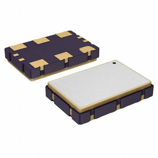
packaged in a small, lead-free (RoHS 6) 10-lead ceramic 5mm x
7mm x 1.55mm package.
•
•
Fourth generation FemtoClock® NG technology
•
Four power-up default frequencies (see part number order codes),
re-programmable by I2C
•
I2C programming interface for the output clock frequency, APR
and internal PLL control registers
•
•
Frequency programming resolution is 435.9Hz ÷N
•
•
•
•
One 2.5V, 3.3V LVCMOS clock output
Besides the four default power-up frequencies set by the FSEL0 and
FSEL1 pins, the 8N0QV01 can be programmed via the I2C interface
to any output clock frequency between 15.476MHz to 260MHz to a
very high degree of precision with a frequency step size of 435.9Hz
÷N (N: PLL post divider). Since the FSEL0 and FSEL1 pins are
mapped to four independent PLL, P, M and N divider registers (P,
MINT, MFRAC and N), reprogramming those registers to other
frequencies under control of FSEL0 and FSEL1 is supported. The
extended temperature range supports wireless infrastructure,
telecommunication and networking end equipment requirements.
Programmable clock output frequency from
15.476MHz to 260MHz
Absolute pull-range (APR) programmable from
±2.5 to ±727.5ppm
Two control inputs for the power-up default frequency
LVCMOS/LVTTL compatible control inputs
RMS phase jitter @ 156.25MHz
(12kHz - 20MHz): 0.635ps (typical)
•
RMS phase jitter @ 156.25MHz
(1kHz - 40MHz): 0.850ps (typical)
•
•
•
2.5V or 3.3V supply voltage modes
-40°C to 85°C ambient operating temperature
Lead-free (RoHS 6) packaging
÷P
OSC
FemtoClock® NG
VCO
1950-2600MHz
PFD
&
LPF
÷N
Q
VC
10
1
SDATA
Pin Assignment
SCLK
Block Diagram
9
8
VDD
6
Q
114.285 MHz
FSEL1
FSEL0
SCLK
SDATA
OE
Pulldown
Pulldown
7
7
25
Configuration Register (ROM)
(Frequency, APR, Polarity)
Pullup
Pullup
I2C Control
4
5
FSEL1
2
A/D
VC
3
FSEL0
GND
÷MINT, MFRAC
IDT8N0QV01 Rev H
10-lead ceramic 5mm x 7mm x 1.55mm
package body
CD Package
Top View
Pullup
IDT8N0QV01HCD REVISION A MARCH 13, 2014
1
©2013 Integrated Device Technology, Inc.
�IDT8N0QV01 Rev H Data Sheet
QUAD-FREQUENCY PROGRAMMABLE-VCXO
Block Diagram with Programming Registers
÷P
OSC
Output Divider N
FemtoClock® NG
VCO
1950-2600MHz
PFD
&
LPF
÷N
114.285MHz
2
Feedback Divider M (25 Bit)
MINT
(7 bits)
7
MFRAC
(18 bits)
A/D
VC
7
18
7
34
Programming Registers
I2C Control
7
ADC_GAIN
ADC_POL
I2C:
6 bits
1 bit
Def:
6 bits
1 bit
P0
30
30
SCLK
SDATA
Pullup
Pullup
30
30
FSEL[1:0]
OE
MINT0
MFRAC0
41
7
N0
I2C:
2 bits
7 bits
18 bits
7 bits
Def:
2 bits
7 bits
18 bits
7 bits
P1
MINT1
MFRAC1
N1
I2C:
2 bits
7 bits
18 bits
7 bits
Def:
2 bits
7 bits
18 bits
7 bits
P2
MINT2
MFRAC2
N2
I2C:
2 bits
7 bits
18 bits
7 bits
Def:
2 bits
7 bits
18 bits
7 bits
P3
MINT3
MFRAC3
N3
I2C:
2 bits
7 bits
18 bits
7 bits
Def:
2 bits
7 bits
18 bits
7 bits
00
34
01
34
34
10
34
11
34
Pulldown, Pulldown
Pullup
Def: Power-up default register setting for I2C registers
ADC_GAINn, ADC_POL, Pn, MINTn, MFRACn and Nn
IDT8N0QV01HCD REVISION A MARCH 13, 2014
2
©2013 Integrated Device Technology, Inc.
�IDT8N0QV01 Rev H Data Sheet
QUAD-FREQUENCY PROGRAMMABLE-VCXO
Pin Description and Characteristics
Table 1. Pin Descriptions
Number
Name
Type
Description
1
VC
Input
2
OE
Input
3
GND
Power
5, 4
FSEL1,
FSEL0
Input
6
Q
Output
7
DNU
8
VDD
Power
9
SDATA
Input
Pullup
I2C Data Input. LVCMOS/LVTTL interface levels.
10
SCLK
Input
Pullup
I2C Clock Input. LVCMOS/LVTTL interface levels.
VCXO Control Voltage. The control voltage versus frequency
characteristics are set by the ADC_GAIN[5:0] register bits.
Output enable pin. See Table 3B for function. LVCMOS/LVTTL interface
levels.
Pullup
Power supply ground.
Pulldown
Default frequency select pins. LVCMOS/LVTTL interface levels. Refer to
the FemtoClock NG Ceramic-Package XO and VCXO Ordering Product
Information document for default frequency order codes.
Clock output. LVCMOS/LVTTL interface levels.
Do not use. Do not connect.
Positive power supply.
NOTE: Pullup and Pulldown refer to internal input resistors. See Table 2, Pin Characteristics, for typical values.
Table 2. Pin Characteristics
Symbol
Parameter
CIN
Input Capacitance
CPD
Power Dissipation
Capacitance
RPULLUP
Test Conditions
Minimum
Typical
Maximum
Units
FSEL[1:0], SDATA, SCLK, OE
3.5
pF
VC
10
pF
VDD = 3.465V or 2.625V
8
pF
Input Pullup Resistor
50
k
RPULLDOWN
Input Pulldown Resistor
50
k
Output Impedance
VDD = 3.3V
15
ROUT
VDD = 2.5V
19
Q
IDT8N0QV01HCD REVISION A MARCH 13, 2014
3
©2013 Integrated Device Technology, Inc.
�IDT8N0QV01 Rev H Data Sheet
QUAD-FREQUENCY PROGRAMMABLE-VCXO
Function Tables
Table 3A. Default Frequency Selection
Input
FSEL1
FSEL0
Operation
0 (default)
0 (default)
Default frequency 0.
0
1
Default frequency 1.
1
0
Default frequency 2.
1
1
Default frequency 3.
NOTE: The default frequency is the output frequency after power-up. One of four default frequencies is selected by FSEL[1:0]. See
programming section for details.
Table 3B. OE Configuration
Input
OE
0
1 (default)
Output Enable
Output Q are in high-impedance state.
Outputs are enabled.
NOTE: OE is an asynchronous control.
IDT8N0QV01HCD REVISION A MARCH 13, 2014
4
©2013 Integrated Device Technology, Inc.
�IDT8N0QV01 Rev H Data Sheet
QUAD-FREQUENCY PROGRAMMABLE-VCXO
Principles of Operation
The four configuration registers for the P, M (MINT & MFRAC) and N
dividers which are named Pn, MINTn, MFRACn and Nn with n = 0 to
3. “n” denominates one of the four possible configurations.
The block diagram consists of the internal 3rd overtone crystal and
oscillator which provide the reference clock fXTAL of 114.285MHz.
The PLL includes the FemtoClock NG VCO along with the pre-divider
(P), the feedback divider (M) and the post divider (N). The P, M, and
N dividers determine the output frequency based on the fXTAL
reference and must be configured correctly for proper operation. The
feedback divider is fractional supporting a huge number of output
frequencies. The configuration of the feedback divider to integer-only
values results in an improved output phase noise characteristics at
the expense of the range of output frequencies. In addition, internal
registers are used to hold up to four different factory pre-set P, M, and
N configuration settings. These default pre-sets are stored in the I2C
registers at power-up. Each configuration is selected via the
FSEL[1:0] pins and can be read back using the SCLK and SDATA
pins.
As identified previously, the configurations of P, M (MINT & MFRAC)
and N divider settings are stored the I2C register, and the
configuration loaded at power-up is determined by the FSEL[1:0]
pins.
Table 4. Frequency Selection
Input
The user may choose to operate the device at an output frequency
different than that set by the factory. After power-up, the user may
write new P, N and M settings into one or more of the four
configuration registers and then use the FSEL[1:0] pins to select the
newly programmed configuration. Note that the I2C registers are
volatile and a power supply cycle will reload the pre-set factory
default conditions.
FSEL1
FSEL0
Selects
Register
0 (def.)
0 (def.)
Frequency 0
P0, MINT0, MFRAC0, N0
0
1
Frequency 1
P1, MINT1, MFRAC1, N1
1
0
Frequency 2
P2, MINT2, MFRAC2, N2
1
1
Frequency 3
P3, MINT3, MFRAC3, N3
Frequency Configuration
An order code is assigned to each frequency and VCXO pull range
configuration programmed by the factory (default frequencies). For
available order codes, see the FemtoClock NG Ceramic-Package XO
and VCXO Ordering Product Information document.
If the user does choose to write a different P, M, and N configuration,
it is recommended to write to a configuration which is not currently
selected by FSEL[1:0] and then change to that configuration after the
I2C transaction has completed. Changing the FSEL[1:0] controls
results in an immediate change of the output frequency to the
selected register values. The P, M, and N frequency configurations
support an output frequency range 15.476MHz to 260MHz.
For more information and guidelines on programming of the device
for custom frequency configurations, programming for a specific
VCXO pull range, the available APR (absolute pull range), the
register description and the serial interface description, see the
FemtoClock NG Ceramic 5x7 Module Programming Guide.
The devices use the fractional feedback divider with a delta-sigma
modulator for noise shaping and robust frequency synthesis
capability. The relatively high reference frequency minimizes phase
noise generated by frequency multiplication and allows more efficient
shaping of noise by the delta-sigma modulator.
The output frequency is determined by the 2-bit pre-divider (P), the
feedback divider (M) and the 7-bit post divider (N). The feedback
divider (M) consists of both a 7-bit integer portion (MINT) and an
18-bit fractional portion (MFRAC) and provides the means for
high-resolution frequency generation. The output frequency fOUT is
calculated by:
1
MFRAC + 0.5
f OUT = f XTAL ------------- MINT + ------------------------------------PN
18
2
IDT8N0QV01HCD REVISION A MARCH 13, 2014
(1)
5
©2013 Integrated Device Technology, Inc.
�IDT8N0QV01 Rev H Data Sheet
QUAD-FREQUENCY PROGRAMMABLE-VCXO
Absolute Maximum Ratings
NOTE: Stresses beyond those listed under Absolute Maximum Ratings may cause permanent damage to the device. These ratings are stress
specifications only. Functional operation of the product at these conditions or any conditions beyond those listed in the DC Characteristics or
AC Characteristics is not implied. Exposure to absolute maximum rating conditions for extended periods may affect product reliability.
Item
Rating
Supply Voltage, VDD
3.6V
Inputs, VI
-0.5V to VDD + 0.5V
Outputs, IO (LVCMOS)
-0.5V to VDD + 0.5V
Outputs, IO (SDATA)
10mA
Package Thermal Impedance, JA
49.4°C/W (mps)
Storage Temperature, TSTG
-65°C to 150°C
DC Electrical Characteristics
Table 5A. Power Supply DC Characteristics, VDD = 3.3V ± 5%, TA = -40°C to 85°C
Symbol
Parameter
VDD
Supply Voltage
IDD
Power Supply Current
Test Conditions
Minimum
Typical
Maximum
Units
3.135
3.3
3.465
V
135
150
mA
Minimum
Typical
Maximum
Units
2.375
2.5
2.625
V
130
145
mA
No Load, OE = Low
Table 5B. Power Supply DC Characteristics, VDD = 2.5V ± 5%, TA = -40°C to 85°C
Symbol
Parameter
VDD
Supply Voltage
IDD
Power Supply Current
IDT8N0QV01HCD REVISION A MARCH 13, 2014
Test Conditions
No Load, OE = Low
6
©2013 Integrated Device Technology, Inc.
�IDT8N0QV01 Rev H Data Sheet
QUAD-FREQUENCY PROGRAMMABLE-VCXO
Table 5C. LVCMOS/LVTTL DC Characteristic, VDD = 3.3V ± 5% or 2.5V ± 5%, TA = -40°C to 85°C
Symbol
Parameter
VIH
Input High
Voltage
VIL
Input Low
Voltage
IIH
Input High
Current
IIL
Input Low
Current
Test Conditions
Minimum
OE, SCLK,
SDATA,
FSEL[1:0]
VDD = 3.3V
OE, SCLK,
SDATA,
FSEL[1:0]
Typical
Maximum
Units
2
VDD+ 0.3
V
VDD = 2.5V
1.7
VDD + 0.3
V
VDD = 3.465V
-0.3
0.8
V
VDD = 2.5V
-0.3
0.7
V
OE,
VDD = VIN = 3.465V or 2.625V
10
µA
SDATA, SCLK
VDD = VIN = 3.465V or 2.625V
5
µA
FSEL0, FSEL1
VDD = VIN = 3.465V or 2.625V
150
µA
OE
VDD = 3.465V or 2.625V,
VIN = 0V
-500
µA
SDATA, SCLK
VDD = 3.465V or 2.625V,
VIN = 0V
-150
µA
FSEL0, FSEL1
VDD = 3.465V or 2.625V,
VIN = 0V
-5
µA
VDD = 3.465V
2.4
V
VDD = 2.625
1.7
V
VOH
Output
High
Voltage
Q
VOL
Output Low
Voltage
Q
IDT8N0QV01HCD REVISION A MARCH 13, 2014
VDD = 3.6V or 2.625
7
0.4
V
©2013 Integrated Device Technology, Inc.
�IDT8N0QV01 Rev H Data Sheet
QUAD-FREQUENCY PROGRAMMABLE-VCXO
AC Electrical Characteristics
Table 6A. AC Characteristics, VDD = 3.3V ± 5% or 2.5V ± 5%, TA = -40°C to 85°C
Symbol
Parameter
fOUT
Output Frequency Q, nQ
fI
Initial Accuracy
fS
fA
fT
Temperature Stability
Aging
Total Stability
Test Conditions
Minimum
P = 1, N = 10...126
15.476
Typical
Cycle-to-Cycle Jitter; NOTE 1
tjit(per)
Period Jitter; NOTE 1
tjit(Ø)
RMS Phase Jitter (Random)
Units
260
MHz
Measured at 25°C at Final Test
±10
ppm
Option code = A or B
±100
ppm
Option code = E or F
±50
ppm
Option code = K or L
±20
ppm
Frequency drift over 10 year life
±3
ppm
Frequency drift over 15 year life
±5
ppm
Option code A or B (10 year life)
±113
ppm
Option code E or F (10 year life)
±63
ppm
Option code K or L (10 year life)
tjit(cc)
Maximum
±33
ppm
VDD = 3.3V
15
32
ps
VDD = 2.5V
18
40
ps
VDD = 3.3V
2.6
5
ps
VDD = 2.5V
4
7
ps
17MHz fout 260MHz, Integration
Range: 12kHz - 20MHz, NOTE 3
0.70
1.20
ps
156.25MHz, Integration Range:
12kHz - 20MHz; NOTE 2
0.64
0.92
ps
156.25MHz, Integration Range:
1kHz - 40MHz
0.85
1.00
ps
N(100)
Single-side band phase noise,
100Hz from Carrier
156.25MHz
-75
dBc/Hz
N(1k)
Single-side band phase noise,
1kHz from Carrier
156.25MHz
-98
dBc/Hz
N(10k)
Single-side band phase noise,
10kHz from Carrier
156.25MHz
-118
dBc/Hz
N(100k)
Single-side band phase noise,
100kHz from Carrier
156.25MHz
-127
dBc/Hz
N(1M)
Single-side band phase noise,
1MHz from Carrier
156.25MHz
-139
dBc/Hz
N(10M)
Single-side band phase noise,
10MHz from Carrier
156.25MHz
-143
dBc/Hz
tR / tF
Output Rise/Fall Time
odc
Output Duty Cycle
tOSC
tSET
VDD = 3.3V, 20% to 80%
150
425
700
ps
VDD = 2.5V, 20% to 80%
150
500
800
ps
45
50
55
%
Oscillator Start-Up Time
20
ms
Output frequency settling time after
FSEL0 and FSEL1 values are
changed
1
ms
NOTE: Electrical parameters are guaranteed over the specified ambient operating temperature range, which is established when the device is
mounted in a test socket with maintained transverse airflow greater than 500 lfpm. The device will meet specifications after thermal equilibrium
has been reached under these conditions.
NOTE: All AC parameters are characterized with P = 1.
NOTES continued on next page.
IDT8N0QV01HCD REVISION A MARCH 13, 2014
8
©2013 Integrated Device Technology, Inc.
�IDT8N0QV01 Rev H Data Sheet
QUAD-FREQUENCY PROGRAMMABLE-VCXO
NOTE: Please see the FemtoClock Ceramic 5x7 Modules Programming Guide for more information on PLL feedback modes and the optimum
configuration for phase noise.
NOTE 1: This parameter is defined in accordance with JEDEC standard 65.
NOTE 2: Please refer to the phase noise plots.
NOTE 3: Applies to output frequencies: 17MHz, 19.44MHz, 25MHz, 33.33MHz, 75MHz, 77.76MHz, 100MHz, 106.25MHz, 122.88MHz,
125MHz, 150MHz, 155.52MHz, 156.25MHz, 161.132MHz, 175MHz, 187.5MHz, 200MHz, 212.5MHz, 250MHz and 260MHz.
Table 6B. VCXO Control Voltage Input (VC) Characterisitics,
Symbol
Parameter
Test Conditions
Minimum
VDD = 3.3V
Maximum
Units
KV
Oscillator Gain, NOTE 1, 2, 3
7.57
477.27
ppm/V
VDD = 2.5V
10
630
ppm/V
LVC
Control Voltage Linearity; NOTE 4
BW
Modulation Bandwidth
BSL Variation
-5
100
kHz
ZVC
VC Input Impedance
500
k
VCNOM
Nominal Control Voltage
VDD/2
V
VC
Control Voltage Tuning Range;
NOTE 4
VDD = 3.3V ± 5% or 2.5V ± 5%,
TA = -40°C to 85°C
0
Typical
±0.4
+5
VDD
%
V
NOTE 1: VC = 0V to VDD. Oscillator gain is programmed by IDT. Gain = (25 · n) ÷ VCC and is in the range of n=1 to n = 63.
NOTE 2: Nominal oscillator gain: Please refer to the FemtoClock NG Ceramic 5x7 Module Programming Guide document.
NOTE 3: For best phase noise performance, use the lowest KV that meets the requirements of the application.
NOTE 4: BSL = Best Straight Line Fit: Variation of the output frequency vs. control voltage VC, in percent. VC ranges from 10% to 90% VDD.
IDT8N0QV01HCD REVISION A MARCH 13, 2014
9
©2013 Integrated Device Technology, Inc.
�IDT8N0QV01 Rev H Data Sheet
QUAD-FREQUENCY PROGRAMMABLE-VCXO
Noise Power (dBc/Hz)
Typical Phase Noise at 156.25MHz (12kHz - 20MHz)
Offset Frequency (Hz)
IDT8N0QV01HCD REVISION A MARCH 13, 2014
10
©2013 Integrated Device Technology, Inc.
�IDT8N0QV01 Rev H Data Sheet
QUAD-FREQUENCY PROGRAMMABLE-VCXO
Parameter Measurement Information
1.65V±5%
1.25V±5%
SCOPE
VDD
LVCMOS
SCOPE
VDD
Q
Q
LVCMOS
GND
GND
-1.25V±5%
-1.65V±5%
3.3V LVCMOS Output Load Test Circuit
2.5V LVCMOS Output Load Test Circuit
80%
80%
20%
20%
Q
RMS Phase Jitter
tR
tF
Output Rise/Fall Time
Q
Q
➤
tcycle n
➤
tcycle n+1
➤
➤
tjit(cc) = tcycle n tcycle n+1
1000 Cycles
Output Duty Cycle/Pulse Width/Period
IDT8N0QV01HCD REVISION A MARCH 13, 2014
Cycle-to-Cycle Jitter
11
©2013 Integrated Device Technology, Inc.
�IDT8N0QV01 Rev H Data Sheet
QUAD-FREQUENCY PROGRAMMABLE-VCXO
Parameter Measurement Information, continued
VOH
VREF
VOL
1σ contains 68.26% of all measurements
2σ contains 95.4% of all measurements
3σ contains 99.73% of all measurements
4σ contains 99.99366% of all measurements
6σ contains (100-1.973x10⁻⁷)% of all measurements
Reference Point
(Trigger Edge)
Histogram
Mean Period
(First edge after trigger)
Period Jitter
Applications Information
Recommendations for Unused Input Pins
Inputs:
LVCMOS Select Pins
All control pins have internal pullups or pulldowns; additional
resistance is not required but can be added for additional protection.
A 1k resistor can be used.
IDT8N0QV01HCD REVISION A MARCH 13, 2014
12
©2013 Integrated Device Technology, Inc.
�IDT8N0QV01 Rev H Data Sheet
QUAD-FREQUENCY PROGRAMMABLE-VCXO
Schematic Example
achieve the best possible filtering, it is recommended that the
placement of the filter components be on the device side of the PCB
as close to the power pins as possible. If space is limited, the 0.1µF
capacitor on the VDD pin must be placed on the device side with
direct return to the ground plane though vias. The remaining filter
components can be on the opposite side of the PCB.
Figure 1 shows an example 8N0QV01application schematic in which
the device is operated at VDD = +3.3V. The schematic example
focuses on functional connections and is intended as an example
only and may not represent the exact user configuration. Refer to the
pin description and functional tables in the datasheet to ensure the
logic control inputs are properly set. For example OE and FSEL[1:0]
can be configured from an FPGA instead of set with pull up and pull
down resistors as shown.
Power supply filter component recommendations are a general
guideline to be used for reducing external noise from coupling into
the devices. The filter performance is designed for a wide range of
noise frequencies. This low-pass filter starts to attenuate noise at
approximately 10kHz. If a specific frequency noise component is
known, such as switching power supplies frequencies, it is
recommended that component values be adjusted and if required,
additional filtering be added. Additionally, good general design
practices for power plane voltage stability suggests adding bulk
capacitance in the local area of all devices.
The 8N0QV01 is not a self contained part; it requires pairing with a
PLL. The two connections necessary to be made to the PLL are VC,
the analog control voltage that sets the center frequency of the
VCXO, and Q, which is the oscillator output. VC is the analog output
of the PLL low pass loop filter that serves to remove noise from the
phase detector error output.
As with any high speed analog circuitry, the power supply pins are
vulnerable to random noise, so to achieve optimum jitter performance
isolation of the VDD pin from the power supply is required. In order to
Figure 1. IDT8N0QV01 Schematic Example
IDT8N0QV01HCD REVISION A MARCH 13, 2014
13
©2013 Integrated Device Technology, Inc.
�IDT8N0QV01 Rev H Data Sheet
QUAD-FREQUENCY PROGRAMMABLE-VCXO
Power Considerations
This section provides information on power dissipation and junction temperature for the IDT8N0QV01.
Equations and example calculations are also provided.
1.
Power Dissipation.
The total power dissipation for the IDT8N0QV01 is the sum of the core power plus the power dissipation in the load(s). The following is the
power dissipation for VDD = 3.3V +5% = 3.465V, which gives worst case results.
•
Power (core)MAX = VDD_MAX * IDD = 3.465V * 150mA = 519.8mW
Total Static Power:
= Power (core)MAX = 519.8mW
Dynamic Power Dissipation at FOUT (max)
Total Power (FOUT_MAX) = [(CPD * N) * Frequency * (VDD)2] = [(8pF *1) * 260MHz * (3.465V)2] = 24.97mW
Total Power
= Static Power + Dynamic Power Dissipation
= 519.8mW + 24.97mW
= 544.77mW
2. Junction Temperature.
Junction temperature, Tj, is the temperature at the junction of the bond wire and bond pad, and directly affects the reliability of the device. The
maximum recommended junction temperature is 125°C. Limiting the internal transistor junction temperature, Tj, to 125°C ensures that the bond
wire and bond pad temperature remains below 125°C.
The equation for Tj is as follows: Tj = JA * Pd_total + TA
Tj = Junction Temperature
JA = Junction-to-Ambient Thermal Resistance
Pd_total = Total Device Power Dissipation (example calculation is in section 1 above)
TA = Ambient Temperature
In order to calculate junction temperature, the appropriate junction-to-ambient thermal resistance JA must be used. Assuming no air flow and
a multi-layer board, the appropriate value is 49.4°C/W per Table 7 below.
Therefore, Tj for an ambient temperature of 85°C with all outputs switching is:
85°C + 0.545W *49.4°C/W = 112°C. This is below the limit of 125°C.
This calculation is only an example. Tj will obviously vary depending on the number of loaded outputs, supply voltage, air flow and the type of
board (multi-layer).
Table 7. Thermal Resistance JA for a 10-lead Ceramic 5mm x 7mm Package, Forced Convection
JA by Velocity
Meters per Second
Multi-Layer PCB, JEDEC Standard Test Boards
IDT8N0QV01HCD REVISION A MARCH 13, 2014
0
1
2.5
49.4°C/W
44.2°C/W
41.0°C/W
14
©2013 Integrated Device Technology, Inc.
�IDT8N0QV01 Rev H Data Sheet
QUAD-FREQUENCY PROGRAMMABLE-VCXO
Reliability Information
Table 8. JA vs. Air Flow Table for a 10-lead Ceramic 5mm x 7mm Package
JA vs. Air Flow
Meters per Second
Multi-Layer PCB, JEDEC Standard Test Boards
0
1
2.5
49.4°C/W
44.2°C/W
41.0°C/W
Transistor Count
The transistor count for IDT8N0QV01 is: 47,302
IDT8N0QV01HCD REVISION A MARCH 13, 2014
15
©2013 Integrated Device Technology, Inc.
�IDT8N0QV01 Rev H Data Sheet
QUAD-FREQUENCY PROGRAMMABLE-VCXO
Package Outline and Package Dimensions
IDT8N0QV01HCD REVISION A MARCH 13, 2014
16
©2013 Integrated Device Technology, Inc.
�IDT8N0QV01 Rev H Data Sheet
QUAD-FREQUENCY PROGRAMMABLE-VCXO
Table 9. Device Marking
Industrial Temperature Range (TA = -40°C to 85°C)
Marking
IDT8N0QV01yHddddCDI
Commercial Temperature Range (TA = 0°C to 70°C)
IDT8N0QV01yHddddCD
y = Option Code, dddd=Default-Frequency and VCXO Pull Range
NOTE: For available order codes, see the FemtoClock NG Ceramic-Package XO and VCXO Ordering Product Information document.
For more information and guidelines on programming of the device for custom frequency configurations, programming for a specific VCXO pull
range, the available APR (absolute pull range), the register description and the serial interface description, see the FemtoClock NG
Ceramic 5x7 Module Programming Guide.
IDT8N0QV01HCD REVISION A MARCH 13, 2014
17
©2013 Integrated Device Technology, Inc.
�IDT8N0QV01 Rev H Data Sheet
QUAD-FREQUENCY PROGRAMMABLE-VCXO
Revision History Sheet
Rev
A
Table
Page
T1
3
6A
6B
8
9
14
Description of Change
Date
first row: deleted '(see Table 3C).'
forth row: replaced description.
Deleted NOTE 2 from RMS Phase Jitter. Added 'NOTE 2' to 156.25MHz.
Note 2: Added 'Please refer to the FemtoClock NG Ceramic 5x7 Module Programming
Guide document.'
Power Considerations. Changed Dynamic Power Dissipation from 2.5mW to 24.97mW
IDT8N0QV01HCD REVISION A MARCH 13, 2014
18
3/14/2014
©2013 Integrated Device Technology, Inc.
�IDT8N0QV01 Rev H Data Sheet
QUAD-FREQUENCY PROGRAMMABLE-VCXO
We’ve Got Your Timing Solution
6024 Silver Creek Valley Road
San Jose, California 95138
Sales
800-345-7015 (inside USA)
+408-284-8200 (outside USA)
Fax: 408-284-2775
www.IDT.com/go/contactIDT
Technical Support Sales
netcom@idt.com
+480-763-2056
DISCLAIMER Integrated Device Technology, Inc. (IDT) and its subsidiaries reserve the right to modify the products and/or specifications described herein at any time and at IDT’s sole discretion. All information in this document,
including descriptions of product features and performance, is subject to change without notice. Performance specifications and the operating parameters of the described products are determined in the independent state and are not
guaranteed to perform the same way when installed in customer products. The information contained herein is provided without representation or warranty of any kind, whether express or implied, including, but not limited to, the
suitability of IDT’s products for any particular purpose, an implied warranty of merchantability, or non-infringement of the intellectual property rights of others. This document is presented only as a guide and does not convey any
license under intellectual property rights of IDT or any third parties.
IDT’s products are not intended for use in applications involving extreme environmental conditions or in life support systems or similar devices where the failure or malfunction of an IDT product can be reasonably expected to significantly affect the health or safety of users. Anyone using an IDT product in such a manner does so at their own risk, absent an express, written agreement by IDT.
Integrated Device Technology, IDT and the IDT logo are registered trademarks of IDT. Other trademarks and service marks used herein, including protected names, logos and designs, are the property of IDT or their respective third
party owners.
Copyright 2013. All rights reserved.
�IMPORTANT NOTICE AND DISCLAIMER
RENESAS ELECTRONICS CORPORATION AND ITS SUBSIDIARIES (“RENESAS”) PROVIDES TECHNICAL
SPECIFICATIONS AND RELIABILITY DATA (INCLUDING DATASHEETS), DESIGN RESOURCES (INCLUDING
REFERENCE DESIGNS), APPLICATION OR OTHER DESIGN ADVICE, WEB TOOLS, SAFETY INFORMATION, AND
OTHER RESOURCES “AS IS” AND WITH ALL FAULTS, AND DISCLAIMS ALL WARRANTIES, EXPRESS OR IMPLIED,
INCLUDING, WITHOUT LIMITATION, ANY IMPLIED WARRANTIES OF MERCHANTABILITY, FITNESS FOR A
PARTICULAR PURPOSE, OR NON-INFRINGEMENT OF THIRD PARTY INTELLECTUAL PROPERTY RIGHTS.
These resources are intended for developers skilled in the art designing with Renesas products. You are solely responsible
for (1) selecting the appropriate products for your application, (2) designing, validating, and testing your application, and (3)
ensuring your application meets applicable standards, and any other safety, security, or other requirements. These
resources are subject to change without notice. Renesas grants you permission to use these resources only for
development of an application that uses Renesas products. Other reproduction or use of these resources is strictly
prohibited. No license is granted to any other Renesas intellectual property or to any third party intellectual property.
Renesas disclaims responsibility for, and you will fully indemnify Renesas and its representatives against, any claims,
damages, costs, losses, or liabilities arising out of your use of these resources. Renesas' products are provided only subject
to Renesas' Terms and Conditions of Sale or other applicable terms agreed to in writing. No use of any Renesas resources
expands or otherwise alters any applicable warranties or warranty disclaimers for these products.
(Rev.1.0 Mar 2020)
Corporate Headquarters
Contact Information
TOYOSU FORESIA, 3-2-24 Toyosu,
Koto-ku, Tokyo 135-0061, Japan
www.renesas.com
For further information on a product, technology, the most
up-to-date version of a document, or your nearest sales
office, please visit:
www.renesas.com/contact/
Trademarks
Renesas and the Renesas logo are trademarks of Renesas
Electronics Corporation. All trademarks and registered
trademarks are the property of their respective owners.
© 2020 Renesas Electronics Corporation. All rights reserved.
�