LVPECL Dual-Frequency
Programmable VCXO
IDT8N3DV85
DATASHEET
General Description
Features
The IDT8N3DV85 is a LVPECL Dual-Frequency Programmable
VCXO with very flexible frequency and pull-range programming
capabilities. The device uses IDT’s fourth generation FemtoClock®
NG technology for an optimum of high clock frequency and low
phase noise performance. The device accepts 2.5V or 3.3V supply
and is packaged in a small, lead-free (RoHS 6) 6-lead ceramic 5mm
x 7mm x 1.55mm package.
•
Fourth Generation FemtoClock® NG technology
•
Programmable clock output frequency from 15.476MHz to
866.67MHz and from 975MHz to 1,300MHz
•
•
•
Two factory-programmed output frequencies
•
•
•
VCXO pull range programmable from typical ±12.5 to ±787.5ppm
•
•
•
•
•
RMS phase jitter @ 622.08MHz (12kHz - 20MHz):0.46ps (typical)
The device can be factory-programmed to any two frequencies in the
range of 15.476MHz to 866.67MHz and from 975MHz to 1,300MHz
to the very high degree of frequency precision of 218Hz or better.
The output frequency is selected by the FSEL pin. The extended
temperature range supports wireless infrastructure, telecommunication and networking end equipment requirements.
VCO frequency programming resolution is 218Hz and better
Factory-programmable VCXO pull range and control voltage
polarity
One 2.5V or 3.3V LVPECL clock output
FSEL control input for frequency selection, LVCMOS/LVTTL
compatible
RMS phase jitter @ 622.08MHz (50kHz - 80MHz): 0.47ps (typical)
2.5V or 3.3V supply voltage
-40°C to 85°C ambient operating temperature
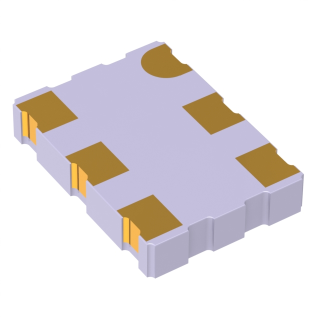
Lead-free (RoHS 6) 6-lead ceramic 5mm x 7mm x 1.55mm
package
Block Diagram
Pin Assignment
PFD
&
LPF
÷P
OSC
FemtoClock® NG
VCO
1950-2600MHz
Q
nQ
÷N
114.285 MHz
2
A/D
VC
FSEL
Pulldown
÷MINT, MFRAC
9
7
23
VC
1
6
VCC
FSEL
2
5
nQ
VEE
3
4
Q
IDT8N3DV85
6-lead ceramic 5mm x 7mm x 1.55mm
package body
CD Package
Top View
Configuration Register (ROM)
(Frequency, Pull range, Polarity)
IDT8N3DV85CCD REVISION A OCTOBER 30, 2013
1
©2013 Integrated Device Technology, Inc.
�IDT8N3DV85 Data Sheet
LVPECL DUAL-FREQUENCY PROGRAMMABLE VCXO
Pin Description and Characteristic Tables
Table 1. Pin Descriptions
Number
Name
Type
Description
1
VC
Input
2
FSEL
Input
3
VEE
Power
Negative power supply.
4, 5
Q, nQ
Output
Differential clock output. LVPECL interface levels.
6
VCC
Power
Positive power supply.
VCXO Control Voltage input.
Pulldown
Frequency select pin. See Table 3A for function. LVCMOS/LVTTL
interface levels.
NOTE: Pulldown refers to internal input resistors. See Table 2, Pin Characteristics, for typical values.
Table 2. Pin Characteristics
Symbol
Parameter
CIN
Input Capacitance
RPULLDOWN
Test Conditions
Minimum
Typical
Maximum
Units
FSEL
5.5
pF
VC
10
pF
Input Pulldown Resistor
50
k
IDT8N3DV85CCD REVISION A OCTOBER 30, 2013
2
©2013 Integrated Device Technology, Inc.
�IDT8N3DV85 Data Sheet
LVPECL DUAL-FREQUENCY PROGRAMMABLE VCXO
Function Tables
Table 3A. Frequency Selection
Input
FSEL
Operation
0 (default)
Frequency 0
1
Frequency 1
NOTE: Frequency 0 and 1 are factory-programmed by IDT. Any frequency combination within the available frequency range can be ordered.
For order information, see FemtoClock NG Ceramic-Package XO and VCXO Ordering Product Information document. .
Table 3B. Output Frequency Range
15.476MHz to 866.67MHz
975MHz to 1,300MHz
NOTE: Supported output frequency range. The output frequency can be programmed to any frequency in this range and to a precision of
218Hz or better.
IDT8N3DV85CCD REVISION A OCTOBER 30, 2013
3
©2013 Integrated Device Technology, Inc.
�IDT8N3DV85 Data Sheet
LVPECL DUAL-FREQUENCY PROGRAMMABLE VCXO
Principles of Operation
Frequency Configuration
The block diagram consists of the internal 3rd overtone crystal and
oscillator which provide the reference clock fXTAL of 114.285MHz.
The PLL includes the FemtoClock® VCO along with the Pre-divider
(P), the feedback divider (M) and the post divider (N). The P, M, and
N dividers determine the output frequency based on the fXTAL
reference. The feedback divider is fractional supporting a huge
number of output frequencies. Internal registers are used to hold up
to two different factory pre-set configuration settings. The
configuration is selected via the FSEL pin. Changing the FSEL
control results in an immediate change of the output frequency to the
selected register values. The P, M, and N frequency configurations
support an output frequency range 15.476MHz to 866.67MHz and
975MHz to 1,300MHz.
An order code is assigned to each frequency configuration and the
VCXO pull-range programmed by the factory (default frequencies).
For more information on the available default frequencies and order
codes, please see the Ordering Information Section in this document.
For available order codes, see the FemtoClock NG
Ceramic-Package XO and VCXO Ordering Product Information
document.
For more information on programming capabilities of the device for
custom frequency and pull-range configurations, see the FemtoClock
NG Ceramic 5x7 Module Programming Guide.
The devices use the fractional feedback divider with a delta-sigma
modulator for noise shaping and robust frequency synthesis
capability. The relatively high reference frequency minimizes phase
noise generated by frequency multiplication and allows more efficient
shaping of noise by the delta-sigma modulator. The output frequency
is determined by the 2-bit pre-divider (P), the feedback divider (M)
and the 7-bit post divider (N). The feedback divider (M) consists of
both a 7-bit integer portion (MINT) and an 18-bit fractional portion
(MFRAC) and provides the means for high-resolution frequency
generation. The output frequency fOUT is calculated by:
1
MFRAC + 0.5
f OUT = f XTAL ------------ MINT + ------------------------------------PN
18
2
(1)
Table 3A. Frequency Selection
Input
FSEL
Selects
0 (default)
Frequency 0
1
Frequency 1
IDT8N3DV85CCD REVISION A OCTOBER 30, 2013
4
©2013 Integrated Device Technology, Inc.
�IDT8N3DV85 Data Sheet
LVPECL DUAL-FREQUENCY PROGRAMMABLE VCXO
Absolute Maximum Ratings
NOTE: Stresses beyond those listed under Absolute Maximum Ratings may cause permanent damage to the device. These ratings are stress
specifications only. Functional operation of product at these conditions or any conditions beyond those listed in the DC Characteristics or AC
Characteristics is not implied. Exposure to absolute maximum rating conditions for extended periods may affect product reliability.
Item
Rating
Supply Voltage, VCC
3.71V
Inputs, VI
-0.5V to VCC + 0.5V
Outputs, IO
Continuous Current
Surge Current
50mA
100mA
Package Thermal Impedance, JA
49.4C/W (0 mps)
Storage Temperature, TSTG
-65C to 150C
DC Electrical Characteristics
Table 4A. Power Supply DC Characteristics, VCC = 3.3V ± 5%, VEE = 0V, TA = -40°C to 85°C
Symbol
Parameter
VCC
Power Supply Voltage
IEE
Power Supply Current
Test Conditions
Minimum
Typical
Maximum
3.135
Units
3.3
3.465
V
130
160
mA
Typical
Maximum
Units
Table 4B. Power Supply DC Characteristics, VCC = 2.5V ± 5%, VEE = 0V, TA = -40°C to 85°C
Symbol
Parameter
VCC
Power Supply Voltage
IEE
Power Supply Current
Test Conditions
Minimum
2.375
2.5
2.625
V
120
155
mA
Typical
Maximum
Units
Table 4C. LVPECL DC Characteristics, VCC = 3.3V ± 5%, VEE = 0V, TA = -40°C to 85°C
Symbol
Parameter
Test Conditions
Minimum
VOH
Output High Voltage; NOTE 1
VCC – 1.4
VCC – 0.9
V
VOL
Output Low Voltage; NOTE 1
VCC – 2.0
VCC – 1.7
V
VSWING
Peak-to-Peak Output Voltage Swing
0.6
1.0
V
Maximum
Units
NOTE 1: Outputs terminated with 50 to VCC – 2V.
Table 4D. LVPECL DC Characteristics, VCC = 2.5V ± 5%, VEE = 0V, TA = -40°C to 85°C
Symbol
Parameter
Test Conditions
Minimum
Typical
VOH
Output High Voltage; NOTE 1
VCC – 1.4
VCC – 0.9
V
VOL
Output Low Voltage; NOTE 1
VCC – 2.0
VCC – 1.5
V
VSWING
Peak-to-Peak Output Voltage Swing
0.4
1.0
V
NOTE 1: Outputs terminated with 50 to VCC – 2V.
IDT8N3DV85CCD REVISION A OCTOBER 30, 2013
5
©2013 Integrated Device Technology, Inc.
�IDT8N3DV85 Data Sheet
LVPECL DUAL-FREQUENCY PROGRAMMABLE VCXO
Table 4E. LVCMOS/LVTTL DC Characteristic, VCC = 3.3V ± 5% or 2.5V ± 5%, VEE = 0V, TA = -40°C to 85°C
Symbol
Parameter
Test Conditions
Minimum
Maximum
Units
VCC = 3.3V
2
VCC + 0.3
V
VCC = 2.5V
1.7
VCC + 0.3
V
VCC = VIN = 3.465V
-0.3
0.7
V
VCC = VIN = 2.5V
-0.3
VIH
Input High Voltage
VIL
Input Low Voltage
IIH
Input High Current
FSEL
VCC = VIN = 3.465V or 2.625V
IIL
Input Low Current
FSEL
VCC = 3.465V or 2.625V, VIN = 0V
IDT8N3DV85CCD REVISION A OCTOBER 30, 2013
6
-5
Typical
0.7
V
150
µA
µA
©2013 Integrated Device Technology, Inc.
�IDT8N3DV85 Data Sheet
LVPECL DUAL-FREQUENCY PROGRAMMABLE VCXO
AC Electrical Characteristics
Table 5A. AC Characteristics, VCC = 3.3V ± 5% or 2.5V ± 5%, TA = -40°C to 85°C
Symbol
Parameter
fOUT
Output Frequency Q, nQ
fI
Initial Accuracy
fS
fA
fT
Temperature Stability
Test Conditions
Minimum
Typical
Maximum
Units
15.476
866.67
MHz
975
1,300
MHz
Measured @ 25°C, VC = VCC/2
±10
ppm
Option code = A or B
±100
ppm
Option code = E or F
±50
ppm
Option code = K or L
±20
ppm
Frequency drift over 10 year life
±3
ppm
Frequency drift over 15 year life
±5
ppm
Option code A, B (10 year life)
±113
ppm
Option code E, F (10 year life)
±63
ppm
Option code K, L (10 year life)
±33
ppm
6
12
ps
2
3
ps
Aging
Total Stability
tjit(cc)
Cycle-to-Cycle Jitter; NOTE 1
622.08MHz
tjit(per)
RMS Period Jitter
tjit(Ø)
RMS Phase Jitter (Random); NOTE 2
622.08MHz, Integration Range:
12kHz - 20MHz
0.46
0.71
ps
tjit(Ø)
RMS Phase Jitter (Random); NOTE 2
622.08MHz, Integration Range:
50kHz - 80MHz
0.47
0.72
ps
500MHz