IDT8N4S272
LVDS Frequency-Programmable
Crystal Oscillator
DATA SHEET
General Description
Features
The IDT8N4S272 is a Factory Frequency-Programmable Crystal
Oscillator with very flexible frequency programming capabilities. The
device uses IDT’s fourth generation FemtoClock® NG technology for
an optimum of high clock frequency and low phase noise
performance. The device accepts 2.5V or 3.3V supply and is
packaged in a small, lead-free (RoHS 6) 6-lead ceramic 5mm x 7mm
x 1.55mm package.
•
•
The device can be factory programmed to any in the range from
15.476MHz to 866.67MHz and from 975MHz to 1,300MHz and
supports a very high degree of frequency precision of 218Hz or
better. The extended temperature range supports wireless
infrastructure, telecommunication and networking end equipment
requirements.
•
RMS phase jitter @ 231.25MHz (12kHz - 20MHz):
0.48ps (typical), integer PLL feedback configuration
•
RMS phase jitter @ 231.25MHz (1kHz - 40MHz):
0.50ps (typical), integer PLL feedback configuration
•
•
•
2.5V or 3.3V supply
•
•
•
Fourth generation FemtoClock® NG technology
Factory-programmable clock output frequency from 15.476MHz to
866.67MHz and from 975MHz to 1,300MHz
Frequency programming resolution is 218Hz and better
One 2.5V, 3.3V LVDS clock output
Output enable control (positive polarity), LVCMOS/LVTTL
compatible
-40°C to 85°C ambient operating temperature
Available in a lead-free (RoHS 6) 6-pin ceramic package
Block Diagram
OSC
Pin Assignment
÷P
PFD
&
LPF
FemtoClock® NG
VCO
1950-2600MHz
Q
nQ
÷N
DNU 1
6 VDD
nOE 2
5 nQ
GND 3
4 Q
fXTAL
÷MINT, MFRAC
2
25
7
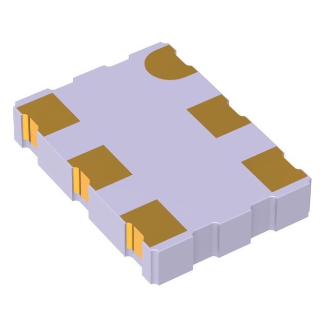
IDT8N4S272
6-lead ceramic 5mm x 7mm x 1.55mm
package body
CD Package
Top View
Configuration Register (ROM)
nOE
Pulldown
IDT8N4S272CCD REVISION A OCTOBER 3, 2012
1
©2012 Integrated Device Technology, Inc.
�IDT8N4S272 Data Sheet
LVDS FREQUENCY-PROGRAMMABLE CRYSTAL OSCILLATOR
Pin Description and Characteristic Tables
Table 1. Pin Descriptions
Number
Name
Type
Description
1
DNU
2
nOE
Input
3
GND
Power
Power supply ground.
4, 5
Q, nQ
Output
Differential clock output pair. LVDS interface levels.
6
VDD
Power
Power supply pin.
Do not use (factory use only).
Pulldown
Output enable pin. See Table 3A for function. LVCMOS/LVTTL interface levels.
NOTE: Pulldown refers to internal input resistors. See Table 2, Pin Characteristics, for typical values.
Table 2. Pin Characteristics
Symbol
Parameter
Test Conditions
Minimum
Typical
Maximum
Units
CIN
Input Capacitance
5.5
pF
RPULLDOWN
Input Pulldown Resistor
50
kΩ
Function Tables
Table 3A. nOE Configuration
Input
nOE
Output Enable
0 (default)
Outputs are enabled
1
Outputs Q, nQ are in high-impedance state
NOTE: nOE is an asynchronous control.
IDT8N4S272CCD REVISION A OCTOBER 3, 2012
2
©2012 Integrated Device Technology, Inc.
�IDT8N4S272 Data Sheet
LVDS FREQUENCY-PROGRAMMABLE CRYSTAL OSCILLATOR
Principles of Operation
Frequency Configuration
The block diagram consists of the internal 3rd overtone crystal and
oscillator which provide the reference clock fXTAL of either
An order code is assigned to each frequency configuration
programmed by the factory (default frequencies). For more
information on the available default frequencies and order codes,
please see the Ordering Information section in this document. For
available order codes, see the FemtoClock NG Ceramic-Package
XO and VCXO Ordering Product Information document.
114.285MHz or 100MHz. The PLL includes the FemtoClock NG
VCO along with the Pre-divider (P), the feedback divider (M) and the
post divider (N). The P, M, and N dividers determine the output frequency based on the fXTAL reference. The feedback divider is frac-
For more information on programming capabilities of the device for
custom frequency and pull-range configurations, see the FemtoClock
NG Ceramic 5x7 Module Programming Guide.
tional supporting a huge number of output frequencies. The
configuration of the feedback divider to integer-only values results in
an improved output phase noise characteristics at the expense of
the range of output frequencies. Internal registers are used to hold
one factory pre-set P, M, and N configuration setting. The P, M, and
N frequency configuration supports an output frequency range from
15.476MHz to 866.67MHz and from 975MHz to 1,300MHz.
Table 3B. Output Frequency Range1
15.476MHz to 866.67MHz
The devices use the fractional feedback divider with a delta-sigma
modulator for noise shaping and robust frequency synthesis
capability. The relatively high reference frequency minimizes phase
noise generated by frequency multiplication and allows more efficient
shaping of noise by the delta-sigma modulator.
975MHz to 1,300MHz
1. Supported output frequency range. The output frequency can
be programmed to any frequency in this range and to a precision of
218Hz or better.
The output frequency is determined by the 2-bit pre-divider (P), the
feedback divider (M) and the 7-bit post divider (N). The feedback
divider (M) consists of both a 7-bit integer portion (MINT) and an
18-bit fractional portion (MFRAC) and provides the means for
high-resolution frequency generation. The output frequency fOUT is
calculated by:
f
OUT
= f
1
MFRAC
+ 0.5-----------------------------------⋅ ----------- ⋅
XTAL P ⋅ N-- MINT +
18
2
IDT8N4S272CCD REVISION A OCTOBER 3, 2012
3
©2012 Integrated Device Technology, Inc.
�IDT8N4S272 Data Sheet
LVDS FREQUENCY-PROGRAMMABLE CRYSTAL OSCILLATOR
Absolute Maximum Ratings
NOTE: Stresses beyond those listed under Absolute Maximum
Ratings may cause permanent damage to the device. These ratings
are stress specifications only. Functional operation of product at
these conditions or any conditions beyond those listed in the DC
Characteristics or AC Characteristics is not implied. Exposure to
absolute maximum rating conditions for extended periods may affect
product reliability.
Item
Rating
Supply Voltage, VDD
3.63V
Inputs, VI
-0.5V to VDD + 0.5V
Outputs, IO (LVDS)
Continuous Current
Surge Current
10mA
15mA
Package Thermal Impedance, θJA
49.4°C/W (0 mps)
Storage Temperature, TSTG
-65°C to 150°C
DC Electrical Characteristics
Table 4A. Power Supply DC Characteristics, VDD = 3.3V ± 5%, TA = -40°C to 85°C
Symbol
Parameter
VDD
Power Supply Voltage
IDD
Power Supply Current
Test Conditions
Minimum
Typical
Maximum
Units
3.135
3.3
3.465
V
134
160
mA
Minimum
Typical
Maximum
Units
2.375
2.5
2.625
V
129
155
mA
Maximum
Units
Table 4B. Power Supply DC Characteristics, VDD = 2.5V ± 5%, TA = -40°C to 85°C
Symbol
Parameter
VDD
Power Supply Voltage
IDD
Power Supply Current
Test Conditions
Table 4C. LVCMOS/LVTTL DC Characteristic, VDD = 3.3V ± 5% or 2.5V ± 5%, TA = -40°C to 85°C
Symbol
Parameter
VIH
Input High Voltage
nOE
VIL
Input Low Voltage
nOE
IIH
Input High Current
nOE
VDD = VIN = 3.465V or 2.625V
IIL
Input Low Current
nOE
VDD = 3.465V or 2.625V, VIN = 0V
IDT8N4S272CCD REVISION A OCTOBER 3, 2012
Test Conditions
Minimum
VDD = 3.3V
2
VDD + 0.3
V
VDD = 2.5V
1.7
VDD + 0.3
V
VDD = 3.3V
-0.3
0.8
V
VDD = 2.5V
-0.3
0.7
V
150
µA
4
-10
Typical
µA
©2012 Integrated Device Technology, Inc.
�IDT8N4S272 Data Sheet
LVDS FREQUENCY-PROGRAMMABLE CRYSTAL OSCILLATOR
Table 4D. LVDS DC Characteristics, VDD = 3.3V ± 5%, TA = -40°C to 85°C
Symbol
Parameter
VOD
Differential Output Voltage
∆VOD
VOD Magnitude Change
VOS
Offset Voltage
∆VOS
VOS Magnitude Change
Test Conditions
Minimum
Typical
Maximum
Units
247
370
454
mV
50
mV
1.375
V
50
mV
1.125
1.22
Table 4E. LVDS DC Characteristics, VDD = 2.5V ± 5%, TA = -40°C to 85°C
Symbol
Parameter
VOD
Differential Output Voltage
∆VOD
VOD Magnitude Change
VOS
Offset Voltage
∆VOS
VOS Magnitude Change
IDT8N4S272CCD REVISION A OCTOBER 3, 2012
Test Conditions
Minimum
Typical
Maximum
Units
247
360
454
mV
50
mV
1.375
V
50
mV
1.125
5
1.21
©2012 Integrated Device Technology, Inc.
�IDT8N4S272 Data Sheet
LVDS FREQUENCY-PROGRAMMABLE CRYSTAL OSCILLATOR
AC Electrical Characteristics
Table 5. AC Characteristics, VDD = 3.3V ± 5% or 2.5V ± 5%, TA = -40°C to 85°C
Symbol
Parameter
fOUT
Output Frequency
fI
Initial Accuracy
Maximum
Units
15.476
866.67
MHz
975
1,300
MHz
Measured @ 25°C
±10
ppm
Option code = A or B
±100
ppm
Option code = E or F
±50
ppm
Option code = K or L
±20
ppm
Frequency drift over 10 year life
±3
ppm
Frequency drift over 15 year life
±5
ppm
Option code A, B (10 year life)
±113
ppm
Option code E, F (10 year life)
±63
ppm
Option code K, L (10 year life)
±33
ppm
20
ps
3
5
ps
17MHz ≤ fOUT ≤ 1300MHz,
Integration Range: 12kHz-20MHz
0.497
0.882
ps
500MHz ≤ fOUT ≤ 1300MHz,
Integration Range: 12kHz-20MHz
0.232
0.322
ps
125MHz ≤ fOUT < 500MHz,
Integration Range: 12kHz-20MHz
0.250
0.450
ps
17MHz ≤ fOUT < 125MHz,
Integration Range: 12kHz-20MHz
0.275
0.405
ps
fOUT = 156.25MHz,
Integration Range: 12kHz-20MHz
0.242
0.311
ps
fOUT = 231.25MHz,
Integration Range: 12kHz-20MHz
0.476
0.680
ps
fOUT = 156.25MHz,
Integration Range: 1kHz-40MHz
0.275
0.359
ps
fOUT = 231.25MHz,
Integration Range: 1kHz-40MHz
0.504
0.700
ps
RMS Phase Jitter (Random)
Fractional PLL feedback and
fXTAL=114.285MHz (0xxx order
codes), NOTE 2, 3
17MHz ≤ fOUT ≤ 1300MHz,
Integration Range: 12kHz-20MHz
0.474
0.986
ps
ΦN(100)
Single-side Band Phase Noise,
100Hz from Carrier
231.25MHz
-88
dBc/Hz
ΦN(1k)
Single-side Band Phase Noise,
1kHz from Carrier
231.25MHz
-110
dBc/Hz
ΦN(10k)
Single-side Band Phase Noise,
10kHz from Carrier
231.25MHz
-123
dBc/Hz
ΦN(100k)
Single-side Band Phase Noise,
100kHz from Carrier
231.25MHz
-125
dBc/Hz
ΦN(1M)
Single-side Band Phase Noise,
1MHz from Carrier
231.25MHz
-137
dBc/Hz
fS
Temperature Stability
fA
Aging
fT
Total Stability
tjit(cc)
Cycle-to-Cycle Jitter; NOTE 1
tjit(per)
RMS Period Jitter; NOTE 1
RMS Phase Jitter (Random);
Fractional PLL feedback and
fXTAL=100.000MHz (2xxx order
codes), NOTE 2, 3
tjit(Ø)
RMS Phase Jitter (Random);
Integer PLL feedback and
fXTAL=100.00MHz (1xxx order
codes), NOTE 2, 3
IDT8N4S272CCD REVISION A OCTOBER 3, 2012
Test Conditions
6
Minimum
Typical
©2012 Integrated Device Technology, Inc.
�IDT8N4S272 Data Sheet
LVDS FREQUENCY-PROGRAMMABLE CRYSTAL OSCILLATOR
Table 5. AC Characteristics, VDD = 3.3V ± 5% or 2.5V ± 5%, TA = -40°C to 85°C
Symbol
Parameter
Test Conditions
ΦN(10M)
Single-side band phase noise,
10MHz from Carrier
231.25MHz
tR / tF
Output Rise/Fall Time
20% to 80%
odc
Output Duty Cycle
tSTARTUP
Device Startup Time After
Power Up
Minimum
Typical
Maximum
-141
Units
dBc/Hz
50
450
ps
47
53
%
20
ms
NOTE: Electrical parameters are guaranteed over the specified ambient operating temperature range, which is established when the device is
mounted in a test socket with maintained transverse airflow greater than 500lfpm. The device will meet specifications after thermal equilibrium
has been reached under these conditions.
NOTE: XTAL parameters (initial accuracy, temperature stability, aging and total stability) are guaranteed by manufacturing.
NOTE 1: This parameter is defined in accordance with JEDEC standard 65.
NOTE 2: Please refer to the phase noise plot.
NOTE 3: Please see the FemtoClock NG Ceramic 5x7 Modules Programming guide for more information on PLL feedback modes and the
optimum configuration for phase noise. Integer PLL feedback is the default operation for the dddd = 1xxx order codes.
IDT8N4S272CCD REVISION A OCTOBER 3, 2012
7
©2012 Integrated Device Technology, Inc.
�IDT8N4S272 Data Sheet
LVDS FREQUENCY-PROGRAMMABLE CRYSTAL OSCILLATOR
Noise Power
dBc
Hz
Typical Phase Noise at 231.25MHz (12kHz - 20MHz)
Offset Frequency (Hz)
IDT8N4S272CCD REVISION A OCTOBER 3, 2012
8
©2012 Integrated Device Technology, Inc.
�IDT8N4S272 Data Sheet
LVDS FREQUENCY-PROGRAMMABLE CRYSTAL OSCILLATOR
Parameter Measurement Information
SCOPE
VDD
2.5V±5% POWER
SUPPLY
+ Float GND –
SCOPE
Q
3.3V±5% POWER
SUPPLY
+ Float GND –
Q
VDD
nQ
nQ
2.5V LVDS Output Load AC Test Circuit
3.3V LVDS Output Load AC Test Circuit
Phase Noise Plot
Noise Power
VOH
VREF
VOL
1σ contains 68.26% of all measurements
2σ contains 95.4% of all measurements
3σ contains 99.73% of all measurements
4σ contains 99.99366% of all measurements
6σ contains (100-1.973x10⁻⁷)% of all measurements
Offset Frequency
f1
f2
RMS Phase Jitter =
1
* Area Under Curve Defined by the Offset Frequency Markers
2* *ƒ
Histogram
Reference Point
Mean Period
(Trigger Edge)
(First edge after trigger)
RMS Phase Jitter
RMS Period Jitter
nQ
nQ
Q
Q
t PW
tcycle n
➤
tcycle n+1
t
➤
tjit(cc) = |tcycle n – tcycle n+1|
1000 Cycles
PERIOD
t
odc =
t
Cycle-to-Cycle Jitter
IDT8N4S272CCD REVISION A OCTOBER 3, 2012
PW
x 100%
PERIOD
Output Duty Cycle/Pulse Width/Period
9
©2012 Integrated Device Technology, Inc.
�IDT8N4S272 Data Sheet
LVDS FREQUENCY-PROGRAMMABLE CRYSTAL OSCILLATOR
Parameter Measurement Information, continued
VDD
nQ
80%
out
80%
VOD
Q
DC Input
LVDS
20%
20%
tR
tF
out
Output Rise/Fall Time
V OS/Δ V OS
Offset Voltage Setup
VDD
out
DC Input
LVDS
100
out
Differential Output Voltage Setup
IDT8N4S272CCD REVISION A OCTOBER 3, 2012
10
©2012 Integrated Device Technology, Inc.
�IDT8N4S272 Data Sheet
LVDS FREQUENCY-PROGRAMMABLE CRYSTAL OSCILLATOR
Applications Information
LVDS Driver Termination
For a general LVDS interface, the recommended value for the
termination impedance (ZT) is between 90Ω and 132Ω. The actual
value should be selected to match the differential impedance (Z0) of
your transmission line. A typical point-to-point LVDS design uses a
100Ω parallel resistor at the receiver and a 100Ω differential
transmission-line environment. In order to avoid any
transmission-line reflection issues, the components should be
surface mounted and must be placed as close to the receiver as
possible. IDT offers a full line of LVDS compliant devices with two
types of output structures: current source and voltage source. The
LVDS
Driver
standard termination schematic as shown in Figure 1A can be used
with either type of output structure. Figure 1B, which can also be
used with both output types, is an optional termination with center tap
capacitance to help filter common mode noise. The capacitor value
should be approximately 50pF. If using a non-standard termination, it
is recommended to contact IDT and confirm if the output structure is
current source or voltage source type. In addition, since these
outputs are LVDS compatible, the input receiver’s amplitude and
common-mode input range should be verified for compatibility with
the output.
ZO ≈ ZT
ZT
LVDS
Receiver
Figure 1A. Standard Termination
LVDS
Driver
ZO ≈ ZT
C
ZT
2 LVDS
ZT Receiver
2
Figure 1B. Optional Termination
IDT8N4S272CCD REVISION A OCTOBER 3, 2012
11
©2012 Integrated Device Technology, Inc.
�IDT8N4S272 Data Sheet
LVDS FREQUENCY-PROGRAMMABLE CRYSTAL OSCILLATOR
Schematic Layout
Figure 2 shows an example IDT8N4S272 application schematic. The
schematic example focuses on functional connections and is
intended as an example only and may not represent the exact user
configuration. Refer to the pin description and functional tables in the
datasheet to ensure the logic control inputs are properly set. For
example nOE can be configured from an FPGA instead of set with
pull up and pull down resistors as shown.
capacitor on the VDD pin must be placed on the device side with
direct return to the ground plane though vias. The remaining filter
components can be on the opposite side of the PCB.
Power supply filter component recommendations are a general
guideline to be used for reducing external noise from coupling into
the devices. The filter performance is designed for a wide range of
noise frequencies. This low-pass filter starts to attenuate noise at
approximately 10kHz. If a specific frequency noise component is
known, such as switching power supplies frequencies, it is
recommended that component values be adjusted and if required,
additional filtering be added. Additionally, good general design
practices for power plane voltage stability suggests adding bulk
capacitance in the local area of all devices.
As with any high speed analog circuitry, the power supply pins are
vulnerable to random noise, so to achieve optimum jitter performance
isolation of the VDD pin from power supply is required. In order to
achieve the best possible filtering, it is recommended that the
placement of the filter components be on the device side of the PCB
as close to the power pins as possible. If space is limited, the 0.1µF
Logic Control Input Examples
VDD
Set Logic
Input to '1'
VDD
RU1
1K
Set Logic
Input to '0'
RU2
Not Install
To Logic
Input
pins
To Logic
Input
pins
RD2
1K
RD1
Not Install
3.3V
C4
10uF
U1
1
nOE
2
3
DNU
nOE
GND
VDD
Q
nQ
6
FB1
2
VDD
C3
0.1uF
4
1
BLM18BB221SN1
C5
0.1uF
Place 0.1uF bypass cap
directly adjacent to
the VDD pin.
Zo = 50 Ohm
R1
100
5
+
Zo = 50 Ohm
LVDS Receiv er
Figure 2. IDT8N4S272 Schematic Example
IDT8N4S272CCD REVISION A OCTOBER 3, 2012
12
©2012 Integrated Device Technology, Inc.
�IDT8N4S272 Data Sheet
LVDS FREQUENCY-PROGRAMMABLE CRYSTAL OSCILLATOR
Power Considerations
This section provides information on power dissipation and junction temperature for the IDT8N4S272.
Equations and example calculations are also provided.
1.
Power Dissipation.
The total power dissipation for the IDT8N4S272 is the sum of the core power plus the power dissipated due to loading. The following is the
power dissipation for VDD = 3.3V + 5% = 3.465V, which gives worst case results.
•
Power (core)MAX = VDD_MAX * IDD_MAX = 3.465V * 160mA = 554.4mW
2. Junction Temperature.
Junction temperature, Tj, is the temperature at the junction of the bond wire and bond pad directly affects the reliability of the device. The
maximum recommended junction temperature is 125°C. Limiting the internal transistor junction temperature, Tj, to 125°C ensures that the bond
wire and bond pad temperature remains below 125°C.
The equation for Tj is as follows: Tj = θJA * Pd_total + TA
Tj = Junction Temperature
θJA = Junction-to-Ambient Thermal Resistance
Pd_total = Total Device Power Dissipation (example calculation is in section 1 above)
TA = Ambient Temperature
In order to calculate junction temperature, the appropriate junction-to-ambient thermal resistance θJA must be used. Assuming no air flow and
a multi-layer board, the appropriate value is 49.4°C/W per Table 6 below.
Therefore, Tj for an ambient temperature of 85°C with all outputs switching is:
85°C + 0.554W * 49.4°C/W = 112.4°C. This is below the limit of 125°C.
This calculation is only an example. Tj will obviously vary depending on the number of loaded outputs, supply voltage, air flow and the type of
board (multi-layer).
Table 6. Thermal Resistance θJA for 6 Lead Ceramic 5mm x 7mm Package, Forced Convection
θJA by Velocity
Meters per Second
Multi-Layer PCB, JEDEC Standard Test Boards
IDT8N4S272CCD REVISION A OCTOBER 3, 2012
0
1
2
49.4°C/W
44.2°C/W
42.1°C/W
13
©2012 Integrated Device Technology, Inc.
�IDT8N4S272 Data Sheet
LVDS FREQUENCY-PROGRAMMABLE CRYSTAL OSCILLATOR
Reliability Information
Table 7. θJA vs. Air Flow Table for a 6-lead Ceramic 5mm x 7mm Package
θJA vs. Air Flow
Meters per Second
Multi-Layer PCB, JEDEC Standard Test Boards
0
1
2
49.4°C/W
44.2°C/W
42.1°C/W
Transistor Count
The transistor count for IDT8N4S272 is: 47,511
IDT8N4S272CCD REVISION A OCTOBER 3, 2012
14
©2012 Integrated Device Technology, Inc.
�cr:
u
.!:
,.:;
:5
Cl
0
:!
0
u
u
z
w
::::l
a
1.400 T YP.
w
cr:
LL.
7. 0 0±0.15
C
Ul
Cl
>
--'
trl±O?
2
) OOT IO
C/)
1::
0
C/)
1::
Q)
·cE-
I
4
5
1- -1
TYP.
0. 20 R REF.
0. 70 R
I JDEX
5.00 ±0.15
j
6
0.13 R
0...
i'=
REF.
Q)
tJ)
N
(.)
ctS
a..
DTE S:
Al l diMen sio ns 1 n M M
1'l
c0
0::
w
ClJ
""C
0
ctS
0
0
Q)
1::
0
1::
1-
"'
Ul
-