FemtoClock® NG Ultra-Performance
Jitter Attenuator
8T49N240
Datasheet
Description
Features
The 8T49N240 is a fractional-feedback single channel jitter
attenuator with frequency translation. It is equipped with three
integer and one fractional output dividers, allowing the generation
of up to four different output frequencies, ranging from 8kHz to
867MHz. These frequencies are completely independent of the
input reference frequencies and the crystal reference frequency.
The outputs may select among LVPECL, LVDS, HCSL, or
LVCMOS output levels.
▪ Four differential outputs
▪ Excellent jitter performance:
— < 200fs (typical) RMS (including spurs):
12kHz to 20MHz for integer-divider outputs in jitter
attenuator mode or in fractional-feedback synthesizer mode
▪ Operating Modes: Synthesizer, Jitter Attenuator
▪ Operates from a 10MHz to 54MHz fundamental-mode crystal
▪ Initial holdover accuracy of +50ppb
▪ Accepts up to two LVPECL, LVDS, LVHSTL, or LVCMOS input
clocks
— Accepts frequencies ranging from 8kHz to 875MHz
— Auto and manual clock selection with hitless switching
— Clock input monitoring including support for gapped clocks
▪ Phase-slope limiting and fully hitless switching options to
control output clock phase transients
▪ Three outputs generate LVPECL / LVDS / HCSL clocks, one
output generates LVPECL / LVDS / HCSL / LVCMOS clocks
— Output frequencies ranging from 8kHz up to 867MHz
(differential)
— Output frequencies ranging from 8kHz to 250MHz
(LVCMOS)
— Three integer dividers with fixed divider ratios (see Table 3)
— One fractional output divider
▪ Programmable loop bandwidth settings from 0.2Hz to 6.4kHz
— Optional fast-lock function
▪ Four General Purpose I/O pins with optional support for status
and control:
— Two Output Enable control inputs provide control over the
four clocks
— Manual clock selection control input
— Lock, Holdover, and Loss-of-Signal alarm outputs
▪ Open-drain Interrupt pin
▪ Register programmable through I2C or via external I2C
EEPROM
▪ Full 2.5V or 3.3V supply modes, with some support for 1.8V
▪ -40°C to 85°C ambient operating temperature
▪ Package: 6 x 6 x 0.9 mm 40-VFQFN, lead-free (RoHS 6)
The 8T49N240 accepts up to two differential or single-ended input
clocks and a fundamental-mode crystal input. The internal PLL
can lock to either of the input reference clocks or just to the crystal
to behave as a frequency synthesizer. The PLL can use the
second input for redundant backup of the primary input reference,
but in this case, both input clock references must be integer
related in frequency.
The device supports hitless reference switching between input
clocks. The device monitors both input clocks for Loss of Signal
(LOS), and generates an alarm when an input clock failure is
detected. Automatic and manual hitless reference switching
options are supported. LOS behavior can be set to support
gapped or un-gapped clocks.
The 8T49N240 supports holdover. The holdover has an initial
accuracy of ±50ppB from the point where the loss of all applicable
input reference(s) has been detected. It maintains a historical
average operating point for the PLL that may be returned to in
holdover at a limited phase slope.
The PLL has a register-selectable loop bandwidth from 0.2Hz to
6.4kHz.
The device supports Output Enable and Clock Select inputs and
Lock, Holdover, and LOS status outputs.
The device is programmable through an I2C interface. It also
supports I2C master capability to allow the register configuration
to be read from an external EEPROM.
Factory pre-programmed devices are also available using the
on-chip One Time Programmable (OTP) memory.
Typical Applications
▪
▪
▪
▪
▪
OTN, including ITU-T G.709 (2009) FEC
CPRI interfaces
Fiber optics
40G/100G Ethernet
Gb Ethernet, Terabit IP switches / routers
©2019 Integrated Device Technology, Inc.
1
January 15, 2019
�8T49N240 Datasheet
Contents
Description . . . . . . . . . . . . . . . . . . . . . . . . . . . . . . . . . . . . . . . . . . . . . . . . . . . . . . . . . . . . . . . . . . . . . . . . . . . . . . . . . . . . . . . . . . . . . . . . . . . . . . 1
Typical Applications . . . . . . . . . . . . . . . . . . . . . . . . . . . . . . . . . . . . . . . . . . . . . . . . . . . . . . . . . . . . . . . . . . . . . . . . . . . . . . . . . . . . . . . . . . . . . . . 1
Features . . . . . . . . . . . . . . . . . . . . . . . . . . . . . . . . . . . . . . . . . . . . . . . . . . . . . . . . . . . . . . . . . . . . . . . . . . . . . . . . . . . . . . . . . . . . . . . . . . . . . . . . 1
Block Diagram . . . . . . . . . . . . . . . . . . . . . . . . . . . . . . . . . . . . . . . . . . . . . . . . . . . . . . . . . . . . . . . . . . . . . . . . . . . . . . . . . . . . . . . . . . . . . . . . . . . 4
Pin Assignments. . . . . . . . . . . . . . . . . . . . . . . . . . . . . . . . . . . . . . . . . . . . . . . . . . . . . . . . . . . . . . . . . . . . . . . . . . . . . . . . . . . . . . . . . . . . . . . . . . 5
Pin Descriptions . . . . . . . . . . . . . . . . . . . . . . . . . . . . . . . . . . . . . . . . . . . . . . . . . . . . . . . . . . . . . . . . . . . . . . . . . . . . . . . . . . . . . . . . . . . . . . . . . . 5
Principles of Operation . . . . . . . . . . . . . . . . . . . . . . . . . . . . . . . . . . . . . . . . . . . . . . . . . . . . . . . . . . . . . . . . . . . . . . . . . . . . . . . . . . . . . . . . . . . . . 8
Crystal Input . . . . . . . . . . . . . . . . . . . . . . . . . . . . . . . . . . . . . . . . . . . . . . . . . . . . . . . . . . . . . . . . . . . . . . . . . . . . . . . . . . . . . . . . . . . . . . . . 8
Bypass Path . . . . . . . . . . . . . . . . . . . . . . . . . . . . . . . . . . . . . . . . . . . . . . . . . . . . . . . . . . . . . . . . . . . . . . . . . . . . . . . . . . . . . . . . . . . . . . . . 8
Input Clock Selection . . . . . . . . . . . . . . . . . . . . . . . . . . . . . . . . . . . . . . . . . . . . . . . . . . . . . . . . . . . . . . . . . . . . . . . . . . . . . . . . . . . . . . . . . 9
Input Clock Monitor . . . . . . . . . . . . . . . . . . . . . . . . . . . . . . . . . . . . . . . . . . . . . . . . . . . . . . . . . . . . . . . . . . . . . . . . . . . . . . . . . . . . . . . . . . . 9
Holdover . . . . . . . . . . . . . . . . . . . . . . . . . . . . . . . . . . . . . . . . . . . . . . . . . . . . . . . . . . . . . . . . . . . . . . . . . . . . . . . . . . . . . . . . . . . . . . . . . . 10
Input to Output Clock Frequency . . . . . . . . . . . . . . . . . . . . . . . . . . . . . . . . . . . . . . . . . . . . . . . . . . . . . . . . . . . . . . . . . . . . . . . . . . . . . . . 10
Synthesizer Mode Operation . . . . . . . . . . . . . . . . . . . . . . . . . . . . . . . . . . . . . . . . . . . . . . . . . . . . . . . . . . . . . . . . . . . . . . . . . . . . . . . . . . . 10
Loop Filter and Bandwidth . . . . . . . . . . . . . . . . . . . . . . . . . . . . . . . . . . . . . . . . . . . . . . . . . . . . . . . . . . . . . . . . . . . . . . . . . . . . . . . . . . . . 11
Integer Output Dividers (Q0, Q1 or Q2) . . . . . . . . . . . . . . . . . . . . . . . . . . . . . . . . . . . . . . . . . . . . . . . . . . . . . . . . . . . . . . . . . . . . . . . . . . 11
Fractional Output Divider Programming (Q3 Only) . . . . . . . . . . . . . . . . . . . . . . . . . . . . . . . . . . . . . . . . . . . . . . . . . . . . . . . . . . . . . . . . . . 11
Output Divider Frequency Sources . . . . . . . . . . . . . . . . . . . . . . . . . . . . . . . . . . . . . . . . . . . . . . . . . . . . . . . . . . . . . . . . . . . . . . . . . . . . . . 11
Output Phase Control on Switchover . . . . . . . . . . . . . . . . . . . . . . . . . . . . . . . . . . . . . . . . . . . . . . . . . . . . . . . . . . . . . . . . . . . . . . . . . . . . 12
Output Drivers . . . . . . . . . . . . . . . . . . . . . . . . . . . . . . . . . . . . . . . . . . . . . . . . . . . . . . . . . . . . . . . . . . . . . . . . . . . . . . . . . . . . . . . . . . . . . . 12
LVCMOS Operation (Q3 Only) . . . . . . . . . . . . . . . . . . . . . . . . . . . . . . . . . . . . . . . . . . . . . . . . . . . . . . . . . . . . . . . . . . . . . . . . . . . . . 12
Power-Saving Modes . . . . . . . . . . . . . . . . . . . . . . . . . . . . . . . . . . . . . . . . . . . . . . . . . . . . . . . . . . . . . . . . . . . . . . . . . . . . . . . . . . . . . . . . 12
Status / Control Signals and Interrupts . . . . . . . . . . . . . . . . . . . . . . . . . . . . . . . . . . . . . . . . . . . . . . . . . . . . . . . . . . . . . . . . . . . . . . . . . . . 12
General-Purpose I/Os and Interrupts . . . . . . . . . . . . . . . . . . . . . . . . . . . . . . . . . . . . . . . . . . . . . . . . . . . . . . . . . . . . . . . . . . . . . . . . 13
Interrupt Functionality . . . . . . . . . . . . . . . . . . . . . . . . . . . . . . . . . . . . . . . . . . . . . . . . . . . . . . . . . . . . . . . . . . . . . . . . . . . . . . . . . . . . 13
Output Enable Operation . . . . . . . . . . . . . . . . . . . . . . . . . . . . . . . . . . . . . . . . . . . . . . . . . . . . . . . . . . . . . . . . . . . . . . . . . . . . . . . . . 13
Device Hardware Configuration . . . . . . . . . . . . . . . . . . . . . . . . . . . . . . . . . . . . . . . . . . . . . . . . . . . . . . . . . . . . . . . . . . . . . . . . . . . . . . . . 14
Device Start-up and Reset Behavior . . . . . . . . . . . . . . . . . . . . . . . . . . . . . . . . . . . . . . . . . . . . . . . . . . . . . . . . . . . . . . . . . . . . . . . . . . . . . 14
Serial Control Port Description . . . . . . . . . . . . . . . . . . . . . . . . . . . . . . . . . . . . . . . . . . . . . . . . . . . . . . . . . . . . . . . . . . . . . . . . . . . . . . . . . 15
Serial Control Port Configuration Description . . . . . . . . . . . . . . . . . . . . . . . . . . . . . . . . . . . . . . . . . . . . . . . . . . . . . . . . . . . . . . . . . . 15
I2C Mode Operation . . . . . . . . . . . . . . . . . . . . . . . . . . . . . . . . . . . . . . . . . . . . . . . . . . . . . . . . . . . . . . . . . . . . . . . . . . . . . . . . . . . . . 15
I2C Master Mode . . . . . . . . . . . . . . . . . . . . . . . . . . . . . . . . . . . . . . . . . . . . . . . . . . . . . . . . . . . . . . . . . . . . . . . . . . . . . . . . . . . . . . . 16
I2C Boot-up Initialization Mode . . . . . . . . . . . . . . . . . . . . . . . . . . . . . . . . . . . . . . . . . . . . . . . . . . . . . . . . . . . . . . . . . . . . . . . . . . . . . 17
Absolute Maximum Ratings . . . . . . . . . . . . . . . . . . . . . . . . . . . . . . . . . . . . . . . . . . . . . . . . . . . . . . . . . . . . . . . . . . . . . . . . . . . . . . . . . . . . . . . . 40
Supply Voltage Characteristics . . . . . . . . . . . . . . . . . . . . . . . . . . . . . . . . . . . . . . . . . . . . . . . . . . . . . . . . . . . . . . . . . . . . . . . . . . . . . . . . . . . . . 40
DC Electrical Characteristics . . . . . . . . . . . . . . . . . . . . . . . . . . . . . . . . . . . . . . . . . . . . . . . . . . . . . . . . . . . . . . . . . . . . . . . . . . . . . . . . . . . . . . . 42
AC Electrical Characteristics . . . . . . . . . . . . . . . . . . . . . . . . . . . . . . . . . . . . . . . . . . . . . . . . . . . . . . . . . . . . . . . . . . . . . . . . . . . . . . . . . . . . . . . 45
Typical Phase Noise at 156.25MHz . . . . . . . . . . . . . . . . . . . . . . . . . . . . . . . . . . . . . . . . . . . . . . . . . . . . . . . . . . . . . . . . . . . . . . . . . . . . . 52
Applications Information . . . . . . . . . . . . . . . . . . . . . . . . . . . . . . . . . . . . . . . . . . . . . . . . . . . . . . . . . . . . . . . . . . . . . . . . . . . . . . . . . . . . . . . . . . . 53
Recommendations for Unused Input and Output Pins . . . . . . . . . . . . . . . . . . . . . . . . . . . . . . . . . . . . . . . . . . . . . . . . . . . . . . . . . . . . . . . 53
Inputs . . . . . . . . . . . . . . . . . . . . . . . . . . . . . . . . . . . . . . . . . . . . . . . . . . . . . . . . . . . . . . . . . . . . . . . . . . . . . . . . . . . . . . . . . . . . . . . . 53
Outputs . . . . . . . . . . . . . . . . . . . . . . . . . . . . . . . . . . . . . . . . . . . . . . . . . . . . . . . . . . . . . . . . . . . . . . . . . . . . . . . . . . . . . . . . . . . . . . . 53
Overdriving the XTAL Interface . . . . . . . . . . . . . . . . . . . . . . . . . . . . . . . . . . . . . . . . . . . . . . . . . . . . . . . . . . . . . . . . . . . . . . . . . . . . . . . . . 54
Wiring the Differential Input to Accept Single-Ended Levels . . . . . . . . . . . . . . . . . . . . . . . . . . . . . . . . . . . . . . . . . . . . . . . . . . . . . . . . . . . 55
3.3V Differential Clock Input Interface . . . . . . . . . . . . . . . . . . . . . . . . . . . . . . . . . . . . . . . . . . . . . . . . . . . . . . . . . . . . . . . . . . . . . . . . . . . . 56
2.5V Differential Clock Input Interface . . . . . . . . . . . . . . . . . . . . . . . . . . . . . . . . . . . . . . . . . . . . . . . . . . . . . . . . . . . . . . . . . . . . . . . . . . . . 57
LVDS Driver Termination . . . . . . . . . . . . . . . . . . . . . . . . . . . . . . . . . . . . . . . . . . . . . . . . . . . . . . . . . . . . . . . . . . . . . . . . . . . . . . . . . . . . . 58
Termination for 3.3V LVPECL Outputs . . . . . . . . . . . . . . . . . . . . . . . . . . . . . . . . . . . . . . . . . . . . . . . . . . . . . . . . . . . . . . . . . . . . . . . . . . . 59
©2019 Integrated Device Technology, Inc.
2
January 15, 2019
�8T49N240 Datasheet
Termination for 2.5V LVPECL Outputs . . . . . . . . . . . . . . . . . . . . . . . . . . . . . . . . . . . . . . . . . . . . . . . . . . . . . . . . . . . . . . . . . . . . . . . . . . .
HCSL Recommended Termination . . . . . . . . . . . . . . . . . . . . . . . . . . . . . . . . . . . . . . . . . . . . . . . . . . . . . . . . . . . . . . . . . . . . . . . . . . . . . .
VFQFN EPAD Thermal Release Path . . . . . . . . . . . . . . . . . . . . . . . . . . . . . . . . . . . . . . . . . . . . . . . . . . . . . . . . . . . . . . . . . . . . . . . . . . .
Schematic and Layout Information . . . . . . . . . . . . . . . . . . . . . . . . . . . . . . . . . . . . . . . . . . . . . . . . . . . . . . . . . . . . . . . . . . . . . . . . . . . . . .
Crystal Recommendation . . . . . . . . . . . . . . . . . . . . . . . . . . . . . . . . . . . . . . . . . . . . . . . . . . . . . . . . . . . . . . . . . . . . . . . . . . . . . . . . . . . . .
PCI Express Application Note . . . . . . . . . . . . . . . . . . . . . . . . . . . . . . . . . . . . . . . . . . . . . . . . . . . . . . . . . . . . . . . . . . . . . . . . . . . . . . . . . .
Power Dissipation and Thermal Considerations. . . . . . . . . . . . . . . . . . . . . . . . . . . . . . . . . . . . . . . . . . . . . . . . . . . . . . . . . . . . . . . . . . . . . . . . .
Power Domains . . . . . . . . . . . . . . . . . . . . . . . . . . . . . . . . . . . . . . . . . . . . . . . . . . . . . . . . . . . . . . . . . . . . . . . . . . . . . . . . . . . . . . . . . . . . .
Power Consumption Calculation . . . . . . . . . . . . . . . . . . . . . . . . . . . . . . . . . . . . . . . . . . . . . . . . . . . . . . . . . . . . . . . . . . . . . . . . . . . . . . . .
Thermal Considerations . . . . . . . . . . . . . . . . . . . . . . . . . . . . . . . . . . . . . . . . . . . . . . . . . . . . . . . . . . . . . . . . . . . . . . . . . . . . . . . . . . . . . .
Current Consumption Data and Equations . . . . . . . . . . . . . . . . . . . . . . . . . . . . . . . . . . . . . . . . . . . . . . . . . . . . . . . . . . . . . . . . . . . . . . . .
Example Calculations . . . . . . . . . . . . . . . . . . . . . . . . . . . . . . . . . . . . . . . . . . . . . . . . . . . . . . . . . . . . . . . . . . . . . . . . . . . . . . . . . . . . . . . .
Reliability Information . . . . . . . . . . . . . . . . . . . . . . . . . . . . . . . . . . . . . . . . . . . . . . . . . . . . . . . . . . . . . . . . . . . . . . . . . . . . . . . . . . . . . . . . . . . . .
Transistor Count . . . . . . . . . . . . . . . . . . . . . . . . . . . . . . . . . . . . . . . . . . . . . . . . . . . . . . . . . . . . . . . . . . . . . . . . . . . . . . . . . . . . . . . . . . . .
Package Outlines Drawings . . . . . . . . . . . . . . . . . . . . . . . . . . . . . . . . . . . . . . . . . . . . . . . . . . . . . . . . . . . . . . . . . . . . . . . . . . . . . . . . . . . . . . . .
Marking Diagram . . . . . . . . . . . . . . . . . . . . . . . . . . . . . . . . . . . . . . . . . . . . . . . . . . . . . . . . . . . . . . . . . . . . . . . . . . . . . . . . . . . . . . . . . . . . . . . .
Ordering Information . . . . . . . . . . . . . . . . . . . . . . . . . . . . . . . . . . . . . . . . . . . . . . . . . . . . . . . . . . . . . . . . . . . . . . . . . . . . . . . . . . . . . . . . . . . . .
Revision History . . . . . . . . . . . . . . . . . . . . . . . . . . . . . . . . . . . . . . . . . . . . . . . . . . . . . . . . . . . . . . . . . . . . . . . . . . . . . . . . . . . . . . . . . . . . . . . . .
©2019 Integrated Device Technology, Inc.
3
60
61
62
62
62
63
64
64
64
65
65
68
71
71
71
71
71
73
January 15, 2019
�8T49N240 Datasheet
Block Diagram
S_A
©2019 Integrated Device Technology, Inc.
4
January 15, 2019
�8T49N240 Datasheet
Pin Assignments
VCCO2
Q2
nQ2
GPIO[2]
nQ3
Q3
VCCO3
GPIO[3]
nINT
VCCA
Figure 1. Pin Assignments for 6mm x 6mm 40-Lead VFQFN Package
30 29 28 27 26 25 24 23 22 21
nRST
31
20
S_A0
VCCA
32
19
nCLK1
OSCI
33
18
CLK1
OSCO
34
17
nCLK0
S_A1
35
16
CLK0
VCCCS
36
15
VCC
CAP1
37
14
VEE
CAP2
38
13
VCC
CAP_REF
39
12
SCLK
11
SDATA
1
2
3
4
5
6
7
8
9
10
VCCA
GPIO[0]
VCCO0
Q0
nQ0
GPIO[1]
nQ1
Q1
VCCO1
40
VCCA
VCCA
8T49N240
Pin Descriptions
Table 1. Pin Descriptions [a]
Number
Name
Type
1
VCCA
Power
Analog function supply for core analog functions. 2.5V or 3.3V supported.
2
VCCA
Power
Analog function supply for analog functions associated with PLL. 2.5V or 3.3V
supported.
3
GPIO[0]
I/O
4
VCCO0
Power
5
Q0
O
Universal
Output Clock 0. For more information, see Output Drivers.
6
nQ0
O
Universal
Output Clock 0. For more information, see Output Drivers.
7
GPIO[1]
I/O
Pullup
8
nQ1
O
Universal
Output Clock 1. For more information, see Output Drivers.
9
Q1
O
Universal
Output Clock 1. For more information, see Output Drivers.
10
VCCO1
Power
11
SDATA
I/O
Pullup
I2C interface bi-directional data.
12
SCLK
I/O
Pullup
I2C interface bi-directional clock.
©2019 Integrated Device Technology, Inc.
Description
Pullup
General-purpose input-output. LVTTL / LVCMOS Input levels.
High-speed output supply for output pair Q0, nQ0. 2.5V or 3.3V supported for
differential output types. LVCMOS outputs also support 1.8V.
General-purpose input-output. LVTTL / LVCMOS Input levels.
High-speed output supply for output pair Q1, nQ1. 2.5V or 3.3V supported for
differential output types. LVCMOS outputs also support 1.8V.
5
January 15, 2019
�8T49N240 Datasheet
Table 1. Pin Descriptions [a] (Cont.)
Number
Name
Type
Description
13
VCC
Power
Core digital function supply. 2.5V or 3.3V supported.
14
EPAD
VEE
Power
Negative supply voltage. All VEE pins and EPAD must be connected before any
positive supply voltage is applied.
15
VCC
Power
Core digital function supply. 2.5V or 3.3V supported.
16
CLK0
I
Pulldown
Non-inverting differential clock input 0.
17
nCLK0
I
Pullup /
Pulldown
Inverting differential clock input 0.
VCC / 2 when left floating (set by internal pullup / pulldown resistors)
18
CLK1
I
Pulldown
Non-inverting differential clock input 1.
19
nCLK1
I
Pullup /
Pulldown
Inverting differential clock input 1.
VCC / 2 when left floating (set by internal pullup / pulldown resistors)
20
S_A0
I
Pulldown
I2C Address Bit A0.
21
VCCO2
Power
22
Q2
O
Universal
Output Clock 2. For more information, see Output Drivers.
23
nQ2
O
Universal
Output Clock 2. For more information, see Output Drivers.
24
GPIO[2]
I/O
Pullup
25
nQ3
O
Universal
Output Clock 3. For more information, see Output Drivers.
26
Q3
O
Universal
Output Clock 3. For more information, see Output Drivers.
27
VCCO3
Power
28
GPIO[3]
I/O
Pullup
29
nINT
O
Open-drain
with pullup
30
VCCA
Power
31
nRST
I
32
VCCA
Power
33
OSCI
I
Crystal Input. Accepts a 10MHz - 54MHz reference from a clock oscillator or a
12pF fundamental mode, parallel-resonant crystal.
34
OSCO
O
Crystal Output. This pin should be connected to a crystal. If an oscillator is
connected to OSCI, then this pin must be left unconnected.
35
S_A1
I
High-speed output supply voltage for output pair Q2, nQ2. 2.5V or 3.3V
supported for differential output types. LVCMOS outputs also support 1.8V.
General-purpose input-output. LVTTL / LVCMOS Input levels.
High-speed output supply voltage for output pair Q3, nQ3. 2.5V or 3.3V
supported for differential output types. LVCMOS outputs also support 1.8V.
General-purpose input-output. LVTTL / LVCMOS Input levels.
Interrupt output.
Analog function supply for analog functions associated with PLL. 2.5V or 3.3V
supported.
Pullup
Master Reset input> LVTTL / LVCMOS interface levels:
0 = All registers and state machines are reset to their default values
1 = Device runs normally
Analog function supply for core analog functions. 2.5V or 3.3V supported.
Pulldown
I2C Address bit A1.
36
VCCCS
Power
Output supply for Control and Status pins:
GPIO[3:0], SDATA, SCLK, S_A0, nINT, nRST,S_A1
1.8V, 2.5V, or 3.3V supported.
37
CAP1
Analog
PLL External Capacitance.
©2019 Integrated Device Technology, Inc.
6
January 15, 2019
�8T49N240 Datasheet
Table 1. Pin Descriptions [a] (Cont.)
Number
Name
Type
Description
38
CAP2
Analog
PLL External Capacitance.
39
CAP_REF
Analog
External Capacitance for input reference clock circuitry.
40
VCCA
Power
Analog function supply for analog functions associated with PLL. 2.5V or 3.3V
supported.
[a] Pullup and Pulldown refer to internal input resistors. See Table 2, Pin Characteristics, for typical values.
Table 2. Pin Characteristics, VCC = VCCOX[a] = 3.3V±5% or 2.5V±5%
Symbol
Parameter
CIN
Input Capacitance[b]
CXTAL
Test Conditions
Minimum
Typical
Maximum
Units
3.5
pF
Crystal Pins (OSCI, OSCO) Internal
Capacitance
8
pF
RPULLUP
Input
Pullup Resistor
SDATA, SCLK,
nRST, GPIO[3:0]
51
k
RPULLDOWN
Input
Pulldown Resistor
S_A0, S_A1
51
k
VCCOX = 3.465V
13
pF
VCCOX = 2.625V
15
pF
VCCOX = 1.89V
15
pF
LVDS, HCSL or
LVPECL Q[0:2]
2.5
pF
Q3, LVDS, HCSL
or LVPECL
4.5
pF
VCCCS = 3.3V
26
VCCCS = 2.5V
32
VCCCS = 1.8V
39
VCCOX = 3.3V
18
VCCOX = 2.5V
18
VCCOX = 1.8V
24
Q3, LVCMOS
CPD
Power Dissipation
Capacitance
(per output pair)
GPIO[3:0]
ROUT
Output
Impedance
LVCMOS
Q3, nQ3
[a] VCCOX denotes: VCCO0, VCCO1, VCCO2 or VCCO3.
[b] This specification does not apply to the OSCI or OSCO pins.
©2019 Integrated Device Technology, Inc.
7
January 15, 2019
�8T49N240 Datasheet
Principles of Operation
The 8T49N240 can be locked to either of the input clocks and generate a wide range of synchronized output clocks. It could be used for
example in either the transmit or receive path of Synchronous Ethernet equipment.
The 8T49N240 accepts up to two differential or single-ended input clocks ranging from 8kHz up to 875MHz. It generates up to four output
clocks ranging from 8kHz up to 867MHz.
The PLL path within the 8T49N240 supports three states: Lock, Holdover and Free-run. Lock and holdover status may be monitored on
register bits and pins. The PLL also supports automatic and manual hitless reference switching. In the locked state, the PLL locks to a
valid clock input and its output clocks have a frequency accuracy equal to the frequency accuracy of the input clock. In the Holdover
state, the PLL will output a clock which is based on the selected holdover behavior. The PLL within the 8T49N240 has an initial holdover
frequency offset of ±50ppb. In the Free-run state, the PLL outputs a clock with the same frequency accuracy as the external crystal.
Upon power up, the PLL will enter Free-run state, in this state it generates output clocks with the same frequency accuracy as the
external crystal. The 8T49N240 continuously monitors each input for activity (signal transitions). If no input references are provided, the
device will remain locked to the crystal in Free-run state and will generate output frequencies as a synthesizer.
When an input clock has been validated the PLL will transition to the Lock state. In automatic reference switching, if the selected input
clock fails and there are no other valid input clocks, the PLL will quickly detect that and go into Holdover. In the Holdover state, the PLL
will output a clock which is based on the selected holdover behavior. If the selected input clock fails and another input clock is available
then the 8T49N240 will hitlessly switch to that input clock. The reference switch can be either revertive or non-revertive. Manual
switchover is also available with switchover only occurring on user command, either via register bit or via the Clock Select input function
of the GPIO[3:0] pins.
The device supports conversion of any input frequencies to four different output frequencies: one independent output frequency on Q3
and three more integer-related frequencies on Q[0:2].
The 8T49N240 has a programmable loop bandwidth from 0.2Hz to 6.4kHz.
The device monitors all input clocks and generates an alarm when an input clock failure is detected.
The device is programmable through an I2C and may also autonomously read its register settings from an internal One-Time
Programmable (OTP) memory or an external serial I2C EEPROM.
Crystal Input
The crystal input on the 8T49N240 is capable of being driven by a parallel-resonant, fundamental mode crystal with a frequency range of
10MHz - 54MHz
The oscillator input also supports being driven by a single-ended crystal oscillator or reference clock.
The initial holdover frequency offset is set by the device, but the long term drift depends on the quality of the crystal or oscillator attached
to this port.
Bypass Path
The crystal input, CLK0 or CLK1 may be used directly as a clock source for the Q[3] output divider. This may only be done for input
frequencies of 250MHz or less.
©2019 Integrated Device Technology, Inc.
8
January 15, 2019
�8T49N240 Datasheet
Input Clock Selection
The 8T49N240 accepts up to two input clocks with frequencies ranging from 8kHz up to 875MHz. Each input can accept LVPECL, LVDS,
LVHSTL, HCSL or LVCMOS inputs using 1.8V, 2.5V or 3.3V logic levels.
In Manual mode, only one of the inputs may be chosen and if that input fails that PLL will enter holdover.
Manual mode may be operated by directly selecting the desired input reference in the REFSEL register field. It may also operate via
pin-selection of the desired input clock by selecting that mode in the REFSEL register field. In that case, GPIO[2] must be used as a
Clock Select input (CSEL). CSEL = 0 will select the CLK0 input and CSEL = 1 will select the CLK1 input.
In addition, the crystal frequency may be passed directly to the output divider Q[3] for use as a reference.
Inputs do not support transmission of spread-spectrum clocking sources. Since this family is intended for high-performance applications,
it will assume input reference sources to have stabilities of +100ppm or better, except where gapped clock inputs are used.
If the PLL is working in automatic mode, then one of the input reference sources is assigned as the higher priority. At power-up or if the
currently selected input reference fails, the PLL will switch to the highest priority input reference that is valid at that time (see Input Clock
Monitor section for details).
Automatic mode has two sub-options: revertive or non-revertive. In revertive mode, the PLL will switch to a reference with a higher priority
setting whenever one becomes valid. In non-revertive mode the PLL remains with the currently selected source as long as it remains
valid.
The clock input selection is based on the input clock priority set by the Clock Input Priority control bit.
Input Clock Monitor
Each clock input is monitored for Loss of Signal (LOS). If no activity has been detected on the clock input within a user-selectable time
period then the clock input is considered to be failed and an internal Loss-of-Signal status flag is set, which may cause an input
switchover depending on other settings. The user-selectable time period has sufficient range to allow a gapped clock missing many
consecutive edges to be considered a valid input.
User-selection of the clock monitor time-period is based on a counter driven by a monitor clock. The monitor clock is fixed at the
frequency of the PLL’s VCO divided by 8. With a VCO range of 2.44GHz - 2.6GHz, the monitor clock has a frequency range of 305MHz to
325MHz.
The monitor logic for each input reference will count the number of monitor clock edges indicated in the appropriate Monitor Control
register. If an edge is received on the input reference being monitored, then the count resets and begins again. If the target edge count is
reached before an input reference edge is received, then an internal soft alarm is raised and the count re-starts. During the soft alarm
period, the PLL tracking will not be adjusted. If an input reference edge is received before the count expires for the second time, then the
soft alarm status is cleared and the PLL will resume adjustments. If the count expires again without any input reference edge being
received, then a Loss-of-Signal alarm is declared.
It is expected that for normal (non-gapped) clock operation, users will set the monitor clock count for each input reference to be slightly
longer than the nominal period of that input reference. A margin of 2-3 monitor clock periods should give a reasonably quick reaction time
and yet prevent false alarms.
For gapped clock operation, the user will set the monitor clock count to a few monitor clock periods longer than the longest expected
clock gap period. The monitor count registers support 17-bit count values, which will support at least a gap length of two clock periods for
any supported input reference frequency, with longer gaps being supported for faster input reference frequencies.
Using this configuration for a gapped clock, the PLL will continue to adjust while the normally expected gap is present, but will freeze
once the expected gap length has been exceeded and alarm after twice the normal gap length has passed.
Once a LOS on any of the input clocks is detected, the appropriate internal LOS alarm will be asserted and it will remain asserted until
that input clock returns and is validated. Validation occurs once 8 rising edges have been received on that input reference. If another error
condition on the same input clock is detected during the validation time then the alarm remains asserted and the validation period starts
over.
©2019 Integrated Device Technology, Inc.
9
January 15, 2019
�8T49N240 Datasheet
Each LOS flag may also be reflected on one of the GPIO[2:1] outputs. Changes in status of any reference can also generate an interrupt
if not masked.
Holdover
8T49N240 supports a small initial holdover frequency offset in non-gapped clock mode. When the input clock monitor is set to support
gapped clock operation, this initial holdover frequency offset is indeterminate since the desired behavior with gapped clocks is for the PLL
to continue to adjust itself even if clock edges are missing. In gapped clock mode, the PLL will not enter holdover until the input is missing
for two LOS monitor periods.
The holdover performance characteristics of a clock are referred as its accuracy and stability, and are characterized in terms of the
fractional frequency offset. The 8T49N240 can only control the initial frequency accuracy. Longer-term accuracy and stability are
determined by the accuracy and stability of the external oscillator.
When the PLL loses all valid input references, it will enter the holdover state. In fast average mode, the PLL will initially maintain its most
recent frequency offset setting and then transition at a rate dictated by its selected phase-slope limit setting to a frequency offset setting
that is based on historical settings. This behavior is intended to compensate for any frequency drift that may have occurred on the input
reference before it was detected to be lost.
The historical holdover value will have three options:
▪ Return to center of tuning range within the VCO band.
▪ Instantaneous mode - the holdover frequency will use the DPLL current frequency 100msec before it entered holdover. The accuracy
is shown in the AC Characteristics Table, Table 36.
▪ Fast average mode - an internal IIR (Infinite Impulse Response) filter is employed to get the frequency offset. The IIR filter gives a 3dB
attenuation point corresponding to nominal a period of 20 minutes. The accuracy is shown in the AC Characteristics Table, Table 36.
When entering holdover, the PLL will set a separate internal HOLD alarm internally. This alarm may be read from internal status register,
appear on the appropriate GPIO pin and/or assert the nINT output.
While the PLL is in holdover, its frequency offset is now relative to the crystal input and so the output clocks will be tracing their accuracy
to the local oscillator or crystal. At some point in time, depending on the stability and accuracy of that source, the clock(s) will have drifted
outside of the limits of the holdover state and be considered to be in a free-run state. Since this borderline is defined outside the PLL and
dictated by the accuracy and stability of the external local crystal or oscillator, the 8T49N240 cannot know or influence when that
transition occurs.
Input to Output Clock Frequency
The 8T49N240 is designed to accept any frequency within its input range and generate four different output frequencies that are
integer-related to the PLL frequency and hence to each other, but not to the input frequencies. The internal architecture of the device
ensures that most translations will result in the exact output frequency specified. Please contact IDT for configuration software or other
assistance in determining if a desired configuration will be supported exactly.
Synthesizer Mode Operation
The device may act as a frequency synthesizer with the PLL generating its operating frequency from just the crystal input. By setting the
SYN_MODE register bit and setting the STATE[1:0] field to Free-run, no input clock references are required to generate the desired
output frequencies.
When operating as a synthesizer, the precision of the output frequency will be < 20ppb for any supported configuration.
©2019 Integrated Device Technology, Inc.
10
January 15, 2019
�8T49N240 Datasheet
Loop Filter and Bandwidth
The 8T49N240 uses two external capacitors of fixed value to support its loop bandwidth. When operating in Synthesizer mode a fixed
loop bandwidth of approximately 200kHz is provided.
When not operating as a synthesizer, the 8T49N240 will support a range of loop bandwidths: 0.2Hz, 0.4Hz, 0.8Hz, 1.6Hz, 3.2Hz, 6.4Hz,
12Hz, 25Hz, 50Hz, 100Hz, 200Hz, 400Hz, 800Hz, 1.6kHz or 6.4kHz.
The device supports two different loop bandwidth settings: acquisition and locked. These loop bandwidths are selected from the list of
options described above. If enabled, the acquisition bandwidth is used while lock is being acquired to allow the PLL to `fast-lock'. Once
locked the PLL will use the locked bandwidth setting. If the acquisition bandwidth setting is not used, the PLL will use the locked
bandwidth setting at all times.
Integer Output Dividers (Q0, Q1 or Q2)
Each integer output divider block (Q0, Q1 or Q2) allows one of several fixed divide ratios to be chosen. Odd divide ratios of 3 or 5, along
with all even divide ratios from 4 to 160 are supported for each output. There is an independent divider block for each output, but each is
taking its input frequency directly from the single PLL. The PLL has a frequency range of 2.44GHz to 2.6GHz. The divide ratios, settings
and possible output frequencies are shown in Table 3.
Table 3. Output Divide Ratios
Divide Ratio
Minimum FOUT (MHz)
Maximum FOUT (MHz)
3
813.33
866.67
4
610
650
5
488
520
6
406.67
433.33
8
305
325
10
244
260
...
160
15.25
16.25
Fractional Output Divider Programming (Q3 Only)
For the FracN output divider Q[3], the output divide ratio is given by:
▪ Output Divide Ratio = (N.F)x2
▪ N = Integer Part: 4, 5, ...(218-1)
▪ F = Fractional Part: [0, 1, 2, ...(228-1)]/(228)
For integer operation of this output dividers, N = 3 is also supported for the full output frequency range.
Output Divider Frequency Sources
Output dividers associated with the Q[0:2] outputs take their input frequency directly from the PLL.
The output divider associated with the Q[3] output can take its input frequency from the PLL, the CLK0 or CLK1 input reference frequency
or the crystal frequency.
©2019 Integrated Device Technology, Inc.
11
January 15, 2019
�8T49N240 Datasheet
Output Phase Control on Switchover
There are two options on how the output phase can be controlled when the 8T49N240 enters or leaves the holdover state, or the PLL
switches between input references. Phase-slope limiting or fully hitless switching (sometimes called phase build-out) may be selected.
The SWMODE bit selects which behavior is to be followed.
If fully hitless switching is selected, then the output phase will remain unchanged under any of these conditions. Note that fully hitless
switching is not supported when external loop-back is being used.
If phase-slope limiting is selected, then the output phase will adjust from its previous value until it is tracking the new condition at a rate
dictated by the SLEW[1:0] bits.
Output Drivers
The Q0 to Q3 clock outputs are provided with register-controlled output drivers. By selecting the output drive type in the appropriate
register, any of these outputs can support LVPECL, HCSL or LVDS logic levels.
In addition, the Q3 output can support LVCMOS operation. Please refer to the section below for behavior if this option is selected for Q3.
The operating voltage ranges of each output is determined by its independent output power pin (VCCO) and thus each can have different
output voltage levels. Output voltage levels of 2.5V or 3.3V are supported for differential operation and LVCMOS operation. In addition,
LVCMOS output operation supports 1.8V VCCO.
Each output may be enabled or disabled by register bits and/or GPIO pins.
LVCMOS Operation (Q3 Only)
When the Q3 output is configured to provide LVCMOS levels, then both the Q and nQ outputs will toggle at the selected output frequency.
All the previously described configuration and control apply equally to both outputs. Frequency, voltage levels and enable / disable status
apply to both the Q and nQ pins. When configured as LVCMOS, the Q and nQ outputs can be selected to be phase-aligned with each
other or inverted relative to one another. Selection of phase-alignment may have negative effects on the phase noise performance of any
part of the device due to increased simultaneous switching noise within the device.
Power-Saving Modes
To allow the device to consume the least power possible for a given application, the following functions are included under register
control:
▪ Any unused output, including all output divider logic, can be individually powered-off.
▪ Any unused input, including the clock monitoring logic can be individually powered-off.
▪ The digital PLL can be powered-off when running in synthesizer mode.
▪ Clock gating on logic that is not being used.
Status / Control Signals and Interrupts
The status and control signals for the device, may be operated at 1.8V, 2.5V or 3.3V as determined by the voltage applied to the VCCCS
pin. All signals will share the same voltage levels.
Signals involved include: nINT, nRST, GPIO[3:0], S_A0, S_A1, SCLK and SDATA. The voltage used here is independent of the voltage
chosen for the digital and analog core voltages and the output voltages selected for the clock outputs.
©2019 Integrated Device Technology, Inc.
12
January 15, 2019
�8T49N240 Datasheet
General-Purpose I/Os and Interrupts
The 8T49N240 provides four General Purpose Input / Output (GPIO) pins for miscellaneous status and control functions. Each GPIO may
be configured as either an input or an output. Each GPIO may be directly controlled from register bits or be used as a predefined function
as shown in Table 4. Note that the default state prior to configuration being loaded from internal OTP will be to set each GPIO to input
direction to function as an Output Enable.
Table 4. GPIO Configuration
Configured as Input
Configured as Output
GPIO Pin
Fixed Function (default)
General Purpose
Fixed Function
General Purpose
3
-
GPI[3]
LOL
GPO[3]
2
CSEL
GPI[2]
LOS[0]
GPO[2]
1
OSEL[1]
GPI[1]
LOS[1]
GPO[1]
0
OSEL[0]
GPI[0]
HOLD
GPO[0]
If used in the Fixed Function mode of operation, the GPIO bits will reflect the real-time status of their respective status bits as shown in
Table 4.
The LOL alarm will support two modes of operation:
▪ De-asserts once PLL is locked, or
▪ De-asserts after PLL is locked and all internal synchronization operations that may destabilize output clocks are completed.
Interrupt Functionality
Interrupt functionality includes an interrupt status flag for each of PLL Loss-of-Lock status (LOL), PLL in holdover status (HOLD) and
Loss-of-Signal status for each input (LOS[1:0]). Those Status Flags are set whenever there is an alarm on their respective functions. The
Status Flag will remain set until the alarm has been cleared and a ‘1’ has been written to the Status Flag’s register location or if a reset
occurs. Each Status Flag will also have an Interrupt Enable bit that will determine if that Status Flag is allowed to cause the Device
Interrupt Status to be affected (enabled) or not (disabled). All Interrupt Enable bits will be in the disabled state after reset. The Device
Interrupt Status Flag and nINT output pin are asserted if any of the enabled interrupt Status Flags are set.
Output Enable Operation
When GPIO[1:0] are used as Output Enable control signals, the function of the pins is to select one of four register-based maps that
indicate which outputs should be enabled or disabled.
OSEL[1]
OSEL[0]
Figure 2. Output Enable Map Operation
Q0
Q1
Q2
Q3
0
0
EN
EN
EN
EN
0
1
DIS
EN
EN
DIS
1
0
EN
DIS
EN
DIS
1
1
DIS DIS DIS DIS
©2019 Integrated Device Technology, Inc.
4
13
January 15, 2019
�8T49N240 Datasheet
In order to enable a clock output x (x = 0, 1, 2, or 3), three conditions must be met:
▪ The output must be powered (Qx_DIS = 0).
▪ The output must be enabled via registers (OUTEN[x] = 1).
▪ If the GPIO[1:0] are configured as OSEL[1:0] respectively, the output enable select pins (OSEL[1:0]) must select an output enable
map that enables output x (see Figure 2).
Device Hardware Configuration
The 8T49N240 supports an internal One-Time Programmable (OTP) memory that can be pre-programmed at the factory with one
complete device configuration. Some or all of this pre-programmed configuration will be loaded into the device’s registers on power-up or
reset.
These default register settings can be over-written using the serial programming interface once reset is complete. Any configuration
written via the serial programming interface needs to be re-written after any power cycle or reset. Please contact IDT if a specific
factory-programmed configuration is desired.
Device Start-up and Reset Behavior
The 8T49N240 has an internal power-up reset (POR) circuit and a Master Reset input pin nRST. If either is asserted, the device will be in
the Reset State.
While in the reset state (nRST input asserted or POR active), the device will operate as follows:
▪ All registers will return to and be held in their default states as indicated in the applicable register description.
▪
▪
▪
▪
▪
All internal state machines will be in their reset conditions.
The serial interface will not respond to read or write cycles.
The GPIO signals will be configured as Output Enable inputs.
All clock outputs will be disabled.
All interrupt status and Interrupt Enable bits will be cleared, negating the nINT signal.
Upon the later of the internal POR circuit expiring or the nRST input negating, the device will exit reset and begin self-configuration.
The device will load an initial block of its internal registers using the configuration stored in the internal One-Time Programmable (OTP)
memory. Once this step is complete, the 8T49N240 will check the register settings to see if it should load the remainder of its
configuration from an external I2C EEPROM at a defined address or continue loading from OTP, or both. See the section on I2C Boot
Initialization for details on how this is performed.
Once the full configuration has been loaded, the device will respond to accesses on the serial port and will attempt to lock the PLL to the
crystal and begin operation. Once the PLL is locked, all the outputs derived from it will be synchronized.
©2019 Integrated Device Technology, Inc.
14
January 15, 2019
�8T49N240 Datasheet
Serial Control Port Description
Serial Control Port Configuration Description
The device has a serial control port capable of responding as a slave in an I2C compatible configuration, to allow access to any of the
internal registers for device programming or examination of internal status. All registers are configured to have default values. See the
specifics for each register for details.
The device has the additional capability of becoming a master on the I2C bus only for the purpose of reading its initial register
configurations from a serial EEPROM on the I2C bus. Writing of the configuration to the serial EEPROM must be performed by another
device on the same I2C bus or pre-programmed into the device prior to assembly.
I2C Mode Operation
The I2C interface is designed to fully support v2.1 of the I2C Specification for Normal and Fast mode operation. The device acts as a
slave device on the I2C bus at 100kHz or 400kHz using the address defined in the Serial Interface Control register (0006h), as modified
by the S_A0and S_A1 input pin settings. The interface accepts byte-oriented block write and block read operations. Two address bytes
specify the register address of the byte position of the first register to write or read. Data bytes (registers) are accessed in sequential
order from the lowest to the highest byte (most significant bit first). Read and write block transfers can be stopped after any complete byte
transfer. During a write operation, data will not be moved into the registers until the STOP bit is received, at which point, all data received
in the block write will be written simultaneously.
For full electrical I2C compliance, it is recommended to use external pull-up resistors for SDATA and SCLK. The internal pull-up resistors
have a size of 51k typical.
Figure 3. I2C Slave Read and Write Cycle Sequencing
Current Read
S
Dev Addr + R
A
Data 0
A
Data 1
A
A
Data n
A
P
Sequential Read
S
Dev Addr + W
A
Offset Addr MSB
A
Offset Addr LSB
A
A
Offset Addr MSB
A
Offset Addr LSB
A
Sr
Dev Addr + R
A
Data 0
A
Data 1
A
A
Data n
A
A
Data n
A
P
Sequential Write
S
Dev Addr + W
From master to slave
From slave to master
Data 0
A
Data 1
A
P
S = Start
Sr = Repeated start
A = Acknowledge
A = Non-acknowledge
P = Stop
©2019 Integrated Device Technology, Inc.
15
January 15, 2019
�8T49N240 Datasheet
I2C Master Mode
When operating in I2C mode, the 8T49N240 has the capability to become a bus master on the I2C bus for the purposes of reading its
configuration from an external I2C EEPROM. Only a block read cycle will be supported.
As an I2C bus master, the 8T49N240 will support the following functions:
▪
▪
▪
▪
7-bit addressing mode
Base address register for EEPROM
Validation of the read block via CCITT-8 CRC check against value stored in last byte (84h) of EEPROM
Support for 100kHz and 400kHz operation with speed negotiation. If bit d0 is set at Byte address 05h in the EEPROM, this will shift
from 100kHz operation to 400kHz operation.
▪ Support for 1- or 2-byte addressing mode
▪ Master arbitration with programmable number of retries
▪ Fixed-period cycle response timer to prevent permanently hanging the I2C bus.
▪ Read will abort with an alarm (BOOTFAIL) if any of the following conditions occur: Slave NACK, Arbitration Fail, Collision during
Address Phase, CRC failure, Slave Response time-out
The 8T49N240 will not support the following functions:
▪ I2C General Call
▪
▪
▪
▪
▪
▪
Slave clock stretching
I2C Start Byte protocol
EEPROM Chaining
CBUS compatibility
Responding to its own slave address when acting as a master
Writing to external I2C devices including the external EEPROM used for booting
Figure 4. I2C Master Read Cycle Sequencing
Sequential Read (1-Byte Offset Address)
S
Dev Addr + W
A
Offset Addr
A
Sr
Dev Addr + R
A
Data 0
A
Data 1
A
A
Data n
A
P
Sequential Read (2-Byte Offset Address)
S
Dev Addr + W
A
Offset Addr MSB
From master to slave
From slave to master
A
Offset Addr LSB
A Sr
Dev Addr + R
A
Data 0
A
Data 1
A
A
Data n
A
P
S = Start
Sr = Repeated start
A = Acknowledge
A = Non-acknowledge
P = Stop
©2019 Integrated Device Technology, Inc.
16
January 15, 2019
�8T49N240 Datasheet
I2C Boot-up Initialization Mode
If enabled (via the BOOT_EEP bit in the Startup register), once the nRST input has been de-asserted (high) and its internal power-up
reset sequence has completed, the device will contend for ownership of the I2C bus to read its initial register settings from a memory
location on the I2C bus. The address of that memory location is kept in non-volatile memory in the Startup register. During the boot-up
process, the device will not respond to serial control port accesses. Once the initialization process is complete, the contents of any of the
device’s registers can be altered. It is the responsibility of the user to make any desired adjustments in initial values directly in the serial
bus memory.
If a NACK is received to any of the read cycles performed by the device during the initialization process, or if the CRC does not match the
one stored in address 84h of the EEPROM the process will be aborted and any uninitialized registers will remain with their default values.
The BOOTFAIL bit in the Global Interrupt Status register (0210h) will also be set in this event.
Contents of the EEPROM should be as shown in Table 5.
Table 5. External Serial EEPROM Contents
Contents
EEPROM Offset
(Hex)
D7
D6
D5
D4
D3
D2
D1
D0
00
1
1
1
1
1
1
1
1
01
1
1
1
1
1
1
1
1
02
1
1
1
1
1
1
1
1
03
1
1
1
1
1
1
1
1
04
1
1
1
1
1
1
1
1
1
Serial EEPROM
Speed Select
0 = 100kHz
1 = 400kHz
1
1
0
0
05
1
06
1
07
0
1
1
1
1
1
8T49N240 Device I2C Address [6:2]
0
0
0
0
0
08 - 83
Desired contents of Device Registers 08h - 83h
84
Serial EEPROM CRC
85 - FF
Unused
©2019 Integrated Device Technology, Inc.
17
January 15, 2019
�8T49N240 Datasheet
Register Descriptions
Table 6. Register Blocks
Register Ranges Offset (Hex)
Register Block Description
0000–0001
Startup Control Registers
0002–0005
Device ID Control Registers
0006–0007
Serial Interface Control Registers
0008–002F
Digital PLL Control Registers
0030–0038
GPIO Control Registers
0039–003E
Output Driver Control Registers
003F–004A
Output Divider Control Registers (Integer Portion)
004B–0056
Reserved
0057–0062
Output Divider Control Registers (Fractional Portion)
0063–0067
Output Divider Source Control Registers
0068–006C
Analog PLL Control Registers
006D–0070
Power-Down and Lock Alarm Control Registers
0071–0078
Input Monitor Control Registers
0079
Interrupt Enable Register
007A–007B
Reserved
007C–01FF
Reserved
0200–0201
Interrupt Status Registers
0202–020B
Reserved
020C
General-Purpose Input Status Register
020D–0211
Global Interrupt and Boot Status Register
0212–03FF
Reserved
©2019 Integrated Device Technology, Inc.
18
January 15, 2019
�8T49N240 Datasheet
Table 7. Startup Control Register Bit Field Locations and Descriptions
Startup Control Register Block Field Locations
Address (Hex)
D7
D6
D5
0000
0001
D4
D3
EEP_RTY[4:0]
EEP_A15
D2
D1
D0
Rsvd
nBOOT_OTP
nBOOT_EEP
EEP_ADDR[6:0]
Startup Control Register Block Field Descriptions
Bit Field Name
Field Type
Default Value
Description
EEP_RTY[4:0]
R/W
1h
Select number of times arbitration for the I2C bus to read the serial EEPROM will be
retried before being aborted. Note that this number does not include the original try.
nBOOT_OTP
R/W
NOTE [a]
Internal One-Time Programmable (OTP) memory usage on power-up:
0 = Load power-up configuration from OTP
1 = Only load 1st eight bytes from OTP
nBOOT_EEP
R/W
NOTE a
External EEPROM usage on power-up:
0 = Load power-up configuration from external serial EEPROM (overwrites OTP
values)
1 = Don’t use external EEPROM
EEP_A15
R/W
NOTE a
Serial EEPROM supports 15-bit addressing mode (multiple pages).
EEP_ADDR[6:0]
R/W
NOTE
a
Rsvd
R/W
-
I2C base address for serial EEPROM.
Reserved. Always write 0 to this bit location. Read values are not defined.
[a] These values are specific to the device configuration and can be customized when ordering. Please refer to the FemtoClock® NG Universal Frequency
Translator Ordering Product Information guide for exact default values.
©2019 Integrated Device Technology, Inc.
19
January 15, 2019
�8T49N240 Datasheet
Table 8. Device ID Control Register Bit Field Locations and Descriptions
Device ID Register Control Block Field Locations
Address (Hex)
D7
D6
0002
D5
D4
D3
D2
REV_ID[3:0]
D1
D0
DEV_ID[15:12]
0003
DEV_ID[11:4]
0004
DEV_ID[3:0]
0005
DASH_CODE [10:7]
DASH_CODE [6:0]
1
Device ID Control Register Block Field Descriptions
Bit Field Name
Field Type
Default Value
REV_ID[3:0]
R/W
0h
DEV_ID[15:0]
R/W
060Ch
DASH CODE [10:0]
R/W
NOTE
Description
Device revision.
[a]
Device ID code.
Device Dash code.
Decimal value assigned by IDT to identify the configuration loaded at the factory.
May be over-written by users at any time.
[a] These values are specific to the device configuration and can be customized when ordering. Please refer to the FemtoClock® NG Universal Frequency
Translator Ordering Product Information guide for exact default values.
Table 9. Serial Interface Control Register Bit Field Locations and Descriptions
Serial Interface Control Block Field Locations
Address (Hex)
D7
0006
Rsvd
D6
D5
D4
D3
D2
UFTADD[6:2]
0007
D1
D0
UFTADD[1]
UFTADD[0]
Rsvd
Rsvd
Serial Interface Control Register Block Field Descriptions
Bit Field Name
UFTADD[6:2]
Field Type
R/W
Default Value
NOTE
[a]
Description
Configurable portion of
I 2C
base address for this device.
2
UFTADD[1]
R/O
0b
I C base address bit 1. See Table 1. This address bit reflects the status of the S_A1
external input pin.
UFTADD[0]
R/O
0b
I2C base address bit 0. This address bit reflects the status of the S_A0 external input
pin. See Table 1.
Rsvd
R/W
-
Reserved. Always write 0 to this bit location. Read values are not defined.
[a] These values are specific to the device configuration ‘dash-code’. Please refer to the FemtoClock NG Universal Frequency Translator Ordering
Product Information guide for exact default values.
©2019 Integrated Device Technology, Inc.
20
January 15, 2019
�8T49N240 Datasheet
Table 10. Digital PLL Input Control Register Bit Field Locations and Descriptions
Digital PLL Input Control Register Block Field Locations
Address (Hex)
D7
0008
D6
D5
D4
D3
REFSEL[2:0]
D2
FBSEL[2:0]
0009
Rsvd
000A
Rsvd
REFDIS1
000B
REFDIS0
D0
RVRT
SWMODE
REF_PRI
Rsvd
Rsvd
Rsvd
STATE[1:0]
PRE0[20:16]
000C
PRE0[15:8]
000D
PRE0[7:0]
000E
D1
Rsvd
PRE1[20:16]
000F
PRE1[15:8]
0010
PRE1[7:0]
Digital PLL Input Control Register Block Field Descriptions
Bit Field Name
Field
Type
Default Value
REFSEL[2:0]
R/W
000b
Input reference selection for Digital PLL:
000 = Automatic selection
001 = Manual selection by GPIO input
010 through 011 = Reserved
100 = Force selection of Input Reference 0
101 = Force selection of Input Reference 1
110 = Do not use
111 = Do not use
FBSEL[2:0]
R/W
000b
Feedback mode selection for Digital PLL:
000 through 011 = internal feedback divider
100 = external feedback from Input Reference 0
101 = external feedback from Input Reference 1
110 = do not use
111 = do not use
RVRT
R/W
1b
Automatic switching mode for Digital PLL:
0 = non-revertive switching
1 = revertive switching
SWMODE
R/W
1b
Controls how Digital PLL adjusts output phase when switching between input references:
0 = Absorb any phase differences between old and new input references
1 = Track to follow new input reference’s phase using phase-slope limiting
REF_PRI
R/W
0b
Switchover priority for Input References when used by Digital PLL:
0 = CLK0 is primary input reference
1 = CLK1 is primary input reference
REFDIS1
R/W
0b
Input Reference 1 Switching Selection Disable for Digital PLL:
0 = Input Reference 1 is included in the switchover sequence
1 = Input Reference 1 is not included in the switchover sequence
©2019 Integrated Device Technology, Inc.
Description
21
January 15, 2019
�8T49N240 Datasheet
Digital PLL Input Control Register Block Field Descriptions
Bit Field Name
Field
Type
Default Value
REFDIS0
R/W
0b
Input Reference 0 Switching Selection Disable for Digital PLL:
0 = Input Reference 0 is included in the switchover sequence
1 = Input Reference 0 is not included in the switchover sequence
STATE[1:0]
R/W
00b
Digital PLL State Machine Control:
00 = Run automatically
01 = Force FREERUN state - set this if in Synthesizer Mode.
10 = Force NORMAL state
11 = Force HOLDOVER state
PRE0[20:0]
R/W
000000h
Pre-divider ratio for Input Reference 0 when used by Digital PLL.
PRE1[20:0]
R/W
000000h
Pre-divider ratio for Input Reference 1 when used by Digital PLL.
Rsvd
R/W
-
©2019 Integrated Device Technology, Inc.
Description
Reserved. Always write 0 to this bit location. Read values are not defined.
22
January 15, 2019
�8T49N240 Datasheet
Table 11. Digital PLL Feedback Control Register Bit Field Locations and Descriptions
Digital PLL Feedback Control Register Block Field Locations
Address (Hex)
D7
D6
D5
D4
D3
0011
M1_0[23:16]
0012
M1_0[15:8]
0013
M1_0[7:0]
0014
M1_1[23:16]
0015
M1_1[15:8]
0016
M1_1[7:0]
0017
LCKBW[3:0]
0018
LCKDAMP[2:0]
0019
Rsvd
ACQDAMP[2:0]
Rsvd
001B
Rsvd
001C
PLLGAIN[1:0]
Rsvd
Rsvd
Rsvd
001D
Rsvd
001E
Rsvd
001F
FFh
0020
FFh
0021
FFh
0022
FFh
SLEW[1:0]
Rsvd
HOLD[1:0]
0024
Rsvd
HOLDAVG
FASTLCK
LOCK[7:0]
0025
Rsvd
DSM_INT[8]
0026
DSM_INT[7:0]
0027
Rsvd
Rsvd
DSMFRAC[20:16]
0029
DSMFRAC[15:8]
002A
DSMFRAC[7:0]
002B
00h
002C
01h
002D
Rsvd
002E
Rsvd
002F
D0
Rsvd
Rsvd
0028
D1
ACQBW[3:0]
001A
0023
D2
DSM_ORD[1:0]
©2019 Integrated Device Technology, Inc.
DCXOGAIN[1:0]
23
Rsvd
DITHGAIN[2:0]
January 15, 2019
�8T49N240 Datasheet
Digital PLL Feedback Configuration Register Block Field Descriptions
Bit Field Name
Field Type
Default Value
M1_0[23:0]
R/W
070000h
M1 Feedback divider ratio for Input Reference 0 when used by Digital PLL.
M1_1[23:0]
R/W
070000h
M1 Feedback divider ratio for Input Reference 1 when used by Digital PLL.
LCKBW[3:0]
R/W
0111b
Digital PLL Loop Bandwidth while locked:
0000 = 0.2Hz
0001 = 0.4Hz
0010 = 0.8Hz
0011 = 1.6Hz
0100 = 3.2Hz
0101 = 6.4Hz
0110 = 12Hz
0111 = 25Hz
1000 = 50Hz
1001 = 100Hz
1010 = 200Hz
1011 = 400Hz
1100 = 800Hz
1101 = 1.6kHz
1110 = 6.4kHz
1111 = Reserved
ACQBW[3:0]
R/W
0111b
Digital PLL Loop Bandwidth while in acquisition (not-locked):
0000 = 0.2Hz
0001 = 0.4Hz
0010 = 0.8Hz
0011 = 1.6Hz
0100 = 3.2Hz
0101 = 6.4Hz
0110 = 12Hz
0111 = 25Hz
1000 = 50Hz
1001 = 100Hz
1010 = 200Hz
1011 = 400Hz
1100 = 800Hz
1101 = 1.6kHz
1110 = 6.4kHz
1111 = Reserved
©2019 Integrated Device Technology, Inc.
Description
24
January 15, 2019
�8T49N240 Datasheet
Digital PLL Feedback Configuration Register Block Field Descriptions
Bit Field Name
Field Type
Default Value
LCKDAMP[2:0]
R/W
011b
Damping factor for Digital PLL while locked:
000 = Reserved
001 = 1
010 = 2
011 = 5
100 = 10
101 = 20
110 = Reserved
111 = Reserved
ACQDAMP[2:0]
R/W
011b
Damping factor for Digital PLL while in acquisition (not locked):
000 = Reserved
001 = 1
010 = 2
011 = 5
100 = 10
101 = 20
110 = Reserved
111 = Reserved
PLLGAIN[1:0]
R/W
01b
Digital Loop Filter Gain Settings for Digital PLL:
00 = 0.5
01 = 1
10 = 1.5
11 = 2
SLEW[1:0]
R/W
00b
Phase-slope control for Digital PLL:
00 = no limit - controlled by loop bandwidth of Digital PLL
01 = 64us/s
10 = 11us/s
11 = Reserved
HOLD[1:0]
R/W
00b
Holdover Averaging mode selection for Digital PLL:
00 = Instantaneous mode - uses historical value 100ms prior to entering holdover
01 = Fast Average Mode
10 = Reserved
11 = Return to Center of VCO Tuning Range
HOLDAVG
R/W
0b
Holdover Averaging Enable for Digital PLL:
0 = Holdover averaging disabled
1 = Holdover averaging enabled as defined in HOLD[1:0]
FASTLCK
R/W
0b
Enables Fast Lock operation for Digital PLL:
0 = Normal locking using LCKBW and LCKDAMP fields in all cases
1 = Fast Lock mode using ACQBW and ACQDAMP when not phase locked and
LCKBW and LCKDAMP once phase locked
LOCK[7:0]
R/W
3Fh
Lock window size for Digital PLL. Unsigned 2’s complement binary number in steps of
2.5ns, giving a total range of 640ns. Do not program to 0.
DSM_INT[8:0]
R/W
02Dh
Integer portion of the Delta-Sigma Modulator value.
©2019 Integrated Device Technology, Inc.
Description
25
January 15, 2019
�8T49N240 Datasheet
Digital PLL Feedback Configuration Register Block Field Descriptions
Bit Field Name
Field Type
Default Value
DSMFRAC[20:0]
R/W
000000h
DSM_ORD[1:0]
R/W
11b
Delta-Sigma Modulator Order for Digital PLL:
00 = Delta-Sigma Modulator disabled
01 = 1st order modulation
10 = 2nd order modulation
11 = 3rd order modulation
DCXOGAIN[1:0]
R/W
01b
Multiplier applied to instantaneous frequency error before it is applied to the Digitally
Controlled Oscillator in Digital PLL:
00 = 0.5
01 = 1
10 = 2
11 = 4
DITHGAIN[2:0]
R/W
000b
Dither Gain setting for Digital PLL:
000 = no dither
001 = Least Significant Bit (LSB) only
010 = 2 LSBs
011 = 4 LSBs
100 = 8 LSBs
101 = 16 LSBs
110 = 32 LSBs
111 = 64 LSBs
Rsvd
R/W
-
©2019 Integrated Device Technology, Inc.
Description
Fractional portion of Delta-Sigma Modulator value. Divide this number by 2 21 to
determine the actual fraction.
Reserved. Always write 0 to this bit location. Read values are not defined.
26
January 15, 2019
�8T49N240 Datasheet
Table 12. GPIO Control Register Bit Field Locations and Descriptions
The values observed on any GPIO pins that are used as general purpose inputs are visible in the GPI[3:0] register that is located at
location 0x020C near a number of other read-only registers.
GPIO Control Register Block Field Locations
Address (Hex)
D7
D6
D5
D4
D3
D2
D1
D0
0030
Rsvd
GPIO_DIR[3:0]
0031
Rsvd
GPI3SEL[2]
GPI2SEL[2]
GPI1SEL[2]
GPI0SEL[2]
0032
Rsvd
GPI3SEL[1]
GPI2SEL[1]
GPI1SEL[1]
GPI0SEL[1]
0033
Rsvd
GPI3SEL[0]
GPI2SEL[0]
GPI1SEL[0]
GPI0SEL[0]
0034
Rsvd
GPO3SEL[2]
GPO2SEL[2]
GPO1SEL[2]
GPO0SEL[2]
0035
Rsvd
GPO3SEL[1]
GPO2SEL[1]
GPO1SEL[1]
GPO0SEL[1]
0036
Rsvd
GPO3SEL[0]
GPO2SEL[0]
GPO1SEL[0]
GPO0SEL[0]
0037
Rsvd
0038
Rsvd
GPO[3:0]
GPIO Control Register Block Field Descriptions
Bit Field Name
Field
Type
Default Value
GPIO_DIR[3:0]
R/W
0000b
Direction control for General-Purpose I/O Pins GPIO[3:0]:
0 = input mode
1 = output mode
GPI3SEL[2:0]
R/W
001b
Function of GPIO[3] pin when set to input mode by GPIO_DIR[3] register bit:
000 = General Purpose Input (value on GPIO[3] pin directly reflected in GPI[3] register bit)
001 = reserved
010 = reserved
011 = reserved
100 through 111 = reserved
GPI2SEL[2:0]
R/W
001b
Function of GPIO[2] pin when set to input mode by GPIO_DIR[2] register bit:
000 = General Purpose Input (value on GPIO[2] pin directly reflected in GPI[2] register bit)
001 = CSEL: Manual Clock Select Input for PLL
010 = reserved
011 = reserved
100 = reserved
101 through 111 = reserved
GPI1SEL[2:0]
R/W
001b
Function of GPIO[1] pin when set to input mode by GPIO_DIR[1] register bit:
000 = General Purpose Input (value on GPIO[1] pin directly reflected in GPI[1] register bit)
001 = Output Enable control bit 1: OSEL[1]
010 through 111 = reserved
©2019 Integrated Device Technology, Inc.
Description
27
January 15, 2019
�8T49N240 Datasheet
GPIO Control Register Block Field Descriptions
Bit Field Name
Field
Type
Default Value
GPI0SEL[2:0]
R/W
001b
Function of GPIO[0] pin when set to input mode by GPIO_DIR[0] register bit:
000 = General Purpose Input (value on GPIO[0] pin directly reflected in GPI[0] register bit)
001 = Output Enable control bit 0: OSEL[0]
010 = reserved
011 = reserved
100 through 111 = reserved
GPO3SEL[2:0]
R/W
000b
Function of GPIO[3] pin when set to output mode by GPIO_DIR[3] register bit:
000 = General Purpose Output (value in GPO[3] register bit driven on GPIO[3] pin
001 = Loss-of-Lock Status Flag for Digital PLL reflected on GPIO[3] pin
010 = reserved
011 = reserved
100 through 111 = reserved
GPO2SEL[2:0]
R/W
000b
Function of GPIO[2] pin when set to output mode by GPIO_DIR[2] register bit:
000 = General Purpose Output (value in GPO[2] register bit driven on GPIO[2] pin
001 = Loss-of-Signal Status Flag for Input Reference 0 reflected on GPIO[2] pin
010 = reserved
011 = reserved
100 = reserved
101 through 111 = reserved
GPO1SEL[2:0]
R/W
000b
Function of GPIO[1] pin when set to output mode by GPIO_DIR[1] register bit:
000 = General Purpose Output (value in GPO[1] register bit driven on GPIO[1] pin
001 = Loss-of-Signal Status Flag for Input Reference 1 reflected on GPIO[1] pin
010 = reserved
011 = reserved
100 = reserved
101 = reserved
110 = reserved
111 = reserved
GPO0SEL[2:0]
R/W
000b
Function of GPIO[0] pin when set to output mode by GPIO_DIR[0] register bit:
000 = General Purpose Output (value in GPO[0] register bit driven on GPIO[0] pin
001 = Holdover Status Flag for Digital PLL reflected on GPIO[0] pin
010 = reserved
011 = reserved
100 = reserved
101 = reserved
110 through 111 = reserved
GPO[3:0]
R/W
00h
Output Values reflect on pin GPIO[3:0] when General-Purpose Output Mode selected.
Rsvd
R/W
-
©2019 Integrated Device Technology, Inc.
Description
Reserved. Always write 0 to this bit location. Read values are not defined.
28
January 15, 2019
�8T49N240 Datasheet
Table 13. Output Driver Control Register Bit Field Locations and Descriptions
Output Driver Control Register Block Field Locations
Address (Hex)
D7
D6
D5
0039
Rsvd
003A
Rsvd
D4
D3
D2
D1
D0
OUTEN[3:0]
POL_Q[3]
003B
Rsvd
003C
Rsvd
Rsvd
003D
OUTMODE3[2:0]
SE_MODE3
OUTMODE2[2:0]
Rsvd
003E
OUTMODE1[2:0]
Rsvd
OUTMODE0[2:0]
Rsvd
Output Driver Control Register Block Field Descriptions
Bit Field Name
Field Type
Default Value
Description
OUTEN[3:0]
R/W
0000b
Output Enable control for Clock Outputs Q[3:0], nQ[3:0]:
0 = Qn is in a high-impedance state
1 = Qn is enabled as indicated in appropriate OUTMODEn[2:0] register field
POL_Q[3]
R/W
0000b
Polarity of Clock Outputs Q[3], nQ[3]:
0 = Q3 is normal polarity
1 = Q3 is inverted polarity
OUTMODE3[2:0]
R/W
001b
Output Driver Mode of Operation for Clock Output Pair Q3, nQ3:
000 = High-impedance
001 = LVPECL
010 = LVDS
011 = LVCMOS
100 = HCSL
101 - 111 = reserved
SE_MODE3
R/W
0b
OUTMODEm[2:0]
R/W
001b
Rsvd
R/W
-
©2019 Integrated Device Technology, Inc.
Behavior of Output Pair Q3, nQ3 when LVCMOS operation is selected:
(Must be 0 if LVDS or LVPECL output style is selected)
0 = Q3 and nQ3 are both the same frequency but inverted in phase
1 = Q3 and nQ3 are both the same frequency and phase
Output Driver Mode of Operation for Clock Output Pair Qm, nQm
(m = 0, 1, 2):
000 = High-impedance
001 = LVPECL
010 = LVDS
011 = Reserved
100 = HCSL
101 - 111 = reserved
Reserved. Always write 0 to this bit location. Read values are not defined.
29
January 15, 2019
�8T49N240 Datasheet
Table 14. Output Divider Control Register (Integer Portion) Bit Field Locations and Descriptions
Output Divider Control Register (Integer Portion) Block Field Locations
Address (Hex)
D7
D6
D5
D4
D3
003F
N_Q0[7:0]
0040
Rsvd
0041
Rsvd
0042
N_Q1[7:0]
0043
Rsvd
0044
Rsvd
0045
N_Q2[7:0]
0046
Rsvd
0047
Rsvd
0048
D2
D1
Rsvd
D0
N_Q3[17:16]
0049
N_Q3[15:8]
004A
N_Q3[7:0]
Output Divider Control Register (Integer Portion) Block Field Descriptions
Bit Field Name
Field Type
Default Value
N_Qm[7:0]
R/W
03h
N_Q3[17:0]
R/W
20002h
Rsvd
R/W
-
©2019 Integrated Device Technology, Inc.
Description
1st Stage Output Divider Ratio for Output Clock Qm, nQm (m = 0, 1, 2):
00h - 02h = Do not use
03h - 06h = actual divide ratio (e.g. 03h = /3, A0h = /160)
07h - A0h = even numbers represent actual divide ratio, odd numbers should not be
used (07h = Do Not Use, 08h = /8, 09h = Do Not Use, 0Ah = /10, etc.)
A1h - FFh = Do not use
Integer Portion of Output Divider Ratio for Output Clock Q3, nQ3:
Values of 0, 1 or 2 cannot be written to this register.
Actual divider ratio is 2x the value written here.
Reserved. Always write 0 to this bit location. Read values are not defined.
30
January 15, 2019
�8T49N240 Datasheet
Table 15. Output Divider Control Register (Fractional Portion) Bit Field Locations and Descriptions (Q3 Only)
Output Divider Control Register (Fractional Portion) Block Field Locations
Address (Hex)
D7
D6
D5
D4
D3
0057
Rsvd
0058
Rsvd
0059
Rsvd
005A
Rsvd
005B
Rsvd
005C
Rsvd
005D
Rsvd
005E
Rsvd
005F
Rsvd
D2
D1
D0
NFRAC_Q3[27:24]
0060
NFRAC_Q3[23:16]
0061
NFRAC_Q3[15:8]
0062
NFRAC_Q3[7:0]
Output Divider Control Register (Fractional Portion) Block Field Descriptions
Bit Field Name
Field Type
Default Value
NFRAC_Qm[27:0]
R/W
0000000h
Rsvd
R/W
-
©2019 Integrated Device Technology, Inc.
Description
Fractional Portion of Output Divider Ratio for Output Clock Q3, nQ3.
Actual fractional portion is 2x the value written here.
Fraction = (NFRAC_Qm * 2) * 2-28
Reserved. Always write 0 to this bit location. Read values are not defined.
31
January 15, 2019
�8T49N240 Datasheet
Table 16. Output Clock Source Control Register Bit Field Locations and Descriptions
Output Clock Source Control Register Block Field Locations
Address (Hex)
D7
D6
D5
0063
PLL_SYN
Rsvd
D4
D3
D2
CLK_SEL3[1:0]
D1
D0
Rsvd
0064
Rsvd
0065
Rsvd
0066
Rsvd
Rsvd
Rsvd
Rsvd
0067
10b
10b
00b
Rsvd
Output Clock Source Control Register Block Field Descriptions
Bit Field Name
Field Type
Default Value
Description
PLL_SYN
R/W
0b
Output Synchronization Control for Outputs Derived from PLL.
Setting this bit from 0->1 will cause the output divider(s) for the affected outputs to be
held in reset.
Setting this bit from 1->0 will release all the output divider(s) for the affected outputs to
run from the same point in time.
CLK_SEL3[1:0]
R/W
00b
Clock Source Selection for output pair Q3: nQ3. Do not select Input Reference 0 or 1 if
that input is faster than 250MHz:
00 = PLL
01 = Input Reference 0 (CLK0)
10 = Input Reference 1 (CLK1)
11 = Crystal input
Rsvd
R/W
-
©2019 Integrated Device Technology, Inc.
Reserved. Always write 0 to this bit location. Read values are not defined.
32
January 15, 2019
�8T49N240 Datasheet
Table 17. Analog PLL Control Register Bit Field Locations and Descriptions
Please contact IDT through one of the methods listed on the last page of this datasheet for details on how to set these fields for a
particular user configuration.
Analog PLL Control Register Block Field Locations
Address (Hex)
D7
D6
0068
Rsvd
0069
Rsvd
D5
D4
D3
D2
RS[2:0]
Rsvd
TDC_DIS
D1
WPST[1:0]
SYN_MODE
1
006A
VCOMAN[2:0]
DBIT[4:0]
006B
001b
Rsvd
006C
Rsvd
CPSET[4:0]
DLCNT
D0
WPST_BYP
DBITM
Analog PLL Control Register Block Field Descriptions
Bit Field Name
Field Type
Default Value
RS[2:0]
R/W
001b
Internal Loop Filter Series Resistor Setting for Analog PLL:
000 = 98
001 = 107
010 = 131
011 = 168
100 = 235
101 = 294
110 = 588
111 = 1.18k
WPST[1:0]
R/W
01b
Internal Loop Filter 2nd-Pole Setting for Analog PLL:
00 = Rpost = 510, Cpost = 120pF
01 = Rpost = 510, Cpost = 160pF
10 = Rpost = 510, Cpost = 200pF
11 = Rpost = 510, Cpost = 240pF
WPST_BYP
R/W
1b
Internal Loop Filter 2nd-Pole Bypass for Analog PLL:
0 = Loop Filter 2nd-Pole is used
1 = Loop Filter 2nd-Pole is not used
TDC_DIS
R/W
0b
TDC Disable Control for PLL:
0 = TDC Enabled
1 = TDC Disabled
SYN_MODE
R/W
0b
Frequency Synthesizer Mode Control for PLL:
0 = PLL jitter attenuates and translates one or more input references
1 = PLL synthesizes output frequencies using only the crystal as a reference
Note that the STATE[1:0] field in the Digital PLL Control Register must be set to Force
Freerun state.
DLCNT
R/W
1b
Digital Lock Count Setting for Analog PLL:
0 = Counter is a 16-bit accumulator
1 = Counter is a 20-bit accumulator
©2019 Integrated Device Technology, Inc.
Description
33
January 15, 2019
�8T49N240 Datasheet
Analog PLL Control Register Block Field Descriptions
Bit Field Name
Field Type
Default Value
Description
DBITM
R/W
0b
VCOMAN[2:0]
R/W
001b
DBIT[4:0]
R/W
01011b
Manual Mode Digital Lock Control Setting for VCO in Analog PLL.
CPSET[4:0]
R/W
00000b
Charge Pump Current Setting for Analog PLL:
Digital Lock Manual Override Setting for Analog PLL:
0 = Automatic Mode
1 = Manual Mode
Manual Lock Mode VCO Selection Setting for Analog PLL:
000 = VCO0
001 = VCO1
010 - 111 = Reserved
00000 = 110 μA
00001 = 220 μA
00010 = 330 μA
00011 = 440 μA
00100 = 550 μA
00101 = 660 μA
00110 = 770 μA
00111 = 880 μA
Rsvd
R/W
©2019 Integrated Device Technology, Inc.
-
01000 = 990 μA
01001 = 1100 μA
01010 = 1210 μA
01011 = 1320 μA
01100 = 1430 μA
01101 = 1540 μA
01110 = 1650 μA
01111 = 1760 μA
10000 = 165 μA
10001 = 330 μA
10010 = 495 μA
10011 = 660 μA
10100 = 825 μA
10101 = 990 μA
10110 = 1155 μA
10111 = 1320 μA
11000 = 1485 μA
11001 = 1650 μA
11010 = 1815 μA
11011 = 1980 μA
11100 = 2145 μA
11101 = 2310 μA
11110 = 2475 μA
11111 = 2640 μA
Reserved. Always write 0 to this bit location. Read values are not defined.
34
January 15, 2019
�8T49N240 Datasheet
Table 18. Power Down Control Register Bit Field Locations and Descriptions
Power Down Control Register Block Field Locations
Address (Hex)
D7
D6
D5
006D
006E
D4
D3
D2
D1
D0
CLK1_DIS
CLK0_DIS
LCKMODE
DBL_DIS
Q2_DIS
Q1_DIS
Q0_DIS
DPLL_DIS
DSM_DIS
CALRST
Rsvd
Rsvd
006F
Rsvd
0070
Q3_DIS
Rsvd
Power Down Control Register Block Field Descriptions
Bit Field Name
Field
Type
Default Value
CLKm_DIS
R/W
0b
Disable Control for Input Reference m:
0 = Input Reference m is Enabled
1 = Input Reference m is Disabled
LCKMODE
R/W
0b
Controls the behavior of the LOL alarm de-assertion:
0 = LOL alarm de-asserts once PLL is locked
1 = LOL alarm de-asserts once PLL is locked and output clocks are stable
DBL_DIS
R/W
0b
Controls whether Crystal Input Frequency is Doubled before Being used in PLL:
0 = 2x Actual Crystal Frequency Used
1 = Actual Crystal Frequency Used
Qm_DIS
R/W
0b
Disable Control for Output Qm, nQm:
0 = Output Qm, nQm functions normally
1 = All logic associated with Output Qm, nQm is Disabled and Driver in High-Impedance
state
DPLL_DIS
R/W
0b
Disable Control for Digital PLL:
0 = Digital PLL Enabled
1 = Digital PLL Disabled
DSM_DIS
R/W
0b
Disable Control for Delta-Sigma Modulator for Analog PLL:
0 = DSM Enabled
1 = DSM Disabled
CALRST
R/W
0b
Reset Calibration Logic for APLL:
0 = Calibration Logic for APLLm Enabled
1 = Calibration Logic for APLLm Disabled
Rsvd
R/W
-
©2019 Integrated Device Technology, Inc.
Description
Reserved. Always write 0 to this bit location. Read values are not defined.
35
January 15, 2019
�8T49N240 Datasheet
Table 19. Input Monitor Control Register Bit Field Locations and Descriptions
Input Monitor Control Register Block Field Locations
Address (Hex)
D7
D6
D5
0071
D4
D3
D2
D1
D0
Rsvd
LOS_0[16]
0072
LOS_0[15:8]
0073
LOS_0[7:0]
0074
Rsvd
LOS_1[16]
0075
LOS_1[15:8]
0076
LOS_1[7:0]
0077
Rsvd
0078
Rsvd
Input Monitor Control Register Block Field Descriptions
Bit Field Name
Field
Type
Default Value
LOS_m[16:0]
R/W
1FFFFh
Rsvd
R/W
-
Description
Number of Input Monitoring clock periods before Input Reference m is considered to be
missed (soft alarm). Minimum setting is 3.
Reserved. Always write 0 to this bit location. Read values are not defined.
Table 20. Interrupt Enable Control Register Bit Field Locations and Descriptions
Interrupt Enable Control Register Block Field Locations
Address (Hex)
D7
D6
D5
D4
0079
Rsvd
LOL_EN
Rsvd
HOLD_EN
D3
D2
Rsvd
D1
D0
LOS1_EN
LOS0_EN
Interrupt Enable Control Register Block Field Descriptions
Bit Field Name
Field Type
Default Value
LOL_EN
R/W
0b
Interrupt Enable Control for Loss-of-Lock Interrupt Status Bit:
0 = LOL_INT register bit will not affect status of nINT output signal
1 = LOL_INT register bit will affect status of nINT output signal
HOLD_EN
R/W
0b
Interrupt Enable Control for Holdover Interrupt Status Bit:
0 = HOLD_INT register bit will not affect status of nINT output signal
1 = HOLD_INT register bit will affect status of nINT output signal
LOSm_EN
R/W
0b
Interrupt Enable Control for Loss-of-Signal Interrupt Status Bit for Input Reference m:
0 = LOSm_INT register bit will not affect status of nINT output signal
1 = LOSm_INT register bit will affect status of nINT output signal
Rsvd
R/W
-
©2019 Integrated Device Technology, Inc.
Description
Reserved. Always write 0 to this bit location. Read values are not defined.
36
January 15, 2019
�8T49N240 Datasheet
Table 21. Interrupt Status Register Bit Field Locations and Descriptions
This register contains “sticky” bits for tracking the status of the various alarms. Whenever an alarm occurs, the appropriate Interrupt
Status bit will be set. The Interrupt Status bit will remain asserted even after the original alarm goes away. The Interrupt Status bits
remain asserted until explicitly cleared by a write of a 1 to the bit over the serial port. This type of functionality is referred to as Read /
Write-1-to-Clear (R/W1C).
Interrupt Status Register Block Field Locations
Address (Hex)
D7
D6
D5
D4
0200
Rsvd
LOL_INT
Rsvd
HOLD_INT
0201
D3
D2
Rsvd
D1
D0
LOS1_INT
LOS0_INT
Rsvd
Interrupt Status Register Block Field Descriptions
Bit Field Name
Field Type
Default Value
LOL_INT
R/W1C
0b
Interrupt Status Bit for Loss-of-Lock:
0 = No Loss-of-Lock alarm flag on PLL has occurred since the last time this register bit
was cleared
1 = At least one Loss-of-Lock alarm flag on PLL has occurred since the last time this
register bit was cleared
HOLD_INT
R/W1C
0b
Interrupt Status Bit for Holdover:
0 = No Holdover alarm flag has occurred since the last time this register bit was cleared
1 = At least one Holdover alarm flag has occurred since the last time this register bit was
cleared
LOSm_INT
R/W1C
0b
Interrupt Status Bit for Loss-of-Signal on Input Reference m:
0 = No Loss-of-Signal alarm flag on Input Reference m has occurred since the last time
this register bit was cleared
1 = At least one Loss-of-Signal alarm flag on Input Reference m has occurred since the
last time this register bit was cleared
Rsvd
R/W
-
©2019 Integrated Device Technology, Inc.
Description
Reserved. Always write 0 to this bit location. Read values are not defined.
37
January 15, 2019
�8T49N240 Datasheet
Table 22. Digital PLL Status Register Bit Field Locations and Descriptions
The following register is included for debug purposes only. It shows the actual digital PLL0 state directly. This means that the bits may
change rapidly as the DPLL operates. The fields in this register do not represent a “snapshot” in time, so they may be inconsistent with
one another if the DPLL is rapidly changing at the time of reading. Fast changes in the status of the PLL cannot be captured by polling
these bits, in which case, IDT recommends using the Sticky Bits interrupts and GPIOs.
Digital PLL Status Register Block Field Locations
Address (Hex)
D7
D6
D5
D4
D3
D2
0202
Rsvd
Rsvd
NO_REF
0203
Rsvd
PLLLCK
Rsvd
0204
D1
D0
CURR_REF[2:0]
Rsvd
SM_STS[1:0]
Rsvd
Rsvd
0205
Rsvd
0206
Rsvd
0207
Rsvd
Rsvd
0208
Rsvd
0209
Rsvd
020A
Rsvd
Rsvd
020B
Rsvd
Digital PLL Status Register Block Field Descriptions
Bit Field Name
Field
Type
Default Value
NO_REF
R/O
-
Valid Reference Status for Digital PLL:
0 = At least one valid Input Reference is present
1 = No valid Input References present
CURR_REF[2:0]
R/O
-
Currently Selected Reference Status for Digital PLL:
000 - 011 = No reference currently selected
100 = Input Reference 0 (CLK0, nCLK0) selected
101 = Input Reference 1 (CLK1, nCLK1) selected
110 = Reserved
111 = Reserved
PLLLCK
R/O
-
Digital PLL phase error value is less than lock criteria. Not asserted if PLL in Synthesizer
Mode.
SM_STS[1:0]
R/O
-
Current State of Digital PLL:
00 = Reserved
01 = Freerun
10 = Normal
11 = Holdover
Rsvd
R/W
-
Reserved. Always write 0 to this bit location. Read values are not defined.
©2019 Integrated Device Technology, Inc.
Description
38
January 15, 2019
�8T49N240 Datasheet
Table 23. General Purpose Input Status Register Bit Field Locations and Descriptions
Global Interrupt Status Register Block Field Locations
Address (Hex)
D7
D6
020C
D5
D4
Rsvd
D3
D2
D1
D0
GPI[3]
GPI[2]
GPI[1]
GPI[0]
General Purpose Input Status Register Block Field Descriptions
Bit Field Name
Field Type
Default Value
Description
GPI[3:0]
R/O
-
Shows current values on GPIO[3:0] pins that are configured as General-Purpose Inputs.
Rsvd
R/W
-
Reserved. Always write 0 to this bit location. Read values are not defined.
Table 24. Global Interrupt Status Register Bit Field Locations and Descriptions
Global Interrupt Status Register Block Field Locations
Address (Hex)
D7
020D
D6
D5
Rsvd
D3
D2
Rsvd
020E
Rsvd
INT
Rsvd
Rsvd
Rsvd
D0
Rsvd
Rsvd
0210
D1
Rsvd
Rsvd
020F
0211
D4
Rsvd
Rsvd
0212
Rsvd
Rsvd
EEP_ERR
BOOTFAIL
Rsvd
Rsvd
EEPDONE
Rsvd
Global Interrupt Status Register Block Field Descriptions
Bit Field Name
Field Type
Default Value
INT
R/O
-
Device Interrupt Status:
0 = No Interrupt Status bits that are enabled are asserted (nINT pin released)
1 = At least one Interrupt Status bit that is enabled is asserted (nINT pin asserted low)
EEP_ERR
R/O
-
CRC Mismatch on EEPROM Read. Once set this bit is only cleared by reset.
BOOTFAIL
R/O
-
Reading of Serial EEPROM failed. Once set this bit is only cleared by reset.
EEPDONE
R/O
-
Serial EEPROM Read cycle has completed. Once set this bit is only cleared by reset.
Rsvd
R/W
-
Reserved. Always write 0 to this bit location. Read values are not defined.
©2019 Integrated Device Technology, Inc.
Description
39
January 15, 2019
�8T49N240 Datasheet
Absolute Maximum Ratings
Note: Stresses beyond those listed under Absolute Maximum Ratings may cause permanent damage to the device. These ratings are
stress specifications only. Functional operation of product at these conditions or any conditions beyond those listed in the DC Electrical
Characteristics or AC Electrical Characteristics is not implied. Exposure to absolute maximum rating conditions for extended periods may
affect product reliability.
Table 25. Absolute Maximum Ratings Table
Item
Rating
Supply Voltage, VCC
3.63V
Inputs, VI
OSCI[a]
Other Input
0V to 2V
-0.5V to VCC + 0.5V
Outputs, VO (Q[3:0], nQ[3:0])
-0.5V to VCCOX[b] + 0.5V
Outputs, VO (GPIO[3:0], SCLK, SDATA, nINT)
-0.5V to VCCCS + 0.5V
Outputs, IO (Q[3:0], nQ[3:0])
Continuous Current
Surge Current
40mA
65mA
Outputs, IO (GPIO[3:0], SCLK, SDATA, nINT))
Continuous Current
Surge Current
8mA
13mA
Junction Temperature, TJ
125C
Storage Temperature, TSTG
-65C to 150C
[a] This limit only applies when over-driving the OSCI input from an external clock source. When used with a
crystal, this limit does not apply.
[b] VCCOX denotes: VCCO0, VCCO1, VCCO2, VCCO3.
Supply Voltage Characteristics
Table 26. Power Supply DC Characteristics, VCC = 3.3V ±5%, VEE = 0V, TA = -40°C to 85°C
Symbol
Parameter
Test Conditions
Minimum
Typical
Maximum
Units
VCC
Core Supply Voltage
3.135
3.3
3.465
V
VCCA
Analog Supply Voltage
3.135
3.3
VCC
V
VCCCS
Control and Status Supply
Voltage[a]
1.71
VCC
V
ICC
Core Supply Current[b]
40
53
mA
ICCCS
Control and Status Supply
Current[b]
3
5
mA
ICCA
Analog Supply Current[b]
140
186
mA
IEE
Power Supply Current[c]
345
438
mA
Q[0:3] Configured for LVPECL
Logic Levels. Outputs Unloaded
[a] GPIO [3:0], SDATA, SCLK, S_A1, S_A0, nINT, nRST pins are floating.
[b] ICC, ICCCS, and ICCA are included in IEE when Q[0:3] configured for LVPECL logic levels.
[c] Internal dynamic switching current at maximum fOUT is included.
©2019 Integrated Device Technology, Inc.
40
January 15, 2019
�8T49N240 Datasheet
Table 27. Power Supply DC Characteristics, VCC = 2.5V ±5%, VEE = 0V, TA = -40°C to 85°C
Symbol
Parameter
Test Conditions
Minimum
Typical
Maximum
Units
VCC
Core Supply Voltage
2.375
2.5
2.625
V
VCCA
Analog Supply Voltage
2.375
2.5
VCC
V
VCCCS
Control and Status Supply
Voltage[a]
1.71
VCC
V
ICC
Core Supply Current[b]
39
50
mA
ICCCS
Control and Status Supply
Current[b]
3
5
mA
ICCA
Analog Supply Current[b]
135
179
mA
IEE
Power Supply Current[c]
328
415
mA
Q[0:3] Configured for LVPECL
Logic Levels. Outputs Unloaded
[a] GPIO [3:0], SDATA, SCLK, S_A1, S_A0, nINT, nRST pins are floating.
[b] ICC, ICCCS, and ICCA are included in IEE when Q[0:3] configured for LVPECL logic levels.
[c] Internal dynamic switching current at maximum fOUT is included.
Table 28. Maximum Output Supply Current, VCC = VCCCS = 3.3V ±5% or 2.5V ±5%, VEE = 0V, TA = -40°C to 85°C
Symbol
Parameter
Test
Conditions
VCCOx
[a] = 3.3V ±5%
VCCOx[a] =
1.8V ±5%
[a]
VCCOx = 2.5V ±5%
LVPECL
LVDS
HCSL
LVCMOS
LVPECL
LVDS
HCSL
LVCMOS
LVCMOS
Units
[b]
Q0, nQ0
Output
Supply
Current
Outputs
Unloaded
50
60
50
N/A
44
52
44
N/A
N/A
mA
ICCO1[b]
Q1, nQ1
Output
Supply
Current
Outputs
Unloaded
52
63
52
N/A
45
54
45
N/A
N/A
mA
[b]
Q2, nQ2
Output
Supply
Current
Outputs
Unloaded
52
61
52
N/A
45
54
45
N/A
N/A
mA
ICCO3[b]
Q3, nQ3
Output
Supply
Current
Outputs
Unloaded
58
67
58
63
52
61
52
56
52
mA
ICCO0
ICCO2
[a] VCCOx denotes VCCO0, VCCO1, VCCO2, VCCO3.
[b] Internal dynamic switching current at maximum fOUT is included.
©2019 Integrated Device Technology, Inc.
41
January 15, 2019
�8T49N240 Datasheet
DC Electrical Characteristics
Table 29. LVCMOS/LVTTL DC Characteristics, VCC = 3.3V ±5% or 2.5V ±5%, VEE = 0V, TA = -40°C to 85°C[a]
Symbol
VIH
VIL
IIH
IIL
Parameter
Test Conditions
V
VCCCS = 2.5V
1.7
VCCCS +0.3
V
VCCCS = 1.8V
1.4
VCCCS +0.3
V
VCCCS = 3.3V
-0.3
0.8
V
VCCCS = 2.5V
-0.3
0.6
V
VCCCS = 1.8V
-0.3
0.4
V
VCCCS = VIN = 3.465V, 2.625V, 1.89V
150
A
nRST, SDATA, SCLK
VCCCS = VIN = 3.465V, 2.625V, 1.89V
5
A
GPIO[3:0]
VCCCS = VIN = 3.465V, 2.625V, 1.89V
1
mA
S_A0, S_A1
VCCCS = 3.465V, 2.625V, 1.89V, VIN = 0V
-5
A
nRST, SDATA, SCLK
VCCCS = 3.465V, 2.625V, 1.89V, VIN = 0V
-150
A
GPIO[3:0]
VCCCS = 3.465V, 2.625V, 1.89V, VIN = 0V
-1
mA
2.4
V
1.7
V
VCCCS
-0.45V
V
Input
Low
Voltage
GPIO[3:0], SDATA,
SCLK, nRST,
S_A0, S_A1
S_A0, S_A1
VCCCS = 3.3V ±5%, IOH = -2mA
SDATA, SCLK, nINT
Output
High
Voltage
VOL
[b]
VCCCS = 1.8V ±5%, IOH = -5µA
GPIO[3:0]
VCCCS = 2.5V ±5%, IOH = -1mA
SDATA, SCLK, nINT[b]
VCCCS = 2.5V ±5%, IOH = -5μA
GPIO[3:0]
VCCCS = 1.8V ±5%, IOH = -5μA
SDATA, SCLK,
Output
Low
Voltage
Units
VCCCS +0.3
GPIO[3:0]
VOH
Maximum
2.1
GPIO[3:0], SDATA,
SCLK, nRST,
S_A0, S_A1
Input
Low
Current
Typical
VCCCS = 3.3V
Input
High
Voltage
Input
High
Current
Minimum
nINT[b]
SDATA, SCLK, nINT,
GPIO[3:0]b
VCCCS = 3.3V ±5%, IOL = 2mA
0.4
V
VCCCS = 2.5V±5%, IOL = 1mA
0.4
V
VCCCS = 1.8V±5%, IOL = 2mA
0.45
V
[a] VIL should not be less than -0.3V.
[b] Use of external pull-up resistors is recommended for the SDATA, SCLK, nINT pins.
Table 30: Differential Input DC Characteristics, VCC = 3.3V ±5% or 2.5V ±5%, VEE = 0V, TA = -40°C to 85°C
Symbol
Parameter[a]
IIH
Input High Current
IIL
Input Low Current
Test Conditions
Minimum
Typical
Maximum
Units
150
A
CLKx,
nCLKx
VCC = VIN = 3.465V or 2.625V
CLKx
VCC = 3.465V or 2.625V, VIN = 0V
-5
A
nCLKx
VCC = 3.465V or 2.625V, VIN = 0V
-150
A
Voltage[b]
VPP
Peak-to-Peak
VCMR
Common Mode Input Voltageb, [c]
0.15
1.3
V
VEE
VCC -1.2
V
[a] CLKx denotes CLK0, CLK1. nCLKx denotes nCLK0, nCLK1
[b] VIL should not be less than -0.3V. VIH should not be higher than VCC.
[c] Common mode voltage is defined as the cross-point.
©2019 Integrated Device Technology, Inc.
42
January 15, 2019
�8T49N240 Datasheet
Table 31. LVPECL DC Characteristics, VCC = 3.3V ±5% or 2.5V ±5%, VEE = 0V, TA = -40°C to 85°C
Symbol
Parameter
VCCOx[a] = 3.3V±5%
Test
Conditions
Minimum
VOH
Output
High Voltage[b]
VCCOx - 1.3
VOL
Output
Low Voltageb
VCCOx - 1.95
Typical
VCCOxa = 2.5V±5%
Maximum
Minimum
VCCOx - 0.8
VCCOx - 1.4
VCCOx - 1.75
VCCOx - 1.95
Typical
Maximum
Units
VCCOx - 0.9
V
VCCOx - 1.75
V
[a] VCCOx denotes VCCO0, VCCO1, VCCO2, VCCO3.
[b] Outputs terminated with 50 to VCCOx – 2V.
Table 32. LVDS DC Characteristics, VCC = 3.3V ±5% or 2.5V ±5%, VCCOx[a] = 3.3V ±5% or 2.5V ±5%,
VEE = 0V, TA = -40°C to 85°C[b]
Symbol
Parameter
Test Conditions
VOD
Differential Output Voltage[c],[d]
VOD
VOD Magnitude Change
VOS
Offset Voltage
VOS
VOS Magnitude Change
Minimum
Typical
250
1.1
Maximum
Units
450
mV
50
mV
1.375
V
50
mV
[a] VCCOx denotes VCCO0, VCCO1, VCCO2, and VCCO3.
[b] Terminated with 100 across Qx and nQx.
[c] VOD (Differential Output Voltage) refers to a single-ended value (swing of negative or positive signal only), not a differential value. Differential
values can be obtained by doubling the single-ended measurement shown in this table.
[d] VOD specification also applies to output frequencies ≤ 125MHz.
Table 33. LVCMOS DC Characteristics (Q3 Only), VCC = 3.3V ±5% or 2.5V ±5%, VEE = 0V, TA = -40°C to 85°C
Symbol
Parameter
VCCO3 = 3.3V±5%
Test
Conditions
Min.
2.8
VOH
Output
High
Voltage
IOH = -8mA
VOL
Output
Low Voltage
IOL = 8mA
©2019 Integrated Device Technology, Inc.
Typ.
VCCO3 = 2.5V±5%
Max.
Min.
Typ.
VCCO3 = 1.8V ±5%
Max.
2.0
0.3
Typ.
Max.
1.2
0.4
43
Min.
Units
V
0.5
V
January 15, 2019
�8T49N240 Datasheet
Table 34. Input Frequency Characteristics, VCC = 3.3V±5% or 2.5V±5%, TA = -40°C to 85°C
Symbol
fIN
Parameter
Input
Frequency[a]
Test Conditions
OSCI, OSCO
Phase Detector Frequency
fSCLK
Serial Port
Clock SCLK
(slave mode)
Typical
Maximum
Units
Using a crystal
(See Table 35 for Crystal
Characteristics)
10
54
MHz
Over-driving Crystal Input
Doubler Logic Enabled[b]
10
54
MHz
Over-driving Crystal Input
Doubler Logic Disabled[b]
10
108
MHz
0.008
875
MHz
0.008
8
MHz
100
400
kHz
CLKx, nCLKx[c]
fPD
Minimum
[d]
I2C Operation
[a] For the input reference frequency, the divider values must be set for the VCO to operate within its supported range.
[b] For optimal noise performance, the use of a quartz crystal is recommended (for more information, see Overdriving the XTAL Interface).
[c] CLKx denotes CLK0, CLK1; nCLKx denotes nCLK0, nCLK1.
[d] Pre-dividers must be used to divide the CLKx frequency down to an fPD valid frequency range.
Table 35. Crystal Characteristics
Parameter
Test Conditions
Minimum
Mode of Oscillation
10
Equivalent Series Resistance (ESR)
15
Crystal frequency 40MHz
Units
54
MHz
30
12
Crystal frequency 40MHz
Frequency Stability (total)
©2019 Integrated Device Technology, Inc.
Maximum
Fundamental
Frequency
Load Capacitance (CL)
Typical
-100
44
pF
12
pF
100
ppm
January 15, 2019
�8T49N240 Datasheet
AC Electrical Characteristics
Table 36. AC Characteristics, VCC = 3.3V ±5% or 2.5V ±5%, VCCOx = 3.3V ±5%, 2.5V ±5% or 1.8V ±5%
(1.8V Only Supported for LVCMOS Outputs), TA = -40°C to 85°C [a], [b]
Symbol
fVCO
fOUT
Parameter
Test Conditions
Max.
Units
2440
2600
MHz
Q0, Q1, Q2 Outputs
15.25
866.67
MHz
Q3 Output integer divide
0.008
433.33
Q3 Output non-integer divide
0.008
325
0.008
250
MHz
VCO Operating Frequency
Output
Frequency
LVPECL, LVDS, HCSL
LVCMOS
LVPECL
500
ps
20% to 80%, VCCOx = 3.3V
200
280
ps
20% to 80%, VCCOx = 2.5V
200
400
ps
20% to 80%
270
470
ps
20% to 80%, VCCOx = 3.3V
200
310
ps
20% to 80%, VCCOx = 2.5V
240
360
ps
20% to 80%, VCCOx = 1.8V
350
550
ps
2
5.5
V/ns
VCCOX = 2.5V
1
4
V/ns
VCCOX = 3.3V
1.5
5
V/ns
Measured on Differential Waveform,
±150mV from Center, VCCOx = 2.5V
2
4.8
V/ns
Measured on Differential Waveform,
±150mV from Center, VCCOx = 3.3V
3
7
V/ns
LVPECL Q[0:2],
nQ[0:2]
50
ps
LVDS Q[0:2], nQ[0:2]
50
ps
HCSL Q[0:2], nQ[0:2]
50
ps
HCSL
LVCMOS[c]
, [d]
SR
LVPECL
Differential Waveform, Measured
±150mV from Center
LVDS
Differential
Waveform,
Measured
±150mV from
Center
HCSL
tsk(b)
Bank
Skew[e], [f],
[g], [h]
MHz
320
Output
Rise and Fall Times
Output
Slew Rate
Typ.
20% to 80%
LVDS
t R / tF
Min.
LVPECL, LVDS, HCSL
45
50
55
%
LVCMOS
40
50
60
%
-250
250
ps
-50
50
ppb
odc
Output
Duty
Cycle[i]
SPO
Static Phase Offset Variation
fIN=fOUT=156.25 MHz[j]
Initial Frequency Offset[k], [l], [m]
Switchover or Entering / Leaving Holdover
State
Output Phase Change in
Fully Hitless Switching[n]
Switchover or Entering / Leaving Holdover
State
©2019 Integrated Device Technology, Inc.
45
2
ns
January 15, 2019
�8T49N240 Datasheet
Table 36. AC Characteristics, VCC = 3.3V ±5% or 2.5V ±5%, VCCOx = 3.3V ±5%, 2.5V ±5% or 1.8V ±5%
(1.8V Only Supported for LVCMOS Outputs), TA = -40°C to 85°C [a], [b] (Cont.)
Symbol
Parameter
Test Conditions
Min.
Typ.
Max.
Units
SSB(1)
1Hz
-51
dBc/Hz
SSB(10)
10Hz
-67
dBc/Hz
SSB(100)
100Hz
-69
dBc/Hz
-107
dBc/Hz
-128
dBc/Hz
-136
dBc/Hz
SSB(1k)
SSB(10k)
SSB(100k)
1kHz
Single Sideband
Phase Noise[o]
10kHz
100kHz
122.88MHz Output
Jitter Attenuator Mode
Input Frequency: 25MHz,
XTAL Frequency: 40.8MHz
SSB(1M)
1MHz
-155
dBc/Hz
SSB(10M)
10MHz
-161
dBc/Hz
SSB(30M)
>30MHz
-162
dBc/Hz
SSB(1)
1Hz
-45
dBc/Hz
SSB(10)
10Hz
-64
dBc/Hz
SSB(100)
100Hz
-74
dBc/Hz
-105
dBc/Hz
-129
dBc/Hz
-134
dBc/Hz
SSB(1k)
SSB(10k)
SSB(100k)
1kHz
Single Sideband
Phase Noise[p]
10kHz
100kHz
156.25MHz Output
Jitter Attenuator Mode
Input Frequency: 25MHz
XTAL Frequency: 49.152MHz
SSB(1M)
1MHz
-152
dBc/Hz
SSB(10M)
10MHz
-159
dBc/Hz
SSB(30M)
>30MHz
-160
dBc/Hz
SSB(1)
1Hz
-25
dBc/Hz
SSB(10)
10Hz
-61
dBc/Hz
SSB(100)
100Hz
-95
dBc/Hz
SSB(1k)
1kHz
-122
dBc/Hz
-127
dBc/Hz
-135
dBc/Hz
SSB(10k)
SSB(100k)
Single Sideband
Phase Noise[q]
10kHz
100kHz
161.1328125MHz Output
Fractional Feedback
Synthesizer Mode
XTAL Frequency: 49.152MHz
SSB(1M)
1MHz
-152
dBc/Hz
SSB(10M)
10MHz
-155
dBc/Hz
SSB(30M)
>30MHz
-159
dBc/Hz
-85
dBc
Spurious Limit at
Offset[r]
>800kHz
©2019 Integrated Device Technology, Inc.
156.25MHz LVPECL Output
46
January 15, 2019
�8T49N240 Datasheet
Table 36. AC Characteristics, VCC = 3.3V ±5% or 2.5V ±5%, VCCOx = 3.3V ±5%, 2.5V ±5% or 1.8V ±5%
(1.8V Only Supported for LVCMOS Outputs), TA = -40°C to 85°C [a], [b] (Cont.)
Symbol
Parameter
Test Conditions
Internal
OTP
Startupl
tstartup
Startup Time
External
EEPROM
Startupl, [s]
Min.
Typ.
Max.
Units
From VCC >80% to First Output Clock
Edge
120
150
ms
From VCC >80% to First Output Clock
Edge (0 retries)
at Minimum I2C Frequency
150
200
ms
From VCC >80% to First Output Clock
Edge (0 retries)
at Maximum I2C Frequency
130
150
ms
From VCC >80% to First Output Clock
Edge (32 retries)
at Minimum I2C Frequency
820
1200
ms
From VCC >80% to First Output Clock
Edge (32 retries)
at Maximum I2C Frequency
350
500
ms
[a] VCCOx denotes VCCO0, VCCO1, VCCO2, VCCO3.
[b] Electrical parameters are guaranteed over the specified ambient operating temperature range, which is established when the device is mounted
in a test socket with maintained transverse airflow greater than 500lfpm. The device will meet specifications after thermal equilibrium has been
reached under these conditions.
[c] Appropriate SE_MODE bit must be configured to select phase-aligned or phase-inverted operation.
[d] All Q and nQ outputs in phase-inverted operation.
[e] This parameter is guaranteed by characterization. Not tested in production.
[f] This parameter is defined in accordance with JEDEC Standard 65.
[g] Measured at the output differential cross point.
[h] Defined as skew within a bank of outputs at the same supply voltage and with equal load conditions.
[i] Characterized in PLL Mode. Duty cycle of bypassed signals (input reference clocks or crystal input) is not adjusted by the device.
[j] This parameter was measured using CLK0 as the reference input and CLK1 as the external feedback input. Characterized with
8T49N240-906NLGI.
[k] Tested in fast-lock operation after >20 minutes of locked operation to ensure holdover averaging logic is stable.
[l] This parameter is guaranteed by design.
[m]Using internal feedback mode configuration.
[n] Device programmed with SWMODE = 0 (absorbs phase differences).
[o] Characterized with 8T49N240-900.
[p] Characterized with 8T49N240-901.
[q] Characterized with 8T49N240-902.
[r] Tested with all outputs operating at 156.25MHz.
[s] Assuming a clear I2C bus.
©2019 Integrated Device Technology, Inc.
47
January 15, 2019
�8T49N240 Datasheet
Table 37. HCSL AC Characteristics, VCC = 3.3V ±5% or 2.5V ±5%, VCCOx = 3.3V ±5% or 2.5V ±5%,
TA = -40°C to 85°C[a], [b]
Symbol
VRB
Parameter
Test Conditions
Ring-back Voltage Margin[c], [d]
Time before VRB is allowed
VMAX
Absolute Max. Output Voltage[e], [f]
VMIN
Absolute Min. Output
VCROSS
Total Variation of VCROSS Over all
Edgesh, [j]
Units
100
mV
ps
1150
-300
[h], [i]
Absolute Crossing Voltage
Maximum
500
Voltagee, [g]
VCROSS
Typical
-100
c, d
tSTABLE
Minimum
200
mV
mV
500
mV
140
mV
[a] Electrical parameters are guaranteed over the specified ambient operating temperature range, which is established when the device is mounted
in a test socket with maintained transverse airflow greater than 500 lfpm. The device will meet specifications after thermal equilibrium has been
reached under these conditions.
[b] VCCOx denotes VCCO0, VCCO1, VCCO2, VCCO3.
[c] Measurement taken from differential waveform.
[d] TSTABLE is the time the differential clock must maintain a minimum ±150mV differential voltage after rising/falling edges before it is allowed to
drop back into the VRB ±100mV differential range.
[e] Measurement taken from single ended waveform.
[f] Defined as the maximum instantaneous voltage including overshoot.
[g] Defined as the minimum instantaneous voltage including undershoot.
[h] Measured at crossing point where the instantaneous voltage value of the rising edge of Qx equals the falling edge of nQx.
[i] Refers to the total variation from the lowest crossing point to the highest, regardless of which edge is crossing. Refers to all crossing points for
this measurement.
[j] Defined as the total variation of all crossing voltages of rising Qx and falling nQx, This is the maximum allowed variance in VCROSS for any
particular system.
©2019 Integrated Device Technology, Inc.
48
January 15, 2019
�8T49N240 Datasheet
Table 38. RMS Phase Jitter, VCC = 3.3V ±5%, VCCOx = 3.3V ±5%, 2.5V ±5% or 1.8V ±5%
(1.8V Only Supported for LVCMOS Outputs), TA = -40°C to 85°C[a] [b]
Symbol
Parameter
Q0, Q1, Q2
tjit()
Typical
RMS
Phase Jitter
(Random)
Q3 Integer
Output Divider
Q3 Fractional
Output Divider
Test Conditions
Typical
Maximum
Units
fOUT = 122.88MHz, Integration Range 12kHz - 20MHz
Jitter Attenuator Mode (40.8MHz Crystal)[c]
199
233
fs
fOUT = 156.25MHz, Integration Range 12kHz - 20MHz;
Jitter Attenuator Mode (49.152MHz Crystal)[d]
185
236
fs
fOUT = 161.1328125MHz, Integration Range 12kHz 20MHz;
Synthesizer Mode (49.152MHz Crystal)[e]
184
237
fs
fOUT = 122.88MHz, Integration Range
12kHz - 20MHz;
Jitter Attenuator Mode (40.8MHz Crystal)[c]
249
308
fs
fOUT = 156.25MHz, Integration Range
12kHz - 20MHz;
Jitter Attenuator Mode (49.152MHz Crystal)[d]
229
270
fs
fOUT = 161.1328125MHz, Integration Range 12kHz 20MHz;
Synthesizer Mode (49.152MHz Crystal)[e]
227
268
fs
fOUT = 122.88MHz, Integration Range
12kHz - 20MHz;
Jitter Attenuator Mode (40.8MHz Crystal)[f]
239
279
fs
fOUT = 156.25MHz, Integration Range
12kHz - 20MHz;
Jitter Attenuator Mode (49.152MHz Crystal)[g]
243
312
fs
fOUT = 161.1328125MHz, Integration Range 12kHz 20MHz;
Synthesizer Mode (49.152MHz Crystal)[h]
222
252
fs
[a] VCCOx denotes VCCO0, VCCO1, VCCO2, and VCCO3.
[b] Tested with all outputs running at the specified output frequency. All outputs derived from PLL.
[c] Characterized with 8T49N240-900.
[d] Characterized with 8T49N240-901.
[e] Characterized with 8T49N240-902.
[f] Characterized with 8T49N240-903.
[g] Characterized with 8T49N240-904.
[h] Characterized with 8T49N240-905.
©2019 Integrated Device Technology, Inc.
49
January 15, 2019
�8T49N240 Datasheet
Table 39. RMS Phase Jitter, VCC = 2.5V ±5%, VCCOx = 3.3V ±5%, 2.5V ±5% or 1.8V ±5%
(1.8V Only Supported for LVCMOS Outputs), TA = -40°C to 85°C[a] [b]
Symbol
Parameter
Q0, Q1, Q2
tjit()
Typical
RMS
Phase Jitter
(Random)
Q3 Integer
Output Divider
Q3 Fractional
Output Divider
Test Conditions
Typical
Maximum
Units
fOUT = 122.88MHz, Integration Range 12kHz - 20MHz
Jitter Attenuator Mode
(40.8MHz Crystal)[c]
220
299
fOUT = 156.25MHz, Integration Range 12kHz - 20MHz;
Jitter Attenuator Mode (49.152MHz Crystal)[d]
192
266
fs
fOUT = 161.1328125MHz, Integration Range 12kHz 20MHz;
Synthesizer Mode (49.152MHz Crystal)[e]
205
299
fs
fOUT = 122.88MHz, Integration Range
12kHz - 20MHz;
Jitter Attenuator Mode (40.8MHz Crystal)[c]
277
359
fs
fOUT = 156.25MHz, Integration Range
12kHz - 20MHz;
Jitter Attenuator Mode (49.152MHz Crystal)[d]
243
292
fs
fOUT = 161.1328125MHz, Integration Range 12kHz 20MHz;
Synthesizer Mode (49.152MHz Crystal)[e]
242
326
fs
fOUT = 122.88MHz, Integration Range
12kHz - 20MHz;
Jitter Attenuator Mode (40.8MHz Crystal)[f]
247
287
fs
fOUT = 156.25MHz, Integration Range
12kHz - 20MHz;
Jitter Attenuator Mode (49.152MHz Crystal)[g]
251
339
fs
fOUT = 161.1328125MHz, Integration Range 12kHz 20MHz;
Synthesizer Mode (49.152MHz Crystal)[h]
240
297
fs
fs
[a] VCCOx denotes VCCO0, VCCO1, VCCO2, and VCCO3.
[b] Tested with all outputs running at the specified output frequency. All outputs derived from PLL.
[c] Characterized with 8T49N240-900.
[d] Characterized with 8T49N240-901.
[e] Characterized with 8T49N240-902.
[f] Characterized with 8T49N240-903.
[g] Characterized with 8T49N240-904.
[h] Characterized with 8T49N240-905.
©2019 Integrated Device Technology, Inc.
50
January 15, 2019
�8T49N240 Datasheet
Table 40. PCI Express Jitter Specifications, VCC = VCCOx = 3.3V ±5% or 2.5V ±5%, TA = -40°C to 85°C[a], [b]
Symbol
Parameter
Test Conditions
Min.
Typ.
Max.
PCIe Industry
Specification
Units
tj
(PCIe Gen 1)
Phase Jitter
Peak-to-Peak[c], [d]
ƒ = 100MHz, 25MHz Crystal Input
Evaluation Band: 0Hz - Nyquist
(clock frequency/2)
6.8
12
86
ps
tREFCLK_HF_RMS
(PCIe Gen 2)
Phase Jitter RMSd,[e]
ƒ = 100MHz, 25MHz Crystal Input
High Band: 1.5MHz - Nyquist (clock
frequency/2)
0.5
1.1
3.10
ps
tREFCLK_LF_RMS
(PCIe Gen 2)
Phase Jitter RMSd, e
ƒ = 100MHz, 25MHz Crystal Input
Low Band: 10kHz - 1.5MHz
0.2
0.7
3.0
ps
tREFCLK_RMS
(PCIe Gen 3)
Phase Jitter RMSd, [f]
ƒ = 100MHz, 25MHz Crystal Input
Evaluation Band: 0Hz - Nyquist
(clock frequency/2)
0.13
0.3
0.8
ps
[a] VCCOx denotes VCCO0, VCCO1, VCCO2, VCCO3.
[b] Electrical parameters are guaranteed over the specified ambient operating temperature range, which is established when the device is mounted
in a test socket with maintained transverse airflow greater than 500 lfpm. The device will meet specifications after thermal equilibrium has been
reached under these conditions.
[c] Peak-to-Peak jitter after applying system transfer function for the Common Clock Architecture. Maximum limit for PCI Express Gen 1
[d] This parameter is guaranteed by characterization. Not tested in production.
[e] RMS jitter after applying the two evaluation bands to the two transfer functions defined in the Common Clock Architecture and reporting the worst
case results for each evaluation band. Maximum limit for PCI Express Generation 2 is 3.1ps RMS for tREFCLK_HF_RMS (High Band) and 3.0ps
RMS for tREFCLK_LF_RMS (Low Band).
[f] RMS jitter after applying system transfer function for the common clock architecture. This specification is based on the PCI Express Base
Specification Revision 0.7, October 2009 and is subject to change pending the final release version of the specification.
©2019 Integrated Device Technology, Inc.
51
January 15, 2019
�8T49N240 Datasheet
Typical Phase Noise at 156.25MHz
©2019 Integrated Device Technology, Inc.
52
January 15, 2019
�8T49N240 Datasheet
Applications Information
Recommendations for Unused Input and Output Pins
Inputs
CLKx/nCLKx Input
For applications not requiring the use of one or more reference clock inputs, both CLKx and nCLKx can be left floating. Though not
required, but for additional protection, a 1k resistor can be tied from CLKx to ground. It is recommended that CLKx, nCLKx not be
driven with active signals when not selected.
LVCMOS Control Pins
All control pins have internal pullups or pulldowns; additional resistance is not required but can be added for additional protection. A 1k
resistor can be used.
Outputs
LVPECL Outputs
Any unused LVPECL output pair can be left floating. We recommend that there is no trace attached. Both sides of the differential output
pair should either be left floating or terminated.
LVDS Outputs
Any unused LVDS output pair can be either left floating or terminated with 100 across. If they are left floating there should be no trace
attached.
LVCMOS Outputs
Any LVCMOS output can be left floating if unused. There should be no trace attached.
HCSL Outputs
All unused differential outputs can be left floating. We recommend that there is no trace attached. Both sides of the differential output pair
should either be left floating or terminated.
©2019 Integrated Device Technology, Inc.
53
January 15, 2019
�8T49N240 Datasheet
Overdriving the XTAL Interface
The OSCI input can be overdriven by an LVCMOS driver or by one side of a differential driver through an AC coupling capacitor. The
OSCO pin can be left floating. The amplitude of the input signal should be between 500mV and 1.8V and the slew rate should not be less
than 0.2V/ns. For 3.3V LVCMOS inputs, the amplitude must be reduced from full swing to at least half the swing in order to prevent signal
interference with the power rail and to reduce internal noise.
Figure 5 shows an example of the interface diagram for a high speed 3.3V LVCMOS driver. This configuration requires that the sum of the
output impedance of the driver (Ro) and the series resistance (Rs) equals the transmission line impedance. In addition, matched
termination at the crystal input will attenuate the signal in half. This can be done in one of two ways. First, R1 and R2 in parallel should
equal the transmission line impedance. For most 50 applications, R1 and R2 can be 100. This can also be accomplished by removing
R1 and changing R2 to 50. The values of the resistors can be increased to reduce the loading for a slower and weaker LVCMOS driver.
Figure 5. General Diagram for LVCMOS Driver to XTAL Input Interface
OSCO
VCC
R1
100
Ro
C1
Zo = 50Ω
RS
OSCI
0.1μF
Zo = Ro + Rs
R2
100
LVCMOS_Driver
Figure 6 shows an example of the interface diagram for an LVPECL driver. This is a standard LVPECL termination with one side of the
driver feeding the XTAL_IN input. It is recommended that all components in the schematics be placed in the layout. Though some
components might not be used, they can be utilized for debugging purposes. The datasheet specifications are characterized and
guaranteed by using a quartz crystal as the input.
Figure 6. General Diagram for LVPECL Driver to XTAL Input Interface
OSCO
C2
Zo = 50Ω
OSCI
0.1μF
Zo = 50Ω
LVPECL_Driver
R1
50
R2
50
R3
50
©2019 Integrated Device Technology, Inc.
54
January 15, 2019
�8T49N240 Datasheet
Wiring the Differential Input to Accept Single-Ended Levels
Figure 7 shows how a differential input can be wired to accept single ended levels. The reference voltage VREF = VCC/2 is generated by
the bias resistors R1 and R2. The bypass capacitor (C1) is used to help filter noise on the DC bias. This bias circuit should be located as
close to the input pin as possible. The ratio of R1 and R2 might need to be adjusted to position the VREF in the center of the input voltage
swing. For example, if the input clock swing is 2.5V and VCC = 3.3V, R1 and R2 value should be adjusted to set VREF at 1.25V. The values
below are for when both the single ended swing and VCC are at the same voltage. This configuration requires that the sum of the output
impedance of the driver (Ro) and the series resistance (Rs) equals the transmission line impedance. In addition, matched termination at
the input will attenuate the signal in half. This can be done in one of two ways.
First, R3 and R4 in parallel should equal the transmission line impedance. For most 50 applications, R3 and R4 can be 100. The
values of the resistors can be increased to reduce the loading for slower and weaker LVCMOS driver. When using single-ended signaling,
the noise rejection benefits of differential signaling are reduced. Even though the differential input can handle full rail LVCMOS signaling,
it is recommended that the amplitude be reduced. The datasheet specifies a lower differential amplitude, however this only applies to
differential signals. For single-ended applications, the swing can be larger, however VIL cannot be less than -0.3V and VIH cannot be
more than VCC + 0.3V. Suggest edge rate faster than 1V/ns. Though some of the recommended components might not be used, the pads
should be placed in the layout. They can be utilized for debugging purposes. The datasheet specifications are characterized and
guaranteed by using a differential signal.
Figure 7. Recommended Schematic for Wiring a Differential Input to Accept Single-ended Levels
©2019 Integrated Device Technology, Inc.
55
January 15, 2019
�8T49N240 Datasheet
3.3V Differential Clock Input Interface
CLKx/nCLKx accepts LVDS, LVPECL, LVHSTL, HCSL and other differential signals. Both VSWING and VOH must meet the VPP and VCMR
input requirements. Figure 8 to Figure 12 show interface examples for the CLKx/nCLKx input driven by the most common driver types.
The input interfaces suggested here are examples only.
Please consult with the vendor of the driver component to confirm the driver termination requirements. For example, in Figure 8, the input
termination applies for IDT open emitter LVHSTL drivers. If you are using an LVHSTL driver from another vendor, use their termination
recommendation.
Figure 8. CLKx/nCLKx Input Driven by an IDT Open
Figure 9. CLKx/nCLKx Input Driven by a 3.3V
LVPECL Driver
Emitter LVHSTL Driver
3.3V
1.8V
Zo = 50Ω
CLK
Zo = 50Ω
nCLK
Differential
Input
LVHSTL
IDT
LVHSTL Driver
R1
50Ω
R2
50Ω
Figure 10. CLKx/nCLKx Input Driven by a 3.3V
LVPECL Driver
Figure 11. CLKx/nCLKx Input Driven by a 3.3V
LVDS Driver
Figure 12. CLKx/nCLKx Input Driven by a 3.3V
HCSL Driver
3.3V
3.3V
*R3
CLK
nCLK
HCSL
*R4
©2019 Integrated Device Technology, Inc.
Differential
Input
56
January 15, 2019
�8T49N240 Datasheet
2.5V Differential Clock Input Interface
CLKx/nCLKx accepts LVDS, LVPECL, LVHSTL, HCSL and other differential signals. Both VSWING and VOH must meet the VPP and VCMR
input requirements. Figure 13 to Figure 17 show interface examples for the CLKx/nCLKx input driven by the most common driver types.
The input interfaces suggested here are examples only. Please consult with the vendor of the driver component to confirm the driver
termination requirements. For example, in Figure 13, the input termination applies for IDT open emitter LVHSTL drivers. If you are using
an LVHSTL driver from another vendor, use their termination recommendation.
Figure 13. CLKx/nCLKx Input Driven by an IDT
Open Emitter LVHSTL Driver
Figure 14. CLKx/nCLKx Input Driven by a 2.5V
LVPECL Driver
2.5V
1.8V
Zo = 50Ω
CLK
Zo = 50Ω
nCLK
Differential
Input
LVHSTL
R1
50Ω
IDT Open Emitter
LVHSTL Driver
R2
50Ω
Figure 15. CLKx/nCLKx Input Driven by a 2.5V
LVPECL Driver
Figure 16. CLKx/nCLKx Input Driven by a 2.5V
LVDS Driver
Figure 17. CLKx/nCLKx Input Driven by a 2.5V
HCSL Driver
2.5V
2.5V
*R3
33Ω
Zo = 50Ω
CLK
Zo = 50Ω
nCLK
HCSL
*R4
33Ω
R1
50Ω
R2
50Ω
Differential
Input
*Optional – R3 and R4 can be 0Ω
©2019 Integrated Device Technology, Inc.
57
January 15, 2019
�8T49N240 Datasheet
LVDS Driver Termination
For a general LVDS interface, the recommended value for the termination impedance (ZT) is between 90 and 132. The actual value
should be selected to match the differential impedance (Z0) of your transmission line. A typical point-to-point LVDS design uses a 100
parallel resistor at the receiver and a 100 differential transmission-line environment. In order to avoid any transmission-line reflection
issues, the components should be surface mounted and must be placed as close to the receiver as possible. IDT offers a full line of LVDS
compliant devices with two types of output structures: current source and voltage source.
The standard termination schematic as shown in Figure 18 can be used with either type of output structure. Figure 19, which can also be
used with both output types, is an optional termination with center tap capacitance to help filter common mode noise. The capacitor value
should be approximately 50pF. If using a non-standard termination, it is recommended to contact IDT and confirm if the output structure is
current source or voltage source type. In addition, since these outputs are LVDS compatible, the input receiver’s amplitude and
common-mode input range should be verified for compatibility with the output.
Figure 18. Standard LVDS Termination
Figure 19. Optional LVDS Termination
©2019 Integrated Device Technology, Inc.
58
January 15, 2019
�8T49N240 Datasheet
Termination for 3.3V LVPECL Outputs
The clock layout topology shown below is a typical termination for LVPECL outputs. The two different layouts mentioned are
recommended only as guidelines.
The differential outputs generate ECL/LVPECL compatible outputs. Therefore, terminating resistors (DC current path to ground) or
current sources must be used for functionality. These outputs are designed to drive 50 transmission lines. Matched impedance
techniques should be used to maximize operating frequency and minimize signal distortion. Figure 20 and Figure 21 show two different
layouts which are recommended only as guidelines. Other suitable clock layouts may exist and it would be recommended that the board
designers simulate to guarantee compatibility across all printed circuit and clock component process variations.
Figure 20. 3.3V LVPECL Output Termination
Figure 21. 3.3V LVPECL Output Termination
R3
125Ω
3.3V
R4
125Ω
3.3V
3.3V
Zo = 50Ω
+
_
Input
Zo = 50Ω
R1
84Ω
©2019 Integrated Device Technology, Inc.
59
R2
84Ω
January 15, 2019
�8T49N240 Datasheet
Termination for 2.5V LVPECL Outputs
Figure 22 to Figure 24 show examples of termination for 2.5V LVPECL driver. These terminations are equivalent to terminating 50 to
VCCO – 2V. For VCCO = 2.5V, the VCCO – 2V is very close to ground level. The R3 in Figure 24 can be eliminated and the termination is
shown in Figure 23.
Figure 22. 2.5V LVPECL Driver Termination
Example
Figure 23. 2.5V LVPECL Driver Termination
Example
2.5V
2.5V
2.5V
VCCO = 2.5V
R1
250
VCCO = 2.5V
R3
250
50Ω
50Ω
+
+
50Ω
50Ω
–
–
2.5V LVPECL Driver
2.5V LVPECL Driver
R2
62.5
R1
50
R4
62.5
R2
50
Figure 24. 2.5V LVPECL Driver Termination
Example
2.5V
VCCO = 2.5V
50Ω
+
50Ω
–
2.5V LVPECL Driver
R1
50
R2
50
R3
18
©2019 Integrated Device Technology, Inc.
60
January 15, 2019
�8T49N240 Datasheet
HCSL Recommended Termination
Figure 25 is the recommended source termination for applications where the driver and receiver will be on a separate PCBs. This
termination is the standard for PCI Express™ and HCSL output types. All traces should be 50Ω impedance single-ended or 100Ω
differential.
Figure 25. Recommended Source Termination (Where the driver and receiver will be on separate PCBs)
0.5" Max
Rs
22 to 33 +/-5%
1-14"
0-0.2"
L1
L2
L4
L1
L2
L4
0.5 - 3.5"
L5
L5
PCI Expres s
PCI Expres s
Connector
Driver
0-0.2"
L3
L3
PCI Expres s
Add-in Card
49.9 +/- 5%
Rt
Figure 26 is the recommended termination for applications where a point-to-point connection can be used. A point-to-point connection
contains both the driver and the receiver on the same PCB. With a matched termination at the receiver, transmission-line reflections will
be minimized. In addition, a series resistor (Rs) at the driver offers flexibility and can help dampen unwanted reflections. The optional
resistor can range from 0Ω to 33Ω. All traces should be 50Ω impedance single-ended or 100Ω differential.
Figure 26. Recommended Termination (Where a point-to-point connection can be used)
0.5" Max
Rs
0 to 33
L1
0-18"
0-0.2"
L2
L3
L2
L3
0 to 33
L1
PCI Expres s
Driver
©2019 Integrated Device Technology, Inc.
49.9 +/- 5%
Rt
61
January 15, 2019
�8T49N240 Datasheet
VFQFN EPAD Thermal Release Path
In order to maximize both the removal of heat from the package and the electrical performance, a land pattern must be incorporated on
the Printed Circuit Board (PCB) within the footprint of the package corresponding to the exposed metal pad or exposed heat slug on the
package, as shown in Figure 27. The solderable area on the PCB, as defined by the solder mask, should be at least the same size/shape
as the exposed pad/slug area on the package to maximize the thermal/electrical performance. Sufficient clearance should be designed
on the PCB between the outer edges of the land pattern and the inner edges of pad pattern for the leads to avoid any shorts.
While the land pattern on the PCB provides a means of heat transfer and electrical grounding from the package to the board through a
solder joint, thermal vias are necessary to effectively conduct from the surface of the PCB to the ground plane(s). The land pattern must
be connected to ground through these vias. The vias act as “heat pipes”. The number of vias (i.e. “heat pipes”) are application specific
and dependent upon the package power dissipation as well as electrical conductivity requirements. Thus, thermal and electrical analysis
and/or testing are recommended to determine the minimum number needed.
Maximum thermal and electrical performance is achieved when an array of vias is incorporated in the land pattern. It is recommended to
use as many vias connected to ground as possible. It is also recommended that the via diameter should be 12 to 13mils (0.30 to 0.33mm)
with 1oz copper via barrel plating. This is desirable to avoid any solder wicking inside the via during the soldering process which may
result in voids in solder between the exposed pad/slug and the thermal land. Precautions should be taken to eliminate any solder voids
between the exposed heat slug and the land pattern. Note: These recommendations are to be used as a guideline only. For further
information, please refer to the Application Note on the Surface Mount Assembly of Amkor’s Thermally/ Electrically Enhance Lead frame
Base Package, Amkor Technology.
Figure 27. P.C. Assembly for Exposed Pad Thermal Release Path – Side View (Drawing not to scale)
Schematic and Layout Information
Please contact IDT for schematic and layout information relevant to this product. Contact information can be found on the last page of this
datasheet.
Crystal Recommendation
This device will be validated using FOX 277LF series through-hole crystals including Part # 277LF-40-18 (40MHz). If a surface mount
crystal is desired, the FOX FX325BS series of crystals at an appropriate frequency, such as Part # 603-30-38 (40MHz), is recommended
for use with this product.
©2019 Integrated Device Technology, Inc.
62
January 15, 2019
�8T49N240 Datasheet
PCI Express Application Note
Figure 30. PCIe Gen 2A Magnitude of Transfer Function
PCI Express jitter analysis methodology models the system response
to reference clock jitter. The block diagram below shows the most
frequently used Common Clock Architecture in which a copy of the
reference clock is provided to both ends of the PCI Express Link.
In the jitter analysis, the transmit (Tx) and receive (Rx) SerDes PLLs
are modeled as well as the phase interpolator in the receiver. These
transfer functions are called H1, H2, and H3 respectively. The overall
system transfer function at the receiver is:
Ht s = H3 s H1 s – H2 s
The jitter spectrum seen by the receiver is the result of applying this
system transfer function to the clock spectrum X(s) and is:
Y s = X s H3 s H1 s – H2 s
In order to generate time domain jitter numbers, an inverse Fourier
Transform is performed on X(s)*H3(s) * [H1(s) - H2(s)].
Figure 31. PCIe Gen 2B Magnitude of Transfer Function
Figure 28. PCI Express Common Clock Architecture
For PCI Express Gen 1, one transfer function is defined and the
evaluation is performed over the entire spectrum: DC to Nyquist (e.g.,
for a 100MHz reference clock: 0Hz–50MHz) and the jitter result is
reported in peak-peak.
Figure 29. PCIe Gen 1 Magnitude of Transfer Function
For PCI Express Gen 3, one transfer function is defined and the
evaluation is performed over the entire spectrum. The transfer
function parameters are different from Gen 1 and the jitter result is
reported in RMS.
Figure 32. PCIe Gen 3 Magnitude of Transfer Function
For PCI Express Gen 2, two transfer functions are defined with 2
evaluation ranges and the final jitter number is reported in RMS. The
two evaluation ranges for PCI Express Gen 2 are 10kHz – 1.5MHz
(Low Band) and 1.5MHz – Nyquist (High Band). The plots show the
individual transfer functions as well as the overall transfer function
Ht.
©2019 Integrated Device Technology, Inc.
For a more thorough overview of PCI Express jitter analysis
methodology, please refer to IDT Application Note, PCI Express
Reference Clock Requirements.
63
January 15, 2019
�8T49N240 Datasheet
Power Dissipation and Thermal Considerations
The 8T49N240 is a multi-functional, high-speed device that targets a wide variety of clock frequencies and applications. Since this device
is highly programmable with a broad range of features and functionality, the power consumption will vary as these features and functions
are enabled.
The 8T49N240 is designed and characterized to operate within the ambient industrial temperature range of -40°C to 85°C. The ambient
temperature represents the temperature around the device, not the junction temperature. When using the device in extreme cases, such
as maximum operating frequency and high ambient temperature, external air flow may be required in order to ensure a safe and reliable
junction temperature. Extreme care must be taken to avoid exceeding a 125°C junction temperature.
The power calculation examples in this section are generated using maximum ambient temperature and supply voltage. For many
applications, the power consumption will be much lower. For any concerns on calculating the power dissipation for your own specific
configuration, please contact IDT technical support.
Power Domains
The 8T49N240 has a number of separate power domains that can be independently enabled and disabled via register accesses (all
power supply pins must still be connected to a valid supply voltage). Figure 33 indicates the individual domains and the associated power
pins.
Figure 33. 8T49N240 Power Domains
Output Divider / Buffer Q0 (VCCO0 )
CLK Input &
Divider Block
(Core VCC)
Analog & Digital PLL
(VCCA & Core VCC)
Output Divider / Buffer Q1 (VCCO1 )
Output Divider / Buffer Q2 (VCCO2 )
Output Divider / Buffer Q3 (VCCO3 )
Power Consumption Calculation
The process of determining total power consumption involves the following steps:
1. Determine the power consumption using maximum current values for core and analog voltage supplies from Table 26 and Table 27.
2. Determine the nominal power consumption of each enabled output path, which consists of:
a. A base amount of power that is independent of operating frequency, as shown in Table 42 to Table 50 (depending on the chosen
output protocol).
b. A variable amount of power that is related to the output frequency. This can be determined by multiplying the output frequency by
the FQ_Factor shown in Table 42 to Table 50.
3. All of the above totals are summed.
©2019 Integrated Device Technology, Inc.
64
January 15, 2019
�8T49N240 Datasheet
Thermal Considerations
Once the total power consumption is determined, it is necessary to calculate the maximum operating junction temperature for the device
under the environmental conditions it will operate in. Thermal conduction paths, air flow rate, and ambient air temperature are factors that
can affect this calculation. The thermal conduction path refers to whether heat is to be conducted away via a heatsink, via airflow, or via
conduction into the PCB through the device pads (including the ePAD). Thermal conduction data is provided for typical scenarios in
Table 41. For assistance with calculating results under other scenarios, please contact IDT technical support.
Table 41. Thermal Resistance JA for 40-Lead VFQFN, Forced Convection
JA by Velocity
Meters per Second
Multi-Layer PCB, JEDEC Standard Test Boards
0
1
2
26.3°C/W
23.2°C/W
21.7°C/W
Current Consumption Data and Equations
Table 42. 3.3V LVPECL Output Calculation
Output
FQ_Factor (mA/MHz)
Base_Current (mA)
0.00642
41.9
0.00628
47.6
Q0
Q1
Q2
Q3
Table 43. 3.3V HCSL Output Calculation
Output
FQ_Factor (mA/MHz)
Base_Current (mA)
0.00567
42.0
0.00691
47.6
Q0
Q1
Q2
Q3
Table 44. 3.3V LVDS Output Calculation
Output
FQ_Factor (mA/MHz)
Base_Current (mA)
0.00586
51.5
0.00644
57.0
Q0
Q1
Q2
Q3
©2019 Integrated Device Technology, Inc.
65
January 15, 2019
�8T49N240 Datasheet
Table 45. 2.5V LVPECL Output Calculation
Output
FQ_Factor (mA/MHz)
Base_Current (mA)
0.00290
38.6
0.00493
43.8
Q0
Q1
Q2
Q3
Table 46. 2.5V HCSL Output Calculation
Output
FQ_Factor (mA/MHz)
Base_Current (mA)
0.00257
38.7
0.00505
43.7
Q0
Q1
Q2
Q3
Table 47. 2.5V LVDS Output Calculation
Output
FQ_Factor (mA/MHz)
Base_Current (mA)
0.00293
47.5
0.00467
52.6
Q0
Q1
Q2
Q3
Table 48. 3.3V LVCMOS Output Calculation
Output
Base_Current (mA)
Q3
43.42
Table 49. 2.5V LVCMOS Output Calculation
Output
Base_Current (mA)
Q3
40.54
©2019 Integrated Device Technology, Inc.
66
January 15, 2019
�8T49N240 Datasheet
Table 50. 1.8V LVCMOS Output Calculation
Output
Base_Current (mA)
Q3
38.83
Applying the values to the following equation will yield output current by frequency:
Qx Current (mA) = FQ_Factor * Frequency (MHz) + Base_Current
where:
Qx Current is the specific output current according to output type and frequency
FQ_Factor is used for calculating current increase due to output frequency
Base_Current is the base current for each output path independent of output frequency
The second step is to multiply the power dissipated by the thermal impedance to determine the maximum power gradient, using the
following equation:
TJ = TA + (JA * Pdtotal)
where:
TJ is the junction temperature (°C)
TA is the ambient temperature (°C)
JA is the thermal resistance value from Table 41, dependent on ambient airflow (°C/W)
Pdtotal is the total power dissipation of the 8T49N240 under usage conditions, including power dissipated due to loading (W).
Note that the power dissipation per output pair due to loading is assumed to be 27.95mW for LVPECL outputs and 44.5mW for HCSL
outputs. When selecting LVCMOS outputs, power dissipation through the load will vary based on a variety of factors including termination
type and trace length. For these examples, power dissipation through loading will be calculated using CPD (found in Table 26) and output
frequency:
PdOUT = CPD * FOUT * VCCO2
where:
PdOUT is the power dissipation of the output (W)
CPD is the power dissipation capacitance (F)
FOUT is the output frequency of the selected output (Hz)
VCCO is the voltage supplied to the appropriate output (V)
©2019 Integrated Device Technology, Inc.
67
January 15, 2019
�8T49N240 Datasheet
Example Calculations
Table 51. Example 1: Common Customer Configuration (3.3V Core Voltage)
Output
Output Type
Frequency (MHz)
VCCO
Q0
LVPECL
125
3.3
Q1
Disabled
Disabled
3.3
Q2
LVPECL
50
3.3
Q3
LVPECL
100
3.3
▪ Core Supply Current + Control and Status Supply Current = ICC + ICCCS = 58mA (max)
▪ Analog Supply Current, ICCA = 186mA (max)
▪ Output Supply Current:
Q0 Current = 125 * 0.00642 + 41.9 = 42.7mA
Q1 Current = 0mA (Output disabled)
Q2 Current = 50 * 0.00642 + 41.9 = 42.2mA
Q3 Current = 100 * 0.00628 + 47.6 = 48.2mA
▪
▪
▪
▪
Total Output Supply Current = 133.1mA (max)
Total Device Current = 58mA + 186mA + 133.1mA = 377.1mA
Total Device Power = 3.465V * 377.1mA = 1306.7mW
Power dissipated through output loading:
LVPECL = 27.95mW * 3 = 83.85mW
LVDS = already accounted for in device power
HCSL = n/a
LVCMOS = n/a
▪ Total Power = 1306.7mW + 83.85mW = 1390.6mW or 1.4W
With an ambient temperature of 85°C and no airflow, the junction temperature is:
TJ = 85°C + 26.3°C/W * 1.4W = 122°C
This is below the limit of 125°C.
©2019 Integrated Device Technology, Inc.
68
January 15, 2019
�8T49N240 Datasheet
Table 52. Example 2: Common Customer Configuration (2.5V Core Voltage)
Output
Output Type
Frequency (MHz)
VCCO
Q0
LVPECL
156.25
2.5
Q1
LVDS
125
2.5
Q2
HCSL
125
2.5
Q3
LVCMOS
25
2.5
▪ Core Supply Current + Control and Status Supply Current = ICC + ICCCS = 55mA (max)
▪ Analog Supply Current, ICCA = 179mA (max)
▪ Output Supply Current:
Q0 Current = 156.25 * 0.00290 + 38.6 = 39.0mA
Q1 Current = 125 * 0.00293 + 47.5 = 47.9mA
Q2 Current = 125 * 0.00257 + 38.7 = 39mA
Q3 Current = 40.5mA
▪
▪
▪
▪
Total Output Supply Current = 166.4mA (max)
Total Device Current = 55mA + 179mA + 166.4mA = 400.4mA
Total Device Power = 2.625V * 400.4mA = 1051mW
Power dissipated through output loading:
LVPECL = 27.95mW * 1 = 27.95mW
LVDS = already accounted for in device power
HCSL = 45.5mW * 1 = 44.5mW
LVCMOS = 15pF * 25MHz * (2.625V)2 * 1 output pair = 2.58mW
▪ Total Power = 1051mW + 27.95mW + 44.5mW + 2.58mW = 1126mW or 1.13W
With an ambient temperature of 85°C and no airflow, the junction temperature is:
TJ = 85°C + 26.3°C/W * 1.13W = 114.7°C
This is below the limit of 125°C.
©2019 Integrated Device Technology, Inc.
69
January 15, 2019
�8T49N240 Datasheet
Table 53. Example 3: Common Customer Configuration (2.5V Core Voltage)
Output
Output Type
Frequency (MHz)
VCCO
Q0
LVPECL
156.25
3.3
Q1
LVDS
156.25
2.5
Q2
HCSL
50
3.3
Q3
LVCMOS
33.333
1.8
▪ Core Supply Current + Control and Status Supply Current = ICC + ICCCS = 55mA (max)
▪ Analog Supply Current, ICCA = 179mA (max)
▪ Output Supply Current:
Q0 Current = 156.25 * 0.00642 + 41.9 = 42.9mA
Q1 Current = 156.25 * 0.00293 + 47.5 = 48.0mA
Q2 Current = 50 * 0.00567 + 42.0 = 42.3mA
Q3 Current = 38.8mA
▪ Total Output Supply Current = 85.2mA (VCCO = 3.3V), 48mA (VCCO = 2.5V), 38.8mA (VCCO = 1.8V)
Total Device Current:
3.3V: 85.2mA
2.5V: 55mA + 179mA + 48mA = 282mA
1.8V: 38.8mA
▪ Total Device Power = 3.465V * 85.2mA + 2.625V * 282mA + 1.89V * 38.8mA = 1108.8mW
▪ Power dissipated through output loading:
LVPECL = 27.95mW * 1 = 27.95mW
LVDS = already accounted for in device power
HCSL = 45.5mW * 1 = 45.5mW
LVCMOS = 15pF * 33.333MHz * (1.89V)2 * 1 output pair = 1.79mW
▪ Total Power = 1108.8mW + 27.95mW + 44.5mW + 1.79mW = 1183mW or 1.2W
With an ambient temperature of 85°C and no airflow, the junction temperature is:
TJ = 85°C + 26.3°C/W * 1.2W = 116.6°C
This is below the limit of 125°C.
©2019 Integrated Device Technology, Inc.
70
January 15, 2019
�8T49N240 Datasheet
Reliability Information
Table 54. JA vs. Air Flow for a 40-VFQFN[a]
JA vs. Air Flow
Meters per Second
Multi-Layer PCB, JEDEC Standard Test Boards
0
1
2
26.3°C/W
23.2°C/W
21.7°C/W
[a] Assumes 5x5 grid of solder balls under ePAD area for thermal condition.
Transistor Count
The transistor count for 8T49N240 is: 537,496.
Package Outlines Drawings
The package outline drawings are appended at the end of this document and are accessible from the link below. The package information
is the most current data available.
www.idt.com/document/psc/40-vfqfpn-package-outline-drawing-60-x-60-x-09-mm-05mm-pitch-465-x-465-mm-epad-nlnlg40p2
Marking Diagram
1. Line 1 and Line 2 indicate the part number. “001” will vary due to configuration.
2. “Line 3 indicates the following:
▪ #” denotes sequential lot number.
▪ “YYWW” is the last two digits of the year and week that the part was assembled.
▪ “$” denotes the mark code.
Ordering Information
Part/Order Number[a]
Marking
Package[b]
Shipping Packaging
Temperature
8T49N240-dddNLGI
IDT8T49N240NLGI
6 x 6 x 0.9 mm 40-VFQFN
Tray
-40C to +85C
8T49N240-dddNLGI8
IDT8T49N240NLGI
6 x 6 x 0.9 mm 40-VFQFN, Quadrant 1
Tape and Reel
-40C to +85C
8T49N240-dddNLGI#
IDT8T49N240NLGI
6 x 6 x 0.9 mm 40-VFQFN. Quadrant 2
Tape and Reel
-40C to +85C
[a] For the specific -ddd order codes, refer to FemtoClock NG Universal Frequency Translator Ordering Product Information.
[b] For information about Pin 1 Orientation in Tape and Reel Packaging, see Table 55.
©2019 Integrated Device Technology, Inc.
71
January 15, 2019
�8T49N240 Datasheet
Table 55. Pin 1 Orientation in Tape and Reel Packaging
Part Number Suffix
Pin 1 Orientation
NLGI8
Quadrant 1 (EIA-481-C)
Illustration
Correct Pin 1 ORIENTATION
CARRIER TAPE TOPSIDE
(Round Sprocket Holes)
USER DIRECTION OF FEED
NLGI#
Quadrant 2 (EIA-481-D)
Correct Pin 1 ORIENTATION
CARRIER TAPE TOPSIDE
(Round Sprocket Holes)
USER DIRECTION OF FEED
©2019 Integrated Device Technology, Inc.
72
January 15, 2019
�8T49N240 Datasheet
Revision History
Revision Date
Description of Change
January 15, 2018
Corrected I2C read sequence diagrams in Figure 3 and Figure 4 to match I2C specification and device actual
performance. Note: Only the drawings were incorrect – the part’s behavior did not change and continues to
meet the I2C specification.
July 30, 2018
▪ Per PCN# N1807-01, effective date August 19, 2018
▪ Updated the package outline drawings; however, no technical changes
December 8, 2017
▪ Updated the titles of Table 38 and Table 39
▪ Completed other minor document changes
November 7, 2017
▪
▪
▪
▪
Updated I2C Mode Operation to indicate support for v2.1 of the I2C Specification
Added a note before Table 22 (Digital PLL Status Register Bit Field Locations)
Added the following fields to the Digital PLL Status Register: NO_REF, CURR_REF, PLLLCK, and SM_STS
Added a marking diagram
August 3, 2017
Completed minor changes.
August 2, 2017
Added the CXTAL symbol to Table 2.
May 31, 2017
Initial release.
Corporate Headquarters
Sales
Tech Support
6024 Silver Creek Valley Road
San Jose, CA 95138 USA
www.IDT.com
1-800-345-7015 or 408-284-8200
Fax: 408-284-2775
www.IDT.com/go/sales
www.IDT.com/go/support
DISCLAIMER Integrated Device Technology, Inc. (IDT) and its affiliated companies (herein referred to as “IDT”) reserve the right to modify the products and/or specifications described herein at any time,
without notice, at IDT’s sole discretion. Performance specifications and operating parameters of the described products are determined in an independent state and are not guaranteed to perform the same
way when installed in customer products. The information contained herein is provided without representation or warranty of any kind, whether express or implied, including, but not limited to, the suitability
of IDT's products for any particular purpose, an implied warranty of merchantability, or non-infringement of the intellectual property rights of others. This document is presented only as a guide and does not
convey any license under intellectual property rights of IDT or any third parties.
IDT's products are not intended for use in applications involving extreme environmental conditions or in life support systems or similar devices where the failure or malfunction of an IDT product can be reasonably expected to significantly affect the health or safety of users. Anyone using an IDT product in such a manner does so at their own risk, absent an express, written agreement by IDT.
Integrated Device Technology, IDT and the IDT logo are trademarks or registered trademarks of IDT and its subsidiaries in the United States and other countries. Other trademarks used herein are the property
of IDT or their respective third party owners. For datasheet type definitions and a glossary of common terms, visit www.idt.com/go/glossary. Integrated Device Technology, Inc. All rights reserved.
©2019 Integrated Device Technology, Inc.
73
January 15, 2019
�40-VFQFPN Package Outline Drawing
6.0 x 6.0 x 0.9 mm, 0.5mm Pitch, 4.65 x 4.65 mm Epad
NL/NLG40P2, PSC-4115-02, Rev 02, Page 1
�40-VFQFPN Package Outline Drawing
6.0 x 6.0 x 0.9 mm, 0.5mm Pitch, 4.65 x 4.65 mm Epad
NL/NLG40P2, PSC-4115-02, Rev 02, Page 2
Package Revision History
Description
Date Created
Rev No.
Jan 22, 2018
Rev 02
Change QFN to VFQFPN
June 1, 2016
Rev 01
Add Chamfer on Epad
�IMPORTANT NOTICE AND DISCLAIMER
RENESAS ELECTRONICS CORPORATION AND ITS SUBSIDIARIES (“RENESAS”) PROVIDES TECHNICAL
SPECIFICATIONS AND RELIABILITY DATA (INCLUDING DATASHEETS), DESIGN RESOURCES (INCLUDING
REFERENCE DESIGNS), APPLICATION OR OTHER DESIGN ADVICE, WEB TOOLS, SAFETY INFORMATION, AND
OTHER RESOURCES “AS IS” AND WITH ALL FAULTS, AND DISCLAIMS ALL WARRANTIES, EXPRESS OR IMPLIED,
INCLUDING, WITHOUT LIMITATION, ANY IMPLIED WARRANTIES OF MERCHANTABILITY, FITNESS FOR A
PARTICULAR PURPOSE, OR NON-INFRINGEMENT OF THIRD PARTY INTELLECTUAL PROPERTY RIGHTS.
These resources are intended for developers skilled in the art designing with Renesas products. You are solely responsible
for (1) selecting the appropriate products for your application, (2) designing, validating, and testing your application, and (3)
ensuring your application meets applicable standards, and any other safety, security, or other requirements. These
resources are subject to change without notice. Renesas grants you permission to use these resources only for
development of an application that uses Renesas products. Other reproduction or use of these resources is strictly
prohibited. No license is granted to any other Renesas intellectual property or to any third party intellectual property.
Renesas disclaims responsibility for, and you will fully indemnify Renesas and its representatives against, any claims,
damages, costs, losses, or liabilities arising out of your use of these resources. Renesas' products are provided only subject
to Renesas' Terms and Conditions of Sale or other applicable terms agreed to in writing. No use of any Renesas resources
expands or otherwise alters any applicable warranties or warranty disclaimers for these products.
(Rev.1.0 Mar 2020)
Corporate Headquarters
Contact Information
TOYOSU FORESIA, 3-2-24 Toyosu,
Koto-ku, Tokyo 135-0061, Japan
www.renesas.com
For further information on a product, technology, the most
up-to-date version of a document, or your nearest sales
office, please visit:
www.renesas.com/contact/
Trademarks
Renesas and the Renesas logo are trademarks of Renesas
Electronics Corporation. All trademarks and registered
trademarks are the property of their respective owners.
© 2020 Renesas Electronics Corporation. All rights reserved.
�
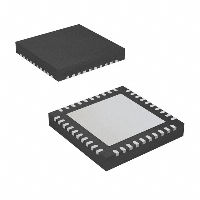


 工商网监
湘ICP备2023018690号
工商网监
湘ICP备2023018690号
