Low Power Wideband Fractional
RF Synthesizer / PLL
Description
Features
The 8V97053L is a high performance Wideband RF Synthesizer /
PLL optimized for use as the local oscillator (LO) in Multi-Carrier,
Multi-mode FDD & TDD Base Station radio card. It is offered in a
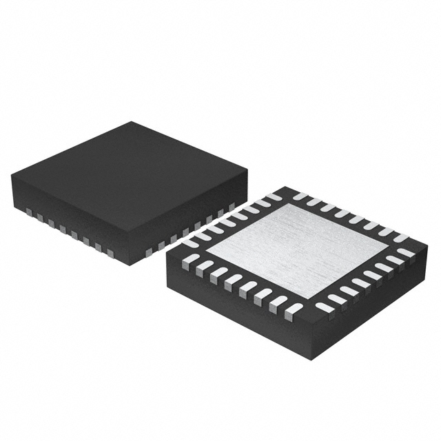
compact 5x5, 32-VFQFN package.
• Dual Differential Outputs
8V97053L
Datasheet
• Output frequency range: 34.375MHz to 4400MHz (continuous
range)
• RF Output Divide by 1, 2, 4, 8, 16, 32, 64
The 8V97053L Wideband RF Synthesizer / PLL offers a default
Fractional Mode with the option to use it with an Integer mode. It
requires an external loop filter.
• Open Drain Outputs (see Output Distribution Section)
• Fractional-N synthesizer (also supports Integer-N mode)
• 16-bit integer and 12-bit fractional
(16-bit fractional when using the extended registers)
The 8V97053L with integrated Voltage Controlled Oscillator (VCO)
supports output frequencies from 34.375MHz to 4400MHz and
maintains superior phase noise and spurious performance.
• 3- or 4-wire SPI interface (compatible with 3.3V and 1.8V)
• Single 3.3V supply
RF_OUT[A:B] output drivers have independently programmable
output power ranging from –4dBm to +7dBm. The RF_OUT outputs
can be muted. The mute function is accessible via a SPI command
or mute pin.
• Logic compatibility: 1.8V
• Integrated high performance low dropout regulators (LDOs) for
excellent power supply noise rejection
• Programmable output power level: -4dBm to +5dBm
(up to +7 when using the extended registers)
The operation of the 8V97053L is controlled by writing to registers
through a 3-wire SPI interface. The 8V97053L also has an additional
option that allows users to read back values from registers by
configuring the MUX_OUT pin as a SDO for the SPI interface. The
SPI interface is compatible with 1.8V logic and tolerant to 3.3V.
• Mute Function
• Ultra low PN for 1.65GHz LO: -142.21dBc/Hz @ 1MHz Offset,
(typical)
In multi-service base stations, very low noise oscillators are required
to generate a large variety of frequencies to the mixers while
maintaining excellent phase noise performance and low power. The
8V97053L offers a large tuning range capable of providing multi-band
local oscillator (LO) frequency synthesis in multi-mode base stations,
thus limiting the use of multiple narrow band RF Synthesizers and
reducing the BOM complexity and cost. The device can operate over
-40°C to +85°C industrial temperature range.
• Lock Detect Indicators
• Input Reference frequency: 5MHz to 310MHz
• 32-Lead, 5x5 VFQFN package
• Automatic VCO band selection (Autocal feature)
• -40°C to +85°C ambient operating temperature
• Lead-free (RoHS 6) packaging
• Supports case temperature 105°C operations
Applications
• Wireless Infrastructure
• Test Equipment
• CATV Equipment
• Military and Aerospace
• Wireless LAN
• Clock Generation
©2018 Integrated Device Technology, Inc.
1
August 9, 2018
�8V97053L Datasheet
Table of Contents
Description . . . . . . . . . . . . . . . . . . . . . . . . . . . . . . . . . . . . . . . . . . . . . . . . . . . . . . . . . . . . . . . . . . . . . . . . . . . . . . . . . . . . . . . . . . . . . . . . . . . .1
Applications . . . . . . . . . . . . . . . . . . . . . . . . . . . . . . . . . . . . . . . . . . . . . . . . . . . . . . . . . . . . . . . . . . . . . . . . . . . . . . . . . . . . . . . . . . . . . . . . . . . .1
Features . . . . . . . . . . . . . . . . . . . . . . . . . . . . . . . . . . . . . . . . . . . . . . . . . . . . . . . . . . . . . . . . . . . . . . . . . . . . . . . . . . . . . . . . . . . . . . . . . . . . . .1
8V97053L Block Diagram . . . . . . . . . . . . . . . . . . . . . . . . . . . . . . . . . . . . . . . . . . . . . . . . . . . . . . . . . . . . . . . . . . . . . . . . . . . . . . . . . . . . . . . . .6
Pin Assignment . . . . . . . . . . . . . . . . . . . . . . . . . . . . . . . . . . . . . . . . . . . . . . . . . . . . . . . . . . . . . . . . . . . . . . . . . . . . . . . . . . . . . . . . . . . . . . . . .6
Pin Description and Characteristic Tables . . . . . . . . . . . . . . . . . . . . . . . . . . . . . . . . . . . . . . . . . . . . . . . . . . . . . . . . . . . . . . . . . . . . . . . . . . . .7
Table 1. Pin Description . . . . . . . . . . . . . . . . . . . . . . . . . . . . . . . . . . . . . . . . . . . . . . . . . . . . . . . . . . . . . . . . . . . . . . . . . . . . . . . . . . . . . . . . .7
Table 2. Pin Characteristics . . . . . . . . . . . . . . . . . . . . . . . . . . . . . . . . . . . . . . . . . . . . . . . . . . . . . . . . . . . . . . . . . . . . . . . . . . . . . . . . . . . . . .8
Table 3. Supply Pins and Associated Current Return Paths . . . . . . . . . . . . . . . . . . . . . . . . . . . . . . . . . . . . . . . . . . . . . . . . . . . . . . . . . . . . .8
Principles of Operation . . . . . . . . . . . . . . . . . . . . . . . . . . . . . . . . . . . . . . . . . . . . . . . . . . . . . . . . . . . . . . . . . . . . . . . . . . . . . . . . . . . . . . . . . . .9
Synthesizer Programming . . . . . . . . . . . . . . . . . . . . . . . . . . . . . . . . . . . . . . . . . . . . . . . . . . . . . . . . . . . . . . . . . . . . . . . . . . . . . . . . . . . . . . 9
Reference Input Stage . . . . . . . . . . . . . . . . . . . . . . . . . . . . . . . . . . . . . . . . . . . . . . . . . . . . . . . . . . . . . . . . . . . . . . . . . . . . . . . . . . . . . . . . .9
Reference Doubler . . . . . . . . . . . . . . . . . . . . . . . . . . . . . . . . . . . . . . . . . . . . . . . . . . . . . . . . . . . . . . . . . . . . . . . . . . . . . . . . . . . . . . . . . . .10
Table 4A. Lock Detect Precision (LDP) . . . . . . . . . . . . . . . . . . . . . . . . . . . . . . . . . . . . . . . . . . . . . . . . . . . . . . . . . . . . . . . . . . . . . . . . . .10
Feedback Divider . . . . . . . . . . . . . . . . . . . . . . . . . . . . . . . . . . . . . . . . . . . . . . . . . . . . . . . . . . . . . . . . . . . . . . . . . . . . . . . . . . . . . . . . . . . .11
Figure 1. RF Feedback N Divider . . . . . . . . . . . . . . . . . . . . . . . . . . . . . . . . . . . . . . . . . . . . . . . . . . . . . . . . . . . . . . . . . . . . . . . . . . . . . . .11
Table 4B. Fractional Spurs Due to the Quantization Noise . . . . . . . . . . . . . . . . . . . . . . . . . . . . . . . . . . . . . . . . . . . . . . . . . . . . . . . . . . .12
Phase and Frequency Detector (PFD) and Charge Pump . . . . . . . . . . . . . . . . . . . . . . . . . . . . . . . . . . . . . . . . . . . . . . . . . . . . . . . . . . . .12
Figure 2. Simplified PFD Circuit using D-type Flip-flop . . . . . . . . . . . . . . . . . . . . . . . . . . . . . . . . . . . . . . . . . . . . . . . . . . . . . . . . . . . . . .12
PFD Frequency . . . . . . . . . . . . . . . . . . . . . . . . . . . . . . . . . . . . . . . . . . . . . . . . . . . . . . . . . . . . . . . . . . . . . . . . . . . . . . . . . . . . . . . . . . . . . .13
External Loop Filter . . . . . . . . . . . . . . . . . . . . . . . . . . . . . . . . . . . . . . . . . . . . . . . . . . . . . . . . . . . . . . . . . . . . . . . . . . . . . . . . . . . . . . . . . . .13
Phase Detector Polarity . . . . . . . . . . . . . . . . . . . . . . . . . . . . . . . . . . . . . . . . . . . . . . . . . . . . . . . . . . . . . . . . . . . . . . . . . . . . . . . . . . . . . . .13
Charge Pump High-Impedance . . . . . . . . . . . . . . . . . . . . . . . . . . . . . . . . . . . . . . . . . . . . . . . . . . . . . . . . . . . . . . . . . . . . . . . . . . . . . . . . .13
Integrated Low Noise VCO . . . . . . . . . . . . . . . . . . . . . . . . . . . . . . . . . . . . . . . . . . . . . . . . . . . . . . . . . . . . . . . . . . . . . . . . . . . . . . . . . . . . .13
Output Distribution Section . . . . . . . . . . . . . . . . . . . . . . . . . . . . . . . . . . . . . . . . . . . . . . . . . . . . . . . . . . . . . . . . . . . . . . . . . . . . . . . . . . . . .14
Figure 3. Output Clock Distribution . . . . . . . . . . . . . . . . . . . . . . . . . . . . . . . . . . . . . . . . . . . . . . . . . . . . . . . . . . . . . . . . . . . . . . . . . . . . . .14
Figure 4. Output Stage . . . . . . . . . . . . . . . . . . . . . . . . . . . . . . . . . . . . . . . . . . . . . . . . . . . . . . . . . . . . . . . . . . . . . . . . . . . . . . . . . . . . . . .14
Output Matching . . . . . . . . . . . . . . . . . . . . . . . . . . . . . . . . . . . . . . . . . . . . . . . . . . . . . . . . . . . . . . . . . . . . . . . . . . . . . . . . . . . . . . . . . . . . .15
Figure 5. Broadband Matching Termination . . . . . . . . . . . . . . . . . . . . . . . . . . . . . . . . . . . . . . . . . . . . . . . . . . . . . . . . . . . . . . . . . . . . . . .15
Figure 6. Optimal Matching Termination . . . . . . . . . . . . . . . . . . . . . . . . . . . . . . . . . . . . . . . . . . . . . . . . . . . . . . . . . . . . . . . . . . . . . . . . . .15
Band Selection Disable . . . . . . . . . . . . . . . . . . . . . . . . . . . . . . . . . . . . . . . . . . . . . . . . . . . . . . . . . . . . . . . . . . . . . . . . . . . . . . . . . . . . . . . .15
Phase Adjust . . . . . . . . . . . . . . . . . . . . . . . . . . . . . . . . . . . . . . . . . . . . . . . . . . . . . . . . . . . . . . . . . . . . . . . . . . . . . . . . . . . . . . . . . . . . . . . .16
Phase Resync . . . . . . . . . . . . . . . . . . . . . . . . . . . . . . . . . . . . . . . . . . . . . . . . . . . . . . . . . . . . . . . . . . . . . . . . . . . . . . . . . . . . . . . . . . . . . . .16
Figure 7. 12-bit Counter for Fast Lock and Phase Resync . . . . . . . . . . . . . . . . . . . . . . . . . . . . . . . . . . . . . . . . . . . . . . . . . . . . . . . . . . . .16
Fast Lock Function . . . . . . . . . . . . . . . . . . . . . . . . . . . . . . . . . . . . . . . . . . . . . . . . . . . . . . . . . . . . . . . . . . . . . . . . . . . . . . . . . . . . . . . . . . .17
Figure 8. Example of Fast Lock Mode Loop Filter Topology . . . . . . . . . . . . . . . . . . . . . . . . . . . . . . . . . . . . . . . . . . . . . . . . . . . . . . . . . .17
RF Output Power . . . . . . . . . . . . . . . . . . . . . . . . . . . . . . . . . . . . . . . . . . . . . . . . . . . . . . . . . . . . . . . . . . . . . . . . . . . . . . . . . . . . . . . . . . . .18
MUX_OUT . . . . . . . . . . . . . . . . . . . . . . . . . . . . . . . . . . . . . . . . . . . . . . . . . . . . . . . . . . . . . . . . . . . . . . . . . . . . . . . . . . . . . . . . . . . . . . . . . .18
Table 4C. MUX_OUT Pin Configuration . . . . . . . . . . . . . . . . . . . . . . . . . . . . . . . . . . . . . . . . . . . . . . . . . . . . . . . . . . . . . . . . . . . . . . . . . .18
Power-Down Mode . . . . . . . . . . . . . . . . . . . . . . . . . . . . . . . . . . . . . . . . . . . . . . . . . . . . . . . . . . . . . . . . . . . . . . . . . . . . . . . . . . . . . . . . . . .18
Default Power-Up Conditions . . . . . . . . . . . . . . . . . . . . . . . . . . . . . . . . . . . . . . . . . . . . . . . . . . . . . . . . . . . . . . . . . . . . . . . . . . . . . . . . . . .19
Program Modes . . . . . . . . . . . . . . . . . . . . . . . . . . . . . . . . . . . . . . . . . . . . . . . . . . . . . . . . . . . . . . . . . . . . . . . . . . . . . . . . . . . . . . . . . . . . . .19
Table 4D. Control Bits Configuration . . . . . . . . . . . . . . . . . . . . . . . . . . . . . . . . . . . . . . . . . . . . . . . . . . . . . . . . . . . . . . . . . . . . . . . . . . . .19
©2018 Integrated Device Technology, Inc.
2
August 9, 2018
�8V97053L Datasheet
Timing Characteristics . . . . . . . . . . . . . . . . . . . . . . . . . . . . . . . . . . . . . . . . . . . . . . . . . . . . . . . . . . . . . . . . . . . . . . . . . . . . . . . . . . . . . . . 20
Figure 9. SPI Write Cycle Timing Diagram . . . . . . . . . . . . . . . . . . . . . . . . . . . . . . . . . . . . . . . . . . . . . . . . . . . . . . . . . . . . . . . . . . . . . . . 20
Figure 10. SPI Read Cycle Timing Diagram . . . . . . . . . . . . . . . . . . . . . . . . . . . . . . . . . . . . . . . . . . . . . . . . . . . . . . . . . . . . . . . . . . . . . . 20
Table 4E. SPI Read / Write Cycle Timing Parameters . . . . . . . . . . . . . . . . . . . . . . . . . . . . . . . . . . . . . . . . . . . . . . . . . . . . . . . . . . . . . . 20
3- or 4-Wire SPI Interface Description . . . . . . . . . . . . . . . . . . . . . . . . . . . . . . . . . . . . . . . . . . . . . . . . . . . . . . . . . . . . . . . . . . . . . . . . . . . 21
Table 4F. SPI Mode Serial Word Structure . . . . . . . . . . . . . . . . . . . . . . . . . . . . . . . . . . . . . . . . . . . . . . . . . . . . . . . . . . . . . . . . . . . . . . . 21
Register Map . . . . . . . . . . . . . . . . . . . . . . . . . . . . . . . . . . . . . . . . . . . . . . . . . . . . . . . . . . . . . . . . . . . . . . . . . . . . . . . . . . . . . . . . . . . . . . . . . 22
Register 0 . . . . . . . . . . . . . . . . . . . . . . . . . . . . . . . . . . . . . . . . . . . . . . . . . . . . . . . . . . . . . . . . . . . . . . . . . . . . . . . . . . . . . . . . . . . . . . . . . 22
Table 5A. Register 0 Bit Allocation . . . . . . . . . . . . . . . . . . . . . . . . . . . . . . . . . . . . . . . . . . . . . . . . . . . . . . . . . . . . . . . . . . . . . . . . . . . . . 22
Table 5B. Register 0: 16-Bit Feedback Divider Integer Value (INT). Function Description . . . . . . . . . . . . . . . . . . . . . . . . . . . . . . . . . . . 22
Table 5C. Register 0: 12-Bit Feedback Divider Fractional Value (FRAC). Function Description . . . . . . . . . . . . . . . . . . . . . . . . . . . . . . 22
Table 5D. Register 0: 3-Bit Control Bits. Function Description . . . . . . . . . . . . . . . . . . . . . . . . . . . . . . . . . . . . . . . . . . . . . . . . . . . . . . . . 23
Register 1 . . . . . . . . . . . . . . . . . . . . . . . . . . . . . . . . . . . . . . . . . . . . . . . . . . . . . . . . . . . . . . . . . . . . . . . . . . . . . . . . . . . . . . . . . . . . . . . . . 24
Table 6A. Register 1 Bit Allocation . . . . . . . . . . . . . . . . . . . . . . . . . . . . . . . . . . . . . . . . . . . . . . . . . . . . . . . . . . . . . . . . . . . . . . . . . . . . . 24
Table 6B. Register 1: 1-Bit BAND_SEL_DISABLE. Function Description . . . . . . . . . . . . . . . . . . . . . . . . . . . . . . . . . . . . . . . . . . . . . . . 24
Table 6C. Register 1: 12-Bit Phase Value (PHASE). Function Description . . . . . . . . . . . . . . . . . . . . . . . . . . . . . . . . . . . . . . . . . . . . . . 24
Table 6D. Register 1: 12-Bit Modulus Value (MOD). Function Description . . . . . . . . . . . . . . . . . . . . . . . . . . . . . . . . . . . . . . . . . . . . . . 25
Table 6E. Register 1: 3-Bit Control Bits. Function Description . . . . . . . . . . . . . . . . . . . . . . . . . . . . . . . . . . . . . . . . . . . . . . . . . . . . . . . . 25
Register 2 . . . . . . . . . . . . . . . . . . . . . . . . . . . . . . . . . . . . . . . . . . . . . . . . . . . . . . . . . . . . . . . . . . . . . . . . . . . . . . . . . . . . . . . . . . . . . . . . . 26
Table 7A. Register 2 Bit Allocation . . . . . . . . . . . . . . . . . . . . . . . . . . . . . . . . . . . . . . . . . . . . . . . . . . . . . . . . . . . . . . . . . . . . . . . . . . . . . 26
Table 7B. Register 2: 2-Bit NOISE MODE. Function Description . . . . . . . . . . . . . . . . . . . . . . . . . . . . . . . . . . . . . . . . . . . . . . . . . . . . . . 26
Table 7C. Register 2: 3-Bit MUX_OUT. Function Description . . . . . . . . . . . . . . . . . . . . . . . . . . . . . . . . . . . . . . . . . . . . . . . . . . . . . . . . . 26
Table 7D. Register 2: 1-Bit REF DOUBLER. Function Description . . . . . . . . . . . . . . . . . . . . . . . . . . . . . . . . . . . . . . . . . . . . . . . . . . . . 27
Table 7E. Register 2: 1-Bit REF DIV2. Function Description . . . . . . . . . . . . . . . . . . . . . . . . . . . . . . . . . . . . . . . . . . . . . . . . . . . . . . . . . 27
Table 7F. Register 2: 10-Bit R COUNTER (R). Function Description . . . . . . . . . . . . . . . . . . . . . . . . . . . . . . . . . . . . . . . . . . . . . . . . . . . 27
Table 7G. Register 2: 1-Bit DOUBLE BUFFER. Function Description . . . . . . . . . . . . . . . . . . . . . . . . . . . . . . . . . . . . . . . . . . . . . . . . . . 27
Table 7H. Register 2: 4-Bit Charge Pump Setting (ICP SETTING). Function Description . . . . . . . . . . . . . . . . . . . . . . . . . . . . . . . . . . . 28
Table 7I. Register 2: 1-Bit Lock Detect Function (LDF). Function Description . . . . . . . . . . . . . . . . . . . . . . . . . . . . . . . . . . . . . . . . . . . . 28
Table 7J. Register 2: 1-Bit Lock Detect Precision. Function Description . . . . . . . . . . . . . . . . . . . . . . . . . . . . . . . . . . . . . . . . . . . . . . . . 28
Table 7K. Register 2: 1-Bit Phase Detector Polarity. Function Description . . . . . . . . . . . . . . . . . . . . . . . . . . . . . . . . . . . . . . . . . . . . . . 28
Table 7L. Register 2: 1-Bit Power Down. Function Description . . . . . . . . . . . . . . . . . . . . . . . . . . . . . . . . . . . . . . . . . . . . . . . . . . . . . . . 29
Table 7M. Register 2: 1-Bit Charge Pump High-Impedance. Function Description . . . . . . . . . . . . . . . . . . . . . . . . . . . . . . . . . . . . . . . . 29
Table 7N. Register 2: 3-Bit Control Bits. Function Description . . . . . . . . . . . . . . . . . . . . . . . . . . . . . . . . . . . . . . . . . . . . . . . . . . . . . . . . 29
Register 3 . . . . . . . . . . . . . . . . . . . . . . . . . . . . . . . . . . . . . . . . . . . . . . . . . . . . . . . . . . . . . . . . . . . . . . . . . . . . . . . . . . . . . . . . . . . . . . . . . 30
Table 8A. Register 3 Bit Allocation . . . . . . . . . . . . . . . . . . . . . . . . . . . . . . . . . . . . . . . . . . . . . . . . . . . . . . . . . . . . . . . . . . . . . . . . . . . . . 30
Table 8B. Register 3: 1-Bit Band Select Clock Mode. Function Description . . . . . . . . . . . . . . . . . . . . . . . . . . . . . . . . . . . . . . . . . . . . . . 30
Table 8C. Register 3: 2-Bit Clock Divider Mode. Function Description . . . . . . . . . . . . . . . . . . . . . . . . . . . . . . . . . . . . . . . . . . . . . . . . . . 30
Table 8D. Register 3: 12-Bit Clock Divider Value (CLKDIV). Function Description . . . . . . . . . . . . . . . . . . . . . . . . . . . . . . . . . . . . . . . . 30
Table 8E. Register 3: 3-Bit Control Bits. Function Description . . . . . . . . . . . . . . . . . . . . . . . . . . . . . . . . . . . . . . . . . . . . . . . . . . . . . . . . 31
Register 4 . . . . . . . . . . . . . . . . . . . . . . . . . . . . . . . . . . . . . . . . . . . . . . . . . . . . . . . . . . . . . . . . . . . . . . . . . . . . . . . . . . . . . . . . . . . . . . . . . 32
Table 9A. Register 4 Bit Allocation . . . . . . . . . . . . . . . . . . . . . . . . . . . . . . . . . . . . . . . . . . . . . . . . . . . . . . . . . . . . . . . . . . . . . . . . . . . . . 32
Table 9B. Register 4: 1-Bit Feedback Select. Function Description . . . . . . . . . . . . . . . . . . . . . . . . . . . . . . . . . . . . . . . . . . . . . . . . . . . . 32
Table 9C. Register 4: 3-Bit RF Output Divider (÷ MO) Select. Function Description . . . . . . . . . . . . . . . . . . . . . . . . . . . . . . . . . . . . . . . 32
Table 9D. Register 4: 8-Bit Band Select Clock Counter. Function Description . . . . . . . . . . . . . . . . . . . . . . . . . . . . . . . . . . . . . . . . . . . . 33
Table 9E. Register 4: 1-Bit VCO Power Down. Function Description . . . . . . . . . . . . . . . . . . . . . . . . . . . . . . . . . . . . . . . . . . . . . . . . . . . 33
Table 9F. Register 4: 1-Bit Mute Till Lock Detect. Function Description . . . . . . . . . . . . . . . . . . . . . . . . . . . . . . . . . . . . . . . . . . . . . . . . . 33
Table 9G. Register 4: 1-Bit RF_OUTB Select. Function Description . . . . . . . . . . . . . . . . . . . . . . . . . . . . . . . . . . . . . . . . . . . . . . . . . . . 33
©2018 Integrated Device Technology, Inc.
3
August 9, 2018
�8V97053L Datasheet
Table 9H. Register 4: 1-Bit RF_OUTB Enable. Function Description . . . . . . . . . . . . . . . . . . . . . . . . . . . . . . . . . . . . . . . . . . . . . . . . . . . .33
Table 9I. Register 4: 1-Bit RF_OUTA Enable. Function Description . . . . . . . . . . . . . . . . . . . . . . . . . . . . . . . . . . . . . . . . . . . . . . . . . . . . .33
Table 9I. Register 4: 1-Bit RF_OUTA Enable. Function Description . . . . . . . . . . . . . . . . . . . . . . . . . . . . . . . . . . . . . . . . . . . . . . . . . . . . .33
Table 9J. Register 4: 2-Bit RF_OUTA Output Power. Function Description . . . . . . . . . . . . . . . . . . . . . . . . . . . . . . . . . . . . . . . . . . . . . . .34
Table 9K. Register 4: 3-Bit Control Bits. Function Description . . . . . . . . . . . . . . . . . . . . . . . . . . . . . . . . . . . . . . . . . . . . . . . . . . . . . . . . .34
Register 5 . . . . . . . . . . . . . . . . . . . . . . . . . . . . . . . . . . . . . . . . . . . . . . . . . . . . . . . . . . . . . . . . . . . . . . . . . . . . . . . . . . . . . . . . . . . . . . . . . .35
Table 10A. Register 5 Bit Allocation . . . . . . . . . . . . . . . . . . . . . . . . . . . . . . . . . . . . . . . . . . . . . . . . . . . . . . . . . . . . . . . . . . . . . . . . . . . . .35
Table 10B. Register 5: 2-Bit LD (Lock Detect) Pin Mode. Function Description . . . . . . . . . . . . . . . . . . . . . . . . . . . . . . . . . . . . . . . . . . . .35
Table 10C. Register 5: 3-Bit Control Bits. Function Description . . . . . . . . . . . . . . . . . . . . . . . . . . . . . . . . . . . . . . . . . . . . . . . . . . . . . . . .35
Extended Registers, (Registers 6 and 7) . . . . . . . . . . . . . . . . . . . . . . . . . . . . . . . . . . . . . . . . . . . . . . . . . . . . . . . . . . . . . . . . . . . . . . . . . .36
Register 6 . . . . . . . . . . . . . . . . . . . . . . . . . . . . . . . . . . . . . . . . . . . . . . . . . . . . . . . . . . . . . . . . . . . . . . . . . . . . . . . . . . . . . . . . . . . . . . . . . .36
Table 11A. Register 6 Bit Allocation
. . . . . . . . . . . . . . . . . . . . . . . . . . . . . . . . . . . . . . . . . . . . . . . . . . . . . . . . . . . . . . . . . . . . . . . . . . . .36
Table 11B. Register 6: 1-Bit Digital Lock Detect. Function Description . . . . . . . . . . . . . . . . . . . . . . . . . . . . . . . . . . . . . . . . . . . . . . . . . .36
Table 11C. Register 6: 1-Bit Band Select Status (Read Only). Function Description . . . . . . . . . . . . . . . . . . . . . . . . . . . . . . . . . . . . . . . .36
Table 11D. Register 6: 2-Bit Extra Lock Detect Precision. Function Description . . . . . . . . . . . . . . . . . . . . . . . . . . . . . . . . . . . . . . . . . . .37
Table 11E. Register 6: 1-Bit Extra Bit of RF_OUTB Power. Function Description . . . . . . . . . . . . . . . . . . . . . . . . . . . . . . . . . . . . . . . . . .37
Table 11F. Register 6: 1-Bit Extra Bit of RF_OUTA Power. Function Description . . . . . . . . . . . . . . . . . . . . . . . . . . . . . . . . . . . . . . . . . . .38
Table 11G. Register 6: 2-Bit Sigma Delta Modulator Order Configuration. Function Description . . . . . . . . . . . . . . . . . . . . . . . . . . . . . . .38
Table 11H. Register 6: 2-Bit Dither Gain Configuration. Function Description . . . . . . . . . . . . . . . . . . . . . . . . . . . . . . . . . . . . . . . . . . . . .38
Table 11I. Register 6: 1-Bit Dither Noise Shaping Configuration. Function Description . . . . . . . . . . . . . . . . . . . . . . . . . . . . . . . . . . . . . .38
Table 11J. Register 6: 1-Bit Sigma Delta Modulator Type Configuration. Function Description . . . . . . . . . . . . . . . . . . . . . . . . . . . . . . . .38
Table 11K. Register 6: 2-Bit VCO Band Selection Accuracy Configuration. Function Description . . . . . . . . . . . . . . . . . . . . . . . . . . . . . .39
Table 11N. Register 6: 4-Bit Extra Most Significant Bits of Band Select Divider. Function Description
. . . . . . . . . . . . . . . . . . . . . . . . .39
Table 11O. Register 6: 3-Bit Control Bits. Function Description . . . . . . . . . . . . . . . . . . . . . . . . . . . . . . . . . . . . . . . . . . . . . . . . . . . . . . . .39
Register 7 . . . . . . . . . . . . . . . . . . . . . . . . . . . . . . . . . . . . . . . . . . . . . . . . . . . . . . . . . . . . . . . . . . . . . . . . . . . . . . . . . . . . . . . . . . . . . . . . . .40
Table 12A. Register 7 Bit Allocation. . . . . . . . . . . . . . . . . . . . . . . . . . . . . . . . . . . . . . . . . . . . . . . . . . . . . . . . . . . . . . . . . . . . . . . . . . . . . .40
Table 12B. Register 7: 1-Bit Loss of Digital Lock. Function Description . . . . . . . . . . . . . . . . . . . . . . . . . . . . . . . . . . . . . . . . . . . . . . . . . .40
Table 12C. Register 7: 1-Bit Loss of Analog Lock. Function Description . . . . . . . . . . . . . . . . . . . . . . . . . . . . . . . . . . . . . . . . . . . . . . . . .40
Table 12D. Register 7: 1-Bit SPI Error. Function Description . . . . . . . . . . . . . . . . . . . . . . . . . . . . . . . . . . . . . . . . . . . . . . . . . . . . . . . . . .40
Table 12E. Register 7: 3-Bit Revision ID. Function Description . . . . . . . . . . . . . . . . . . . . . . . . . . . . . . . . . . . . . . . . . . . . . . . . . . . . . . . .41
Table 12F. Register 7: 4-Bit Device ID. Function Description . . . . . . . . . . . . . . . . . . . . . . . . . . . . . . . . . . . . . . . . . . . . . . . . . . . . . . . . . .41
Table 12G. Register 7: 1-Bit Resolution Select. Function Description. . . . . . . . . . . . . . . . . . . . . . . . . . . . . . . . . . . . . . . . . . . . . . . . . . . .41
Table 12J. Register 7: 4-Bit Extra Bits of MOD Value. Function Description. . . . . . . . . . . . . . . . . . . . . . . . . . . . . . . . . . . . . . . . . . . . . . .42
Table 12K. Register 7: 4-Bit Extra Bits of FRAC Value. Function Description. . . . . . . . . . . . . . . . . . . . . . . . . . . . . . . . . . . . . . . . . . . . . .42
Table 12L. Register 7: 1-Bit SCLKE. Function Description . . . . . . . . . . . . . . . . . . . . . . . . . . . . . . . . . . . . . . . . . . . . . . . . . . . . . . . . . . . .43
Table 12M. Register 7: 1-Bit READBACK_ADDR. Function Description . . . . . . . . . . . . . . . . . . . . . . . . . . . . . . . . . . . . . . . . . . . . . . . . .43
Table 12N. Register 7: 1-Bit SPI_R_WN. Function Description . . . . . . . . . . . . . . . . . . . . . . . . . . . . . . . . . . . . . . . . . . . . . . . . . . . . . . . .43
Table 12O. Register 7: 3-Bit Control Bits. Function Description . . . . . . . . . . . . . . . . . . . . . . . . . . . . . . . . . . . . . . . . . . . . . . . . . . . . . . . .43
Absolute Maximum Ratings . . . . . . . . . . . . . . . . . . . . . . . . . . . . . . . . . . . . . . . . . . . . . . . . . . . . . . . . . . . . . . . . . . . . . . . . . . . . . . . . . . . . . .44
Table 13. Absolute Maximum Ratings . . . . . . . . . . . . . . . . . . . . . . . . . . . . . . . . . . . . . . . . . . . . . . . . . . . . . . . . . . . . . . . . . . . . . . . . . . . . .44
DC Electrical Characteristics . . . . . . . . . . . . . . . . . . . . . . . . . . . . . . . . . . . . . . . . . . . . . . . . . . . . . . . . . . . . . . . . . . . . . . . . . . . . . . . . . . . . .45
Table 14A. Power Supply DC Characteristics, VDDX = VDDA = 3.3V ± 5%, TA = -40°C to +85°C . . . . . . . . . . . . . . . . . . . . . . . . . . . . . . . .45
Table 14B. Output Divider Incremental Current . . . . . . . . . . . . . . . . . . . . . . . . . . . . . . . . . . . . . . . . . . . . . . . . . . . . . . . . . . . . . . . . . . . . . .45
Table 14C. Typical Current by Power Domain . . . . . . . . . . . . . . . . . . . . . . . . . . . . . . . . . . . . . . . . . . . . . . . . . . . . . . . . . . . . . . . . . . . . . . .46
Table 14D. LVCMOS DC Characteristics, VDDX = VDDA = 3.3V ± 5%, TA = -40°C to 85°C . . . . . . . . . . . . . . . . . . . . . . . . . . . . . . . . . . . . .46
©2018 Integrated Device Technology, Inc.
4
August 9, 2018
�8V97053L Datasheet
AC Electrical Characteristics . . . . . . . . . . . . . . . . . . . . . . . . . . . . . . . . . . . . . . . . . . . . . . . . . . . . . . . . . . . . . . . . . . . . . . . . . . . . . . . . . . . . .47
Table 15A. AC Characteristics, VDDX = VDDA = 3.3V ± 5%, TA = -40°C to 85°C. . . . . . . . . . . . . . . . . . . . . . . . . . . . . . . . . . . . . . . . . . . . . .47
Table 15B. RF_OUT[A:B] Phase Noise and Jitter Characteristics, VDDX = VDDA = 3.3V ± 5%, TA = -40°C to 85°C . . . . . . . . . . . . . . . . .48
Phase Noise (Closed-Loop) at 156.25MHz (3.3V). . . . . . . . . . . . . . . . . . . . . . . . . . . . . . . . . . . . . . . . . . . . . . . . . . . . . . . . . . . . . . . . . . . . .50
Phase Noise (Closed-Loop) at 1.76GHz (3.3V) . . . . . . . . . . . . . . . . . . . . . . . . . . . . . . . . . . . . . . . . . . . . . . . . . . . . . . . . . . . . . . . . . . . . . . .50
Phase Noise (Closed-Loop) at 2.05GHz (3.3V) . . . . . . . . . . . . . . . . . . . . . . . . . . . . . . . . . . . . . . . . . . . . . . . . . . . . . . . . . . . . . . . . . . . . . . .51
Phase Noise (Open-Loop) at 745MHz (3.3V) . . . . . . . . . . . . . . . . . . . . . . . . . . . . . . . . . . . . . . . . . . . . . . . . . . . . . . . . . . . . . . . . . . . . . . . .51
Phase Noise Performance (Open-Loop) at 1.1GHz (3.3V) . . . . . . . . . . . . . . . . . . . . . . . . . . . . . . . . . . . . . . . . . . . . . . . . . . . . . . . . . . . . . .52
Phase Noise Performance (Open-Loop) at 1.65GHz (3.3V) . . . . . . . . . . . . . . . . . . . . . . . . . . . . . . . . . . . . . . . . . . . . . . . . . . . . . . . . . . . . .52
Phase Noise Performance (Open-Loop) at 2.3GHz (3.3V) . . . . . . . . . . . . . . . . . . . . . . . . . . . . . . . . . . . . . . . . . . . . . . . . . . . . . . . . . . . . . .53
Phase Noise Performance (Open-Loop) at 3.8GHz (3.3V) . . . . . . . . . . . . . . . . . . . . . . . . . . . . . . . . . . . . . . . . . . . . . . . . . . . . . . . . . . . . . .53
Phase Noise Performance (Open-Loop) at 4.4GHz (3.3V) . . . . . . . . . . . . . . . . . . . . . . . . . . . . . . . . . . . . . . . . . . . . . . . . . . . . . . . . . . . . . .54
Applications Information . . . . . . . . . . . . . . . . . . . . . . . . . . . . . . . . . . . . . . . . . . . . . . . . . . . . . . . . . . . . . . . . . . . . . . . . . . . . . . . . . . . . . . . . .55
Loop Filter Calculations . . . . . . . . . . . . . . . . . . . . . . . . . . . . . . . . . . . . . . . . . . . . . . . . . . . . . . . . . . . . . . . . . . . . . . . . . . . . . . . . . . . . . . .55
2nd Order Loop Filter . . . . . . . . . . . . . . . . . . . . . . . . . . . . . . . . . . . . . . . . . . . . . . . . . . . . . . . . . . . . . . . . . . . . . . . . . . . . . . . . . . . . . . .55
Figure 11. Typical 2nd Order Loop Filter . . . . . . . . . . . . . . . . . . . . . . . . . . . . . . . . . . . . . . . . . . . . . . . . . . . . . . . . . . . . . . . . . . . . . . . .55
3rd Order Loop Filter . . . . . . . . . . . . . . . . . . . . . . . . . . . . . . . . . . . . . . . . . . . . . . . . . . . . . . . . . . . . . . . . . . . . . . . . . . . . . . . . . . . . . . . 57
Figure 12. Typical 3rd Order Loop Filter . . . . . . . . . . . . . . . . . . . . . . . . . . . . . . . . . . . . . . . . . . . . . . . . . . . . . . . . . . . . . . . . . . . . . . . .57
Recommendations for Unused Input and Output Pins . . . . . . . . . . . . . . . . . . . . . . . . . . . . . . . . . . . . . . . . . . . . . . . . . . . . . . . . . . . . . . . .57
Schematic Example . . . . . . . . . . . . . . . . . . . . . . . . . . . . . . . . . . . . . . . . . . . . . . . . . . . . . . . . . . . . . . . . . . . . . . . . . . . . . . . . . . . . . . . . . .58
Figure 13A. An 8V97053L General Application Schematic Example . . . . . . . . . . . . . . . . . . . . . . . . . . . . . . . . . . . . . . . . . . . . . . . . . . . .59
Figure 13B. Schematic Example for Driving Single Ended Mixer . . . . . . . . . . . . . . . . . . . . . . . . . . . . . . . . . . . . . . . . . . . . . . . . . . . . . . .60
Power Considerations . . . . . . . . . . . . . . . . . . . . . . . . . . . . . . . . . . . . . . . . . . . . . . . . . . . . . . . . . . . . . . . . . . . . . . . . . . . . . . . . . . . . . . . . . . .61
Table 16. Thermal Resistance JA for 32 Lead VFQFN, Forced Convection . . . . . . . . . . . . . . . . . . . . . . . . . . . . . . . . . . . . . . . . . . . . . .61
Example 2: VCO Frequency Range = 2590MHz to 3624MHz . . . . . . . . . . . . . . . . . . . . . . . . . . . . . . . . . . . . . . . . . . . . . . . . . . . . . . . .62
Reliability Information . . . . . . . . . . . . . . . . . . . . . . . . . . . . . . . . . . . . . . . . . . . . . . . . . . . . . . . . . . . . . . . . . . . . . . . . . . . . . . . . . . . . . . . . . . .63
Table 17A. JA vs. Air Flow Table for a 32 lead VFQFN . . . . . . . . . . . . . . . . . . . . . . . . . . . . . . . . . . . . . . . . . . . . . . . . . . . . . . . . . . . . . . . .63
Table 17B. JB vs. Air Flow Table for a 32 lead VFQFN . . . . . . . . . . . . . . . . . . . . . . . . . . . . . . . . . . . . . . . . . . . . . . . . . . . . . . . . . . . . . . . .63
Package Outline Drawings . . . . . . . . . . . . . . . . . . . . . . . . . . . . . . . . . . . . . . . . . . . . . . . . . . . . . . . . . . . . . . . . . . . . . . . . . . . . . . . . . . . . . . .63
Ordering Information . . . . . . . . . . . . . . . . . . . . . . . . . . . . . . . . . . . . . . . . . . . . . . . . . . . . . . . . . . . . . . . . . . . . . . . . . . . . . . . . . . . . . . . . . . . .63
Table 18. Ordering Information . . . . . . . . . . . . . . . . . . . . . . . . . . . . . . . . . . . . . . . . . . . . . . . . . . . . . . . . . . . . . . . . . . . . . . . . . . . . . . . . . .63
Table 19. Pin 1 Orientation in Tape and Reel Packaging . . . . . . . . . . . . . . . . . . . . . . . . . . . . . . . . . . . . . . . . . . . . . . . . . . . . . . . . . . . . . . .64
Contact Information . . . . . . . . . . . . . . . . . . . . . . . . . . . . . . . . . . . . . . . . . . . . . . . . . . . . . . . . . . . . . . . . . . . . . . . . . . . . . . . . . . . . . . . . . . . . .68
©2018 Integrated Device Technology, Inc.
5
August 9, 2018
�8V97053L Datasheet
8V97053L Block Diagram
SDO
MUX_OUT
Lock
Detect
x2
REF_IN
CP_OUT
Charge
Pump
PFD
÷2
÷R
LD
External
Loop
Filter
VTUNE
`
16/12 or 16/
16 bit Frac-N
Divider
SCLK
SDI
nCS
FLSW
SPI
÷M0
RF_OUTA
nRF_OUTA
Logic & Registers
CE
RF_OUTB
nRF_OUTB
MUTE
NOTE: 16-Bit Integer / 16-Bit Fractional feedback divider is available when using extended register.
VDD_SD
GND_SD
MUX_OUT
REF_IN
VDDD
GNDD
MUTE
LD
Pin Assignment
32
31
30
29
28
27
26
25
SCLK
1
24
VREF
SDI
2
23
VCOM
nCS
3
22
RCP
CE
4
21
GNDA_VCO
FLSW
5
20
VTUNE
V_CP
6
19
VBIAS
CP_OUT
7
18
GNDA_VCO
GND_CP
8
17
VVCO
10
11
12
13
14
15
16
GNDA_VCO
RF_OUTA
nRF_OUTA
RF_OUTB
nRF_OUTB
VVCO
GNDA
9
VDDA
8V97053L
32-Lead 5mm x 5mm VFQFN
©2018 Integrated Device Technology, Inc.
6
August 9, 2018
�8V97053L Datasheet
Pin Description and Characteristic Tables
Table 1. Pin Description1
Pin
Name
Type
Description
1
SCLK
LVCMOS Input
Pulldown
Serial Clock Input. High-Impedance CMOS input. 1.8V logic. 3.3V tolerant.
2
SDI
LVCMOS Input
Pullup
Serial Data Input. High-Impedance CMOS input. 1.8V logic. 3.3V tolerant.
3
nCS
LVCMOS Input
Pulldown
4
CE
LVCMOS Input
Pullup
5
FLSW
Analog
Fast Lock Switch. A connection should be made from the loop filter to this pin
when using the fast lock mode.
6
V_CP
Power
Charge Pump Power Supply. V_CP must have the same value as VDDA. Place
decoupling capacitors to the ground plane as close to this pin as possible.
7
CP_OUT
Analog
Charge Pump Output. When enabled, this output provides ±ICP to the
external loop filter. The output of the loop filter is connected to VTUNE to drive
the internal VCO.
8
GND_CP
Ground
Charge Pump Power Supply Ground.
9
GNDA
Ground
Analog Power Supply Ground.
10
VDDA
Power
Analog Supply. This pin ranges from 3.3V ± 5%. VDDA must have the same
value as VDDD.
11
GNDA_VCO
Ground
VCO Analog Power Supply Ground.
12
RF_OUTA
Output
Clock Output pair A. The output level is programmable.
13
nRF_OUTA
Output
Clock Output pair A. The output level is programmable.
14
RF_OUTB
Output
Clock Output pair B. The output level is programmable.
15
nRF_OUTB
Output
Clock Output pair B. The output level is programmable.
16
VVCO
Power
VCO Supply. This pin ranges from 3.3V ± 5%. VVCO must have the same
value as VDDA.
17
VVCO
Power
VCO Supply. This pin ranges from 3.3V ± 5%. VVCO must have the same
value as VDDA.
18
GNDA_VCO
Ground
VCO Analog Power Supply Ground.
19
VBIAS
Analog
Place decoupling capacitors (10µF) to ground, as close to this pin as possible.
20
VTUNE
21
GNDA_VCO
Ground
VCO Analog Power Supply Ground.
22
RCP
Analog
Sets the charge pump current. Requires external resistor.
23
VCOM
Analog
Place decoupling capacitors (1µF – 10µF) to ground, as close to this pin as
possible.
24
VREF
Analog
Place decoupling capacitors (10µF) to ground, as close to this pin as possible.
25
LD
26
MUTE
LVCMOS Input
27
GNDD
Ground
Load Enable. High-Impedance CMOS input. 1.8V logic. 3.3V tolerant. Active
Low.
Chip Enable. On logic Low, powers down the device and puts the charge
pump into High-Impedance mode. Powers up the device on logic High.
Control Input to tune the VCO.
Lock Detect. Logic High indicates PLL lock. Logic Low indicates loss of PLL
lock.
LVCMOS Output
©2018 Integrated Device Technology, Inc.
Pullup
RF_OUTA and RF_OUTB Power-Down. A logic low on this pin mutes the
RF_OUT outputs and puts them in High-Impedance.
Digital Power Supply Ground.
7
August 9, 2018
�8V97053L Datasheet
Table 1. Pin Description1 (Continued)
28
VDDD
Power
Digital Supply. VDDD must have the same value as VDDA.
29
REF_IN
30
MUX_OUT
31
GND_SD
Ground
Digital Sigma Delta Modulator Power Supply Ground.
32
VDD_SD
Power
Digital Sigma Delta Modulator Supply. VDD_SD must have the same value as
VDDA.
EP
Exposed Pad
Ground
Must be connected to GND.
LVCMOS Input
Reference Input. This CMOS input has a nominal threshold of VDDA/2 and a
DC equivalent input resistance of 100k. This input can be driven from a TTL
or CMOS crystal oscillator, or it can be AC-coupled.
Analog
LVCMOS Output
Multiplexed Output and Serial Data Out. Refer to Table 4C, Page 18.
NOTE 1. Pullup and Pulldown refer to internal input resistors. See Table 2, Pin Characteristics, for typical values.
Table 2. Pin Characteristics
Symbol
Parameter
Test Conditions
Cin
Input Capacitance
ROUT
LVCMOS Output Impedance
RPULLUP
RPULLDOWN
Minimum
Typical
Maximum
Units
4
pF
38
Input Pullup Resistor
51
k
Input Pulldown Resistor
51
k
MUX_OUT & LD
Table 3. Supply Pins and Associated Current Return Paths
Power Supply Pin Number
Power Supply Pin Name
Associated Ground Pin Number
Associated Ground Pin Name
10
VDDA
9
GNDA
28
VDDD
27
GNDD
32
VDD_SD
31
GND_SD
16, 17
VVCO
11, 18, 21
GNDA_VCO
6
V_CP
8
GND_CP
©2018 Integrated Device Technology, Inc.
8
August 9, 2018
�8V97053L Datasheet
Principles of Operation
Synthesizer Programming
The Fractional-N architecture is implemented via a cascaded programmable dual modulus prescaler. The N divider offers a division ratio in the
feedback path of the PLL, and is given by programming the value of INT, FRAC and MOD in the following equation:
N = INT + FRAC/MOD
(1)
INT is the divide ratio of the binary 16-bits counter (refer to Table 5B, Page 22).
FRAC is the numerator value of the fractional divide ratio. It is programmable from 0 to (MOD – 1). Refer to Table 5C when in 12-bit mode, or
Table 12K when in 16-bit mode.
MOD is the 12-bit or 16-bit modulus. It is programmable from 2 to 4095 in 12-bit mode, and 2 to 65535 in 16-bit mode. Refer to Table 6D when
in 12-bit mode, or Table 12J when in 16-bit mode.
The VCO frequency (fVCO) at RF_OUTA or RF_OUTB is given by the following equation:
fVCO = fPFD x (INT + FRAC/MOD)
(2)
fPFD is the frequency at the input of the Phase and Frequency Detector (PFD).
The 8V97053L offers an Integer mode. To enable that mode, the user has to program the FRAC value to 0.
The device’s VCO features three VCO band-splits to cover the entire range with sufficient margin for process, voltage, and temperature
variations. These are automatically selected by invoking the Autocal feature. The charge pump current is also programmable via the ICP
SETTING register for maximum flexibility.
Via Register 4, one can enable RF_OUTA or both outputs. Similarly, one can disable RF_OUTB or both outputs.
Reference Input Stage
The 8V97053L features one single-ended reference clock input (REF_IN). This single-ended input can be driven by an ac-coupled sine wave
or square wave.
In Power Down mode this input is set to High-Impedance to prevent loading of the reference source.The reference input signal path also
includes an optional doubler.
©2018 Integrated Device Technology, Inc.
9
August 9, 2018
�8V97053L Datasheet
Reference Doubler
To improve the phase noise performance of the device, the reference doubler can be used. By using the doubler, the PFD frequency is also
doubled and the phase noise performance typically improves by 3dB. When operating the device in Fractional mode, the speed of the Sigma
Delta modulator of the N counter is limited to 125MHz, which is also the maximum PFD frequency that can be used in the fractional mode.
When the part operates in Integer-N mode, the PFD frequency is limited to 310MHz.
The user has the possibility to select a higher PFD frequency (up to 310MHz in Integer mode) by doing the following steps using the extended
registers (Register 6 and 7):
1. The user needs to increase the size of the Band Select Clock Divider (normally 8-bits) by setting the bit [D6:D3] in the Register 6 to divide
down to a frequency lower than 500kHz and higher than 125kHz.
2. Use the Bit[D27:D26] to increase the lock detect precision for the faster PFD frequency.
The Lock Detect window should be set as large as possible but less than a period of the phase detector. The phase detector frequency should
be greater than 500kHz.
Table 4A. Lock Detect Precision (LDP)
LDP_Ext2
(D27 of Register 6)
LDP_Ext1
(D26 of Register 6)
LDP
(D7 of Register 2)
LDP value (ns)
0
0
0
10
0
0
1
6
Use of Extended Register 6
0
1
0
3
0
1
1
3
1
0
0
4
1
0
1
4.5
1
1
0
1.5
1
1
1
1.5
©2018 Integrated Device Technology, Inc.
10
August 9, 2018
�8V97053L Datasheet
Feedback Divider
The feedback divider N supports fractional division capability in the PLL feedback path. It consists in an integer N divider of 16-bits, and a
Fractional divider of 12-bits (FRAC) over 12-bits (MOD). FRAC and MOD can be extended to 16-bits when using extended registers.
To select an integer mode only, the user sets FRAC to 0.
FROM VCO OUTPOUT
or FROM M0 OUTPUT
TO PFD
N counter
rd
3 Order
ΣΔ Modulator
12 Bit FRAC
16 Bit INT
+
12 Bit MOD
Figure 1. RF Feedback N Divider
The 16 INT bits (Bit[D30:D15] in Register 0) set the integer part of the feedback division ratio.
The 12 FRAC bits (Bit[D14:D3] in Register 0) set the numerator of the fraction that goes into the Sigma Delta modulator. FRAC can be extended
to 16-bits using the EXT_FRAC bits in Register 7.
The 12 MOD bits (Bit[D14:D3] in Register 1) set the denominator of the fraction that goes into the Sigma Delta modulator. MOD can be
extended to 16-bits using the EXT_MOD bits in Register 7.
From the relation (2), the VCO minimum step frequency is determined by (1/MOD) * fPFD.
FRAC values from 0 to (MOD – 1) cover channels over a frequency range equal to the PFD reference frequency.
The PFD frequency is calculated as follows:
(3)
Use 2R instead of R if the Reference Divide by 2 is used.
REFCLK = the input reference frequency (REF_IN)
D
= the input reference doubler (0 if not active or 1 if active)
R
= the 10-Bits programmable input reference pre-divider
The programmable modulus (MOD) is determined based on the input reference frequency (REF_IN) and the desired channelization (or output
frequency resolution). The high resolution provided on the R counter and the Modulus allows the user to choose from several configuration (by
using the doubler or not) of the PLL to achieve the same channelization. Using the doubler may offer better phase noise performance. The
high resolution Modulus also allows to use the same input reference frequency to achieve different channelization requirements. Using a
unique PFD frequency for several needed channelization requirements allows the user to design a loop filter for the different needed setups
and ensure the stability of the loop.
The channelization is given by
(4)
In low noise mode (dither disabled), the Sigma Delta modulator can generate some fractional spurs that are due to the quantization noise.
©2018 Integrated Device Technology, Inc.
11
August 9, 2018
�8V97053L Datasheet
The spurs are located at regular intervals equal to fPFD/L where L is the repeat length of the code sequence in the Sigma Delta modulator. That
repeat length depends on the MOD value, as described in Table 4B.
Table 4B. Fractional Spurs Due to the Quantization Noise
Condition (Dither Disabled)
L
Spur intervals
MOD can be divided by 2,
but not by 3
2 x MOD
fPFD/(2*MOD)
MOD can be divided by 3,
but not by 2
3 x MOD
fPFD/(3*MOD)
MOD can be divided by 6
6 x MOD
fPFD/(6*MOD)
Other conditions
MOD
fPFD/MOD
(channel step)
In order to reduce the spurs, the user can enable the dither function to increase the repeat length of the code sequence in the Sigma Delta
modulator. The increased repeat length is 221 cycles so that the resulting quantization error is spread to appear like broadband noise. As a
result, the in-band phase noise may be degraded when using the dither function.
When the application requires the lowest possible phase noise and when the loop bandwidth is low enough to filter most of the undesirable
spurs, or if the spurs won’t affect the system performance, it is recommended to use the low noise mode with dither disabled.
Phase and Frequency Detector (PFD) and Charge Pump
The phase detector compares the outputs from the R counter and from the N counter and generates an output corresponding to the phase and
frequency difference between the two inputs the PFD. The charge pump current is programmable through the serial port (SPI) to several
different levels.
The PFD offers an anti-backlash function that helps to avoid any dead zone in the PFD transfer function.
ICP
VDD
D1
Q1
REF_IN x (1+D)/R
CP_OUT
DELAY
VDD
D1
Q1
FB
ICP
Figure 2. Simplified PFD Circuit using D-type Flip-flop
The Band Select logic operates between 125kHz and 500kHz. The Band Select clock divider needs to be set to divide down the PFD frequency
to between 125kHz to 500kHz (logic maximum frequency).
©2018 Integrated Device Technology, Inc.
12
August 9, 2018
�8V97053L Datasheet
PFD Frequency
The VCO Band Selection can be used while operating at PFD frequencies up to 310MHz.
If the application requires the PFD frequency to be higher than 125MHz, the user can use one of the following two techniques (Technique A is
the recommended procedure):
A.The user can use the extended register ExtBndSelDiv[4:1] bits (Bits[D6:D3]) in Register 6. These additional band select divider bits
extend the band select divider from 8-bits (available in Register 4) to 12-bits. The four additional band select divider bits in Register 4 are
the most significant bits of the divide value. For proper VCO band selection, the PFD frequency divided by the band select divide value
must be 500kHz and 125kHz.
B.If choosing this second technique, the user must follow the three following steps:
1. Disable the Phase Adjust function by setting the bit D28 In Register 1 to 0, keep the PFD frequency lower than 125MHz, and program
the desired VCO frequency.
2. Enable the phase adjust function by setting BAND_SEL_DISABLE (Bit D28 in Register 1) to 1.
3. Set the desired PFD frequency and program the relevant
R divider and N counter values.
In either technique, the Lock Detect Precision should be programmed to be lower than the PFD period using the bit [D7] in Register 2 and the
bits [D27:D26] in Register 6 (Refer to Table 4A, Page 10).
External Loop Filter
The 8V97053L requires an external loop filter. The design of that filter is application specific. For additional information, refer to the Applications
Information section.
Phase Detector Polarity
The phase detector polarity is set by bit D6 in Register 2. This bit should be set to 1 when using a passive loop filter or a non-inverting active
loop filter. If an inverting active filter is used, this bit should be set to 0.
Charge Pump High-Impedance
In order to put the charge pump into three-state mode, the user must set the bit D4 [CP HIGHZ] in Register 2 to 1. This bit should be set to 0
for normal operation.
Integrated Low Noise VCO
The VCO function of the 8V97053L consists in three separate VCOs. This allows keeping narrow tuning ranges for the VCOs while offering a
large frequency tuning range for VCO core. Keeping narrow VCO tuning ranges allows for lower VCO sensitivity (KVCO), which results in the
best possible VCO phase noise and spurious performance.
The user does not have to select the different VCO bands. The VCO band select logic of the 8V97053L will automatically select the most
suitable band of operation at power up or when Register 0 is written.
For optimal performance, it is recommended to recalibrate the VCO by re-writing Register 0 when the temperature has varied more than 90°C
from the temperature at which the previous calibration occurred.
©2018 Integrated Device Technology, Inc.
13
August 9, 2018
�8V97053L Datasheet
Output Distribution Section
The 8V97053L device provides two outputs. These two outputs can generate the same frequency (fVCO / M0) or two integer related different
frequencies (in this case, RF_OUTB would generate a frequency equal to the VCO frequency and RF_OUTA would generate fVCO / M0).
Figure 3. Output Clock Distribution
RF_OUT and nRF_OUT are derived from the drain of an NMOS differential pair driven by the VCO output (or by the M0 Divider), as shown in
Figure 4, Output Stage.
RF_OUT
nRF_OUT
÷ M0
Figure 4. Output Stage
Eight programmable output power levels can be programmed from -4dBm to +7dBm (see RF Output Power section).
The 8V97053L offers an auxiliary output (RF_OUTB). If the auxiliary output stage is not used, it can be powered down by using the
RF_OutB_En bit in Register 4.
The supply current to the output stage can be shut down until the part achieves lock. To enable this mode, the user will set the MTLD bit in
Register 4. The MUTE pin can be used to mute all outputs and be used as a similar function.
©2018 Integrated Device Technology, Inc.
14
August 9, 2018
�8V97053L Datasheet
Output Matching
The outputs of the 8V97053L are Open Drain Output and can be matched in different ways.
A simple broadband matching is to terminate the open drain RF_OUT output with, for example, a 50 to VDDA, and with an AC coupling
capacitor in series. An example of this termination scheme is shown on Figure 5, Broadband Matching Termination.
Figure 5. Broadband Matching Termination
This termination scheme allows to provide one of the selected output power on the differential pair when connected to a 50 load. (See the
RF Output Power section for more information about the output power selection).
The 50 resistor connected to VDDA can also be replaced by a choke, for better performance and optimal power transmission.
The pull up inductor value is frequency dependent. For impedance
of 50 pull-up, the inductance value can be calculated as
L = 50/(2*3.14*F), where F is operating frequency. In this example,
L = 3.9nH is for an operating frequency of approximately 2GHz.
Figure 6. Optimal Matching Termination
See Applications Information section for more recommendations on the termination scheme.
Band Selection Disable
For a given frequency, the output phase can be adjusted when using the Band_Sel_Disable bit (Bit D28 in Register 1). When this bit is enabled
(Bit D28 set to 1), the part does not do a VCO band selection or phase resync after an update to Register 0.
When the Band_Sel_Disable bit is set to 0, and when Register 0 is updated, the part proceeds to a VCO band selection, and to a phase resync
if phase_resync is also enabled in Register 3 (Bits[D16:D15] set to D16 = 1 and D15 = 0).
The “Band_Sel_Disable” bit is useful when the user wants to make small changes in the output frequency ( 4 is recommended.
fp is frequency at pole.
5.
Verify Phase Margin (PM)
Where,
b 1
Cz
Cp
The phase margin (PM) should be greater than 50°.
A spreadsheet for calculating the loop filter component values is available at www.IDT.com. To use the spreadsheet, the user simply enters the
following parameters:
fc, F_ref, PV, Icp, FVCO, and .
The spreadsheet will provide the component values, Rz, Cz and Cp as the result. The spreadsheet also calculates the maximum phase margin
for verification.
©2018 Integrated Device Technology, Inc.
56
August 9, 2018
�8V97053L Datasheet
3rd Order Loop Filter
This section helps design a 3rd order loop filter for the 8V97053L. A general 3rd order loop filter is shown in Figure 12, Typical 3rd Order Loop Filter.
RP2
Rp2
Rz
RZ
CCp
P
CCp2
P2
CCz
Z
Figure 12. Typical 3rd Order Loop Filter
The Rz, Cz and Cp can be calculated as 2nd order loop filter.
The following equation help determine the 3rd order loop filter Rp2 and Cp2.
Pick an Rp2 value. Rp2 ~ 1.5xRz is suggested.
Where,
is ratio between the 1st pole frequency and the 2nd pole frequency. > 4 is recommended.
Recommendations for Unused Input and Output Pins
Inputs:
LVCMOS Control Pins
All control pins have internal pullup and pulldown resistors; additional resistance is not required but can be added for additional protection. A
1k resistor can be used.
Outputs:
Output Pins
For any unused output, it can be left floating and disabled.
©2018 Integrated Device Technology, Inc.
57
August 9, 2018
�8V97053L Datasheet
Schematic Example
Figure 13A and Figure 13B show general application schematic examples for the 8V97053L.
For power rails, bypass capacitors must be provided to all power supply pins. Suggest at least one bypass capacitor per power pin. Value can
be ranged from 0.01uF or 0.1uF. Mix values of bypass capacitor can help filtering wider range of power supply noise.
The 8V97053L input is high impedance. The input termination depends on the driver type termination requirements. In these examples, the
8V97053L REF_IN input is terminated with a matched load termination. For transmission line with characteristic impedance Zo = 50, the
termination resistor R8 is 50. The input is self biased to proper DC offset after the AC coupling.
The loop filter values can be calculated to meet the loop bandwidth requirement. Please refer to the section, "Loop Filter Calculations" for
detailed calculations. For fast lock mode, the loop filter can be configured as Fast Lock Loop Filter Option 1 or Fast Lock Loop Filter Option 2
shown in Figure 13A.
Fast Lock Loop Filter Option 1 is Parallel Resistor Configuration. For normal operating mode, only R5 is active and R5 = Rs, where Rs is the
resistor value for normal operating mode loop bandwidth. In fast lock mode, the combination of R4 in parallel with R5 is active. For example,
in normal operation mode, if the charge pump current is set at 0000 (ICP = 310uA), then, in fast lock mode, the loop bandwidth is set larger by
increasing the charge pump current to ICP~5mA (ICP setting = 1111 or 16 times the normal charge pump current). The combination of the R4
and R5 in parallel is 1/4 * Rs.
Fast Lock Loop Filter Option 2 is Series Resistor Configuration.
For normal operating mode, both R6 and R7 are active and
R6 + R7 = Rs. For fast lock mode, only R6 is active. For example, in normal operation mode, if the charge pump current is set at 0000 (ICP =
310uA), then, in fast lock mode, the loop bandwidth is set larger by increasing the charge pump current to ICP~5mA (ICP setting = 1111 or 16
times the normal charge pump current).
The sum of R6 and R7 equals to Rs, i.e. R6 + R7 = Rs.
R6 = 1/4 * Rs and R7 = 3/4 * Rs.
The 8V97053L output pull-up loading can be resistors or inductors. The pull up resistor value is typically 50. Resistor pull up loading covers
wide range of output frequencies. For inductor pull up loading, the inductor value is frequency dependent. One inductor value cannot cover all
the output frequency range. This example shows the L = 3.9nH that is suitable for approximately 2GHz operating frequency. The output can
also drive single ended LO input. Figure 13B shows an example of the 8V97053L output driving single ended LO input of the mixer through an
LC balun. The LC balun component values are frequency dependent. These values can be adjusted to optimize the performance. Single ended
LO receiver input also can tap to one side of the differential driver using resistor loading or inductor loading. For single ended LO input, both
sides of the differential driver still need to be loaded with pull up. The output power level can also be adjusted further through programming.
©2018 Integrated Device Technology, Inc.
58
August 9, 2018
�VTUNE
8V97053L Datasheet
C3
C6
0.1u
1u
C4
C5
0.1u
10u
C1
C2
10u
0.1u
V_v co
VDD
Resistor Loading
L2
3.9n
VDD
nREF_OUTA
VDD
RF IN
25
26
27
28
29
30
31
32
C8
1n
R8
50
LD
MUTE
GNDD
VDDD
REF_IN
MUX_OUT
GND_SD
VDD_SD
33 E_PAD
VVCO
nRF_OUTB
RF_OUTB
nRF_OUTA
RF_OUTA
GNDA_VCO
VDDA
GNDA
16
15
14
13
12
11
10
9
R2
50
VDD
R1
50
nREF_OUTA
REF_OUTA
C9
1n
Zdiff=100
Zo = 50
C10
1n
RF Mixer
Zo = 50
LO input
1
2
3
4
5
6
7
8
U1
L1
3.9n
REF_OUTA
SCLK
SDI
nCS
CE
FLSW
V_CP
CP_OUT
GND_CP
C7
1n
VREF
VCOM
RCP
GNDA_VCO
VTUNE
VBIAS
GNDA_VCO
VVCO
24
23
22
21
20
19
18
17
R1
4.7k
Inductor Loading
VDD
CP_OUT
VTUNE
FLSW
SPI Compatible Serial Bus
C11
R5
Loop Filter
without Fast Lock
All power supply pins require Bypass capacitors
R3
C12
C13
Fast Lock Loop Filter Options 2
Fast Lock Loop Filter Options 1
R3
CP_OUT
FLSW
R4
R3
CP_OUT
VTUNE
C11
R5
VTUNE
C11
R6
C12
FLSW
C13
R7
C12
C13
Figure 13A. An 8V97053L General Application Schematic Example
©2018 Integrated Device Technology, Inc.
59
August 9, 2018
�8V97053L Datasheet
Inductor Loading
VDD
VDD
VTUNE
Resistor Loading
C3
C6
0.1u
1u
C4
C5
0.1u
10u
C1
C2
10u
0.1u
R8
50
25
26
27
28
29
30
31
32
LD
MUTE
GNDD
VDDD
REF_IN
MUX_OUT
GND_SD
VDD_SD
REF_OUTA
L1
3.9n
C9
RF to IF Dual Down
converter Mixer
VVCO
nRF_OUTB
RF_OUTB
nRF_OUTA
RF_OUTA
GNDA_VCO
VDDA
GNDA
L2
16
15
14
13
12
11
10
9
L1
RFin_A
VDD
C9
Zo = 50
LO input
C14
IFout_A
IDT F1100
IDT F1102
IDT F1150
L3
IDT F1152
IDT F1160
IDT F1178
C15
1
2
3
4
5
6
7
8
33 E_PAD
U1
nREF_OUTA
C9
REF_OUTA
SCLK
SDI
nCS
CE
FLSW
V_CP
CP_OUT
GND_CP
RF IN
C8
1n
nREF_OUTA
L2
3.9n
VDD
VREF
VCOM
RCP
GNDA_VCO
VTUNE
VBIAS
GNDA_VCO
VVCO
VDD
C7
1n
R1
50
V_v co
24
23
22
21
20
19
18
17
R1
4.7k
R2
50
RFin_B
IFout_B
VDD
R3
SPI Compatible Serial Bus
R4
Optional
All power supply pins require Bypass capacitors
VTUNE
C11
C12
R5
C13
Figure 13B. Schematic Example for Driving Single Ended Mixer
©2018 Integrated Device Technology, Inc.
60
August 9, 2018
�8V97053L Datasheet
Power Considerations
The 8V97053L device was designed and characterized to operate within the ambient industrial temperature range of -40°C to +85°C. The
ambient temperature represents the temperature around the device, not the junction temperature. When using the device in extreme cases,
such as maximum operating frequency and high ambient temperature, external air flow may be required in order to ensure a safe and reliable
junction temperature. Extreme care must be taken to avoid exceeding 125°C junction temperature. The power calculation example below was
generated using a typical configuration. For many applications, the power consumption can vary depending on configuration. Please contact
IDT technical support for any concerns on calculating the power dissipation for your own specific configuration.
Example 1: VCO Frequency Range = 1991MHz to 2846MHz
1.
Power Dissipation.
The total power dissipation for the 8V97053L is the sum of the core power plus the power dissipation in the output driver.
The following is the power dissipation for VDD = 3.465V, which gives worse case results.
•
Power (core)MAX = VDD_MAX * (IDDA + IVCO + ICP + IDD_SD + IDDD)MAX = VDD_MAX * (IDDA + IDDX)MAX =
3.465V * (100mA + 105) = 710.33mW
Total Power (with two outputs active at 2dBm output power level) = 710.33mW
2. Junction Temperature.
Junction temperature, Tj, is the temperature at the junction of the bond wire and bond pad, and directly affects the reliability of the device. The
maximum recommended junction temperature is 125°C. Limiting the internal transistor junction temperature, Tj, to 125°C ensures that the bond
wire and bond pad temperature remains below 125°C.
The equation for Tj is as follows: Tj = JA * Pd_total + TA
Tj = Junction Temperature
JA = Junction-to-Ambient Thermal Resistance
Pd_total = Total Device Power Dissipation (example calculation is in section 1 above)
TA = Ambient Temperature
In order to calculate junction temperature, the appropriate junction-to-ambient thermal resistance JA must be used. Assuming no air flow and
a multi-layer board, the appropriate value is 34.34°C/W per Table 16 below.
Therefore, Tj for an ambient temperature of 85°C with all outputs active is:
85°C + 0.710W * 34.34°C/W = 109.39°C. This is well below the limit of 125°C.
This calculation is only an example. Tj will obviously vary depending on the number of loaded outputs, supply voltage, air flow and the type of
board (multi-layer).
Table 16. Thermal Resistance JA for 32 Lead VFQFN, Forced Convection
JA by Velocity
Meters per Second
Multi-Layer PCB, JEDEC Standard Test Boards
©2018 Integrated Device Technology, Inc.
0
1
2
34.34°C/W
30.7°C/W
29.12°C/W
61
August 9, 2018
�8V97053L Datasheet
Example 2: VCO Frequency Range = 2590MHz to 3624MHz
1.
Power Dissipation.
The total power dissipation for the 8V97053L is the sum of the core power plus the power dissipation in the output driver.
The following is the power dissipation for VDD = 3.465V, which gives worse case results.
•
Power (core)MAX = VDD_MAX * (IDDA + IVCO + ICP + IDD_SD + IDDD)MAX = VDD_MAX * (IDDA + IDDX)MAX =
3.465V * (90mA + 95mA) = 640mW
Total Power (with two outputs active at 2dBm output power level) = 640mW
2. Junction Temperature.
Junction temperature, Tj, is the temperature at the junction of the bond wire and bond pad, and directly affects the reliability of the device. The
maximum recommended junction temperature is 125°C. Limiting the internal transistor junction temperature, Tj, to 125°C ensures that the bond
wire and bond pad temperature remains below 125°C.
The equation for Tj is as follows: Tj = JA * Pd_total + TA
Tj = Junction Temperature
JA = Junction-to-Ambient Thermal Resistance
Pd_total = Total Device Power Dissipation (example calculation is in section 1 above)
TA = Ambient Temperature
In order to calculate junction temperature, the appropriate junction-to-ambient thermal resistance JA must be used. Assuming no air flow and
a multi-layer board, the appropriate value is 34.34°C/W per Table 16.
Therefore, Tj for an ambient temperature of 85°C with all outputs active is:
85°C + 0.640W * 34.34°C/W = 107°C. This is below the limit of 125°C.
This calculation is only an example. Tj will obviously vary depending on the number of loaded outputs, supply voltage, air flow and the type of
board (multi-layer).
©2018 Integrated Device Technology, Inc.
62
August 9, 2018
�8V97053L Datasheet
Reliability Information
Table 17A. JA vs. Air Flow Table for a 32 lead VFQFN
JA vs. Air Flow
Meters per Second
Multi-Layer PCB, JEDEC Standard Test Boards
0
1
2
34.34°C/W
30.7°C/W
29.12°C/W
Table 17B. JB vs. Air Flow Table for a 32 lead VFQFN
JB vs. Air Flow
Meters per Second
0
Multi-Layer PCB, JEDEC Standard Test Boards
0.472°C/W
NOTE: JB is independent of airflow.
Transistor Count
The 8V97053L transistor count is: 404,777
Package Outline Drawings
The package outline drawings are appended at the end of this document and are accessible from the link below. The package information is
the most current data available.
www.idt.com/document/psc/32-vfqfpn-package-outline-drawing-50-x-50-x-090-mm-body-epad-315-x-315-mm-nlg32p1
Ordering Information
Table 18. Ordering Information
Part/Order Number
Marking
Package
Shipping Packaging
Temperature
8V97053LNLGI
IDT8V97053LNLGI
32-lead VFQFN, Lead Free
Tray
-40°C to +85°C
8V97053LNLGI8
IDT8V97053LNLGI
32-lead VFQFN, Lead Free
Tape & Reel
-40°C to +85°C
8V97053LNLGI/W
IDT8V97053LNLGI
32-lead VFQFN, Lead Free
Tape & Reel
-40°C to +85°C
©2018 Integrated Device Technology, Inc.
63
August 9, 2018
�8V97053L Datasheet
Table 19. Pin 1 Orientation in Tape and Reel Packaging
Part Number Suffix
Pin 1 Orientation
Illustration
Correct Pin 1 ORIENTATION
NLGI8
CARRIER TAPE TOPSIDE
(Round Sprocket Holes)
Quadrant 1 (EIA-481-C)
USER DIRECTION OF FEED
Correct Pin 1 ORIENTATION
NLGI/W
CARRIER TAPE TOPSIDE
(Round Sprocket Holes)
Quadrant 2 (EIA-481-D)
USER DIRECTION OF FEED
Revision History
Revision Date
Description of Change
* Changed incorrect measurement unit nF to nH in Output Matching and Schematic Example
August 9, 2018
* Updated Integrated Low Noise VCO
* Updated the Package Outline Drawings; however, no mechanical changes
August 18, 2016
Initial release.
Corporate Headquarters
Sales
6024 Silver Creek Valley Road
San Jose, CA 95138 USA
1-800-345-7015 or 408-284-8200
Fax: 408-284-2775
www.IDT.com
www.IDT.com/go/sales
Tech Support
www.IDT.com/go/sup
port
DISCLAIMER Integrated Device Technology, Inc. (IDT) and its affiliated companies (herein referred to as “IDT”) reserve the right to modify the products and/or specifications described herein at any time, without
notice, at IDT’s sole discretion. Performance specifications and operating parameters of the described products are determined in an independent state and are not guaranteed to perform the same way when installed
in customer products. The information contained herein is provided without representation or warranty of any kind, whether express or implied, including, but not limited to, the suitability of IDT's products for any
particular purpose, an implied warranty of merchantability, or non-infringement of the intellectual property rights of others. This document is presented only as a guide and does not convey any license under intellectual
property rights of IDT or any third parties.
IDT's products are not intended for use in applications involving extreme environmental conditions or in life support systems or similar devices where the failure or malfunction of an IDT product can be reasonably
expected to significantly affect the health or safety of users. Anyone using an IDT product in such a manner does so at their own risk, absent an express, written agreement by IDT.
Integrated Device Technology, IDT and the IDT logo are trademarks or registered trademarks of IDT and its subsidiaries in the United States and other countries. Other trademarks used herein are the property of
IDT or their respective third party owners. For datasheet type definitions and a glossary of common terms, visit www.idt.com/go/glossary. Integrated Device Technology, Inc. All rights reserved.
©2018 Integrated Device Technology, Inc.
64
August 9, 2018
�32-VFQFPN, Package Outline Drawing
5.0 x 5.0 x 0.90 mm Body, Epad 3.15 x 3.15 mm.
NLG32P1, PSC-4171-01, Rev 02, Page 1
�32-VFQFPN, Package Outline Drawing
5.0 x 5.0 x 0.90 mm Body, Epad 3.15 x 3.15 mm.
NLG32P1, PSC-4171-01, Rev 02, Page 2
Package Revision History
Description
Date Created
Rev No.
April 12, 2018
Rev 02
New Format
Feb 8, 2016
Rev 01
Added "k: Value
�IMPORTANT NOTICE AND DISCLAIMER
RENESAS ELECTRONICS CORPORATION AND ITS SUBSIDIARIES (“RENESAS”) PROVIDES TECHNICAL
SPECIFICATIONS AND RELIABILITY DATA (INCLUDING DATASHEETS), DESIGN RESOURCES (INCLUDING
REFERENCE DESIGNS), APPLICATION OR OTHER DESIGN ADVICE, WEB TOOLS, SAFETY INFORMATION, AND
OTHER RESOURCES “AS IS” AND WITH ALL FAULTS, AND DISCLAIMS ALL WARRANTIES, EXPRESS OR IMPLIED,
INCLUDING, WITHOUT LIMITATION, ANY IMPLIED WARRANTIES OF MERCHANTABILITY, FITNESS FOR A
PARTICULAR PURPOSE, OR NON-INFRINGEMENT OF THIRD PARTY INTELLECTUAL PROPERTY RIGHTS.
These resources are intended for developers skilled in the art designing with Renesas products. You are solely responsible
for (1) selecting the appropriate products for your application, (2) designing, validating, and testing your application, and (3)
ensuring your application meets applicable standards, and any other safety, security, or other requirements. These
resources are subject to change without notice. Renesas grants you permission to use these resources only for
development of an application that uses Renesas products. Other reproduction or use of these resources is strictly
prohibited. No license is granted to any other Renesas intellectual property or to any third party intellectual property.
Renesas disclaims responsibility for, and you will fully indemnify Renesas and its representatives against, any claims,
damages, costs, losses, or liabilities arising out of your use of these resources. Renesas' products are provided only subject
to Renesas' Terms and Conditions of Sale or other applicable terms agreed to in writing. No use of any Renesas resources
expands or otherwise alters any applicable warranties or warranty disclaimers for these products.
(Rev.1.0 Mar 2020)
Corporate Headquarters
Contact Information
TOYOSU FORESIA, 3-2-24 Toyosu,
Koto-ku, Tokyo 135-0061, Japan
www.renesas.com
For further information on a product, technology, the most
up-to-date version of a document, or your nearest sales
office, please visit:
www.renesas.com/contact/
Trademarks
Renesas and the Renesas logo are trademarks of Renesas
Electronics Corporation. All trademarks and registered
trademarks are the property of their respective owners.
© 2020 Renesas Electronics Corporation. All rights reserved.
�