ICS91309
High Performance Communication Buffer
General Description
Features
The ICS91309 is a high performance, low skew, low jitter
zero delay buffer. It uses a phase lock loop (PLL)
technology to align, in both phase and frequency, the REF
input with the CLKOUT signal. It is designed to distribute
high speed clocks in communication systems operating
at speeds from 10 to 133 MHz.
•
•
•
•
ICS91309 has two banks of four outputs controlled by two
address lines. Depending on the selected address line,
bank B or both banks can be put in a tri-state mode. In this
mode, the PLL is still running and only the output buffers
are put in a high impedance mode. The test mode shuts
off the PLL and connects the input directly to the output
buffers (see table below for functionality).
•
•
•
•
•
•
Pin Configuration
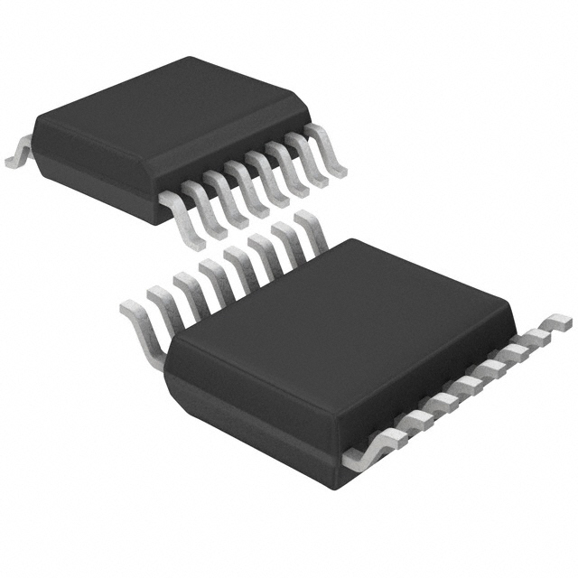
ICS91309 comes in a 16-pin 150 mil SOIC, SSOP or
4.40mm TSSOP package. In the absence of REF input,
the device will enter a powerdown mode. In this mode, the
PLL is turned off and the output buffers are pulled low.
Power down mode provides the lowest power consumption
for a standby condition.
REF
1
16
CLKOUT
CLKA1
2
15
CLKA4
CLKA2
3
14
CLKA3
VDD
4
13
VDD
GND
5
12
GND
CLKB1
6
11
CLKB4
CLKB2
7
10
CLKB3
FS2
8
9
ICS91309
The ICS91309 provides synchronization between the
input and output. The synchronization is established via
CLKOUT feed back to the input of the PLL. Since the skew
between the input and output is less than +/- 350 pS, the
part acts as a zero delay buffer.
Zero input - output delay
Frequency range 10 - 133 MHz (3.3V)
5V tolerant input REF
High loop filter bandwidth ideal for Spread Spectrum
applications.
Less than 125 ps cycle to cycle Jitter
Skew controlled outputs
Available in 16 pin, 150 mil SSOP, SOIC & 4.40mm
TSSOP packages
Skew: Group-to-Group:
很抱歉,暂时无法提供与“91309AGILFT”相匹配的价格&库存,您可以联系我们找货
免费人工找货