ICS9212-13
Direct Rambus™ Clock Generator
General Description
Features
The ICS9212-13 is a High-speed clock generator providing
up to 600 MHz differential clock source for direct Rambus™
memory system. It includes DDLL (Distributed Delay
locked loop) and phase detection mechanism to
synchronize the direct Rambus™ channel clock to an
external system clock. ICS9212-13 provides a solution for
a broad range of Direct Rambus memory applications. The
device works in conjunction with the ICS9250-09.
•
•
The ICS9212-13 power management support system
turns “off” the Rambus™ channel clock to minimize power
consumption for mobile and other power–sensitive
applications. In “clock off” mode the device remains “on”
while the output is disabled, allowing fast transitions
between clock-off and clock–on states. In “power down”
mode it completely powers down for minimum power
dissipation.
•
•
•
•
•
Compatible with all Direct Rambus™ based IC s
Up to 600 MHz differential clock source for direct
Rambus™ memory system
Cycle to cycle jitter is less than 40ps
3.3 + 5% supply
Synchronization flexibility: Supports Systems that
need clock domains of Rambus channel to
synchronize with system or processor clock, or
systems that do not require synchronization of the
Rambus clock to another system clock
Excellent power management support
REFCLK input is from the ICS9250-09.
The ICS9212-13 meets the requirements for input frequency
tracking when the input frequency clock is using Spread
Spectrum clocking and also the optimum bandwidth is
maintained while attenuating the jitter of the reference
signal.
Block Diagram
BUSCLK_STOP#
PD#
FS(0:1)
Test MUX
Bypass MUX
GND
Bypclk
PLLclk
Refclk
B
PLL
A
Multi(0:1)
Pclk/M
Synclk/N
0272F—08/08/07
PAclk
Phase
Detector
2
BUSCLKT
BUSCLKC
Phase
Aligner
GND
VDDREF
REFCLK
VDD1
GND1
GND3
PCLK/M
SYNCLK/N
GND2
VDD2
VDDPD
BUSCLK_STOP#
PD#
1
2
3
4
5
6
7
8
9
10
11
12
ICS9212-13
Pin Configuration
24
23
22
21
20
19
18
17
16
15
14
13
FS0
FS1
VDD-OUT
GND-OUT
BUSCLKT
N/C
BUSCLKC
GND-OUT
VDD-OUT
MULTI0
MULTI1
FS2
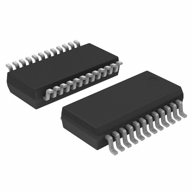
24-Pin 150 Mil SSOP
�ICS9212-13
Pin Descriptions
Pin #
Name
Type
Description
1
VDDREF
REFV
Reference voltage for refclk, to be connected to CK133
2
3
4
5
REFCLK
VDD1
GND1
GND3
IN
PWR
PWR
PWR
6,7
PCLK/M, SYNCLK/N
IN
8
9
GND2
VDD2
PWR
PWR
10
VDDPD
REFV
11
BUSCLK_ STOP#
IN
12
PD#
IN
14,15
MULTI (0:1)
IN
16
17
VDD_OUT
GND_OUT
PWR
PWR
18
BUSCLKC
OUT
19
N/C
N/C
20
BUSCLKT
OUT
21
22
GND_OUT
VDD_OUT
PWR
PWR
13,23,24
FS(0:2)
IN
Reference clock, to be connected to CK133
3.3 V power supply used for PLL
Ground for PLL
Ground for control inputs
Phase controller input, used to drive a phase aligner
that adjusts the phase of the busclk.
Ground for phase aligner
3.3 V power supply used for phase aligner
Reference voltage for phase detector inputs connected
to the controller
Active low output enable/disable
3.3V CMOS active low power down, the device is
powered down when the "(PD#) =0"
3.3V CMOS PLL Multiplier select, logic for selecting
the multiply ratio for the PLL from the input REFCLK
3.3V supply for clock out puts
Ground for clock outputs
Out put clock connected to the Rambus channel. This
output is the complement of BUSCLK
NOT USED
Output clock connected to the Rambus channel. This
output is the true component of BUSCLK
Ground for clock outputs
3.3V supply for clock out puts
3.3V CMOS Mode control, used in selecting bypass,
test, normal, and output test (OE)
0272F—08/08/07
2
�ICS9212-13
PLL Divider Selection and PLL Values (PLLCLK = REFCLK*A/B)
Multo
0
0
1
1
Mult1
0
1
0
1
A
4
6
16
8
B
1
1
3
1
PLLCLK for REFCLK=50MHz
Reserved
300
266.7
400
PLLCLK for REFCLK=66.66MHz
266.6
400.0
355.5
533.3
Bypass and Test Mode Selection
Mode
FS0
FS1
FS2
Bypclk (int.)
BusClk
BusClkB
Normal
0
0
0
Gnd
PAclk
PAclkB
Bypass
1
0
0
PLLclk
PLLclk
PLLclkB
Test
1
1
0
Refclk
Refclk
RefclkB
Vendor Test A
0
0
1
-
-
-
Vendor Test B
1
0
1
-
-
-
Reserved
1
1
1
-
-
-
Output Test (OE)
0
1
X
-
Hi-Z
Hi-Z
Power Management Modes
State
NORMAL
Clk Off
Powerdown
PwrDnB
1
1
0
StopB
1
0
X
0272F—08/08/07
3
�ICS9212-13
Absolute Maximum Ratings
Supply Voltage . . . . . . . . . . . . . . . . . . . . . . . . . 4.0 V
Logic Inputs . . . . . . . . . . . . . . . . . . . . . . . . . . . GND –0.5 V to VDD +0.5 V
Ambient Operating Temperature . . . . . . . . . . 0°C to +70°C
Storage Temperature . . . . . . . . . . . . . . . . . . . . –65°C to +150°C
Stresses above those listed under Absolute Maximum Ratings may cause permanent damage to the device. These
ratings are stress specifications only and functional operation of the device at these or any other conditions above those
listed in the operational sections of the specifications is not implied. Exposure to absolute maximum rating conditions
for extended periods may affect product reliability.
Electrical Characteristics-input/supply/Outputs
Parameters
Supply Voltage
Refclk Input cycle time
Input cycle-to-cycle Jitter
Input Duty cycle over 10k cycles
Input frequency of modulation
Modulation index
Phase detector input cycle time at PDclk/M & Synclk/N
Initial phase error at phase detector inputs
Phase detector input duty cycle over 10k cycles
Input rise & fall times ( measured at 20%-80% of input voltage) for
PDCLK/M & SYNCLK/N,&REfCLK
Input capacitance at PDCLK/M,Synclk/N,&REFCLK
Input Capacitance matching at PCLK/M & SYNCLK/N
Input capacitance at CMOS pins
Input (CMOS) signal low voltage
Input (CMOS) signal high voltage
Symbol
VDD
t CYCLE,IN
t J,IN
t CYCLE,PD
Terr,init
DCIN,PD
Min
3.135
10
40%
30
0.25
30
-0.5
25%
Max
3.465
40
250
60%
33
0.5
100
0.5
75%
t CYCLE,PD
t CYCLE,PD
TIR,TIF
-
1
ns
CIN,PD
DCIN,PD
CIN,CMOS
VIL
VIH
0.7
7
0.5
10
0.3
-
pF
pF
pF
Vdd
Vdd
DCIN
Fm,in
PM,IN
Unit
V
ns
ps
tCYCLE
kHz
%
ns
VIL,R
-
0.3
Vddi,R
0.7
-
0.3
Vddi,R
Vddi,PD
Input signal high voltage for PD inputs and STOP
VIH,R
VIL,PD
V IH,PD
0.7
-
Vddi,PD
Input supply referance for REFCLK
V DD,IR
1.3
3.465
V
Input supply referance vfor PD inputs
VDDI,PD
1.3
3.465
V
Phase detector phase error for distributed loop measured at
PDCLK/M & SYNCLK/N(rising
t ERR,PD
-100
100
ps
Cycle cycle time
t CYCLE
2.5
3.75
ns
tJ
-
40
ps
REFCLK input low voltage
REFCLK input high voltage
Input signal low voltage for PD inputs and STOP
Cycle-to-cycle jitter at Busclk/BUSCLKB (533 MHz)
Total jitter over 1 - 6 cycles (533MHz)
Phase aligner, phase step size (BSCLK/BUSCLKB)
PLL out put phase error when tracking SSC
Out put crossing-point voltage
Output voltage swing
Output high voltage
Out put duty cycle over 10k cycle
Output cycle -to-cycle duty cycle error
Output rise & fall times ( measured at 20%-80% of output voltage)
Difference between rise and fall times on a single device(20%-80%)
Opearting Supply Current
tJ
-
30
ps
t STEP
1
-
ps
t ERR,SSC
-100
100
ps
VX
1.3
1.8
V
VCOS
0.4
0.6
V
VH
DC
2
60%
50
500
V
t DC,ERR
t CR,t CF
40%
300
t CR,CF
-
100
ps
150
mA
IDD
0272F—08/08/07
4
tCYCLE
ps
ps
�ICS9212-13
Recommended Layout
General Layout Precautions:
1) Use a ground plane on the top layer of
the PCB in all areas not used by traces.
2) Make all power traces and vias as wide
as possible to lower inductance.
Capacitor Values:
C3 : 100pF ceramic
All unmarked capacitors are 0.01µF ceramic
Connections to VDD:
0272F—08/08/07
5
�ICS9212-13
SYMBOL
A
A1
A2
B
C
D
E
e
H
L
N
S
∝
X
COMMON
DIMENSIONS
MIN. NOM. MAX.
.061
.064
.068
.004
.006
.0098
.055
.058
.061
.008
.010
.012
.0075
.008
.0098
SEE VARIATIONS
.150
.155
.157
.025 BSC
.230
.236
.244
.010
.013
.016
SEE VARIATIONS
SEE VARIATIONS
0°
5°
8°
0.85
0.93
.100
VARIATIONS
AA
AB
AC
AD
D
MIN.
.189
.337
.337
.386
NOM.
.194
.342
.342
.391
S
MAX.
.196
.344
.344
.393
MIN.
.0020
.0500
.0250
.0250
NOM.
.0045
.0525
.0275
.0280
MAX.
.0076
.0550
.0300
.0300
N
16
20
24
28
150 mil SSOP Package
Diminisions are in inches
Ordering Information
ICS9212yF-13LF
Example:
ICS XXXX y F - PPLF T
Designation for tape and reel packaging
Lead Free, RoHS Compliant (Optional)
Pattern Number (2 or 3 digit number for parts with ROM code patterns)
Package Type
F = SSOP
Revision Designator (will not correlate with datasheet revision)
Device Type (consists of 3 or 4 digit numbers)
0272F—08/08/07
Prefix
ICS = Standard Device
6
�ICS9212-13
Revision History
Rev.
F
Issue Date Description
08/08/07 Fixed typo on Electrical Characteristics.
0272F—08/08/07
7
Page #
4
�IMPORTANT NOTICE AND DISCLAIMER
RENESAS ELECTRONICS CORPORATION AND ITS SUBSIDIARIES (“RENESAS”) PROVIDES TECHNICAL
SPECIFICATIONS AND RELIABILITY DATA (INCLUDING DATASHEETS), DESIGN RESOURCES (INCLUDING
REFERENCE DESIGNS), APPLICATION OR OTHER DESIGN ADVICE, WEB TOOLS, SAFETY INFORMATION, AND
OTHER RESOURCES “AS IS” AND WITH ALL FAULTS, AND DISCLAIMS ALL WARRANTIES, EXPRESS OR IMPLIED,
INCLUDING, WITHOUT LIMITATION, ANY IMPLIED WARRANTIES OF MERCHANTABILITY, FITNESS FOR A
PARTICULAR PURPOSE, OR NON-INFRINGEMENT OF THIRD PARTY INTELLECTUAL PROPERTY RIGHTS.
These resources are intended for developers skilled in the art designing with Renesas products. You are solely responsible
for (1) selecting the appropriate products for your application, (2) designing, validating, and testing your application, and (3)
ensuring your application meets applicable standards, and any other safety, security, or other requirements. These
resources are subject to change without notice. Renesas grants you permission to use these resources only for
development of an application that uses Renesas products. Other reproduction or use of these resources is strictly
prohibited. No license is granted to any other Renesas intellectual property or to any third party intellectual property.
Renesas disclaims responsibility for, and you will fully indemnify Renesas and its representatives against, any claims,
damages, costs, losses, or liabilities arising out of your use of these resources. Renesas' products are provided only subject
to Renesas' Terms and Conditions of Sale or other applicable terms agreed to in writing. No use of any Renesas resources
expands or otherwise alters any applicable warranties or warranty disclaimers for these products.
(Rev.1.0 Mar 2020)
Corporate Headquarters
Contact Information
TOYOSU FORESIA, 3-2-24 Toyosu,
Koto-ku, Tokyo 135-0061, Japan
www.renesas.com
For further information on a product, technology, the most
up-to-date version of a document, or your nearest sales
office, please visit:
www.renesas.com/contact/
Trademarks
Renesas and the Renesas logo are trademarks of Renesas
Electronics Corporation. All trademarks and registered
trademarks are the property of their respective owners.
© 2020 Renesas Electronics Corporation. All rights reserved.
�