ICS953002
Integrated
Circuit
Systems, Inc.
Programmable Timing Control Hub™ for Next Gen P4™ processor
Recommended Application:
Chipset for P4 type processor with PCI-Express
Output Features:
•
2 - 0.7V current-mode differential CPU pairs
•
1 - 0.7V current-mode differential CPU/PCI-Express
selectable pair
•
6 - PCI, 33MHz
•
2 - REF, 14.318MHz
•
3 - 3V66, 66.66MHz
•
1 - 48MHz
•
1 - 24/48MHz
•
5 - PCI-Express 0.7V current mode differential pairs
Features/Benefits:
•
Programmable output frequency.
•
Programmable asynchronous 3V66&PCI frequency.
•
Programmable asynchronous PCI-Express frequency.
•
Programmable output divider ratios.
•
Programmable output skew.
•
Programmable spread percentage for EMI control.
•
Watchdog timer technology to reset system if system
malfunctions.
•
Programmable watch dog safe frequency.
•
Support I2C Index read/write and block read/write
operations.
•
Uses external 14.318MHz reference input, external
crystal load caps are required for frequency tuning.
Key Specifications:
•
CPU outputs cycle-cycle jitter < 85ps
•
3V66 outputs cycle-cycle jitter < 250ps
•
PCI outputs cycle-cycle jitter < 500ps
B0b4
FS4
0
0
0
0
0
0
0
0
0
0
0
0
0
0
0
0
1
1
1
1
1
1
1
1
1
1
1
1
1
1
1
1
B0b3
FS3
0
0
0
0
0
0
0
0
1
1
1
1
1
1
1
1
0
0
0
0
0
0
0
0
1
1
1
1
1
1
1
1
Pin Configuration
B0b2
FSL2
0
0
0
0
1
1
1
1
0
0
0
0
1
1
1
1
0
0
0
0
1
1
1
1
0
0
0
0
1
1
1
1
B0b1
FSL1
0
0
1
1
0
0
1
1
0
0
1
1
0
0
1
1
0
0
1
1
0
0
1
1
0
0
1
1
0
0
1
1
B0b0
FSL0
0
1
0
1
0
1
0
1
0
1
0
1
0
1
0
1
0
1
0
1
0
1
0
1
0
1
0
1
0
1
0
1
PCI-EX
MHz
100.00
100.00
100.00
100.00
N/A
100.00
100.00
100.00
100.00
100.00
100.00
100.00
100.00
100.00
100.00
100.00
100.00
100.00
100.00
100.00
N/A
100.00
100.00
100.00
100.00
100.00
100.00
100.00
N/A
100.00
100.00
100.00
AGP
MHz
66.66
66.66
66.66
66.66
N/A
66.66
66.66
66.66
66.66
66.66
66.66
66.66
66.66
66.66
66.66
66.66
66.66
66.66
66.66
66.66
N/A
66.66
66.66
66.66
66.66
66.66
66.66
66.66
N/A
66.66
66.66
66.66
PCI
MHz
33.33
33.33
33.33
33.33
N/A
33.33
33.33
33.33
33.33
33.33
33.33
33.33
33.33
33.33
33.33
33.33
33.33
33.33
33.33
33.33
N/A
33.33
33.33
33.33
33.33
33.33
33.33
33.33
N/A
33.33
33.33
33.33
CPU
MHz
266.66
133.33
200.00
166.66
N/A
100.00
400.00
200.00
100.00
133.33
200.00
166.66
100.00
133.33
200.00
166.66
266.66
133.33
200.00
166.66
N/A
100.00
400.00
200.00
266.66
133.33
200.00
166.66
N/A
100.00
400.00
200.00
VDDA
GND
VDDREF
**FSL0/REF0
FSL1/REF1
1
2
3
4
5
56
55
54
53
52
GND
IREF
CPUCLKT0
CPUCLKC0
GNDCPU
X1 6
X2 7
GNDREF 8
VttPWR_GD/PD# 9
VDDPCI 10
**FSL2/PCICLK0 11
51
50
49
48
47
46
CPUCLKT1
CPUCLKC1
VDDCPU
SDATA
CPUCLKT2_ITP/PCIEXT0
CPUCLKC2_ITP/PCIEXC0
45
44
43
42
41
40
39
38
37
36
35
34
33
32
31
30
29
VDDPCIEX
PCIEXT1
PCIEXC1
PCIEXT2
PCIEXC2
GNDPCIEX
VDDPCIEX
PCIEXT3
PCIEXC3
PCIEXT4
PCIEXC4
PCIEXT5/CPU_STOP#*
PCIEXC5/PCI_PCIEX_STOP#*
GNDPCIEX
SCLK
GND3V66
3V66_0
**FS3/~PCICLK1
PCICLK2
PCICLK3
GNDPCI
VDDPCI
PCICLK4
PCICLK5
GNDPCI
*Turbo#
Reset#
VDD48
**Mode0/48MHz
*Sel24_48#/24_48MHz
GND48
VDD3V66
**ITP_EN/3V66_2
**FS4/3V66_1
12
13
14
15
16
17
18
19
20
21
22
23
24
25
26
27
28
ICS953002
Functionality
56-Pin SSOP
*These inputs have 120K internal pull-up resistors to VDD.
**These inputs have 120K internal pull-down resistors to GND.
~This output is default 2X drive strength.
0924—11/18/09
�Integrated
Circuit
Systems, Inc.
ICS953002
Pin Description
PIN #
PIN NAME
TYPE
1
2
3
VDDA
GND
VDDREF
4
**FSL0/REF0
I/O
5
FSL1/REF1
I/O
6
7
8
X1
X2
GNDREF
9
VttPWR_GD/PD#
10
VDDPCI
PWR
PWR
PWR
IN
OUT
PWR
IN
PWR
DESCRIPTION
3.3V power for the PLL core.
Ground pin.
Ref, XTAL power supply, nominal 3.3V
3.3V tolerant input for CPU frequency selection. Refer to input electrical
characteristics for Vil_FS and Vih_FS values. / 14.318 MHz reference
3.3V tolerant input for CPU frequency selection. Refer to input electrical
characteristics for Vil_FS and Vih_FS values. / 14.318 MHz reference
Crystal input, Nominally 14.318MHz.
Crystal output, Nominally 14.318MHz
Ground pin for the REF outputs.
This 3.3V LVTTL input is a level sensitive strobe used to determine when
latch inputs are valid and are ready to be sampled. This is an active high
input. / Asynchronous active low input pin used to power down the device
into a low power state.
Power supply for PCI clocks, nominal 3.3V
3.3V tolerant input for CPU frequency selection. Refer to input electrical
characteristics for Vil_FS and Vih_FS values. / 3.3V PCI clock output.
11
**FSL2/PCICLK0
I/O
12
13
14
15
16
17
18
19
**FS3/~PCICLK1
PCICLK2
PCICLK3
GNDPCI
VDDPCI
PCICLK4
PCICLK5
GNDPCI
I/O
OUT
OUT
PWR
PWR
OUT
OUT
PWR
20
*Turbo#
IN
Real time input pin to change frequency to a pre-programmed under or over
clock entries located in the Rom table.
21
Reset#
OUT
Real time system reset signal for frequency gear ratio change or watchdog
timer timeout. This signal is active low.
22
VDD48
PWR
23
**Mode0/48MHz
I/O
24
*Sel24_48#/24_48MHz
I/O
25
26
GND48
VDD3V66
PWR
PWR
Frequency select latch input pin / 3.3V PCI clock output.
PCI clock output.
PCI clock output.
Ground pin for the PCI outputs
Power supply for PCI clocks, nominal 3.3V
PCI clock output.
PCI clock output.
Ground pin for the PCI outputs
Power pin for the 48MHz output.3.3V
Function select pin, 1=Mobile Mode, 0=Desktop Mode / 48MHz clock output.
3.3V.
Latched select input for 24/48MHz output / 24/48MHz clock output.
1=24MHz, 0 = 48MHz.
Ground pin for the 48MHz outputs
Power pin for the 3.3V 66MHz clocks.
27
**ITP_EN/3V66_2
I/O
3.3V 66.66MHz clock output./
ITP_EN: latched input to select pin functionality
1 = CPU_2_ITP pair
0 = PCI-EX0 pair
28
**FS4/3V66_1
I/O
Frequency select latch input pin / 66.66MHz clock output. 3.3V
0924—11/18/09
2
�Integrated
Circuit
Systems, Inc.
ICS953002
Pin Description (Continued)
PIN #
PIN NAME
TYPE
29
30
31
32
3V66_0
GND3V66
SCLK
GNDPCIEX
PCIEXC5/PCI_PCIEX_STO
P#*
OUT
PWR
IN
PWR
33
OUT
DESCRIPTION
3.3V 66.66MHz clock output
Ground pin for the 3.3V 66MHz clocks
Clock pin of SMBus circuitry, 5V tolerant.
Ground pin for the PCI-EX outputs
Complement clock of differential PCI_Express pair. / Active low signal that
stops all PCI and PCIEX clocks besides the free running clocks
34
PCIEXT5/CPU_STOP#*
OUT
True clock of differential PCI_Express pair./Stops all CPUCLK besides the
free running clocks
35
36
37
38
39
40
41
42
43
44
45
PCIEXC4
PCIEXT4
PCIEXC3
PCIEXT3
VDDPCIEX
GNDPCIEX
PCIEXC2
PCIEXT2
PCIEXC1
PCIEXT1
VDDPCIEX
OUT
OUT
OUT
OUT
PWR
PWR
OUT
OUT
OUT
OUT
PWR
Complement clock of differential PCI_Express pair.
True clock of differential PCI_Express pair.
Complement clock of differential PCI_Express pair.
True clock of differential PCI_Express pair.
Power supply for PCI Express clocks, nominal 3.3V
Ground pin for the PCI-EX outputs
Complement clock of differential PCI_Express pair.
True clock of differential PCI_Express pair.
Complement clock of differential PCI_Express pair.
True clock of differential PCI_Express pair.
Power supply for PCI Express clocks, nominal 3.3V
46
CPUCLKC2_ITP/PCIEXC0
OUT
Complementary clock of differential pair CPU outputs. These are current
mode outputs. External resistors are required for voltage bias./
Complement clock of differential PCIEX pair
47
CPUCLKT2_ITP/PCIEXT0
OUT
48
49
SDATA
VDDCPU
I/O
PWR
50
CPUCLKC1
OUT
Complementary clock of differential pair CPU outputs. These are current
mode outputs. External resistors are required for voltage bias.
51
CPUCLKT1
OUT
True clock of differential pair CPU outputs. These are current mode
outputs. External resistors are required for voltage bias.
52
GNDCPU
PWR
53
CPUCLKC0
OUT
54
CPUCLKT0
OUT
True clock of differential pair CPU outputs. These are current mode
outputs. External resistors are required for voltage bias.
55
IREF
OUT
This pin establishes the reference current for the differential current-mode
output pairs. This pin requires a fixed precision resistor tied to ground in
order to establish the appropriate current. 475 ohms is the standard value.
56
GND
PWR
Ground pin.
True clock of differential pair CPU outputs. These are current mode
outputs. External resistors are required for voltage bias. / True clock of
differential PCIEX pair
Data pin for SMBus circuitry, 5V tolerant.
Supply for CPU clocks, 3.3V nominal
Ground pin for the CPU outputs
Complementary clock of differential pair CPU outputs. These are current
mode outputs. External resistors are required for voltage bias.
0924—11/18/09
3
�Integrated
Circuit
Systems, Inc.
ICS953002
General Description
ICS953002 is a 56-pin clock chip for P4 type processors with PCI-Express.
The ICS953002 is part of a whole new line of ICS clock generators and buffers called TCH™ (Timing Control Hub). This part
incorporates ICS's newest clock technology which offers more robust features and functionality. Employing the use of a
serially programmable I2C interface, this device can adjust the output clocks by configuring the frequency setting, the output
divider ratios, selecting the ideal spread percentage, the output skew, the output strength, and enabling/disabling each
individual output clock. M/N control can configure output frequency with resolution up to 0.1MHz increment.
Block Diagram
PLL2
Frequency
Dividers
48MHz
24_48MHz
X1
X2
XTAL
REF (1:0)
CPUCLKT (1:0)
CPUCLKC (1:0)
FS (4:0)
CPUCLKT2_ITP/PCIEXT0
SCLK
Sel24_48#
SDATA
MODE0
Control
Logic
Programmable
Spread
PLL1
Programmable
Frequency
Dividers
STOP
Logic
CPUCLKC2_ITP/PCIEXC0
3V66 (2:0)
PCICLK (5:0)
VTTPWRGD#
PCI-EXT (5:1)
PD#
PCI-EXC (5:1)
Turbo#
RESET#
I REF
0924—11/18/09
4
�Integrated
Circuit
Systems, Inc.
ICS953002
Table 1a. CPU PLL1 Turbo Rom
FS4
B0b4
0
0
0
0
0
0
0
0
0
0
0
0
0
0
0
0
FS3
B0b3
0
0
0
0
0
0
0
0
0
0
0
0
0
0
0
0
FSL2
B0b2
0
0
0
0
0
0
0
0
0
0
0
0
0
0
0
0
FSL1
B0b1
0
0
0
0
0
0
0
0
0
0
0
0
0
0
0
0
FSL0
B0b0
0
0
0
0
0
0
0
0
0
0
0
0
0
0
0
0
0
0
0
0
0
0
0
0
0
0
0
0
0
0
0
0
0
0
0
0
0
0
0
0
0
0
0
0
0
0
0
0
0
0
0
0
0
0
0
0
0
0
0
0
0
0
0
0
0
0
0
0
0
0
0
0
0
0
0
0
0
0
0
0
0
0
0
0
0
0
0
0
0
0
0
0
0
0
0
0
CPUFS4 CPUFS3 CPUFS2 CPUFS1 CPUFS0
B1bit4 B1bit3 B1bit2 B1bit1 B1bit0
0
0
0
0
0
0
0
0
0
1
0
0
0
1
0
0
0
0
1
1
0
0
1
0
0
0
0
1
0
1
0
0
1
1
0
0
0
1
1
1
0
1
0
0
0
0
1
0
0
1
0
1
0
1
0
0
1
0
1
1
0
1
1
0
0
0
1
1
0
1
0
1
1
1
0
0
1
1
1
1
1
0
0
0
0
1
0
0
0
1
1
0
0
1
0
1
0
0
1
1
1
0
1
0
0
1
0
1
0
1
1
0
1
1
0
1
0
1
1
1
1
1
0
0
0
1
1
0
0
1
1
1
0
1
0
1
1
0
1
1
1
1
1
0
0
1
1
1
0
1
1
1
1
1
0
1
1
1
1
1
0924—11/18/09
5
CPU
Mhz
N/A
N/A
N/A
N/A
N/A
N/A
N/A
N/A
266.67
269.33
274.67
280.00
285.33
290.67
293.33
296.00
222.22
224.44
228.89
233.33
237.78
242.22
244.44
246.66
266.67
269.33
274.67
280.00
285.33
290.67
293.33
296.00
PCI-EX
(default)
N/A
N/A
N/A
N/A
N/A
N/A
N/A
N/A
100.00
101.00
103.00
105.00
107.00
109.00
110.00
111.00
111.11
112.22
114.44
116.67
118.89
121.11
122.22
123.33
100.00
101.00
103.00
105.00
107.00
109.00
110.00
111.00
AGP
PCI
(default) (default)
N/A
N/A
N/A
N/A
N/A
N/A
N/A
N/A
N/A
N/A
N/A
N/A
N/A
N/A
N/A
N/A
66.67
33.33
67.33
33.67
68.67
34.33
70.00
35.00
71.33
35.67
72.67
36.33
73.33
36.67
74.00
37.00
66.67
33.33
67.33
33.67
68.67
34.33
70.00
35.00
71.33
35.67
72.67
36.33
73.33
36.67
74.00
37.00
66.67
33.33
67.33
33.67
68.67
34.33
70.00
35.00
71.33
35.67
72.67
36.33
73.33
36.67
74.00
37.00
Spreading
%
Down Sp 0-0.5 %
Center +/- 0.25
Center +/- 0.25
Center +/- 0.25
Center +/- 0.25
Center +/- 0.25
Center +/- 0.25
Center +/- 0.25
Down Sp 0-0.5 %
Center +/- 0.25
Center +/- 0.25
Center +/- 0.25
Center +/- 0.25
Center +/- 0.25
Center +/- 0.25
Center +/- 0.25
Down Sp 0-0.5 %
Center +/- 0.25
Center +/- 0.25
Center +/- 0.25
Center +/- 0.25
Center +/- 0.25
Center +/- 0.25
Center +/- 0.25
Down Sp 0-0.5 %
Center +/- 0.25
Center +/- 0.25
Center +/- 0.25
Center +/- 0.25
Center +/- 0.25
Center +/- 0.25
Center +/- 0.25
�Integrated
Circuit
Systems, Inc.
ICS953002
Table 1a. CPU PLL1 Turbo Rom (continued)
FS4
B0b4
0
0
0
0
0
0
0
0
0
0
0
0
0
0
0
0
0
0
0
0
0
0
0
0
0
0
0
0
0
0
0
0
FS3
B0b3
0
0
0
0
0
0
0
0
0
0
0
0
0
0
0
0
0
0
0
0
0
0
0
0
0
0
0
0
0
0
0
0
FSL2
B0b2
0
0
0
0
0
0
0
0
0
0
0
0
0
0
0
0
0
0
0
0
0
0
0
0
0
0
0
0
0
0
0
0
FSL1
B0b1
0
0
0
0
0
0
0
0
0
0
0
0
0
0
0
0
0
0
0
0
0
0
0
0
0
0
0
0
0
0
0
0
FSL0
B0b0
1
1
1
1
1
1
1
1
1
1
1
1
1
1
1
1
1
1
1
1
1
1
1
1
1
1
1
1
1
1
1
1
CPUFS4 CPUFS3 CPUFS2 CPUFS1 CPUFS0
B1bit4 B1bit3 B1bit2 B1bit1 B1bit0
0
0
0
0
0
0
0
0
0
1
0
0
0
1
0
0
0
0
1
1
0
0
1
0
0
0
0
1
0
1
0
0
1
1
0
0
0
1
1
1
0
1
0
0
0
0
1
0
0
1
0
1
0
1
0
0
1
0
1
1
0
1
1
0
0
0
1
1
0
1
0
1
1
1
0
0
1
1
1
1
1
0
0
0
0
1
0
0
0
1
1
0
0
1
0
1
0
0
1
1
1
0
1
0
0
1
0
1
0
1
1
0
1
1
0
1
0
1
1
1
1
1
0
0
0
1
1
0
0
1
1
1
0
1
0
1
1
0
1
1
1
1
1
0
0
1
1
1
0
1
1
1
1
1
0
1
1
1
1
1
0924—11/18/09
6
CPU
Mhz
N/A
N/A
N/A
N/A
N/A
N/A
N/A
N/A
133.33
134.67
137.33
140.00
142.67
145.33
146.67
148.00
111.11
112.22
114.44
116.67
118.89
121.11
122.22
123.33
133.33
134.67
137.33
140.00
142.67
145.33
146.67
148.00
PCI-EX
(default)
N/A
N/A
N/A
N/A
N/A
N/A
N/A
N/A
100.00
101.00
103.00
105.00
107.00
109.00
110.00
111.00
111.11
112.22
114.44
116.67
118.89
121.11
122.22
123.33
100.00
101.00
103.00
105.00
107.00
109.00
110.00
111.00
AGP
PCI
(default) (default)
N/A
N/A
N/A
N/A
N/A
N/A
N/A
N/A
N/A
N/A
N/A
N/A
N/A
N/A
N/A
N/A
66.67
33.33
67.33
33.67
68.67
34.33
70.00
35.00
71.33
35.67
72.67
36.33
73.33
36.67
74.00
37.00
66.67
33.33
67.33
33.67
68.67
34.33
70.00
35.00
71.33
35.67
72.67
36.33
73.33
36.67
74.00
37.00
66.67
33.33
67.33
33.67
68.67
34.33
70.00
35.00
71.33
35.67
72.67
36.33
73.33
36.67
74.00
37.00
Spreading
%
Down Sp 0-0.5 %
Center +/- 0.25
Center +/- 0.25
Center +/- 0.25
Center +/- 0.25
Center +/- 0.25
Center +/- 0.25
Center +/- 0.25
Down Sp 0-0.5 %
Center +/- 0.25
Center +/- 0.25
Center +/- 0.25
Center +/- 0.25
Center +/- 0.25
Center +/- 0.25
Center +/- 0.25
Down Sp 0-0.5 %
Center +/- 0.25
Center +/- 0.25
Center +/- 0.25
Center +/- 0.25
Center +/- 0.25
Center +/- 0.25
Center +/- 0.25
Down Sp 0-0.5 %
Center +/- 0.25
Center +/- 0.25
Center +/- 0.25
Center +/- 0.25
Center +/- 0.25
Center +/- 0.25
Center +/- 0.25
�Integrated
Circuit
Systems, Inc.
ICS953002
Table 1a. CPU PLL1 Turbo Rom (continued)
FS4
B0b4
0
0
0
0
0
0
0
0
0
0
0
0
0
0
0
0
0
0
0
0
0
0
0
0
0
0
0
0
0
0
0
0
FS3
B0b3
0
0
0
0
0
0
0
0
0
0
0
0
0
0
0
0
0
0
0
0
0
0
0
0
0
0
0
0
0
0
0
0
FSL2
B0b2
0
0
0
0
0
0
0
0
0
0
0
0
0
0
0
0
0
0
0
0
0
0
0
0
0
0
0
0
0
0
0
0
FSL1
B0b1
1
1
1
1
1
1
1
1
1
1
1
1
1
1
1
1
1
1
1
1
1
1
1
1
1
1
1
1
1
1
1
1
FSL0
B0b0
0
0
0
0
0
0
0
0
0
0
0
0
0
0
0
0
0
0
0
0
0
0
0
0
0
0
0
0
0
0
0
0
CPUFS4 CPUFS3 CPUFS2 CPUFS1 CPUFS0
B1bit4 B1bit3 B1bit2 B1bit1 B1bit0
0
0
0
0
0
0
0
0
0
1
0
0
0
1
0
0
0
0
1
1
0
0
1
0
0
0
0
1
0
1
0
0
1
1
0
0
0
1
1
1
0
1
0
0
0
0
1
0
0
1
0
1
0
1
0
0
1
0
1
1
0
1
1
0
0
0
1
1
0
1
0
1
1
1
0
0
1
1
1
1
1
0
0
0
0
1
0
0
0
1
1
0
0
1
0
1
0
0
1
1
1
0
1
0
0
1
0
1
0
1
1
0
1
1
0
1
0
1
1
1
1
1
0
0
0
1
1
0
0
1
1
1
0
1
0
1
1
0
1
1
1
1
1
0
0
1
1
1
0
1
1
1
1
1
0
1
1
1
1
1
0924—11/18/09
7
CPU
Mhz
N/A
N/A
N/A
N/A
N/A
N/A
N/A
N/A
200.00
202.00
206.00
210.00
214.00
218.00
220.00
222.00
166.67
168.33
171.66
175.00
178.33
181.66
183.33
185.00
200.00
202.00
206.00
210.00
214.00
218.00
220.00
222.00
PCI-EX
(default)
N/A
N/A
N/A
N/A
N/A
N/A
N/A
N/A
100.00
101.00
103.00
105.00
107.00
109.00
110.00
111.00
111.11
112.22
114.44
116.67
118.89
121.11
122.22
123.33
100.00
101.00
103.00
105.00
107.00
109.00
110.00
111.00
AGP
PCI
(default) (default)
N/A
N/A
N/A
N/A
N/A
N/A
N/A
N/A
N/A
N/A
N/A
N/A
N/A
N/A
N/A
N/A
66.67
33.33
67.33
33.67
68.67
34.33
70.00
35.00
71.33
35.67
72.67
36.33
73.33
36.67
74.00
37.00
66.67
33.33
67.33
33.67
68.67
34.33
70.00
35.00
71.33
35.67
72.67
36.33
73.33
36.67
74.00
37.00
66.67
33.33
67.33
33.67
68.67
34.33
70.00
35.00
71.33
35.67
72.67
36.33
73.33
36.67
74.00
37.00
Spreading
%
Down Sp 0-0.5 %
Center +/- 0.25
Center +/- 0.25
Center +/- 0.25
Center +/- 0.25
Center +/- 0.25
Center +/- 0.25
Center +/- 0.25
Down Sp 0-0.5 %
Center +/- 0.25
Center +/- 0.25
Center +/- 0.25
Center +/- 0.25
Center +/- 0.25
Center +/- 0.25
Center +/- 0.25
Down Sp 0-0.5 %
Center +/- 0.25
Center +/- 0.25
Center +/- 0.25
Center +/- 0.25
Center +/- 0.25
Center +/- 0.25
Center +/- 0.25
Down Sp 0-0.5 %
Center +/- 0.25
Center +/- 0.25
Center +/- 0.25
Center +/- 0.25
Center +/- 0.25
Center +/- 0.25
Center +/- 0.25
�Integrated
Circuit
Systems, Inc.
ICS953002
Table 1a. CPU PLL1 Turbo Rom (continued)
FS4
B0b4
0
0
0
0
0
0
0
0
0
0
0
0
0
0
0
0
0
0
0
0
0
0
0
0
0
0
0
0
0
0
0
0
FS3
B0b3
0
0
0
0
0
0
0
0
0
0
0
0
0
0
0
0
0
0
0
0
0
0
0
0
0
0
0
0
0
0
0
0
FSL2
B0b2
0
0
0
0
0
0
0
0
0
0
0
0
0
0
0
0
0
0
0
0
0
0
0
0
0
0
0
0
0
0
0
0
FSL1
B0b1
1
1
1
1
1
1
1
1
1
1
1
1
1
1
1
1
1
1
1
1
1
1
1
1
1
1
1
1
1
1
1
1
FSL0
B0b0
1
1
1
1
1
1
1
1
1
1
1
1
1
1
1
1
1
1
1
1
1
1
1
1
1
1
1
1
1
1
1
1
CPUFS4 CPUFS3 CPUFS2 CPUFS1 CPUFS0
B1bit4 B1bit3 B1bit2 B1bit1 B1bit0
0
0
0
0
0
0
0
0
0
1
0
0
0
1
0
0
0
0
1
1
0
0
1
0
0
0
0
1
0
1
0
0
1
1
0
0
0
1
1
1
0
1
0
0
0
0
1
0
0
1
0
1
0
1
0
0
1
0
1
1
0
1
1
0
0
0
1
1
0
1
0
1
1
1
0
0
1
1
1
1
1
0
0
0
0
1
0
0
0
1
1
0
0
1
0
1
0
0
1
1
1
0
1
0
0
1
0
1
0
1
1
0
1
1
0
1
0
1
1
1
1
1
0
0
0
1
1
0
0
1
1
1
0
1
0
1
1
0
1
1
1
1
1
0
0
1
1
1
0
1
1
1
1
1
0
1
1
1
1
1
0924—11/18/09
8
CPU
Mhz
N/A
N/A
N/A
N/A
N/A
N/A
N/A
N/A
200.00
202.00
206.00
210.00
214.00
218.00
220.00
222.00
166.67
168.33
171.66
175.00
178.33
181.66
183.33
185.00
200.00
202.00
206.00
210.00
214.00
218.00
220.00
222.00
PCI-EX
(default)
N/A
N/A
N/A
N/A
N/A
N/A
N/A
N/A
100.00
101.00
103.00
105.00
107.00
109.00
110.00
111.00
111.11
112.22
114.44
116.67
118.89
121.11
122.22
123.33
100.00
101.00
103.00
105.00
107.00
109.00
110.00
111.00
AGP
PCI
(default) (default)
N/A
N/A
N/A
N/A
N/A
N/A
N/A
N/A
N/A
N/A
N/A
N/A
N/A
N/A
N/A
N/A
66.67
33.33
67.33
33.67
68.67
34.33
70.00
35.00
71.33
35.67
72.67
36.33
73.33
36.67
74.00
37.00
66.67
33.33
67.33
33.67
68.67
34.33
70.00
35.00
71.33
35.67
72.67
36.33
73.33
36.67
74.00
37.00
66.67
33.33
67.33
33.67
68.67
34.33
70.00
35.00
71.33
35.67
72.67
36.33
73.33
36.67
74.00
37.00
Spreading
%
Down Sp 0-0.5 %
Center +/- 0.25
Center +/- 0.25
Center +/- 0.25
Center +/- 0.25
Center +/- 0.25
Center +/- 0.25
Center +/- 0.25
Down Sp 0-0.5 %
Center +/- 0.25
Center +/- 0.25
Center +/- 0.25
Center +/- 0.25
Center +/- 0.25
Center +/- 0.25
Center +/- 0.25
Down Sp 0-0.5 %
Center +/- 0.25
Center +/- 0.25
Center +/- 0.25
Center +/- 0.25
Center +/- 0.25
Center +/- 0.25
Center +/- 0.25
Down Sp 0-0.5 %
Center +/- 0.25
Center +/- 0.25
Center +/- 0.25
Center +/- 0.25
Center +/- 0.25
Center +/- 0.25
Center +/- 0.25
�Integrated
Circuit
Systems, Inc.
ICS953002
Table 1a. CPU PLL1 Turbo Rom (continued)
FS4
FS3
FSL2
FSL1
FSL0
B0b4
0
0
0
0
0
0
0
0
0
0
0
0
0
0
0
0
0
0
0
0
0
0
0
0
0
0
0
0
0
0
0
0
B0b3
0
0
0
0
0
0
0
0
0
0
0
0
0
0
0
0
0
0
0
0
0
0
0
0
0
0
0
0
0
0
0
0
B0b2
1
1
1
1
1
1
1
1
1
1
1
1
1
1
1
1
1
1
1
1
1
1
1
1
1
1
1
1
1
1
1
1
B0b1
0
0
0
0
0
0
0
0
0
0
0
0
0
0
0
0
0
0
0
0
0
0
0
0
0
0
0
0
0
0
0
0
B0b0
0
0
0
0
0
0
0
0
0
0
0
0
0
0
0
0
0
0
0
0
0
0
0
0
0
0
0
0
0
0
0
0
CPUFS4 CPUFS3 CPUFS2 CPUFS1 CPUFS0
B1bit4
0
0
0
0
0
0
0
0
0
0
0
0
0
0
0
0
1
1
1
1
1
1
1
1
1
1
1
1
1
1
1
1
B1bit3
0
0
0
0
0
0
0
0
1
1
1
1
1
1
1
1
0
0
0
0
0
0
0
0
1
1
1
1
1
1
1
1
B1bit2
0
0
0
0
1
1
1
1
0
0
0
0
1
1
1
1
0
0
0
0
1
1
1
1
0
0
0
0
1
1
1
1
B1bit1
0
0
1
1
0
0
1
1
0
0
1
1
0
0
1
1
0
0
1
1
0
0
1
1
0
0
1
1
0
0
1
1
0924—11/18/09
9
B1bit0
0
1
0
1
0
1
0
1
0
1
0
1
0
1
0
1
0
1
0
1
0
1
0
1
0
1
0
1
0
1
0
1
CPU
PCI-EX
Mhz
N/A
N/A
N/A
N/A
N/A
N/A
N/A
N/A
266.67
269.33
274.67
280.00
285.33
290.67
293.33
296.00
222.22
224.44
228.89
233.33
237.78
242.22
244.44
246.66
266.67
269.33
274.67
280.00
285.33
290.67
293.33
296.00
(default)
N/A
N/A
N/A
N/A
N/A
N/A
N/A
N/A
100.00
101.00
103.00
105.00
107.00
109.00
110.00
111.00
111.11
112.22
114.44
116.67
118.89
121.11
122.22
123.33
100.00
101.00
103.00
105.00
107.00
109.00
110.00
111.00
AGP
PCI
(default) (default)
N/A
N/A
N/A
N/A
N/A
N/A
N/A
N/A
N/A
N/A
N/A
N/A
N/A
N/A
N/A
N/A
66.67
33.33
67.33
33.67
68.67
34.33
70.00
35.00
71.33
35.67
72.67
36.33
73.33
36.67
74.00
37.00
66.67
33.33
67.33
33.67
68.67
34.33
70.00
35.00
71.33
35.67
72.67
36.33
73.33
36.67
74.00
37.00
66.67
33.33
67.33
33.67
68.67
34.33
70.00
35.00
71.33
35.67
72.67
36.33
73.33
36.67
74.00
37.00
Spreading
%
Down Sp 0-0.5 %
Center +/- 0.25
Center +/- 0.25
Center +/- 0.25
Center +/- 0.25
Center +/- 0.25
Center +/- 0.25
Center +/- 0.25
Down Sp 0-0.5 %
Center +/- 0.25
Center +/- 0.25
Center +/- 0.25
Center +/- 0.25
Center +/- 0.25
Center +/- 0.25
Center +/- 0.25
Down Sp 0-0.5 %
Center +/- 0.25
Center +/- 0.25
Center +/- 0.25
Center +/- 0.25
Center +/- 0.25
Center +/- 0.25
Center +/- 0.25
Down Sp 0-0.5 %
Center +/- 0.25
Center +/- 0.25
Center +/- 0.25
Center +/- 0.25
Center +/- 0.25
Center +/- 0.25
Center +/- 0.25
�Integrated
Circuit
Systems, Inc.
ICS953002
Table 1a. CPU PLL1 Turbo Rom (continued)
FS4
B0b4
0
0
0
0
0
0
0
0
0
0
0
0
0
0
0
0
0
0
0
0
0
0
0
0
0
0
0
0
0
0
0
0
FS3
B0b3
0
0
0
0
0
0
0
0
0
0
0
0
0
0
0
0
0
0
0
0
0
0
0
0
0
0
0
0
0
0
0
0
FSL2
B0b2
1
1
1
1
1
1
1
1
1
1
1
1
1
1
1
1
1
1
1
1
1
1
1
1
1
1
1
1
1
1
1
1
FSL1
B0b1
0
0
0
0
0
0
0
0
0
0
0
0
0
0
0
0
0
0
0
0
0
0
0
0
0
0
0
0
0
0
0
0
FSL0
B0b0
1
1
1
1
1
1
1
1
1
1
1
1
1
1
1
1
1
1
1
1
1
1
1
1
1
1
1
1
1
1
1
1
CPUFS4 CPUFS3 CPUFS2 CPUFS1 CPUFS0
B1bit4 B1bit3 B1bit2 B1bit1 B1bit0
0
0
0
0
0
0
0
0
0
1
0
0
0
1
0
0
0
0
1
1
0
0
1
0
0
0
0
1
0
1
0
0
1
1
0
0
0
1
1
1
0
1
0
0
0
0
1
0
0
1
0
1
0
1
0
0
1
0
1
1
0
1
1
0
0
0
1
1
0
1
0
1
1
1
0
0
1
1
1
1
1
0
0
0
0
1
0
0
0
1
1
0
0
1
0
1
0
0
1
1
1
0
1
0
0
1
0
1
0
1
1
0
1
1
0
1
0
1
1
1
1
1
0
0
0
1
1
0
0
1
1
1
0
1
0
1
1
0
1
1
1
1
1
0
0
1
1
1
0
1
1
1
1
1
0
1
1
1
1
1
0924—11/18/09
10
CPU
Mhz
N/A
N/A
N/A
N/A
N/A
N/A
N/A
N/A
100.00
101.00
103.00
105.00
107.00
109.00
110.00
111.00
83.33
84.17
85.83
87.50
89.17
90.83
91.67
92.50
100.00
101.00
103.00
105.00
107.00
109.00
110.00
111.00
PCI-EX
(default)
N/A
N/A
N/A
N/A
N/A
N/A
N/A
N/A
100.00
101.00
103.00
105.00
107.00
109.00
110.00
111.00
111.11
112.22
114.44
116.67
118.89
121.11
122.22
123.33
100.00
101.00
103.00
105.00
107.00
109.00
110.00
111.00
AGP
PCI
(default) (default)
N/A
N/A
N/A
N/A
N/A
N/A
N/A
N/A
N/A
N/A
N/A
N/A
N/A
N/A
N/A
N/A
66.67
33.33
67.33
33.67
68.67
34.33
70.00
35.00
71.33
35.67
72.67
36.33
73.33
36.67
74.00
37.00
66.67
33.33
67.33
33.67
68.67
34.33
70.00
35.00
71.33
35.67
72.67
36.33
73.33
36.67
74.00
37.00
66.67
33.33
67.33
33.67
68.67
34.33
70.00
35.00
71.33
35.67
72.67
36.33
73.33
36.67
74.00
37.00
Spreading
%
Down Sp 0-0.5 %
Center +/- 0.25
Center +/- 0.25
Center +/- 0.25
Center +/- 0.25
Center +/- 0.25
Center +/- 0.25
Center +/- 0.25
Down Sp 0-0.5 %
Center +/- 0.25
Center +/- 0.25
Center +/- 0.25
Center +/- 0.25
Center +/- 0.25
Center +/- 0.25
Center +/- 0.25
Down Sp 0-0.5 %
Center +/- 0.25
Center +/- 0.25
Center +/- 0.25
Center +/- 0.25
Center +/- 0.25
Center +/- 0.25
Center +/- 0.25
Down Sp 0-0.5 %
Center +/- 0.25
Center +/- 0.25
Center +/- 0.25
Center +/- 0.25
Center +/- 0.25
Center +/- 0.25
Center +/- 0.25
�Integrated
Circuit
Systems, Inc.
ICS953002
Table 1a. CPU PLL1 Turbo Rom (continued)
FS4
FS3
FSL2
FSL1
FSL0
B0b4
0
0
0
0
0
0
0
0
0
0
0
0
0
0
0
0
0
0
0
0
0
0
0
0
0
0
0
0
0
0
0
0
B0b3
0
0
0
0
0
0
0
0
0
0
0
0
0
0
0
0
0
0
0
0
0
0
0
0
0
0
0
0
0
0
0
0
B0b2
1
1
1
1
1
1
1
1
1
1
1
1
1
1
1
1
1
1
1
1
1
1
1
1
1
1
1
1
1
1
1
1
B0b1
1
1
1
1
1
1
1
1
1
1
1
1
1
1
1
1
1
1
1
1
1
1
1
1
1
1
1
1
1
1
1
1
B0b0
0
0
0
0
0
0
0
0
0
0
0
0
0
0
0
0
0
0
0
0
0
0
0
0
0
0
0
0
0
0
0
0
CPUFS4 CPUFS3 CPUFS2 CPUFS1 CPUFS0
B1bit4
0
0
0
0
0
0
0
0
0
0
0
0
0
0
0
0
1
1
1
1
1
1
1
1
1
1
1
1
1
1
1
1
B1bit3
0
0
0
0
0
0
0
0
1
1
1
1
1
1
1
1
0
0
0
0
0
0
0
0
1
1
1
1
1
1
1
1
B1bit2
0
0
0
0
1
1
1
1
0
0
0
0
1
1
1
1
0
0
0
0
1
1
1
1
0
0
0
0
1
1
1
1
B1bit1
0
0
1
1
0
0
1
1
0
0
1
1
0
0
1
1
0
0
1
1
0
0
1
1
0
0
1
1
0
0
1
1
0924—11/18/09
11
B1bit0
0
1
0
1
0
1
0
1
0
1
0
1
0
1
0
1
0
1
0
1
0
1
0
1
0
1
0
1
0
1
0
1
CPU
PCI-EX
Mhz
N/A
N/A
N/A
N/A
N/A
N/A
N/A
N/A
400.00
404.00
412.00
420.00
428.00
436.00
440.00
444.00
333.33
336.66
343.33
350.00
356.66
363.33
366.66
370.00
400.00
404.00
412.00
420.00
428.00
436.00
440.00
444.00
(default)
N/A
N/A
N/A
N/A
N/A
N/A
N/A
N/A
100.00
101.00
103.00
105.00
107.00
109.00
110.00
111.00
111.11
112.22
114.44
116.67
118.89
121.11
122.22
123.33
100.00
101.00
103.00
105.00
107.00
109.00
110.00
111.00
AGP
PCI
(default) (default)
N/A
N/A
N/A
N/A
N/A
N/A
N/A
N/A
N/A
N/A
N/A
N/A
N/A
N/A
N/A
N/A
66.67
33.33
67.33
33.67
68.67
34.33
70.00
35.00
71.33
35.67
72.67
36.33
73.33
36.67
74.00
37.00
66.67
33.33
67.33
33.67
68.67
34.33
70.00
35.00
71.33
35.67
72.67
36.33
73.33
36.67
74.00
37.00
66.67
33.33
67.33
33.67
68.67
34.33
70.00
35.00
71.33
35.67
72.67
36.33
73.33
36.67
74.00
37.00
Spreading
%
Down Sp 0-0.5 %
Center +/- 0.25
Center +/- 0.25
Center +/- 0.25
Center +/- 0.25
Center +/- 0.25
Center +/- 0.25
Center +/- 0.25
Down Sp 0-0.5 %
Center +/- 0.25
Center +/- 0.25
Center +/- 0.25
Center +/- 0.25
Center +/- 0.25
Center +/- 0.25
Center +/- 0.25
Down Sp 0-0.5 %
Center +/- 0.25
Center +/- 0.25
Center +/- 0.25
Center +/- 0.25
Center +/- 0.25
Center +/- 0.25
Center +/- 0.25
Down Sp 0-0.5 %
Center +/- 0.25
Center +/- 0.25
Center +/- 0.25
Center +/- 0.25
Center +/- 0.25
Center +/- 0.25
Center +/- 0.25
�Integrated
Circuit
Systems, Inc.
ICS953002
Table 1a. CPU PLL1 Turbo Rom (continued)
FS4
FS3
FSL2
FSL1
FSL0
B0b4
0
0
0
0
0
0
0
0
0
0
0
0
0
0
0
0
0
0
0
0
0
0
0
0
0
0
0
0
0
0
0
0
B0b3
0
0
0
0
0
0
0
0
0
0
0
0
0
0
0
0
0
0
0
0
0
0
0
0
0
0
0
0
0
0
0
0
B0b2
1
1
1
1
1
1
1
1
1
1
1
1
1
1
1
1
1
1
1
1
1
1
1
1
1
1
1
1
1
1
1
1
B0b1
1
1
1
1
1
1
1
1
1
1
1
1
1
1
1
1
1
1
1
1
1
1
1
1
1
1
1
1
1
1
1
1
B0b0
1
1
1
1
1
1
1
1
1
1
1
1
1
1
1
1
1
1
1
1
1
1
1
1
1
1
1
1
1
1
1
1
CPUFS4 CPUFS3 CPUFS2 CPUFS1 CPUFS0
B1bit4
0
0
0
0
0
0
0
0
0
0
0
0
0
0
0
0
1
1
1
1
1
1
1
1
1
1
1
1
1
1
1
1
B1bit3
0
0
0
0
0
0
0
0
1
1
1
1
1
1
1
1
0
0
0
0
0
0
0
0
1
1
1
1
1
1
1
1
B1bit2
0
0
0
0
1
1
1
1
0
0
0
0
1
1
1
1
0
0
0
0
1
1
1
1
0
0
0
0
1
1
1
1
B1bit1
0
0
1
1
0
0
1
1
0
0
1
1
0
0
1
1
0
0
1
1
0
0
1
1
0
0
1
1
0
0
1
1
0924—11/18/09
12
B1bit0
0
1
0
1
0
1
0
1
0
1
0
1
0
1
0
1
0
1
0
1
0
1
0
1
0
1
0
1
0
1
0
1
CPU
PCI-EX
Mhz
N/A
N/A
N/A
N/A
N/A
N/A
N/A
N/A
200.00
202.00
206.00
210.00
214.00
218.00
220.00
222.00
166.67
168.33
171.66
175.00
178.33
181.66
183.33
185.00
200.00
202.00
206.00
210.00
214.00
218.00
220.00
222.00
(default)
N/A
N/A
N/A
N/A
N/A
N/A
N/A
N/A
100.00
101.00
103.00
105.00
107.00
109.00
110.00
111.00
111.11
112.22
114.44
116.67
118.89
121.11
122.22
123.33
100.00
101.00
103.00
105.00
107.00
109.00
110.00
111.00
AGP
PCI
(default) (default)
N/A
N/A
N/A
N/A
N/A
N/A
N/A
N/A
N/A
N/A
N/A
N/A
N/A
N/A
N/A
N/A
66.67
33.33
67.33
33.67
68.67
34.33
70.00
35.00
71.33
35.67
72.67
36.33
73.33
36.67
74.00
37.00
66.67
33.33
67.33
33.67
68.67
34.33
70.00
35.00
71.33
35.67
72.67
36.33
73.33
36.67
74.00
37.00
66.67
33.33
67.33
33.67
68.67
34.33
70.00
35.00
71.33
35.67
72.67
36.33
73.33
36.67
74.00
37.00
Spreading
%
Down Sp 0-0.5 %
Center +/- 0.25
Center +/- 0.25
Center +/- 0.25
Center +/- 0.25
Center +/- 0.25
Center +/- 0.25
Center +/- 0.25
Down Sp 0-0.5 %
Center +/- 0.25
Center +/- 0.25
Center +/- 0.25
Center +/- 0.25
Center +/- 0.25
Center +/- 0.25
Center +/- 0.25
Down Sp 0-0.5 %
Center +/- 0.25
Center +/- 0.25
Center +/- 0.25
Center +/- 0.25
Center +/- 0.25
Center +/- 0.25
Center +/- 0.25
Down Sp 0-0.5 %
Center +/- 0.25
Center +/- 0.25
Center +/- 0.25
Center +/- 0.25
Center +/- 0.25
Center +/- 0.25
Center +/- 0.25
�Integrated
Circuit
Systems, Inc.
ICS953002
Table 1a. CPU PLL1 Turbo Rom (continued)
FS4
B0b4
0
0
0
0
0
0
0
0
0
0
0
0
0
0
0
0
0
0
0
0
0
0
0
0
0
0
0
0
0
0
0
0
FS3
B0b3
1
1
1
1
1
1
1
1
1
1
1
1
1
1
1
1
1
1
1
1
1
1
1
1
1
1
1
1
1
1
1
1
FSL2
B0b2
0
0
0
0
0
0
0
0
0
0
0
0
0
0
0
0
0
0
0
0
0
0
0
0
0
0
0
0
0
0
0
0
FSL1
B0b1
0
0
0
0
0
0
0
0
0
0
0
0
0
0
0
0
0
0
0
0
0
0
0
0
0
0
0
0
0
0
0
0
FSL0
B0b0
0
0
0
0
0
0
0
0
0
0
0
0
0
0
0
0
0
0
0
0
0
0
0
0
0
0
0
0
0
0
0
0
CPUFS4 CPUFS3 CPUFS2 CPUFS1 CPUFS0
B1bit4 B1bit3 B1bit2 B1bit1 B1bit0
0
0
0
0
0
0
0
0
0
1
0
0
0
1
0
0
0
0
1
1
0
0
1
0
0
0
0
1
0
1
0
0
1
1
0
0
0
1
1
1
0
1
0
0
0
0
1
0
0
1
0
1
0
1
0
0
1
0
1
1
0
1
1
0
0
0
1
1
0
1
0
1
1
1
0
0
1
1
1
1
1
0
0
0
0
1
0
0
0
1
1
0
0
1
0
1
0
0
1
1
1
0
1
0
0
1
0
1
0
1
1
0
1
1
0
1
0
1
1
1
1
1
0
0
0
1
1
0
0
1
1
1
0
1
0
1
1
0
1
1
1
1
1
0
0
1
1
1
0
1
1
1
1
1
0
1
1
1
1
1
0924—11/18/09
13
CPU
Mhz
N/A
N/A
N/A
N/A
N/A
N/A
N/A
N/A
100.00
101.00
103.00
105.00
107.00
109.00
110.00
111.00
83.33
84.17
85.83
87.50
89.17
90.83
91.67
92.50
100.00
101.00
103.00
105.00
107.00
109.00
110.00
111.00
PCI-EX
(default)
N/A
N/A
N/A
N/A
N/A
N/A
N/A
N/A
100.00
101.00
103.00
105.00
107.00
109.00
110.00
111.00
111.11
112.22
114.44
116.67
118.89
121.11
122.22
123.33
100.00
101.00
103.00
105.00
107.00
109.00
110.00
111.00
AGP
PCI
(default) (default)
N/A
N/A
N/A
N/A
N/A
N/A
N/A
N/A
N/A
N/A
N/A
N/A
N/A
N/A
N/A
N/A
66.67
33.33
67.33
33.67
68.67
34.33
70.00
35.00
71.33
35.67
72.67
36.33
73.33
36.67
74.00
37.00
66.67
33.33
67.33
33.67
68.67
34.33
70.00
35.00
71.33
35.67
72.67
36.33
73.33
36.67
74.00
37.00
66.67
33.33
67.33
33.67
68.67
34.33
70.00
35.00
71.33
35.67
72.67
36.33
73.33
36.67
74.00
37.00
Spreading
%
Down Sp 0-0.5 %
Center +/- 0.25
Center +/- 0.25
Center +/- 0.25
Center +/- 0.25
Center +/- 0.25
Center +/- 0.25
Center +/- 0.25
Down Sp 0-0.5 %
Center +/- 0.25
Center +/- 0.25
Center +/- 0.25
Center +/- 0.25
Center +/- 0.25
Center +/- 0.25
Center +/- 0.25
Down Sp 0-0.5 %
Center +/- 0.25
Center +/- 0.25
Center +/- 0.25
Center +/- 0.25
Center +/- 0.25
Center +/- 0.25
Center +/- 0.25
Down Sp 0-0.5 %
Center +/- 0.25
Center +/- 0.25
Center +/- 0.25
Center +/- 0.25
Center +/- 0.25
Center +/- 0.25
Center +/- 0.25
�Integrated
Circuit
Systems, Inc.
ICS953002
Table 1a. CPU PLL1 Turbo Rom (continued)
FS4
FS3
FSL2
FSL1
FSL0
B0b4
0
0
0
0
0
0
0
0
0
0
0
0
0
0
0
0
0
0
0
0
0
0
0
0
0
0
0
0
0
0
0
0
B0b3
1
1
1
1
1
1
1
1
1
1
1
1
1
1
1
1
1
1
1
1
1
1
1
1
1
1
1
1
1
1
1
1
B0b2
0
0
0
0
0
0
0
0
0
0
0
0
0
0
0
0
0
0
0
0
0
0
0
0
0
0
0
0
0
0
0
0
B0b1
0
0
0
0
0
0
0
0
0
0
0
0
0
0
0
0
0
0
0
0
0
0
0
0
0
0
0
0
0
0
0
0
B0b0
1
1
1
1
1
1
1
1
1
1
1
1
1
1
1
1
1
1
1
1
1
1
1
1
1
1
1
1
1
1
1
1
CPUFS4 CPUFS3 CPUFS2 CPUFS1 CPUFS0
B1bit4
0
0
0
0
0
0
0
0
0
0
0
0
0
0
0
0
1
1
1
1
1
1
1
1
1
1
1
1
1
1
1
1
B1bit3
0
0
0
0
0
0
0
0
1
1
1
1
1
1
1
1
0
0
0
0
0
0
0
0
1
1
1
1
1
1
1
1
B1bit2
0
0
0
0
1
1
1
1
0
0
0
0
1
1
1
1
0
0
0
0
1
1
1
1
0
0
0
0
1
1
1
1
B1bit1
0
0
1
1
0
0
1
1
0
0
1
1
0
0
1
1
0
0
1
1
0
0
1
1
0
0
1
1
0
0
1
1
0924—11/18/09
14
B1bit0
0
1
0
1
0
1
0
1
0
1
0
1
0
1
0
1
0
1
0
1
0
1
0
1
0
1
0
1
0
1
0
1
CPU
PCI-EX
Mhz
N/A
N/A
N/A
N/A
N/A
N/A
N/A
N/A
133.33
134.67
137.33
140.00
142.67
145.33
146.67
148.00
111.11
112.22
114.44
116.67
118.89
121.11
122.22
123.33
133.33
134.67
137.33
140.00
142.67
145.33
146.67
148.00
(default)
N/A
N/A
N/A
N/A
N/A
N/A
N/A
N/A
100.00
101.00
103.00
105.00
107.00
109.00
110.00
111.00
111.11
112.22
114.44
116.67
118.89
121.11
122.22
123.33
100.00
101.00
103.00
105.00
107.00
109.00
110.00
111.00
AGP
PCI
(default) (default)
N/A
N/A
N/A
N/A
N/A
N/A
N/A
N/A
N/A
N/A
N/A
N/A
N/A
N/A
N/A
N/A
66.67
33.33
67.33
33.67
68.67
34.33
70.00
35.00
71.33
35.67
72.67
36.33
73.33
36.67
74.00
37.00
66.67
33.33
67.33
33.67
68.67
34.33
70.00
35.00
71.33
35.67
72.67
36.33
73.33
36.67
74.00
37.00
66.67
33.33
67.33
33.67
68.67
34.33
70.00
35.00
71.33
35.67
72.67
36.33
73.33
36.67
74.00
37.00
Spreading
%
Down Sp 0-0.5 %
Center +/- 0.25
Center +/- 0.25
Center +/- 0.25
Center +/- 0.25
Center +/- 0.25
Center +/- 0.25
Center +/- 0.25
Down Sp 0-0.5 %
Center +/- 0.25
Center +/- 0.25
Center +/- 0.25
Center +/- 0.25
Center +/- 0.25
Center +/- 0.25
Center +/- 0.25
Down Sp 0-0.5 %
Center +/- 0.25
Center +/- 0.25
Center +/- 0.25
Center +/- 0.25
Center +/- 0.25
Center +/- 0.25
Center +/- 0.25
Down Sp 0-0.5 %
Center +/- 0.25
Center +/- 0.25
Center +/- 0.25
Center +/- 0.25
Center +/- 0.25
Center +/- 0.25
Center +/- 0.25
�Integrated
Circuit
Systems, Inc.
ICS953002
Table 1a. CPU PLL1 Turbo Rom (continued)
FS4
FS3
FSL2
FSL1
FSL0
B0b4
0
0
0
0
0
0
0
0
0
0
0
0
0
0
0
0
0
0
0
0
0
0
0
0
0
0
0
0
0
0
0
0
B0b3
1
1
1
1
1
1
1
1
1
1
1
1
1
1
1
1
1
1
1
1
1
1
1
1
1
1
1
1
1
1
1
1
B0b2
0
0
0
0
0
0
0
0
0
0
0
0
0
0
0
0
0
0
0
0
0
0
0
0
0
0
0
0
0
0
0
0
B0b1
1
1
1
1
1
1
1
1
1
1
1
1
1
1
1
1
1
1
1
1
1
1
1
1
1
1
1
1
1
1
1
1
B0b0
0
0
0
0
0
0
0
0
0
0
0
0
0
0
0
0
0
0
0
0
0
0
0
0
0
0
0
0
0
0
0
0
CPUFS4 CPUFS3 CPUFS2 CPUFS1 CPUFS0
B1bit4
0
0
0
0
0
0
0
0
0
0
0
0
0
0
0
0
1
1
1
1
1
1
1
1
1
1
1
1
1
1
1
1
B1bit3
0
0
0
0
0
0
0
0
1
1
1
1
1
1
1
1
0
0
0
0
0
0
0
0
1
1
1
1
1
1
1
1
B1bit2
0
0
0
0
1
1
1
1
0
0
0
0
1
1
1
1
0
0
0
0
1
1
1
1
0
0
0
0
1
1
1
1
B1bit1
0
0
1
1
0
0
1
1
0
0
1
1
0
0
1
1
0
0
1
1
0
0
1
1
0
0
1
1
0
0
1
1
0924—11/18/09
15
B1bit0
0
1
0
1
0
1
0
1
0
1
0
1
0
1
0
1
0
1
0
1
0
1
0
1
0
1
0
1
0
1
0
1
CPU
PCI-EX
Mhz
N/A
N/A
N/A
N/A
N/A
N/A
N/A
N/A
200.00
202.00
206.00
210.00
214.00
218.00
220.00
222.00
166.67
168.33
171.66
175.00
178.33
181.66
183.33
185.00
200.00
202.00
206.00
210.00
214.00
218.00
220.00
222.00
(default)
N/A
N/A
N/A
N/A
N/A
N/A
N/A
N/A
100.00
101.00
103.00
105.00
107.00
109.00
110.00
111.00
111.11
112.22
114.44
116.67
118.89
121.11
122.22
123.33
100.00
101.00
103.00
105.00
107.00
109.00
110.00
111.00
AGP
PCI
(default) (default)
N/A
N/A
N/A
N/A
N/A
N/A
N/A
N/A
N/A
N/A
N/A
N/A
N/A
N/A
N/A
N/A
66.67
33.33
67.33
33.67
68.67
34.33
70.00
35.00
71.33
35.67
72.67
36.33
73.33
36.67
74.00
37.00
66.67
33.33
67.33
33.67
68.67
34.33
70.00
35.00
71.33
35.67
72.67
36.33
73.33
36.67
74.00
37.00
66.67
33.33
67.33
33.67
68.67
34.33
70.00
35.00
71.33
35.67
72.67
36.33
73.33
36.67
74.00
37.00
Spreading
%
Down Sp 0-0.5 %
Center +/- 0.25
Center +/- 0.25
Center +/- 0.25
Center +/- 0.25
Center +/- 0.25
Center +/- 0.25
Center +/- 0.25
Down Sp 0-0.5 %
Center +/- 0.25
Center +/- 0.25
Center +/- 0.25
Center +/- 0.25
Center +/- 0.25
Center +/- 0.25
Center +/- 0.25
Down Sp 0-0.5 %
Center +/- 0.25
Center +/- 0.25
Center +/- 0.25
Center +/- 0.25
Center +/- 0.25
Center +/- 0.25
Center +/- 0.25
Down Sp 0-0.5 %
Center +/- 0.25
Center +/- 0.25
Center +/- 0.25
Center +/- 0.25
Center +/- 0.25
Center +/- 0.25
Center +/- 0.25
�Integrated
Circuit
Systems, Inc.
ICS953002
Table 1a. CPU PLL1 Turbo Rom (continued)
FS4
FS3
FSL2
FSL1
FSL0
B0b4
0
0
0
0
0
0
0
0
0
0
0
0
0
0
0
0
0
0
0
0
0
0
0
0
0
0
0
0
0
0
0
0
B0b3
1
1
1
1
1
1
1
1
1
1
1
1
1
1
1
1
1
1
1
1
1
1
1
1
1
1
1
1
1
1
1
1
B0b2
0
0
0
0
0
0
0
0
0
0
0
0
0
0
0
0
0
0
0
0
0
0
0
0
0
0
0
0
0
0
0
0
B0b1
1
1
1
1
1
1
1
1
1
1
1
1
1
1
1
1
1
1
1
1
1
1
1
1
1
1
1
1
1
1
1
1
B0b0
1
1
1
1
1
1
1
1
1
1
1
1
1
1
1
1
1
1
1
1
1
1
1
1
1
1
1
1
1
1
1
1
CPUFS4 CPUFS3 CPUFS2 CPUFS1 CPUFS0
B1bit4
0
0
0
0
0
0
0
0
0
0
0
0
0
0
0
0
1
1
1
1
1
1
1
1
1
1
1
1
1
1
1
1
B1bit3
0
0
0
0
0
0
0
0
1
1
1
1
1
1
1
1
0
0
0
0
0
0
0
0
1
1
1
1
1
1
1
1
B1bit2
0
0
0
0
1
1
1
1
0
0
0
0
1
1
1
1
0
0
0
0
1
1
1
1
0
0
0
0
1
1
1
1
B1bit1
0
0
1
1
0
0
1
1
0
0
1
1
0
0
1
1
0
0
1
1
0
0
1
1
0
0
1
1
0
0
1
1
0924—11/18/09
16
B1bit0
0
1
0
1
0
1
0
1
0
1
0
1
0
1
0
1
0
1
0
1
0
1
0
1
0
1
0
1
0
1
0
1
CPU
PCI-EX
Mhz
N/A
N/A
N/A
N/A
N/A
N/A
N/A
N/A
200.00
202.00
206.00
210.00
214.00
218.00
220.00
222.00
166.67
168.33
171.66
175.00
178.33
181.66
183.33
185.00
200.00
202.00
206.00
210.00
214.00
218.00
220.00
222.00
(default)
N/A
N/A
N/A
N/A
N/A
N/A
N/A
N/A
100.00
101.00
103.00
105.00
107.00
109.00
110.00
111.00
111.11
112.22
114.44
116.67
118.89
121.11
122.22
123.33
100.00
101.00
103.00
105.00
107.00
109.00
110.00
111.00
AGP
PCI
(default) (default)
N/A
N/A
N/A
N/A
N/A
N/A
N/A
N/A
N/A
N/A
N/A
N/A
N/A
N/A
N/A
N/A
66.67
33.33
67.33
33.67
68.67
34.33
70.00
35.00
71.33
35.67
72.67
36.33
73.33
36.67
74.00
37.00
66.67
33.33
67.33
33.67
68.67
34.33
70.00
35.00
71.33
35.67
72.67
36.33
73.33
36.67
74.00
37.00
66.67
33.33
67.33
33.67
68.67
34.33
70.00
35.00
71.33
35.67
72.67
36.33
73.33
36.67
74.00
37.00
Spreading
%
Down Sp 0-0.5 %
Center +/- 0.25
Center +/- 0.25
Center +/- 0.25
Center +/- 0.25
Center +/- 0.25
Center +/- 0.25
Center +/- 0.25
Down Sp 0-0.5 %
Center +/- 0.25
Center +/- 0.25
Center +/- 0.25
Center +/- 0.25
Center +/- 0.25
Center +/- 0.25
Center +/- 0.25
Down Sp 0-0.5 %
Center +/- 0.25
Center +/- 0.25
Center +/- 0.25
Center +/- 0.25
Center +/- 0.25
Center +/- 0.25
Center +/- 0.25
Down Sp 0-0.5 %
Center +/- 0.25
Center +/- 0.25
Center +/- 0.25
Center +/- 0.25
Center +/- 0.25
Center +/- 0.25
Center +/- 0.25
�Integrated
Circuit
Systems, Inc.
ICS953002
Table 1a. CPU PLL1 Turbo Rom (continued)
FS4
B0b4
0
0
0
0
0
0
0
0
0
0
0
0
0
0
0
0
0
0
0
0
0
0
0
0
0
0
0
0
0
0
0
0
FS3
B0b3
1
1
1
1
1
1
1
1
1
1
1
1
1
1
1
1
1
1
1
1
1
1
1
1
1
1
1
1
1
1
1
1
FSL2
B0b2
1
1
1
1
1
1
1
1
1
1
1
1
1
1
1
1
1
1
1
1
1
1
1
1
1
1
1
1
1
1
1
1
FSL1
B0b1
0
0
0
0
0
0
0
0
0
0
0
0
0
0
0
0
0
0
0
0
0
0
0
0
0
0
0
0
0
0
0
0
FSL0
B0b0
0
0
0
0
0
0
0
0
0
0
0
0
0
0
0
0
0
0
0
0
0
0
0
0
0
0
0
0
0
0
0
0
CPUFS4 CPUFS3 CPUFS2 CPUFS1 CPUFS0
B1bit4 B1bit3 B1bit2 B1bit1 B1bit0
0
0
0
0
0
0
0
0
0
1
0
0
0
1
0
0
0
0
1
1
0
0
1
0
0
0
0
1
0
1
0
0
1
1
0
0
0
1
1
1
0
1
0
0
0
0
1
0
0
1
0
1
0
1
0
0
1
0
1
1
0
1
1
0
0
0
1
1
0
1
0
1
1
1
0
0
1
1
1
1
1
0
0
0
0
1
0
0
0
1
1
0
0
1
0
1
0
0
1
1
1
0
1
0
0
1
0
1
0
1
1
0
1
1
0
1
0
1
1
1
1
1
0
0
0
1
1
0
0
1
1
1
0
1
0
1
1
0
1
1
1
1
1
0
0
1
1
1
0
1
1
1
1
1
0
1
1
1
1
1
0924—11/18/09
17
CPU
Mhz
N/A
N/A
N/A
N/A
N/A
N/A
N/A
N/A
100.00
101.00
103.00
105.00
107.00
109.00
110.00
111.00
83.33
84.17
85.83
87.50
89.17
90.83
91.67
92.50
100.00
101.00
103.00
105.00
107.00
109.00
110.00
111.00
PCI-EX
(default)
N/A
N/A
N/A
N/A
N/A
N/A
N/A
N/A
100.00
101.00
103.00
105.00
107.00
109.00
110.00
111.00
111.11
112.22
114.44
116.67
118.89
121.11
122.22
123.33
100.00
101.00
103.00
105.00
107.00
109.00
110.00
111.00
AGP
PCI
(default) (default)
N/A
N/A
N/A
N/A
N/A
N/A
N/A
N/A
N/A
N/A
N/A
N/A
N/A
N/A
N/A
N/A
66.67
33.33
67.33
33.67
68.67
34.33
70.00
35.00
71.33
35.67
72.67
36.33
73.33
36.67
74.00
37.00
66.67
33.33
67.33
33.67
68.67
34.33
70.00
35.00
71.33
35.67
72.67
36.33
73.33
36.67
74.00
37.00
66.67
33.33
67.33
33.67
68.67
34.33
70.00
35.00
71.33
35.67
72.67
36.33
73.33
36.67
74.00
37.00
Spreading
%
Down Sp 0-0.5 %
Center +/- 0.25
Center +/- 0.25
Center +/- 0.25
Center +/- 0.25
Center +/- 0.25
Center +/- 0.25
Center +/- 0.25
Down Sp 0-0.5 %
Center +/- 0.25
Center +/- 0.25
Center +/- 0.25
Center +/- 0.25
Center +/- 0.25
Center +/- 0.25
Center +/- 0.25
Down Sp 0-0.5 %
Center +/- 0.25
Center +/- 0.25
Center +/- 0.25
Center +/- 0.25
Center +/- 0.25
Center +/- 0.25
Center +/- 0.25
Down Sp 0-0.5 %
Center +/- 0.25
Center +/- 0.25
Center +/- 0.25
Center +/- 0.25
Center +/- 0.25
Center +/- 0.25
Center +/- 0.25
�Integrated
Circuit
Systems, Inc.
ICS953002
Table 1a. CPU PLL1 Turbo Rom (continued)
FS4
FS3
FSL2
FSL1
FSL0
B0b4
0
0
0
0
0
0
0
0
0
0
0
0
0
0
0
0
0
0
0
0
0
0
0
0
0
0
0
0
0
0
0
0
B0b3
1
1
1
1
1
1
1
1
1
1
1
1
1
1
1
1
1
1
1
1
1
1
1
1
1
1
1
1
1
1
1
1
B0b2
1
1
1
1
1
1
1
1
1
1
1
1
1
1
1
1
1
1
1
1
1
1
1
1
1
1
1
1
1
1
1
1
B0b1
0
0
0
0
0
0
0
0
0
0
0
0
0
0
0
0
0
0
0
0
0
0
0
0
0
0
0
0
0
0
0
0
B0b0
1
1
1
1
1
1
1
1
1
1
1
1
1
1
1
1
1
1
1
1
1
1
1
1
1
1
1
1
1
1
1
1
CPUFS4 CPUFS3 CPUFS2 CPUFS1 CPUFS0
B1bit4
0
0
0
0
0
0
0
0
0
0
0
0
0
0
0
0
1
1
1
1
1
1
1
1
1
1
1
1
1
1
1
1
B1bit3
0
0
0
0
0
0
0
0
1
1
1
1
1
1
1
1
0
0
0
0
0
0
0
0
1
1
1
1
1
1
1
1
B1bit2
0
0
0
0
1
1
1
1
0
0
0
0
1
1
1
1
0
0
0
0
1
1
1
1
0
0
0
0
1
1
1
1
B1bit1
0
0
1
1
0
0
1
1
0
0
1
1
0
0
1
1
0
0
1
1
0
0
1
1
0
0
1
1
0
0
1
1
0924—11/18/09
18
B1bit0
0
1
0
1
0
1
0
1
0
1
0
1
0
1
0
1
0
1
0
1
0
1
0
1
0
1
0
1
0
1
0
1
CPU
PCI-EX
Mhz
N/A
N/A
N/A
N/A
N/A
N/A
N/A
N/A
133.33
134.67
137.33
140.00
142.67
145.33
146.67
148.00
111.11
112.22
114.44
116.67
118.89
121.11
122.22
123.33
133.33
134.67
137.33
140.00
142.67
145.33
146.67
148.00
(default)
N/A
N/A
N/A
N/A
N/A
N/A
N/A
N/A
100.00
101.00
103.00
105.00
107.00
109.00
110.00
111.00
111.11
112.22
114.44
116.67
118.89
121.11
122.22
123.33
100.00
101.00
103.00
105.00
107.00
109.00
110.00
111.00
AGP
PCI
(default) (default)
N/A
N/A
N/A
N/A
N/A
N/A
N/A
N/A
N/A
N/A
N/A
N/A
N/A
N/A
N/A
N/A
66.67
33.33
67.33
33.67
68.67
34.33
70.00
35.00
71.33
35.67
72.67
36.33
73.33
36.67
74.00
37.00
66.67
33.33
67.33
33.67
68.67
34.33
70.00
35.00
71.33
35.67
72.67
36.33
73.33
36.67
74.00
37.00
66.67
33.33
67.33
33.67
68.67
34.33
70.00
35.00
71.33
35.67
72.67
36.33
73.33
36.67
74.00
37.00
Spreading
%
Down Sp 0-0.5 %
Center +/- 0.25
Center +/- 0.25
Center +/- 0.25
Center +/- 0.25
Center +/- 0.25
Center +/- 0.25
Center +/- 0.25
Down Sp 0-0.5 %
Center +/- 0.25
Center +/- 0.25
Center +/- 0.25
Center +/- 0.25
Center +/- 0.25
Center +/- 0.25
Center +/- 0.25
Down Sp 0-0.5 %
Center +/- 0.25
Center +/- 0.25
Center +/- 0.25
Center +/- 0.25
Center +/- 0.25
Center +/- 0.25
Center +/- 0.25
Down Sp 0-0.5 %
Center +/- 0.25
Center +/- 0.25
Center +/- 0.25
Center +/- 0.25
Center +/- 0.25
Center +/- 0.25
Center +/- 0.25
�Integrated
Circuit
Systems, Inc.
ICS953002
Table 1a. CPU PLL1 Turbo Rom (continued)
FS4
FS3
FSL2
FSL1
FSL0
B0b4
0
0
0
0
0
0
0
0
0
0
0
0
0
0
0
0
0
0
0
0
0
0
0
0
0
0
0
0
0
0
0
0
B0b3
1
1
1
1
1
1
1
1
1
1
1
1
1
1
1
1
1
1
1
1
1
1
1
1
1
1
1
1
1
1
1
1
B0b2
1
1
1
1
1
1
1
1
1
1
1
1
1
1
1
1
1
1
1
1
1
1
1
1
1
1
1
1
1
1
1
1
B0b1
1
1
1
1
1
1
1
1
1
1
1
1
1
1
1
1
1
1
1
1
1
1
1
1
1
1
1
1
1
1
1
1
B0b0
0
0
0
0
0
0
0
0
0
0
0
0
0
0
0
0
0
0
0
0
0
0
0
0
0
0
0
0
0
0
0
0
CPUFS4 CPUFS3 CPUFS2 CPUFS1 CPUFS0
B1bit4
0
0
0
0
0
0
0
0
0
0
0
0
0
0
0
0
1
1
1
1
1
1
1
1
1
1
1
1
1
1
1
1
B1bit3
0
0
0
0
0
0
0
0
1
1
1
1
1
1
1
1
0
0
0
0
0
0
0
0
1
1
1
1
1
1
1
1
B1bit2
0
0
0
0
1
1
1
1
0
0
0
0
1
1
1
1
0
0
0
0
1
1
1
1
0
0
0
0
1
1
1
1
B1bit1
0
0
1
1
0
0
1
1
0
0
1
1
0
0
1
1
0
0
1
1
0
0
1
1
0
0
1
1
0
0
1
1
0924—11/18/09
19
B1bit0
0
1
0
1
0
1
0
1
0
1
0
1
0
1
0
1
0
1
0
1
0
1
0
1
0
1
0
1
0
1
0
1
CPU
PCI-EX
Mhz
N/A
N/A
N/A
N/A
N/A
N/A
N/A
N/A
200.00
202.00
206.00
210.00
214.00
218.00
220.00
222.00
166.67
168.33
171.66
175.00
178.33
181.66
183.33
185.00
200.00
202.00
206.00
210.00
214.00
218.00
220.00
222.00
(default)
N/A
N/A
N/A
N/A
N/A
N/A
N/A
N/A
100.00
101.00
103.00
105.00
107.00
109.00
110.00
111.00
111.11
112.22
114.44
116.67
118.89
121.11
122.22
123.33
100.00
101.00
103.00
105.00
107.00
109.00
110.00
111.00
AGP
PCI
(default) (default)
N/A
N/A
N/A
N/A
N/A
N/A
N/A
N/A
N/A
N/A
N/A
N/A
N/A
N/A
N/A
N/A
66.67
33.33
67.33
33.67
68.67
34.33
70.00
35.00
71.33
35.67
72.67
36.33
73.33
36.67
74.00
37.00
66.67
33.33
67.33
33.67
68.67
34.33
70.00
35.00
71.33
35.67
72.67
36.33
73.33
36.67
74.00
37.00
66.67
33.33
67.33
33.67
68.67
34.33
70.00
35.00
71.33
35.67
72.67
36.33
73.33
36.67
74.00
37.00
Spreading
%
Down Sp 0-0.5 %
Center +/- 0.25
Center +/- 0.25
Center +/- 0.25
Center +/- 0.25
Center +/- 0.25
Center +/- 0.25
Center +/- 0.25
Down Sp 0-0.5 %
Center +/- 0.25
Center +/- 0.25
Center +/- 0.25
Center +/- 0.25
Center +/- 0.25
Center +/- 0.25
Center +/- 0.25
Down Sp 0-0.5 %
Center +/- 0.25
Center +/- 0.25
Center +/- 0.25
Center +/- 0.25
Center +/- 0.25
Center +/- 0.25
Center +/- 0.25
Down Sp 0-0.5 %
Center +/- 0.25
Center +/- 0.25
Center +/- 0.25
Center +/- 0.25
Center +/- 0.25
Center +/- 0.25
Center +/- 0.25
�Integrated
Circuit
Systems, Inc.
ICS953002
Table 1a. CPU PLL1 Turbo Rom (continued)
FS4
FS3
FSL2
FSL1
FSL0
B0b4
0
0
0
0
0
0
0
0
0
0
0
0
0
0
0
0
0
0
0
0
0
0
0
0
0
0
0
0
0
0
0
0
B0b3
1
1
1
1
1
1
1
1
1
1
1
1
1
1
1
1
1
1
1
1
1
1
1
1
1
1
1
1
1
1
1
1
B0b2
1
1
1
1
1
1
1
1
1
1
1
1
1
1
1
1
1
1
1
1
1
1
1
1
1
1
1
1
1
1
1
1
B0b1
1
1
1
1
1
1
1
1
1
1
1
1
1
1
1
1
1
1
1
1
1
1
1
1
1
1
1
1
1
1
1
1
B0b0
1
1
1
1
1
1
1
1
1
1
1
1
1
1
1
1
1
1
1
1
1
1
1
1
1
1
1
1
1
1
1
1
CPUFS4 CPUFS3 CPUFS2 CPUFS1 CPUFS0
B1bit4
0
0
0
0
0
0
0
0
0
0
0
0
0
0
0
0
1
1
1
1
1
1
1
1
1
1
1
1
1
1
1
1
B1bit3
0
0
0
0
0
0
0
0
1
1
1
1
1
1
1
1
0
0
0
0
0
0
0
0
1
1
1
1
1
1
1
1
B1bit2
0
0
0
0
1
1
1
1
0
0
0
0
1
1
1
1
0
0
0
0
1
1
1
1
0
0
0
0
1
1
1
1
B1bit1
0
0
1
1
0
0
1
1
0
0
1
1
0
0
1
1
0
0
1
1
0
0
1
1
0
0
1
1
0
0
1
1
Table 1b. PLL2 AGP/PCI/SRC/PCI-EX Select
B0b4
FS4
0
0
0
0
1
1
1
1
B0b3
FS3
0
0
1
1
0
0
1
1
B0b2
FSL2
0
1
0
1
0
1
0
1
Spread
PCI-EX
AGP
PCI
B5b6 = 1 B5b7 = 1 B5b7=1
%
100
66.66
33.33
0 to -0.5% Down
100
66.66
33.33
0 to -0.5% Down
100
66.66
33.33
0 to -0.5% Down
102.00
68.00
34.00 Center SP +/- 0.25
102.00
68.00
34.00 Center SP +/- 0.25
102.00
68.00
34.00 Center SP +/- 0.25
100
66.66
33.33 Center SP +/- 0.25
100
66.66
33.33 Center SP +/- 0.25
0924—11/18/09
20
B1bit0
0
1
0
1
0
1
0
1
0
1
0
1
0
1
0
1
0
1
0
1
0
1
0
1
0
1
0
1
0
1
0
1
CPU
PCI-EX
Mhz
N/A
N/A
N/A
N/A
N/A
N/A
N/A
N/A
200.00
202.00
206.00
210.00
214.00
218.00
220.00
222.00
166.67
168.33
171.66
175.00
178.33
181.66
183.33
185.00
200.00
202.00
206.00
210.00
214.00
218.00
220.00
222.00
(default)
N/A
N/A
N/A
N/A
N/A
N/A
N/A
N/A
100.00
101.00
103.00
105.00
107.00
109.00
110.00
111.00
111.11
112.22
114.44
116.67
118.89
121.11
122.22
123.33
100.00
101.00
103.00
105.00
107.00
109.00
110.00
111.00
AGP
PCI
(default) (default)
N/A
N/A
N/A
N/A
N/A
N/A
N/A
N/A
N/A
N/A
N/A
N/A
N/A
N/A
N/A
N/A
66.67
33.33
67.33
33.67
68.67
34.33
70.00
35.00
71.33
35.67
72.67
36.33
73.33
36.67
74.00
37.00
66.67
33.33
67.33
33.67
68.67
34.33
70.00
35.00
71.33
35.67
72.67
36.33
73.33
36.67
74.00
37.00
66.67
33.33
67.33
33.67
68.67
34.33
70.00
35.00
71.33
35.67
72.67
36.33
73.33
36.67
74.00
37.00
Spreading
%
Down Sp 0-0.5 %
Center +/- 0.25
Center +/- 0.25
Center +/- 0.25
Center +/- 0.25
Center +/- 0.25
Center +/- 0.25
Center +/- 0.25
Down Sp 0-0.5 %
Center +/- 0.25
Center +/- 0.25
Center +/- 0.25
Center +/- 0.25
Center +/- 0.25
Center +/- 0.25
Center +/- 0.25
Down Sp 0-0.5 %
Center +/- 0.25
Center +/- 0.25
Center +/- 0.25
Center +/- 0.25
Center +/- 0.25
Center +/- 0.25
Center +/- 0.25
Down Sp 0-0.5 %
Center +/- 0.25
Center +/- 0.25
Center +/- 0.25
Center +/- 0.25
Center +/- 0.25
Center +/- 0.25
Center +/- 0.25
�Integrated
Circuit
Systems, Inc.
ICS953002
General I2C serial interface information for the ICS953002
How to Write:
How to Read:
Controller (host) sends a start bit.
Controller (host) sends the write address D2 (H)
ICS clock will acknowledge
Controller (host) sends the begining byte location = N
ICS clock will acknowledge
Controller (host) sends the data byte count = X
ICS clock will acknowledge
Controller (host) starts sending Byte N through
Byte N + X -1
• ICS clock will acknowledge each byte one at a time
• Controller (host) sends a Stop bit
•
•
•
•
•
•
•
•
•
•
•
•
•
•
•
•
•
•
•
•
•
•
Controller (host) will send start bit.
Controller (host) sends the write address D2 (H)
ICS clock will acknowledge
Controller (host) sends the begining byte
location = N
ICS clock will acknowledge
Controller (host) will send a separate start bit.
Controller (host) sends the read address D3 (H)
ICS clock will acknowledge
ICS clock will send the data byte count = X
ICS clock sends Byte N + X -1
ICS clock sends Byte 0 through byte X (if X(H)
was written to byte 8).
Controller (host) will need to acknowledge each byte
Controllor (host) will send a not acknowledge bit
Controller (host) will send a stop bit
Index Block Read Operation
Index Block Write Operation
Controller (Host)
starT bit
T
Slave Address D2(H)
WR
WRite
Controller (Host)
T
starT bit
Slave Address D2(H)
WR
WRite
ICS (Slave/Receiver)
ICS (Slave/Receiver)
ACK
ACK
Beginning Byte = N
Beginning Byte = N
ACK
ACK
RT
Repeat starT
Slave Address D3(H)
RD
ReaD
Data Byte Count = X
ACK
Beginning Byte N
ACK
X Byte
ACK
Data Byte Count = X
ACK
Beginning Byte N
Byte N + X - 1
ACK
X Byte
ACK
P
stoP bit
Byte N + X - 1
N
P
0924—11/18/09
21
Not acknowledge
stoP bit
�Integrated
Circuit
Systems, Inc.
ICS953002
2
I C Table: Device Control Register
Byte 0
Pin #
Name
Bit 7
-
FS Source
Bit 6
Bit 5
Bit 4
Bit 3
Bit 2
Bit 1
Bit 0
-
Reserved
ROD
FS4
FS3
FSL2
FSL1
FSL0
Control Function
Type
0
1
PWD
Frequency H/W IIC
Select
Reserved
Reset On Demand
Freq/Div Sel Bit 4
Freq/Div Sel Bit 3
Freq/Div Sel Bit 2
Freq/Div Sel Bit 1
Freq/Div Sel Bit 0
RW
Latch Inputs
IIC
0
RW
RW
RW
RW
RW
RW
RW
Disable
Enable
1
0
latch
latch
latch
latch
latch
See Table 1b: PLL2 AGP/PCI Frequency
Selection Table
2
I C Table: Device Control Register
Byte 1
Pin #
Name
Control Function
Type
0
1
PWD
Bit 7
Bit 6
-
SS_EN1
SS_EN2
RW
RW
OFF
OFF
ON
ON
1
1
Bit 5
-
M/N Enable bit
RW
Disable
Enable
0
CPUFS4
CPUFS3
CPUFS2
CPUFS1
PLL1 Spread Enable
PLL2 Spread Enable
M/N Programming
Enable bit
PLL1 VCO Sel b4
PLL1 VCO Sel b3
PLL1 VCO Sel b2
PLL1 VCO Sel b1
CPUFS0
PLL1 VCO Sel b0
RW
Name
Control Function
Type
0
1
PWD
REF0
REF1
PCICLK0
PCICLK1
PCICLK2
PCICLK3
PCICLK4
PCICLK5
Output Control
Output Control
Output Control
Output Control
Output Control
Output Control
Output Control
Output Control
RW
RW
RW
RW
RW
RW
RW
RW
Disable
Disable
Disable
Disable
Disable
Disable
Disable
Disable
Enable
Enable
Enable
Enable
Enable
Enable
Enable
Enable
1
1
1
1
1
1
1
1
Bit 4
Bit 3
Bit 2
Bit 1
Bit 0
B1b[4:3] = 00 is invalid
RW
RW
RW
RW
See Table 1a: PLL1 Rom VCO
Frequency Selection Table
X
X
0
0
0
2
I C Table: Output Control Register
Byte 2
Pin #
-
Bit 7
Bit 6
Bit 5
Bit 4
Bit 3
Bit 2
Bit 1
Bit 0
2
I C Table: Output Control Register
Name
Control Function
Type
0
1
PWD
-
48MHz
24_48MHz
3V66_2
3V66_1
3V66_0
SEL24_48MHz
ITP_EN
Output Control
Output Control
Output Control
Output Control
Output Control
Output Select
Output Select
RW
RW
RW
RW
RW
RW
RW
Disable
Disable
Disable
Disable
Disable
48MHz
PCIEXCLKT/C0
1
1
1
1
1
Latch
Latch
-
Mode 0
Output Select
RW
PCIEXCLKT/C5
Enable
Enable
Enable
Enable
Enable
24MHz
CPUCLKT/C2
CPU_STOP/PCI_P
CIEX_STOP
Pin #
Byte 3
Bit 7
Bit 6
Bit 5
Bit 4
Bit 3
Bit 2
Bit 1
Bit 0
-
0924—11/18/09
22
Latch
�Integrated
Circuit
Systems, Inc.
ICS953002
2
I C Table: Output Control Register
Byte 4
Pin #
Name
Control Function
Type
0
1
PWD
Bit 7
-
PCIEXCLKT/C5
Output Control
RW
Disable
Enable
1
Bit 6
-
PCIEXCLKT/C4
Output Control
RW
Disable
Enable
1
Bit 5
Bit 4
Bit 3
Bit 2
Bit 1
Bit 0
-
PCIEXCLKT/C3
PCIEXCLKT/C2
PCIEXCLKT/C1
CPUCLK2/PCIEX0
CPUCLKT/C1
CPUCLKT/C0
Output Control
Output Control
Output Control
Output Control
Output Control
Output Control
RW
RW
RW
RW
RW
RW
Disable
Disable
Disable
Disable
Disable
Disable
Enable
Enable
Enable
Enable
Enable
Enable
1
1
1
1
1
1
Name
Control Function
Type
0
1
PWD
2
I C Table: Device Control Register
Byte 5
Pin #
Bit 7
-
AGP/PCI PLL Cntrl
AGP/PCI PLL Source
RW
PLL1
PLL2
0
Bit 6
Bit 5
Bit 4
Bit 3
Bit 2
Bit 1
Bit 0
-
PCIEX PLL Cntrl
Reserved
Reserved
ASYNC1
ASYNC0
Reserved
Reserved
PCIEX PLL Source
Reserved
Reserved
3V66/PCI Async Freq
Prog bits
Reserved
Reserved
RW
RW
RW
RW
RW
RW
RW
PLL1
00 = PLL1/2
01 = 66.0/33.0
-
PLL2
10 = 75.4/37.7
11 = 88.0/44.0
-
0
1
1
0
0
1
1
Name
Control Function
Type
0
1
PWD
Reserved
Reserved
Reserved
Reserved
Reserved
Reserved
Reserved
Reserved
Reserved
Reserved
Reserved
Reserved
Reserved
Reserved
Reserved
Reserved
RW
RW
RW
RW
RW
RW
RW
RW
-
-
0
0
0
0
0
0
0
0
Name
Control Function
Type
0
1
PWD
REVID3
REVID2
Revision ID
Revision ID
R
R
Revision ID
Revision ID
Vendor ID
Vendor ID
Vendor ID
R
R
R
R
R
-
0
0
REVID1
REVID0
VID3
VID2
VID1
-
VID0
Vendor ID
R
0001 = ICS
-
2
I C Table: Reserved Register
Byte 6
Bit 7
Bit 6
Bit 5
Bit 4
Bit 3
Bit 2
Bit 1
Bit 0
Pin #
-
2
I C Table: Vendor ID Register
Byte 7
Pin #
Bit 7
Bit 6
Bit 5
-
Bit 4
Bit 3
Bit 2
Bit 1
Bit 0
-
0924—11/18/09
23
0
0
0
0
0
1
�Integrated
Circuit
Systems, Inc.
ICS953002
2
I C Table: Byte Count Register
Byte 8
Pin #
Name
Control Function
Type
0
1
PWD
Bit 7
-
BC7
RW
0
Bit 6
-
BC6
RW
0
Bit 5
-
BC5
RW
Bit 4
-
BC4
Bit 3
-
BC3
Bit 2
-
BC2
RW
1
Bit 1
-
BC1
RW
1
Bit 0
-
BC0
RW
1
Byte Count
Programming b(7:0)
RW
RW
0
Writing to this register will configure how
many bytes will be read back, default is
0F = 15 bytes.
0
1
2
I C Table: WD Time Control Register
Byte 9
Pin #
Name
Control Function
Type
0
1
PWD
Watchdog Enable
Watchdog Soft Reset
Enable
WD Alarm Status
WD Soft Reset Status
Watch Dog Time base
Control
WD Timer Bit 2
WD Timer Bit 1
WD Timer Bit 0
RW
Disable
Enable
0
RW
Disable
Enable
0
R
R
Normal
Normal
Alarm
Alarm
x
x
RW
290ms Base
1160ms Base
0
Bit 7
-
WDEN
Bit 6
-
WDSEN
Bit 5
Bit 4
-
WD Alarm Status
WD Soft Status
Bit 3
-
WDTCtrl
Bit 2
Bit 1
Bit 0
-
WD2
WD1
WD0
RW
RW
RW
These bits represent X*290ms (or 1.16S)
the watchdog timer waits before it goes to
alarm mode. Default is 7 X 290ms = 2s.
1
1
1
2
I C Table: M/N Programming & WD Safe Frequency Control Register
Byte 10
Pin #
Name
Control Function
Type
0
1
PWD
Reserved
Reserved
RW
RW
-
-
1
1
WD Safe Freq Source
RW
B10b(4:0)
Latch Inputs
0
Bit 7
Bit 6
-
Bit 5
-
Bit 4
-
Reserved
Reserved
WD Safe Freq
Source
WD SF4
Bit 3
-
WD SF3
Bit 2
-
WD SF2
Bit 1
-
WD SF1
Bit 0
-
WD SF0
RW
Watch Dog Safe Freq
Programming bits
RW
RW
RW
0
Writing to these bit will configure the safe
frequency as Byte0 bit (4:0).
RW
0
0
0
0
2
I C Table: PLL1 Frequency Control Register
Byte 11
Pin #
Name
Control Function
Type
Bit 7
-
N Div8
N Divider Prog bit 8
RW
Bit 6
-
N Div9
N Divider Prog bit 9
RW
Bit 5
-
M Div5
RW
Bit 4
-
M Div4
RW
Bit 3
-
M Div3
Bit 2
-
M Div2
Bit 1
-
M Div1
RW
Bit 0
-
M Div0
RW
M Divider
Programming bits
0924—11/18/09
24
RW
RW
0
1
PWD
X
The decimal representation of M and N
Divier in Byte 11 and 12 will configure the
PLL1 VCO frequency. Default at power
up = latch-in or Byte 0 Rom table.
VCO Frequency = 14.318 x [NDiv(9:0)+8]
/ [MDiv(5:0)+2]
X
X
X
X
X
X
X
�Integrated
Circuit
Systems, Inc.
ICS953002
2
I C Table: PLL1 Frequency Control Register
Byte 12
Pin #
Name
Control Function
Bit 7
Bit 6
-
N Div7
N Div6
RW
RW
Bit 5
-
N Div5
RW
Bit 4
-
N Div4
RW
Bit 3
-
N Div3
Bit 2
-
N Div2
RW
Bit 1
-
N Div1
RW
Bit 0
-
N Div0
RW
N Divider Programming
b(7:0)
0
Type
RW
1
PWD
The decimal representation of M and N
Divier in Byte 11 and 12 will configure the
PLL1 VCO frequency. Default at power
up = latch-in or Byte 0 Rom table.
VCO Frequency = 14.318 x [NDiv(9:0)+8]
/ [MDiv(5:0)+2]
X
X
X
X
X
X
X
X
2
I C Table: PLL1 Spread Spectrum Control Register
Byte 13
Pin #
Name
Control Function
0
Type
1
PWD
Bit 7
-
SSP7
RW
X
Bit 6
-
SSP6
RW
X
Bit 5
-
SSP5
RW
Bit 4
-
SSP4
Bit 3
-
SSP3
Bit 2
-
SSP2
RW
X
Bit 1
-
SSP1
RW
X
Bit 0
-
SSP0
RW
X
Spread Spectrum
Programming b(7:0)
RW
RW
X
These Spread Spectrum bits in Byte 13
and 14 will program the spread pecentage
of PLL1
X
X
2
I C Table: PLL1 Spread Spectrum Control Register
Byte 14
Pin #
Name
Control Function
Reserved
Type
0
1
PWD
R
-
-
0
Bit 7
-
Reserved
Bit 6
-
SSP14
RW
Bit 5
Bit 4
Bit 3
Bit 2
Bit 1
Bit 0
-
SSP13
SSP12
SSP11
SSP10
SSP9
SSP8
RW
RW
RW
RW
RW
RW
Spread Spectrum
Programming b(14:8)
X
These Spread Spectrum bits in Byte 13
and 14 will program the spread pecentage
of PLL1
X
X
X
X
X
X
2
I C Table: Output Divider Control Register
Byte 15
Bit 7
Bit 6
Bit 5
Bit 4
Bit 3
Bit 2
Bit 1
Bit 0
Pin #
-
Name
CPUDiv3
CPUDiv2
CPUDiv1
CPUDiv0
AGP/PCIDiv3
AGP/PCIDiv2
AGP/PCIDiv1
AGP/PCIDiv0
Control Function
CPU Divider Ratio
Programmaing Bits
AGP/PCI Divider Ratio
Programmaing Bits
PLL2
0924—11/18/09
25
Type
RW
RW
RW
RW
RW
RW
RW
RW
0
0000:/2
0001:/3
0010:/5
0011:/7
0000:/2
0001:/3
0010:/5
0011:/7
1
0100:/4
0101:/6
0110:/10
0111:/14
0100:/4
0101:/6
0110:/10
0111:/14
1000:/8
1001:/12
1010:/20
1011:/28
1000:/8
1001:/12
1010:/20
1011:/28
PWD
1100:/16
1101:/24
1110:/40
1111:/56
1100:/16
1101:/24
1110:/40
1111:/56
X
X
X
X
X
X
X
X
�Integrated
Circuit
Systems, Inc.
ICS953002
2
I C Table: Output Divider Control Register
Byte 16
Bit 7
Bit 6
Bit 5
Bit 4
Bit 3
Bit 2
Bit 1
Bit 0
Pin #
-
Name
Control Function
Type
0
1
PWD
Reserved
Reserved
Reserved
Reserved
AGP/PCIDiv3
AGP/PCIDiv2
AGP/PCIDiv1
AGP/PCIDiv0
Reserved
Reserved
Reserved
Reserved
RW
RW
RW
RW
RW
RW
RW
RW
-
-
1
1
1
1
X
X
X
X
AGP/PCI Divider Ratio
Programmaing Bits
PLL1
0000:/4
0001:/3
0010:/5
0011:/9
0100:/8
0101:/6
0110:/10
0111:/18
1000:/16
1001:/12
1010:/20
1011:/36
1100:/32
1101:/24
1110:/40
1111:/72
2
I C Table: PLL2 Frequency Control Register
Byte 17
Bit 7
Bit 6
Bit 5
Bit 4
Bit 3
Bit 2
Bit 1
Bit 0
Pin #
-
Name
Control Function
Type
N Div8
N Div9
M Div5
M Div4
M Div3
M Div2
M Div1
M Div0
N Divider Prog bit 8
N Divider Prog bit 9
RW
RW
RW
RW
RW
RW
RW
RW
M Divider
Programming bits
0
1
The decimal representation of M and N
Divier in Byte 17 and 18 will configure the
PLL2 VCO frequency. Default at power
up = latch-in or Byte 0 Rom table.
VCO Frequency = 14.318 x [NDiv(9:0)+8]
/ [MDiv(5:0)+2]
PWD
X
X
X
X
X
X
X
X
2
I C Table: PLL2 Frequency Control Register
Byte 18
Bit 7
Bit 6
Bit 5
Bit 4
Bit 3
Bit 2
Bit 1
Bit 0
Pin #
-
Name
N Div7
N Div6
N Div5
N Div4
N Div3
N Div2
N Div1
N Div0
Control Function
Type
N Divider Programming
b(7:0)
RW
RW
RW
RW
RW
RW
RW
RW
0
1
The decimal representation of M and N
Divier in Byte 17 and 18 will configure the
PLL2 VCO frequency. Default at power
up = latch-in or Byte 0 Rom table.
VCO Frequency = 14.318 x [NDiv(9:0)+8]
/ [MDiv(5:0)+2]
PWD
X
X
X
X
X
X
X
X
2
I C Table: PLL2 Spread Spectrum Control Register
Byte 19
Bit 7
Bit 6
Bit 5
Bit 4
Bit 3
Bit 2
Bit 1
Bit 0
Pin #
-
Name
SSP7
SSP6
SSP5
SSP4
SSP3
SSP2
SSP1
SSP0
Control Function
Type
Spread Spectrum
Programming b(7:0)
RW
RW
RW
RW
RW
RW
RW
RW
0924—11/18/09
26
0
1
These Spread Spectrum bits in Byte 19
and 20 will program the spread pecentage
of PLL2
PWD
X
X
X
X
X
X
X
X
�Integrated
Circuit
Systems, Inc.
ICS953002
2
I C Table: PLL2 Spread Spectrum Control Register
Byte 20
Bit 7
Bit 6
Bit 5
Bit 4
Bit 3
Bit 2
Bit 1
Bit 0
Pin #
-
Name
Control Function
Type
0
1
PWD
Reserved
SSP14
SSP13
SSP12
SSP11
SSP10
SSP9
SSP8
Reserved
R
RW
RW
RW
RW
RW
RW
RW
-
-
0
X
X
X
X
X
X
X
Spread Spectrum
Programming b(14:8)
0924—11/18/09
27
These Spread Spectrum bits in Byte 19
and 20 will program the spread pecentage
of PLL2
�Integrated
Circuit
Systems, Inc.
ICS953002
Shared Pin Operation Input/Output Pins
Figure 1 shows a means of implementing this function
when a switch or 2 pin header is used. With no jumper is
installed the pin will be pulled high. With the jumper in
place the pin will be pulled low. If programmability is not
necessary, than only a single resistor is necessary. The
programming resistors should be located close to the series
termination resistor to minimize the current loop area. It is
more important to locate the series termination resistor
close to the driver than the programming resistor.
The I/O pins designated by (input/output) serve as dual
signal functions to the device. During initial power-up, they
act as input pins. The logic level (voltage) that is present on
these pins at this time is read and stored into a 5-bit internal
data latch. At the end of Power-On reset, (see AC
characteristics for timing values), the device changes the
mode of operations for these pins to an output function. In
this mode the pins produce the specified buffered clocks to
external loads.
To program (load) the internal configuration register for these
pins, a resistor is connected to either the VDD (logic 1) power
supply or the GND (logic 0) voltage potential. A 10 Kilohm (10K)
resistor is used to provide both the solid CMOS programming
voltage needed during the power-up programming period and to
provide an insignificant load on the output clock during the
subsequent operating period.
Via to
VDD
Programming
Header
2K W
Via to Gnd
Device
Pad
8.2K W
Clock trace to load
Series Term. Res.
Fig. 1
0924—11/18/09
28
�Integrated
Circuit
Systems, Inc.
ICS953002
Absolute Maximum Rating
1
PARAMETER
SYMBOL
CONDITIONS
3.3V Core Supply Voltage
3.3V Logic Input Supply
Voltage
Storage Temperature
VDD_A
-
VDD_In
-
Ts
Ambient Operating Temp
Case Temperature
Input ESD protection HBM
MIN
TYP
MAX
UNITS
Notes
VDD + 0.5V
V
1
GND - 0.5
VDD + 0.5V
V
1
-
-65
150
°
1
Tambient
-
0
Tcase
-
ESD prot
-
C
70
°C
1
115
°C
1
V
1
2000
Guaranteed by design and characterization, not 100% tested in production.
Electrical Characteristics - Input/Supply/Common Output Parameters
PARAMETER
SYMBOL
CONDITIONS*
MIN
MAX
UNITS
Notes
Input High Voltage
VIH
3.3 V +/-5%
2
VDD + 0.3
V
1
Input Low Voltage
VIL
3.3 V +/-5%
VSS - 0.3
0.8
V
1
Input High Current
IIH
VIN = VDD
-5
5
uA
1
-5
uA
1
-200
uA
1
IIL1
Input Low Current
IIL2
Low Threshold InputHigh Voltage
Low Threshold InputLow Voltage
Operating Supply Current
Operating Current
Powerdown Current
IDD3.3PD
VIH_FS
3.3 V +/-5%
0.7
VDD + 0.3
V
1
VIL_FS
3.3 V +/-5%
VSS - 0.3
0.35
V
1
IDD3.3OP
Full Active, CL = Full load;
350
mA
1
IDD3.3OP
all outputs driven
400
mA
1
all diff pairs driven
70
mA
1
all differential pairs tri-stated
12
mA
1
Input Frequency
Fi
Pin Inductance
Lpin
Input Capacitance
VIN = 0 V; Inputs with no pull-up
resistors
VIN = 0 V; Inputs with pull-up
resistors
VDD = 3.3 V
14.31818
2
nH
1
5
pF
1
Logic Inputs
COUT
Output pin capacitance
6
pF
1
CINX
X1 & X2 pins
5
pF
1
1.8
ms
1
33
kHz
1
300
us
1
5
ns
1
5
ns
1
5.5
V
1
0.4
V
1
mA
1
1000
ns
1
300
ns
1
Tfall_Pd#
Trise_Pd#
PD# rise time of
TSTAB
Modulation Frequency
Tdrive_PD#
SMBus Voltage
MHz
7
CIN
From VDD Power-Up or deassertion of PD# to 1st clock
Triangular Modulation
CPU output enable after
PD# de-assertion
PD# fall time of
Clk Stabilization
TYP
30
2.7
VDD
@ IPULLUP
Low-level Output Voltage
VOL
Current sinking at
IPULLUP
VOL = 0.4 V
(Max VIL - 0.15) to
SCLK/SDATA
TRI2C
(Min VIH + 0.15)
Clock/Data Rise Time
(Min VIH + 0.15) to
SCLK/SDATA
TFI2C
(Max VIL - 0.15)
Clock/Data Fall Time
*TA = 0 - 70°C; Supply Voltage VDD = 3.3 V +/-5%
4
1
Guaranteed by design and characterization, not 100% tested in production.
2
Input frequency should be measured at the REF pin and tuned to ideal 14.31818MHz to meet ppm frequency accuracy on PLL outputs.
0924—11/18/09
29
�Integrated
Circuit
Systems, Inc.
ICS953002
Electrical Characteristics - CPUCLKT/C -- 0.7V Current Mode Differential Pair
PARAMETER
SYMBOL
CONDITIONS*
MIN
Current Source Output Impedance
Zo
VO = Vx
3000
Voltage High
VHigh
Voltage Low
VLow
Statistical measurement on single
ended signal
660
Max Voltage
Vovs
Min Voltage
Vuds
Crossing Voltage (abs)
Vx(abs)
Crossing Voltage (var)
d-Vx
Long Accuracy
ppm
Average period
Absolute min period
Tperiod
Tabsmin
Measurement on single ended
signal using absolute value.
-150
MAX
UNITS
Ω
1
850
mV
1,3
150
mV
1,3
1150
mV
1
-300
250
NOTES
mV
1
550
mV
1
140
mV
1
1,2
Variation of crossing over all
edges
see Tperiod min-max values
-300
300
ppm
400MHz nominal
2.4993
2.5008
ns
2
400MHz spread
2.4993
2.5133
ns
2
333.33MHz nominal
2.9991
3.0009
ns
2
333.33MHz spread
2.9991
3.016
ns
2
266.66MHz nominal
3.7489
3.7511
ns
2
266.66MHz spread
3.7489
3.77
ns
2
200MHz nominal
4.9985
5.0015
ns
2
200MHz spread
4.9985
5.0266
ns
2
166.66MHz nominal
5.9982
6.0018
ns
2
166.66MHz spread
5.9982
6.0320
ns
2
133.33MHz nominal
7.4978
7.5023
ns
2
133.33MHz spread
7.4978
7.5400
ns
2
100.00MHz nominal
9.9970
10.0030
ns
2
100.00MHz spread
9.9970
10.0533
ns
2
400MHz nominal/spread
2.4143
ns
1,2
333.33MHz nominal/spread
2.9141
ns
1,2
266.66MHz nominal/spread
3.6639
ns
1,2
200MHz nominal/spread
4.8735
ns
1,2
166.66MHz nominal/spread
5.8732
ns
1,2
133.33MHz nominal/spread
7.3728
ns
1,2
100.00MHz nominal/spread
9.8720
ns
1,2
Rise Time
tr
VOL = 0.175V, VOH = 0.525V
175
700
ps
1
Fall Time
tf
VOH = 0.525V VOL = 0.175V
175
700
ps
1
Rise Time Variation
d-tr
VOL = 0.175V, VOH = 0.525V
125
ps
1
Fall Time Variation
d-tf
125
ps
1
Duty Cycle
dt3
55
%
1
Skew
tsk3
VOH = 0.525V VOL = 0.175V
Measurement from differential
wavefrom
CPU(1:0), VT = 50%
100
ps
1
150
ps
1
125
ps
1
85
ps
1
45
CPU(1:0) to CPU2_ITP,
tsk4
Skew
VT = 50%
Measurement from differential
tjcyc-cyc
Jitter, Cycle to cycle
wavefrom (CPU2_ITP)
Measurement from differential
tjcyc-cyc
Jitter, Cycle to cycle
wavefrom, (CPU(1:0))
*TA = 0 - 70°C; VDD = 3.3 V +/-5%; CL =2pF, RS=33.2Ω, RP=49.9Ω, ΙREF = 475Ω
1
TYP
Guaranteed by design and characterization, not 100% tested in production.
2
All Long Term Accuracy and Clock Period specifications are guaranteed assuming that REFOUT is at 14.31818MHz
3
IREF = VDD/(3xRR). For RR = 475Ω (1%), IREF = 2.32mA. IOH = 6 x IREF and VOH = 0.7V @ ZO=50Ω.
0924—11/18/09
30
�Integrated
Circuit
Systems, Inc.
ICS953002
Electrical Characteristics - SRC/SATA/PCIEX 0.7V Current Mode Differential Pair
PARAMETER
SYMBOL
CONDITIONS*
MIN
Current Source Output Impedance
Zo
VO = Vx
3000
Voltage High
VHigh
VLow
Statistical measurement on single
ended signal
660
Voltage Low
-150
Max Voltage
Vovs
Min Voltage
Vuds
Crossing Voltage (abs)
Vx(abs)
Crossing Voltage (var)
d-Vx
Long Accuracy
ppm
Measurement on single ended
signal using absolute value.
MAX
UNITS
Notes
Ω
1
850
mV
1,3
150
mV
1,3
1150
mV
1
mV
1
550
mV
1
140
mV
1
-300
250
Variation of crossing over all
edges
see Tperiod min-max values
-300
300
ppm
1,2
9.9970
10.0030
ns
2
10.0533
ns
2
ns
1,2
1
Average period
Tperiod
100.00MHz nominal
100.00MHz spread
9.9970
Absolute min period
Tabsmin
100.00MHz nominal/spread
9.8720
Rise Time
tr
VOL = 0.175V, VOH = 0.525V
175
700
ps
Fall Time
tf
VOH = 0.525V VOL = 0.175V
175
700
ps
1
Rise Time Variation
d-tr
VOL = 0.175V, VOH = 0.525V
125
ps
1
125
ps
1
55
%
1
250
ps
1
125
ps
1
MAX
UNITS
NOTES
55
Ω
1
V
1
V
1
VOH = 0.525V VOL = 0.175V
Measurement from differential
dt3
Duty Cycle
wavefrom
tsk3
VT = 50%
Skew
Measurement from differential
tjcyc-cyc
Jitter, Cycle to cycle
wavefrom
*TA = 0 - 70°C; VDD = 3.3 V +/-5%; CL =2pF, RS=33.2Ω, RP=49.9Ω, ΙREF = 475Ω
Fall Time Variation
1
TYP
d-tf
45
Guaranteed by design and characterization, not 100% tested in production.
2
All Long Term Accuracy and Clock Period specifications are guaranteed assuming that REFOUT is at 14.31818MHz
3
IREF = VDD/(3xRR). For RR = 475Ω (1%), IREF = 2.32mA. IOH = 6 x IREF and VOH = 0.7V @ ZO=50Ω.
Electrical Characteristics - PCICLK/PCICLK_F
SYMBOL
RDSP
CONDITIONS*
VO = VDD*(0.5)
MIN
Output Impedance
PARAMETER
Output High Voltage
VOH
IOH = -1 mA
2.4
Output Low Voltage
VOL
IOL = 1 mA
TYP
12
0.55
V OH @MIN = 1.0 V
-33
1
mA
1
mA
1
1
Output High Current
IOH
Output Low Current
IOL
38
mA
Edge Rate
tslewr/f
Rising/Falling edge rate
1
4
V/ns
1
Rise Time
tr
VOL = 0.4 V, VOH = 2.4 V
0.5
2
ns
1
Fall Time
tf
VOH = 2.4 V, VOL = 0.4 V
0.5
2
ns
1
Duty Cycle
dt1
VT = 1.5 V
45
55
%
1
Group Skew
tskew
VT = 1.5 V
500
ps
1
Jitter, Cycle to cycle
tjcyc-cyc
VT = 1.5 V
500
ps
1
VOH@MAX = 3.135 V
VOL @ MIN = 1.95 V
-33
30
VOL @ MAX = 0.4 V
*TA = 0 - 70°C; Supply Voltage VDD = 3.3 V +/-5%, CL = 20 pF with Rs = 7Ω (unless otherwise specified)
1
mA
Guaranteed by design and characterization, not 100% tested in production.
0924—11/18/09
31
�Integrated
Circuit
Systems, Inc.
ICS953002
Electrical Characteristics - 48MHz/USB48MHz/24_48MHz
PARAMETER
SYMBOL
CONDITIONS*
MIN
MAX
UNITS
NOTES
Long Accuracy
ppm
see Tperiod min-max values
-100
100
ppm
1
Clock period
Tperiod
48.00MHz output nominal
20.8313
20.8354
ns
55
Ω
1
V
1
V
1
mA
1
Output Impedance
RDSP
VO = VDD*(0.5)
12
Output High Voltage
VOH
IOH = -1 mA
2.4
Output Low Voltage
VOL
IOL = 1 mA
Output High Current
IOH
V
OH @MIN
TYP
0.55
= 1.0 V
-33
VOH@MAX = 3.135 V
VOL @ MIN = 1.95 V
-33
30
mA
1
mA
1
Output Low Current
IOL
38
mA
1
Edge Rate
tslewr/f
Rising/Falling edge rate
1
4
V/ns
1
Edge Rate
tslewr/f_USB
USB48 Rising/Falling edge rate
1
2
V/ns
1
Rise Time
tr
VOL = 0.4 V, VOH = 2.4 V
0.5
2
ns
1
Fall Time
tf
VOH = 2.4 V, VOL = 0.4 V
0.5
2
ns
1
Rise Time
tr_USB
VOL = 0.4 V, VOH = 2.4 V
1
2
ns
1
Fall Time
tf_USB
VOH = 2.4 V, VOL = 0.4 V
1
2
ns
1
Duty Cycle
dt1
VT = 1.5 V
45
55
%
1
Group Skew
tskew
VT = 1.5 V
250
ps
1
Jitter, Cycle to cycle
tjcyc-cyc
VT = 1.5 V
500
ps
1
MAX
UNITS
NOTES
55
Ω
1
V
1
V
1
VOL @ MAX = 0.4 V
*TA = 0 - 70°C; Supply Voltage VDD = 3.3 V +/-5%, CL = 20 pF with Rs = 7Ω (Rs is used in USB48MHz test only)
1
Guaranteed by design and characterization, not 100% tested in production.
Electrical Characteristics - AGPCLK/3V66
SYMBOL
RDSP
CONDITIONS*
VO = VDD*(0.5)
MIN
Output Impedance
PARAMETER
Output High Voltage
VOH
IOH = -1 mA
2.4
Output Low Voltage
VOL
IOL = 1 mA
12
0.55
V OH @MIN = 1.0 V
Output High Current
IOH
Output Low Current
IOL
Rise Time
tr
VOL = 0.4 V, VOH = 2.4 V
Fall Time
tf
Duty Cycle
-33
VOH@MAX = 3.135 V
VOL @ MIN = 1.95 V
-33
30
mA
1
mA
1
mA
1
38
mA
1
0.5
2
ns
1
VOH = 2.4 V, VOL = 0.4 V
0.5
2
ns
1
dt1
VT = 1.5 V
45
55
%
1
Group Skew
tskew
VT = 1.5 V
150
ps
1
Jitter, Cycle to cycle
tjcyc-cyc
VT = 1.5 V
250
ps
1
VOL @ MAX = 0.4 V
*TA = 0 - 70°C; Supply Voltage VDD = 3.3 V +/-5%, CL = 10-30 pF (unless otherwise specified)
1
TYP
Guaranteed by design and characterization, not 100% tested in production.
0924—11/18/09
32
�Integrated
Circuit
Systems, Inc.
ICS953002
Electrical Characteristics - REF-14.318MHz
PARAMETER
SYMBOL
CONDITIONS
MIN
MAX
UNITS
Notes
Long Accuracy
ppm
see Tperiod min-max values
-300
TYP
300
ppm
1,2
69.8550
ns
2
V
1
0.4
V
1
-29
-23
mA
1
29
27
mA
1
Clock period
T period
14.318MHz output nominal
69.8270
Output High Voltage
VOH
IOH = -1 mA
2.4
Output Low Voltage
VOL
IOL = 1 mA
Output High Current
IOH
Output Low Current
IOL
Edge Rate
tslewr/f
Rising/Falling edge rate
1
4
V/ns
1
Rise Time
tr1
VOL = 0.4 V, VOH = 2.4 V
1
2
ns
1
Fall Time
tf1
VOH = 2.4 V, VOL = 0.4 V
1
2
ns
1
Skew
tsk1
VT = 1.5 V
ps
3
Duty Cycle
dt1
VT = 1.5 V
Jitter
tjcyc-cyc
VT = 1.5 V
VOH @MIN = 1.0 V,
VOH@MAX = 3.135 V
VOL @MIN = 1.95 V,
VOL @MAX = 0.4 V
Inverted
45
55
%
1
1000
ps
1
*TA = 0 - 70°C; Supply Voltage VDD = 3.3 V +/-5%, CL = 20 pF with Rs = 7Ω (Rs is used in USB48MHz test only)
1
Guaranteed by design and characterization, not 100% tested in production.
2
All Long Term Accuracy and Clock Period specifications are guaranteed assuming that REFOUT is at 14.31818MHz
3
The REF outputs are inverted with respect to each other. The exact skew value is not critical.
0924—11/18/09
33
�Integrated
Circuit
Systems, Inc.
ICS953002
56-Lead, 300 m il Body, 25 m il, SSOP
c
N
SYMBOL
L
E1
INDEX
AREA
A
A1
b
c
D
E
E1
e
h
L
N
α
E
1 2
α
h x 45°
D
In Millimeters
COMMON DIMENSIONS
MIN
MAX
2.41
2.80
0.20
0.40
0.20
0.34
0.13
0.25
SEE VARIATIONS
10.03
10.68
7.40
7.60
0.635 BASIC
0.38
0.64
0.50
1.02
SEE VARIATIONS
0°
8°
In Inches
COMMON DIMENSIONS
MIN
MAX
.095
.110
.008
.016
.008
.0135
.005
.010
SEE VARIATIONS
.395
.420
.291
.299
0.025 BASIC
.015
.025
.020
.040
SEE VARIATIONS
0°
8°
VARIATIONS
A
N
56
A1
-Ce
SEATING
PLANE
b
D mm.
MIN
18.31
D (inch)
MAX
18.55
MIN
.720
MAX
.730
Reference Doc.: JEDEC Publication 95, MO-118
10-0034
.10 (.004) C
Ordering Information
Part / Order Number
953002CFLF
953002CFLFT
953002DFLF
953002DFLFT
Shipping Packaging
Tubes
Tape and Reel
Tubes
Tape and Reel
Package
56-pin SSOP
56-pin SSOP
56-pin SSOP
56-pin SSOP
Temperature
0 to +70° C
0 to +70° C
0 to +70° C
0 to +70° C
Parts that are ordered with a "LF" suffix to the part number are the Pb-Free configuration and are RoHS compliant.
0924—11/18/09
34
�Integrated
Circuit
Systems, Inc.
ICS953002
Revision History
Rev.
0.1
0.2
0.3
0.4
A
B
Issue Date Description
1. Updated frequency table.
6/13/2005 2. Updated LF Ordering Information to RoHS Compliant.
9/1/2005 Updated frequency table
5/29/2008 Added SMBus Read/Write Information.
9/26/2008 Corrected typos on Bytes 15:20
6/11/2009 Moved to final.
Removed REF skew spec from DS. This spec is not required and is not
critical functionality of the device or system. The REF outputs are
11/18/2009 inverted (180 degrees out of phase) with each other.
0924—11/18/09
35
Page #
1, 5-12, 25
5-12
21
25, 26, 27
33
�IMPORTANT NOTICE AND DISCLAIMER
RENESAS ELECTRONICS CORPORATION AND ITS SUBSIDIARIES (“RENESAS”) PROVIDES TECHNICAL
SPECIFICATIONS AND RELIABILITY DATA (INCLUDING DATASHEETS), DESIGN RESOURCES (INCLUDING
REFERENCE DESIGNS), APPLICATION OR OTHER DESIGN ADVICE, WEB TOOLS, SAFETY INFORMATION, AND
OTHER RESOURCES “AS IS” AND WITH ALL FAULTS, AND DISCLAIMS ALL WARRANTIES, EXPRESS OR IMPLIED,
INCLUDING, WITHOUT LIMITATION, ANY IMPLIED WARRANTIES OF MERCHANTABILITY, FITNESS FOR A
PARTICULAR PURPOSE, OR NON-INFRINGEMENT OF THIRD PARTY INTELLECTUAL PROPERTY RIGHTS.
These resources are intended for developers skilled in the art designing with Renesas products. You are solely responsible
for (1) selecting the appropriate products for your application, (2) designing, validating, and testing your application, and (3)
ensuring your application meets applicable standards, and any other safety, security, or other requirements. These
resources are subject to change without notice. Renesas grants you permission to use these resources only for
development of an application that uses Renesas products. Other reproduction or use of these resources is strictly
prohibited. No license is granted to any other Renesas intellectual property or to any third party intellectual property.
Renesas disclaims responsibility for, and you will fully indemnify Renesas and its representatives against, any claims,
damages, costs, losses, or liabilities arising out of your use of these resources. Renesas' products are provided only subject
to Renesas' Terms and Conditions of Sale or other applicable terms agreed to in writing. No use of any Renesas resources
expands or otherwise alters any applicable warranties or warranty disclaimers for these products.
(Rev.1.0 Mar 2020)
Corporate Headquarters
Contact Information
TOYOSU FORESIA, 3-2-24 Toyosu,
Koto-ku, Tokyo 135-0061, Japan
www.renesas.com
For further information on a product, technology, the most
up-to-date version of a document, or your nearest sales
office, please visit:
www.renesas.com/contact/
Trademarks
Renesas and the Renesas logo are trademarks of Renesas
Electronics Corporation. All trademarks and registered
trademarks are the property of their respective owners.
© 2020 Renesas Electronics Corporation. All rights reserved.
�
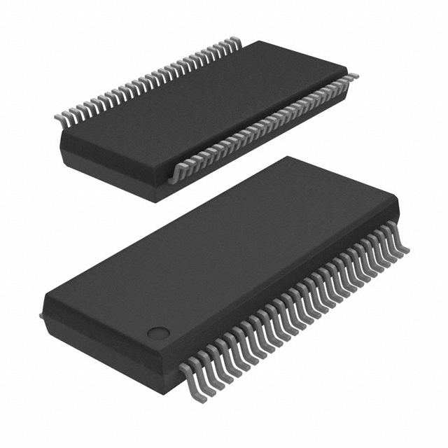


 工商网监
湘ICP备2023018690号
工商网监
湘ICP备2023018690号
