4-Output 1.8V PCIe Zero-Delay/Fanout
Clock Buffer with Zo = 100ohms
Description
Features/Benefits
• Direct connection to 100 transmission lines; saves 16
The 9DBV0441 is a member of Renesas’ SOC-Friendly
1.8V Very-Low-Power (VLP) PCIe family. It has integrated
output terminations providing Zo = 100 for direct
connection to 100 transmission lines. The device has 4
output enables for clock management, and 3 selectable
SMBus addresses.
•
•
•
•
Typical Applications
• 1.8V PCIe Gen1–5 Zero-Delay/Fan-out Buffer
•
(ZDB/FOB)
•
Output Features
• Four 1–200MHz Low-Power (LP) HCSL DIF pairs with
•
ZO = 100
•
Key Specifications
•
•
•
•
9DBV0441
Datasheet
•
DIF cycle-to-cycle jitter < 50ps
DIF output-to-output skew < 50ps
PCIe Gen5 CC additive phase jitter < 40fs RMS
12kHz–20MHz additive phase jitter = 156fs RMS at
156.25MHz (typical)
•
•
•
•
Block Diagram
resistors compared to standard HCSL outputs
53mW typical power consumption in PLL mode; minimal
power consumption
Spread Spectrum (SS) compatible; allows use of SS for
EMI reduction
OE# pins; support DIF power management
HCSL compatible differential input; can be driven by
common clock sources
Programmable Slew rate for each output; allows tuning
for various line lengths
Programmable output amplitude; allows tuning for
various application environments
Pin/software selectable PLL bandwidth and PLL Bypass;
minimize phase jitter for each application
Outputs blocked until PLL is locked; clean system
start-up
Software selectable 50MHz or 125MHz PLL operation;
useful for Ethernet applications
Configuration can be accomplished with strapping pins;
SMBus interface not required for device control
3.3V tolerant SMBus interface works with legacy
controllers
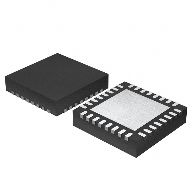
Space saving 5 × 5mm 32-VFQFPN; minimal board
space
Selectable SMBus addresses; multiple devices can
easily share an SMBus segment
vOE(3:0)#
DIF3
CLK_IN
ZDB PLL
CLK_IN#
DIF1
^SADR_tri
^vHIBW_BYPM_LOBW#
^CKPWRGD_PD#
SDATA_3.3
SCLK_3.3
DIF2
DIF0
CONTROL
LOGIC
©2021 Renesas Electronics Corporation
1
R31DS0072EU0800 July 29, 2021
�9DBV0441 Datasheet
VDDO1.8
GND
DIF3
DIF3#
vOE3#
GND
^CKPWRGD_PD#
^SADR_tri
Pin Configuration
32 31 30 29 28 27 26 25
^vHIBW_BYPM_LOBW# 1
24 vOE2#
23 DIF2#
FB_DNC 2
FB_DNC# 3
VDDR1.8 4
9DBV0441
CLK_IN 5
CLK_IN# 6
GNDR 7
GNDDIG 8
22 DIF2
21 VDDA1.8
20 GNDA
19 DIF1#
18 DIF1
17 vOE1#
VDDO1.8
GND
DIF0
DIF0#
vOE0#
SDATA_3.3
SCLK_3.3
VDDDIG1.8
9 10 11 12 13 14 15 16
32-pin VFQFPN, 5x5 mm, 0.5mm pitch
^ prefix indicates internal 120KOhm pull up resistor
^v prefix indicates internal 120KOhm pull up AND pull down resistor (biased to
VDD/2)
v prefix indicates internal 120KOhm pull down resistor
SMBus Address Selection Table
State of SADR on first application of
CKPWRGD_PD#
SADR
0
M
1
Address
1101011
1101100
1101101
+
Read/Write bit
x
x
x
Power Management Table
SMBus
DIFx
OEx# Pin
True O/P
Comp. O/P
OEx bit
0
X
X
X
Low
Low
1
Running
0
X
Low
Low
1
Running
1
0
Running
Running
1
Running
1
1
Low
Low
1. If Bypass mode is selected, the PLL will be off, and outputs will be running.
CKPWRGD_PD#
CLK_IN
©2021 Renesas Electronics Corporation
2
PLL
Off
On1
On1
On1
R31DS0072EU0800 July 29, 2021
�9DBV0441 Datasheet
Power Connections
Pin Number
VDD
GND
4
7
9
8
16, 25
15,20,26,30
21
20
Description
Input receiver analog
Digital Power
DIF outputs
PLL Analog
Frequency Select Table
FSEL
Byte3 [4:3]
00 (Default)
01
10
11
CLK_IN
(MHz)
100.00
50.00
125.00
Reserved
DIFx
(MHz)
CLK_IN
CLK_IN
CLK_IN
Reserved
PLL Operating Mode
HiBW_BypM_LoBW#
0
M
1
MODE
PLL Lo BW
Bypass
PLL Hi BW
Byte1 [7:6]
Readback
00
01
11
©2021 Renesas Electronics Corporation
Byte1 [4:3]
Control
00
01
11
3
R31DS0072EU0800 July 29, 2021
�9DBV0441 Datasheet
Pin Descriptions
Pin# Pin Name
1
2
3
4
5
6
7
8
9
10
11
12
13
14
15
16
17
18
19
20
21
22
23
24
25
26
27
28
29
30
31
32
Pin Description
Trilevel input to select High BW, Bypass or Low BW mode.
^vHIBW_BYPM_LOBW# LATCHED IN
See PLL Operating Mode Table for Details.
True clock of differential feedback. The feedback output and feedback input are
FB_DNC
DNC
connected internally on this pin. Do not connect anything to this pin.
Complement clock of differential feedback. The feedback output and feedback
FB_DNC#
DNC
input are connected internally on this pin. Do not connect anything to this pin.
1.8V power for differential input clock (receiver). This VDD should be treated as
VDDR1.8
PWR
an Analog power rail and filtered appropriately.
CLK_IN
IN
True Input for differential reference clock.
CLK_IN#
IN
Complementary Input for differential reference clock.
GNDR
GND
Analog Ground pin for the differential input (receiver)
GNDDIG
GND
Ground pin for digital circuitry
VDDDIG1.8
PWR
1.8V digital power (dirty power)
SCLK_3.3
IN
Clock pin of SMBus circuitry, 3.3V tolerant.
SDATA_3.3
I/O
Data pin for SMBus circuitry, 3.3V tolerant.
Active low input for enabling DIF pair 0. This pin has an internal pull-down.
vOE0#
IN
1 =disable outputs, 0 = enable outputs
DIF0
OUT
Differential true clock output
DIF0#
OUT
Differential Complementary clock output
GND
GND
Ground pin.
VDDO1.8
PWR
Power supply for outputs, nominally 1.8V.
Active low input for enabling DIF pair 1. This pin has an internal pull-down.
vOE1#
IN
1 =disable outputs, 0 = enable outputs
DIF1
OUT
Differential true clock output
DIF1#
OUT
Differential Complementary clock output
GNDA
GND
Ground pin for the PLL core.
VDDA1.8
PWR
1.8V power for the PLL core.
DIF2
OUT
Differential true clock output
DIF2#
OUT
Differential Complementary clock output
Active low input for enabling DIF pair 2. This pin has an internal pull-down.
vOE2#
IN
1 =disable outputs, 0 = enable outputs
VDDO1.8
PWR
Power supply for outputs, nominally 1.8V.
GND
GND
Ground pin.
DIF3
OUT
Differential true clock output
DIF3#
OUT
Differential Complementary clock output
Active low input for enabling DIF pair 3. This pin has an internal pull-down.
vOE3#
IN
1 =disable outputs, 0 = enable outputs
GND
GND
Ground pin.
Input notifies device to sample latched inputs and start up on first high assertion.
^CKPWRGD_PD#
IN
Low enters Power Down Mode, subsequent high assertions exit Power Down
Mode. This pin has internal pull-up resistor.
^SADR_tri
Type
LATCHED IN Tri-level latch to select SMBus Address. See SMBus Address Selection Table.
©2021 Renesas Electronics Corporation
4
R31DS0072EU0800 July 29, 2021
�9DBV0441 Datasheet
Test Loads
Low-Power HCSL Differential Output Test Load
5 inches
Rs
Zo=100ohm
2pF
Rs
2pF
Device
Driving LVDS
3.3V
Driving LVDS
Cc
R7a
R7b
R8a
R8b
Rs
Zo
Cc
Rs
Device
LVDS Clock
input
Driving LVDS inputs
Component
R7a, R7b
R8a, R8b
Cc
Vcm
Value
Receiver has Receiver does not
termination
have termination Note
10K ohm
140 ohm
5.6K ohm
75 ohm
0.1 uF
0.1 uF
1.2 volts
1.2 volts
©2021 Renesas Electronics Corporation
5
R31DS0072EU0800 July 29, 2021
�9DBV0441 Datasheet
Absolute Maximum Ratings
Stresses above the ratings listed below can cause permanent damage to the 9DBV0441. These ratings, which are standard
values for Renesas commercially rated parts, are stress ratings only. Functional operation of the device at these or any other
conditions above those indicated in the operational sections of the specifications is not implied. Exposure to absolute
maximum rating conditions for extended periods can affect product reliability. Electrical parameters are guaranteed only over
the recommended operating temperature range.
PARAMETER
SYMBOL
CONDITIONS
Supply Voltage
Input Voltage
Input High Voltage, SMBus
Storage Temperature
Junction Temperature
Input ESD protection
VDDx
V IN
V IHSMB
Ts
Tj
ESD prot
Applies to all VDD pins
MIN
-0.5
-0.5
TYP
SMBus clock and data pins
-65
Human Body Model
MAX
2.5
V DD+0.5V
3.6V
150
125
2000
UNITS NOTES
V
V
V
°C
°C
V
1,2
1, 3
1
1
1
1
1
Guaranteed by design and characterization, not 100% tested in production.
Operation under these conditions is neither implied nor guaranteed.
3
Not to exceed 2.5V.
2
Electrical Characteristics–Clock Input Parameters
TA = TCOM or TIND; Supply Voltage per VDD of normal operation conditions, See Test Loads for Loading Conditions
PARAMETER
SYMBOL
Input High Voltage - DIF_IN
V IHDIF
Input Low Voltage - DIF_IN
V ILDIF
CONDITIONS
Differential inputs
(single-ended measurement)
Differential inputs
(single-ended measurement)
MIN
TYP
MAX
UNITS NOTES
600
800
1150
mV
1
V SS - 300
0
300
mV
1,3
Input Common Mode
Voltage - DIF_IN
Input Amplitude - DIF_IN
Input Slew Rate - DIF_IN
Input Leakage Current
VCOM
Common Mode Input Voltage
300
725
mV
1
V SWING
dv/dt
IIN
Peak to Peak value (V IHDIF - V ILDIF)
Measured differentially
VIN = V DD , V IN = GND
300
0.4
-5
1450
5
mV
V/ns
uA
1
1,2
1
Input Duty Cycle
dtin
Measurement from differential waveform
45
55
%
1
Input Jitter - Cycle to Cycle
JDIFIn
Differential Measurement
0
150
ps
1
1
Guaranteed by design and characterization, not 100% tested in production.
2
Slew rate measured through +/-75mV window centered around differential zero.
3
The device can be driven from a single ended clock by driving the true clock and biasing the complement clock input to the V BIAS, where V BIAS
is (V IHHIGH - V IHLOW )/2.
©2021 Renesas Electronics Corporation
6
R31DS0072EU0800 July 29, 2021
�9DBV0441 Datasheet
Electrical Characteristics–Input/Supply/Common Parameters–Normal Operating
Conditions
TA = TCOM or TIND; Supply Voltage per VDD of normal operation conditions, See Test Loads for Loading Conditions
PARAMETER
SYMBOL
1.8V Supply Voltage
VDD
Ambient Operating
Temperature
TCOM
TIND
Input High Voltage
V IH
Input Mid Voltage
V IM
Single-ended tri-level inputs ('_tri' suffix)
Input Low Voltage
V IL
Single-ended inputs, except SMBus
IIN
IINP
Input Current
CONDITIONS
Supply voltage for core, analog and LVCMOS
outputs
Commercial range
MIN
TYP
MAX
UNITS NOTES
1.7
1.8
1.9
V
1
0
25
70
°C
1
Industrial range
-40
25
Single-ended inputs, except SMBus
0.75 VDD
85
°C
1
V DD + 0.3
V
1
0.4 V DD
0.6 V DD
V
1
-0.3
0.25 V DD
V
1
Single-ended inputs, V IN = GND, VIN = VDD
-5
5
uA
1
Single-ended inputs
V IN = 0 V; Inputs with internal pull-up resistors
-200
200
uA
1
V IN = VDD; Inputs with internal pull-down resistors
Input Frequency
Fiby p
Bypass mode
1
200
MHz
2
Fipll100
100MHz PLL mode
50
100.00
140
MHz
2
Fipll125
125MHz PLL mode
62.5
125.00
175
MHz
2
Fipll62
50MHz PLL mode
25
50.00
65
MHz
2
7
nH
1
Pin Inductance
Lpin
CIN
Logic Inputs, except DIF_IN
1.5
5
pF
1
Capacitance
CINDIF_IN
DIF_IN differential clock inputs
1.5
2.7
pF
1,6
6
pF
1
0.6
1
ms
1,2
31.500
33
kHz
1
3
clocks
1,3
300
us
1,3
5
ns
1,2
COUT
Clk Stabilization
TSTAB
Input SS Modulation
Frequency
fMODIN
OE# Latency
tLATOE#
Tdrive_PD#
t DRVPD
Tfall
tF
Output pin capacitance
From V DD Power-Up and after input clock
stabilization or de-assertion of PD# to 1st clock
Allowable Frequency
(Triangular Modulation)
DIF start after OE# assertion
DIF stop after OE# deassertion
DIF output enable after
PD# de-assertion
Fall time of single-ended control inputs
30
1
Trise
tR
Rise time of single-ended control inputs
5
ns
1,2
SMBus Input Low Voltage
V ILSMB
VDDSMB = 3.3V, see note 4 for VDDSMB < 3.3V
0.8
V
1, 4
SMBus Input High Voltage
VIHSMB
VDDSMB = 3.3V, see note 5 for VDDSMB < 3.3V
3.6
V
1, 5
SMBus Output Low Voltage
V OLSMB
@ IPULLUP
0.4
V
1
@ V OL
SMBus Sink Current
IPULLUP
Nominal Bus Voltage
V DDSMB
SCLK/SDATA Rise Time
tRSMB
SCLK/SDATA Fall Time
SMBus Operating
Frequency
tFSMB
fMAXSMB
2.1
4
mA
1
3.6
V
1
(Max VIL - 0.15) to (Min VIH + 0.15)
1000
ns
1
(Min VIH + 0.15) to (Max VIL - 0.15)
300
ns
1
Maximum SMBus operating frequency
400
kHz
1,7
1.7
1
Guaranteed by design and characterization, not 100% tested in production.
2
Control input must be monotonic from 20% to 80% of input swing.
3
Time from deassertion until outputs are > 200 mV.
For VDDSMB < 3.3V, V ILSMB < = 0.35V DDSMB.
5
For VDDSMB < 3.3V, V IHSMB > = 0.65VDDSMB.
4
6
DIF_IN input.
7
The differential input clock must be running for the SMBus to be active.
©2021 Renesas Electronics Corporation
7
R31DS0072EU0800 July 29, 2021
�9DBV0441 Datasheet
Electrical Characteristics–DIF 0.7V Low Power HCSL Outputs
TA = TCOM or TIND; Supply Voltage per VDD of normal operation conditions, See Test Loads for Loading Conditions
PARAMETER
SYMBOL
Slew rate
Trf
Slew rate matching
ΔTrf
Voltage High
VHIGH
Voltage Low
VLOW
CONDITIONS
MIN
TYP
Scope averaging on 3.0V/ns setting
Scope averaging on 2.0V/ns setting
Slew rate matching, Scope averaging on
1.1
1.9
2
3
7
3
4
20
Statistical measurement on single-ended signal
using oscilloscope math function. (Scope
averaging on)
660
774
850
-150
18
150
821
-15
1536
414
13
1150
-300
300
250
Measurement on single ended signal using
Vmax
absolute value. (Scope averaging off)
Vmin
Vswing
Scope averaging off
Vcross_abs
Scope averaging off
Scope averaging off
Δ-Vcross
1
Guaranteed by design and characterization, not 100% tested in production.
2
Measured from differential waveform
Max Voltage
Min Voltage
Vswing
Crossing Voltage (abs)
Crossing Voltage (var)
MAX UNITS NOTES
550
140
V/ns
V/ns
%
1, 2, 3
1, 2, 3
1, 2, 4
1,7
mV
1,7
1
1
1,2,7
1,5,7
1, 6
mV
mV
mV
mV
3
Slew rate is measured through the Vswing voltage range centered around differential 0V. This results in a +/-150mV window around
differential 0V.
4
Matching applies to rising edge rate for Clock and falling edge rate for Clock#. It is measured using a +/-75mV window centered on
the average cross point where Clock rising meets Clock# falling. The median cross point is used to calculate the voltage thresholds the
oscilloscope is to use for the edge rate calculations.
5
Vcross is defined as voltage where Clock = Clock# measured on a component test board and only applies to the differential rising
edge (i.e. Clock rising and Clock# falling).
6
The total variation of all Vcross measurements in any particular system. Note that this is a subset of Vcross_min/max (Vcross
absolute) allowed. The intent is to limit Vcross induced modulation by setting Δ- Vcross to be smaller than Vcross absolute.
7
At default SMBus settings.
Electrical Characteristics–Current Consumption
TA = TCOM or TIND; Supply Voltage per VDD of normal operation conditions, See Test Loads for Loading Conditions
PARAMETER
Operating Supply Current
Powerdown Current
SYMBOL
CONDITIONS
MIN
TYP
MAX
UNITS
NOTES
IDDAOP
VDDA+VDDR, PLL Mode, @100MHz
11
15
mA
1
IDDOP
VDD1.8, All outputs active @100MHz
25
35
mA
1
IDDAPD
VDDA+VDDR, PLL Mode, @100MHz
1
mA
1,2
IDDPD
VDD1.8, Outputs Low/Low
1.2
mA
1, 2
1
Guaranteed by design and characterization, not 100% tested in production.
2
Input clock stopped.
©2021 Renesas Electronics Corporation
8
R31DS0072EU0800 July 29, 2021
�9DBV0441 Datasheet
Electrical Characteristics–Output Duty Cycle, Jitter, Skew and PLL Characteristics
TA = TCOM or TIND; Supply Voltage per VDD of normal operation conditions, See Test Loads for Loading Conditions
PARAMETER
SYMBOL
CONDITIONS
MIN
TYP
MAX
UNITS
NOTES
2
1
45
2.7
1.4
1.2
50.1
4
2
2
55
MHz
MHz
dB
%
1,5
1,5
1
1
PLL Bandwidth
BW
PLL Jitter Peaking
Duty Cycle
t JPEAK
t DC
-3dB point in High BW Mode
-3dB point in Low BW Mode
Peak Pass band Gain
Measured differentially, PLL Mode
Duty Cycle Distortion
t DCD
Measured differentially, Bypass Mode @100MHz
-1
0
1
%
1,3
Jitter, Cycle to cycle
t jcyc-cyc
Bypass Mode, VT = 50%
PLL Mode V T = 50%
V T = 50%
PLL mode
Additive Jitter in Bypass Mode
3000
0
Skew, Output to Output
t pdBYP
t pdPLL
t sk3
3600
92
28
16
0.1
4500
200
50
50
25
ps
ps
ps
ps
ps
1
1,4
1,4
1,2
1,2
Skew, Input to Output
1
Guaranteed by design and characterization, not 100% tested in production.
2
Measured from differential waveform
3
Duty cycle distortion is the difference in duty cycle between the output and the input clock when the device is operated in bypass mode.
4
All outputs at default slew rate
5
The MIN/TYP/MAX values of each BW setting track each other, i.e., Low BW MAX will never occur with Hi BW MIN.
Electrical Characteristics–Phase Jitter Parameters – 12kHz to 20MHz
TAMB = over the specified operating range. Supply Voltages per normal operation conditions. See Test Loads for loading conditions.
Parameter
Symbol
Conditions
Minimum
Typical
Maximum
12k-20M Additive Phase Jitter,
Fan-out Buffer Mode,
tjph12k-20MFOB
156
Fan-out Buffer Mode
SSC OFF, 156.25MHz
Notes:
1. Applies to all differential outputs, guaranteed by design and characterization. See Test Loads for measurement setup details.
2. 12kHz to 20MHz brick wall filter.
2
Specification
Limit
Units
Notes
n/a
fs
(rms)
1, 2, 3
2
3. For RMS values additive jitter is calculated by solving for b where [b = sqrt(c - a )], a is rms input jitter and c is rms total jitter.
©2021 Renesas Electronics Corporation
9
R31DS0072EU0800 July 29, 2021
�9DBV0441 Datasheet
Electrical Characteristics–Additive PCIe Phase Jitter for Fanout Buffer Mode[7]
T AMB = over the specified operating range. Supply Voltages per normal operation conditions. See Test Loads for loading conditions.
Parameter
Symbol
Conditions
Minimum Typical Maximum
Limit
tjphPCIeG1-CC
PCIe Gen 1 (2.5 GT/s)
1.7
3.0
86
PCIe Gen 2 Hi Band (5.0 GT/s)
0.033
0.049
3
PCIe Gen 2 Lo Band (5.0 GT/s)
0.122
0.199
3.1
tjphPCIeG3-CC
PCIe Gen 3 (8.0 GT/s)
0.059
0.098
1
tjphPCIeG4-CC
PCIe Gen 4 (16.0 GT/s)
0.059
0.098
0.5
tjphPCIeG5-CC
PCIe Gen 5 (32.0 GT/s)
0.023
0.038
0.15
tjphPCIeG1-SRIS
PCIe Gen 1 (2.5 GT/s)
0.175
0.038
n/a
tjphPCIeG2-SRIS
PCIe Gen 2 (5.0 GT/s)
0.156
0.275
n/a
tjphPCIeG3-SRIS
PCIe Gen 3 (8.0 GT/s)
0.041
0.247
n/a
tjphPCIeG4-SRIS
PCIe Gen 4 (16.0 GT/s)
0.043
0.064
n/a
tjphPCIeG5-SRIS
PCIe Gen 5 (32.0 GT/s)
0.036
0.066
n/a
tjphPCIeG2-CC
Additive PCIe Phase Jitter,
Fan-out Buffer Mode
(Common Clocked Architecture)
Additive PCIe Phase Jitter,
Fan-out Buffer Mode
(SRIS Architecture)
Units
ps
(p-p)
ps
(RMS)
ps
(RMS)
ps
(RMS)
ps
(RMS)
ps
(RMS)
ps
(RMS)
ps
(RMS)
ps
(RMS)
ps
(RMS)
ps
(RMS)
Notes
1, 2
1, 2
1, 2
1, 2
1, 2, 3, 4
1, 2, 3, 5
1, 2, 6
1, 2, 6
1, 2, 6
1, 2, 6
1, 2, 6
Notes:
1. The Refclk jitter is measured after applying the filter functions found in PCI Express Base Specification 5.0, Revision 1.0. See the Test Loads section of the data sheet
for the exact measurement setup. The total Ref Clk jitter limits for each data rate are listed for convenience. The worst case results for each data rate are summarized in
this table. If oscilloscope data is used, equipment noise is removed from all results.
2. Jitter measurements shall be made with a capture of at least 100,000 clock cycles captured by a real-time oscilloscope (RTO) with a sample rate of 20 GS/s or
greater. Broadband oscilloscope noise must be minimized in the measurement. The measured PP jitter is used (no extrapolation) for RTO measurements. Alternately Jitter measurements may be used with a Phase Noise Analyzer (PNA) extending (flat) and integrating and folding the frequency content up to an offset from the carrier
frequency of at least 200 MHz (at 300 MHz absolute frequency) below the Nyquist frequency. For PNA measurements for the 2.5 GT/s data rate, the RMS jitter is
converted to peak to peak jitter using a multiplication factor of 8.83. In the case where real-time oscilloscope and PNA measurements have both been done and produce
different results the RTO result must be used.
3. SSC spurs from the fundamental and harmonics are removed up to a cutoff frequency of 2 MHz taking care to minimize removal of any non-SSC content.
4. Note that 0.7 ps RM S is to be used in channel simulations to account for additional noise in a real system.
5. Note that 0.25 ps RMS is to be used in channel simulations to account for additional noise in a real system.
6. The PCI Express Base Specification 5.0, Revision 1.0 provides the filters necessary to calculate SRIS jitter values, however, it does not provide specification limits,
hence the n/a in the Limit column. SRIS values are informative only. In general, a clock operating in an SRIS system must be twice as good as a clock operating in a
Common Clock system. For RM S values, twice as good is equivalent to dividing the CC value by 2. And additional consideration is the value for which to divide by 2.
The conservative approach is to divide the ref clock jitter limit, and the case can be made for dividing the channel simulation values by 2, if the ref clock is close to the Tx
clock input. An example for Gen4 is as follows. A "rule-of-thumb" SRIS limit would be either 0.5ps RMS/2 = 0.35ps RMS if the clock chip is far from the clock input, or
0.7ps RMS/ 2 = 0.5ps RM S if the clock chip is near the clock input..
7. Additive jitter for RMS values is calculated by solving for b where b
©2021 Renesas Electronics Corporation
𝑎2 , and a is rms input jitter and c is rms output jitter.
√ 𝑐2
10
R31DS0072EU0800 July 29, 2021
�9DBV0441 Datasheet
Additive Phase Jitter Plot: 125M (12kHz to 20MHz)
©2021 Renesas Electronics Corporation
11
R31DS0072EU0800 July 29, 2021
�9DBV0441 Datasheet
General SMBus Serial Interface Information
How to Write
•
•
How to Read
•
•
•
•
•
•
•
•
•
•
•
Controller (host) sends a start bit
Controller (host) sends the write address
Renesas clock will acknowledge
Controller (host) sends the beginning byte location = N
Renesas clock will acknowledge
Controller (host) sends the byte count = X
Renesas clock will acknowledge
Controller (host) starts sending Byte N through Byte
N+X-1
Renesas clock will acknowledge each byte one at a
time
Controller (host) sends a Stop bit
•
•
•
Controller (host) will send a start bit
Controller (host) sends the write address
Renesas clock will acknowledge
Controller (host) sends the beginning byte location = N
Renesas clock will acknowledge
Controller (host) will send a separate start bit
Controller (host) sends the read address
Renesas clock will acknowledge
Renesas clock will send the data byte count = X
Renesas clock sends Byte N+X-1
Renesas clock sends Byte 0 through Byte X (if X(H)
was written to Byte 8)
Controller (host) will need to acknowledge each byte
Controller (host) will send a not acknowledge bit
Controller (host) will send a stop bit
Index Block Write Operation
Renesas (Slave/Receiver)
Index Block Read Operation
Controller (Host)
Renesas (Slave/Receiver)
Controller (Host)
T
starT bit
T
Slave Address
WR
Slave Address
WRite
WR
ACK
Beginning Byte = N
ACK
ACK
Data Byte Count = X
RT
ACK
X Byte
O
O
O
O
RD
Data Byte Count=X
ACK
Beginning Byte N
Byte N + X - 1
ACK
ACK
O
stoP bit
O
O
O
O
O
Note: SMBus Address is Latched on SADR pin.
©2021 Renesas Electronics Corporation
ReaD
ACK
O
P
Repeat starT
Slave Address
ACK
O
WRite
ACK
Beginning Byte = N
Beginning Byte N
starT bit
12
N
Not acknowledge
P
stoP bit
X Byte
•
•
•
•
•
•
•
•
Byte N + X - 1
R31DS0072EU0800 July 29, 2021
�9DBV0441 Datasheet
SMBus Table: Output Enable Register 1
Byte 0
Name
Control Function
Type
0
Reserved
Bit 7
DIF OE3
Output Enable
RW
Low/Low
Bit 6
DIF OE2
Output Enable
RW
Low/Low
Bit 5
Reserved
Bit 4
DIF OE1
Output Enable
RW
Low/Low
Bit 3
Reserved
Bit 2
DIF OE0
Output Enable
RW
Low/Low
Bit 1
Reserved
Bit 0
1. A low on these bits will override the OE# pin and force the differential output Low/Low
SMBus Table: PLL Operating Mode and Output Amplitude Control Register
Byte 1
Name
Control Function
Type
PLLMODERB1
PLL Mode Readback Bit 1
Bit 7
R
PLLMODERB0
PLL Mode Readback Bit 0
Bit 6
R
Bit 5
PLLMODE_SWCNTRL
Enable SW control of PLL Mode RW
PLLMODE1
PLL Mode Control Bit 1
Bit 4
PLLMODE0
PLL Mode Control Bit 0
Bit 3
Reserved
Bit 2
AMPLITUDE 1
Bit 1
Controls Output Amplitude
AMPLITUDE 0
Bit 0
1. B1[5] must be set to a 1 for these bits to have any effect on the part.
SMBus Table: DIF Slew Rate Control Register
Byte 2
Name
Control Function
Reserved
Bit 7
SLEWRATESEL DIF3
Slew Rate Selection
Bit 6
SLEWRATESEL DIF2
Slew Rate Selection
Bit 5
Reserved
Bit 4
SLEWRATESEL DIF1
Slew Rate Selection
Bit 3
Reserved
Bit 2
SLEWRATESEL DIF0
Slew Rate Selection
Bit 1
Reserved
Bit 0
SMBus Table: Frequency Select Control Register
Byte 3
Name
Control Function
Reserved
Bit 7
Reserved
Bit 6
Enable SW selection of
FREQ_SEL_EN
Bit 5
frequency
FSEL1
Freq. Select Bit 1
Bit 4
FSEL0
Freq. Select Bit 0
Bit 3
Reserved
Bit 2
Reserved
Bit 1
SLEWRATESEL FB
Adjust Slew Rate of FB
Bit 0
1. B3[5] must be set to a 1 for these bits to have any effect on the part.
1
1
Enabled
Enabled
Enabled
Enabled
0
1
See PLL Operating Mode Table
Values in B1[7:6]
set PLL Mode
Values in B1[4:3]
set PLL Mode
RW
RW 1
See PLL Operating Mode Table
RW
RW
00 = 0.6V
10= 0.8V
01 = 0.7V
11 = 0.9V
Type
0
1
RW
RW
2 V/ns
2 V/ns
3 V/ns
3 V/ns
RW
2 V/ns
3 V/ns
RW
2 V/ns
3 V/ns
Type
0
1
RW
SW frequency
change disabled
SW frequency
change enabled
RW 1
RW
1
RW
See Frequency Select Table
2V/ns
3V/ns
Default
1
1
1
1
1
1
1
1
Default
Latch
Latch
0
0
0
1
1
0
Default
1
1
1
1
1
1
1
1
Default
1
1
0
0
0
1
1
1
Byte 4 is Reserved and reads back 'hFF
©2021 Renesas Electronics Corporation
13
R31DS0072EU0800 July 29, 2021
�9DBV0441 Datasheet
SMBus Table: Revision and Vendor ID Register
Byte 5
Name
Control Function
RID3
Bit 7
RID2
Bit 6
Revision ID
RID1
Bit 5
RID0
Bit 4
VID3
Bit 3
VID2
Bit 2
VENDOR ID
VID1
Bit 1
VID0
Bit 0
Type
R
R
R
R
R
R
R
R
SMBus Table: Device Type/Device ID
Byte 6
Name
Device Type1
Bit 7
Device Type0
Bit 6
Device ID5
Bit 5
Device ID4
Bit 4
Device ID3
Bit 3
Device ID2
Bit 2
Device ID1
Bit 1
Device ID0
Bit 0
Type
R
R
R
R
R
R
R
R
SMBus Table: Byte Count Register
Byte 7
Name
Bit 7
Bit 6
Bit 5
BC4
Bit 4
BC3
Bit 3
BC2
Bit 2
BC1
Bit 1
BC0
Bit 0
©2021 Renesas Electronics Corporation
Control Function
Device Type
Device ID
Control Function
Reserved
Reserved
Reserved
Byte Count Programming
14
Type
RW
RW
RW
RW
RW
0
1
A rev = 0000
0001 = IDT
0
1
00 = FGV, 01 = DBV,
10 = DMV, 11= Reserved
000100 binary or 04 hex
0
Default
0
0
0
0
0
0
0
1
Default
0
1
0
0
0
1
0
0
1
Default
0
0
0
0
Writing to this register will configure how
1
many bytes will be read back, default is
0
= 8 bytes.
0
0
R31DS0072EU0800 July 29, 2021
�9DBV0441 Datasheet
Marking Diagrams
ICS
BV0441AL
YYWW
COO
LOT
ICS
B0441AIL
YYWW
COO
LOT
Notes:
1. “LOT” is the lot sequence number.
2. “COO” denotes country of origin.
3. YYWW is the last two digits of the year and week that the part was assembled.
4. Line 2: truncated part number
5. “L” denotes RoHS compliant package.
6. “I” denotes industrial temperature range device.
Thermal Characteristics
1
PARAMETER
SYMBOL
Thermal Resistance
θJC
θJb
θJA0
θJA1
θJA3
θJA5
TYP
VALUE
Junction to Case
42
Junction to Base
2.4
Junction to Air, still air
39
NLG32
Junction to Air, 1 m/s air flow
33
Junction to Air, 3 m/s air flow
28
Junction to Air, 5 m/s air flow
27
CONDITIONS
PKG
UNITS NOTES
°C/W
°C/W
°C/W
°C/W
°C/W
°C/W
1
1
1
1
1
1
ePad soldered to board
©2021 Renesas Electronics Corporation
15
R31DS0072EU0800 July 29, 2021
�9DBV0441 Datasheet
Package Outline Drawings
The package outline drawings are appended at the end of this document and are accessible from the link below. The
package information is the most current data available.
32-VFQFPN (NLG32P1
Ordering Information
Part / Order Number Shipping Packaging
9DBV0441AKLF
Trays
9DBV0441AKLFT
Tape and Reel
9DBV0441AKILF
Trays
9DBV0441AKILFT
Tape and Reel
Package
32-pin VFQFPN
32-pin VFQFPN
32-pin VFQFPN
32-pin VFQFPN
Temperature
0 to +70° C
0 to +70° C
-40 to +85° C
-40 to +85° C
“LF” suffix to the part number are the Pb-Free configuration and are RoHS compliant.
“A” is the device revision designator (will not correlate with the datasheet revision).
Revision History
Revision Date
August 13, 2012
February 25, 2013
October 27, 2014
November 26, 2014
April 22, 2016
August 27, 2019
July 29, 2020
July 29, 2021
Description
1. Removed "Differential" from DS title and Recommended Application, corrected typo's in
Description. Updated block diagram to indicate internal terminations.
2. Corrected spelling error in pull-up/pulldown text under pinout
3. Updated all electrical tables and added "Industry Limit" column to "Phase Jitter
Parameters".
4. Updated Byte3[0] to be consistent with Byte 2. Updated Byte6[7:6] definition.
5. Added thermal data to page 12.
6. Added NLG32 to "Package Outline and Package Dimensions" on page 13.
7. Move to final.
1. Changed VIH min. from 0.65*VDD to 0.75*VDD
2. Changed VIL max. from 0.35*VDD to 0.25*VDD
3. Added missing mid-level input voltage spec (VIM) of 0.4*VDD to 0.6*VDD.
1. Updated front page text for consistency and updated block diagram resistor colors to
highlight internal resistors.
2. Updated max frequency of 100MHz PLL mode from 110MHz to 140MHz
3. Updated max frequency of 125MHz PLL mode from 137.5MHz to 175MHz
4. Updated max frequency of 50MHz PLL mode from 55MHz to 65MHz
1. Updated Key Specifications with additive phase jitter.
2. Added additive phase jitter plot to specifications.
1. Updated max frequency of 100MHz PLL mode to 140MHz
2. Updated max frequency of 125MHz PLL mode to 175MHz
3. Updated max frequency of 50MHz PLL mode to 65MHz
Update to PCIe Gen4.
Corrected typo in Output Features on front page; changed 200Hz to 200MHz.
1. Updated document title.
2. Updated Recommended Applications.
3. Updated Key Specifications.
4. Updated Phase Jitter tables.
©2021 Renesas Electronics Corporation
16
R31DS0072EU0800 July 29, 2021
�32-VFQFPN, Package Outline Drawing
5.0 x 5.0 x 0.90 mm Body, Epad 3.15 x 3.15 mm.
NLG32P1, PSC-4171-01, Rev 02, Page 1
�32-VFQFPN, Package Outline Drawing
5.0 x 5.0 x 0.90 mm Body, Epad 3.15 x 3.15 mm.
NLG32P1, PSC-4171-01, Rev 02, Page 2
Package Revision History
Description
Date Created
Rev No.
April 12, 2018
Rev 02
New Format
Feb 8, 2016
Rev 01
Added "k: Value
�IMPORTANT NOTICE AND DISCLAIMER
RENESAS ELECTRONICS CORPORATION AND ITS SUBSIDIARIES (“RENESAS”) PROVIDES TECHNICAL
SPECIFICATIONS AND RELIABILITY DATA (INCLUDING DATASHEETS), DESIGN RESOURCES (INCLUDING
REFERENCE DESIGNS), APPLICATION OR OTHER DESIGN ADVICE, WEB TOOLS, SAFETY INFORMATION, AND
OTHER RESOURCES “AS IS” AND WITH ALL FAULTS, AND DISCLAIMS ALL WARRANTIES, EXPRESS OR IMPLIED,
INCLUDING, WITHOUT LIMITATION, ANY IMPLIED WARRANTIES OF MERCHANTABILITY, FITNESS FOR A
PARTICULAR PURPOSE, OR NON-INFRINGEMENT OF THIRD PARTY INTELLECTUAL PROPERTY RIGHTS.
These resources are intended for developers skilled in the art designing with Renesas products. You are solely responsible
for (1) selecting the appropriate products for your application, (2) designing, validating, and testing your application, and (3)
ensuring your application meets applicable standards, and any other safety, security, or other requirements. These
resources are subject to change without notice. Renesas grants you permission to use these resources only for
development of an application that uses Renesas products. Other reproduction or use of these resources is strictly
prohibited. No license is granted to any other Renesas intellectual property or to any third party intellectual property.
Renesas disclaims responsibility for, and you will fully indemnify Renesas and its representatives against, any claims,
damages, costs, losses, or liabilities arising out of your use of these resources. Renesas' products are provided only subject
to Renesas' Terms and Conditions of Sale or other applicable terms agreed to in writing. No use of any Renesas resources
expands or otherwise alters any applicable warranties or warranty disclaimers for these products.
(Rev.1.0 Mar 2020)
Corporate Headquarters
Contact Information
TOYOSU FORESIA, 3-2-24 Toyosu,
Koto-ku, Tokyo 135-0061, Japan
www.renesas.com
For further information on a product, technology, the most
up-to-date version of a document, or your nearest sales
office, please visit:
www.renesas.com/contact/
Trademarks
Renesas and the Renesas logo are trademarks of Renesas
Electronics Corporation. All trademarks and registered
trademarks are the property of their respective owners.
© 2020 Renesas Electronics Corporation. All rights reserved.
�


 工商网监
湘ICP备2023018690号
工商网监
湘ICP备2023018690号
