DATASHEET
Programmable Timing Control HubTM for Intel Systems
Features/Benefits:
•
Supports tight ppm accuracy clocks for Serial-ATA and
PCI-Express
•
Supports spread spectrum modulation, 0 to -0.5%
down spread
Recommended Application:
I-temp CK410 clock, Intel Yellow Cover part
Output Features:
•
2 - 0.7V current-mode differential CPU pairs
•
6 - 0.7V current-mode differential SRC pair for SATA and
PCI-E
•
1 - 0.7V current-mode differential CPU/SRC selectable
pair
•
6 - PCI (33MHz)
•
3 - PCICLK_F, (33MHz) free-running
•
1 - USB, 48MHz
•
1 - DOT, 96MHz, 0.7V current differential pair
•
1 - REF, 14.318MHz
2
0
0
1
1
0
0
1
1
0
1
0
1
0
1
0
1
CPU
MHz
266.66
133.33
200.00
SRC
MHz
100.00
100.00
100.00
100.00
100.00
PCI
REF
MHz
MHz
33.33
14.318
33.33
14.318
33.33
14.318
RESERVED
RESERVED
33.33
14.318
RESERVED
RESERVED
USB
MHz
48.00
48.00
48.00
DOT
MHz
96.00
96.00
96.00
48.00
96.00
•
Uses external 14.318MHz crystal, external crystal load
caps are required for frequency tuning
•
Supports undriven differential CPU, SRC pair in PD#
for power management.
1. FS_C is a three-level input. Please see V IL_FS and V IH_FS specifications in
the Input/Supply/Common Output Parameters Table for correct values.
Also refer to the Test Clarification Table.
2. FS_B and FS_A are low-threshold inputs. Please see the V IL_FS and VIH_FS
specifications in the Input/Supply/Common Output Parameters Table for correct values.
1
2
3
4
5
6
7
8
9
10
11
12
13
14
15
16
17
18
19
20
21
22
23
24
25
26
27
28
ICS9E4101
0
0
0
0
1
1
1
1
2
FS_B FS_A
Supports CPU clks up to 400MHz
VDDPCI
GND
PCICLK3
PCICLK4
PCICLK5
GND
VDDPCI
ITP_EN/PCICLK_F0
PCICLK_F1
PCICLK_F2
VDD48
USB_48MHz
GND
DOTT_96MHz
DOTC_96MHz
FS_B/TEST_MODE
Vtt_PwrGd#/PD
FS_A_410
SRCCLKT1
SRCCLKC1
VDDSRC
SRCCLKT2
SRCCLKC2
SRCCLKT3
SRCCLKC3
SRCCLKT4_SATA
SRCCLKC4_SATA
VDDSRC
Functionality
1
•
Pin Configuration
Key Specifications:
•
CPU outputs cycle-cycle jitter < 85ps
•
SRC output cycle-cycle jitter = 2.0V to select TEST
o Power-up w/ V < 2.0V to have pin function as
FS_C.
· When pin is FS_C, VIH_FS and VIL_FS levels
apply.
· FS_B/TEST_MODE is a low-threshold input
o VIH_FS and VIL_FS levels apply.
o TEST_MODE is a real time input
· TEST_SEL can be invoked after power up through
SMBus B6b6.
o If TEST is selected by B6b6, only B6b7 controls
TEST_MODE. The FS_B/TEST_Mode pin is not
used.
· Power must be cycled to exit TEST.
SW
TEST
FS_C/TEST FS_B/TEST ENTRY
BIT
_SEL
_MODE
HW PIN HW PIN
B6b6
0
X
0
1
0
X
1
0
X
1
1
X
REF/N or
HI-Z
B6b7
OUTPUT
X
NORMAL
0
HI-Z
1
REF/N
0
REF/N
1
1
X
1
REF/N
0
X
1
0
HI-Z
0
X
1
1
REF/N
B6b6: 1= ENTER TEST MODE, Default = 0 (NORMAL OPERATION)
B6b7: 1= REF/N, Default = 0 (HI-Z)
IDTTM Programmable Timing Control HubTM for Intel Systems
1408A—01/25/10
17
�ICS9E4101
Programmable Timing Control HubTM for Intel Systems
c
N
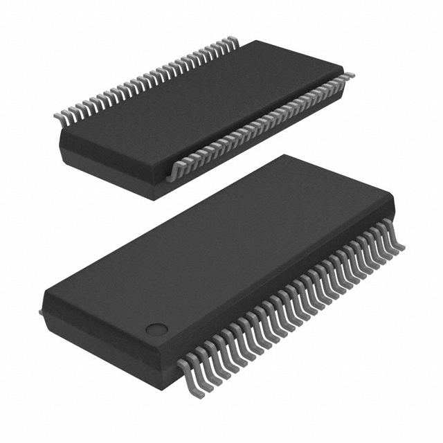
56-Lead, 300 mil Body, 25 mil, SSOP
L
E1
INDEX
AREA
E
1 2
α
h x 45°
D
A
A1
A
A1
b
c
D
E
E1
e
h
L
N
a
In Millimeters
COMMON DIMENSIONS
MIN
MAX
2.41
2.80
0.20
0.40
0.20
0.34
0.13
0.25
SEE VARIATIONS
10.03
10.68
7.40
7.60
0.635 BASIC
0.38
0.64
0.50
1.02
SEE VARIATIONS
0°
8°
In Inches
COMMON DIMENSIONS
MIN
MAX
.095
.110
.008
.016
.008
.0135
.005
.010
SEE VARIATIONS
.395
.420
.291
.299
0.025 BASIC
.015
.025
.020
.040
SEE VARIATIONS
0°
8°
VARIATIONS
-C-
e
SYMBOL
SEATING
PLANE
b
N
56
D mm.
MIN
18.31
D (inch)
MAX
18.55
MIN
.720
MAX
.730
.10 (.004) C
Reference Doc.: JEDEC Publication 95, MO-118
10-0034
Ordering Information
9E4101yFILFT
Example:
XXXX y F I LF T
Designation for tape and reel packaging
Lead Free, RoHS Compliant
Industrial Temperature Range
Package Type
F = SSOP
Revision Designator (will not correlate with datasheet revision)
Device Type
IDTTM Programmable Timing Control HubTM for Intel Systems
1408A—01/25/10
18
�ICS9E4101
Programmable Timing Control HubTM for Intel Systems
Revision History
Rev.
0.1
Issue Date
10/25/07
0.2
07/11/08
0.3
0.4
0.5
A
10/06/08
01/07/09
02/17/09
01/25/10
Description
Initial Release
Corrected operating temperature range on "Absolute Max" electrical
characteristics table.
Corrected typo on ordering information.
Removed "Advanced Information" from document header.
Added thermal chars.
Released to final. Updated document template.
Page #
12
19
Various
12
Innovate with IDT and accelerate your future networks. Contact:
www.IDT.com
TM
For Sales
For Tech Support
800-345-7015
408-284-8200
Fax: 408-284-2775
408-284-6578
pcclockhelp@idt.com
Corporate Headquarters
Asia Pacific and Japan
Europe
Integrated Device Technology, Inc.
6024 Silver Creek Valley Road
San Jose, CA 95138
United States
800 345 7015
+408 284 8200 (outside U.S.)
Integrated Device Technology
Singapore (1997) Pte. Ltd.
Reg. No. 199707558G
435 Orchard Road
#20-03 Wisma Atria
Singapore 238877
+65 6 887 5505
IDT Europe, Limited
Prime House
Barnett Wood Lane
Leatherhead, Surrey
United Kingdom KT22 7DE
+44 1372 363 339
© 2009 Integrated Device Technology, Inc. All rights reserved. Product specifications subject to change without notice. IDT, ICS, and the IDT logo are trademarks
of Integrated Device Technology, Inc. Accelerated Thinking is a service mark of Integrated Device Technology, Inc. All other brands, product names and marks
are or may be trademarks or registered trademarks used to identify products or services of their respective owners.
Printed in USA
19
�IMPORTANT NOTICE AND DISCLAIMER
RENESAS ELECTRONICS CORPORATION AND ITS SUBSIDIARIES (“RENESAS”) PROVIDES TECHNICAL
SPECIFICATIONS AND RELIABILITY DATA (INCLUDING DATASHEETS), DESIGN RESOURCES (INCLUDING
REFERENCE DESIGNS), APPLICATION OR OTHER DESIGN ADVICE, WEB TOOLS, SAFETY INFORMATION, AND
OTHER RESOURCES “AS IS” AND WITH ALL FAULTS, AND DISCLAIMS ALL WARRANTIES, EXPRESS OR IMPLIED,
INCLUDING, WITHOUT LIMITATION, ANY IMPLIED WARRANTIES OF MERCHANTABILITY, FITNESS FOR A
PARTICULAR PURPOSE, OR NON-INFRINGEMENT OF THIRD PARTY INTELLECTUAL PROPERTY RIGHTS.
These resources are intended for developers skilled in the art designing with Renesas products. You are solely responsible
for (1) selecting the appropriate products for your application, (2) designing, validating, and testing your application, and (3)
ensuring your application meets applicable standards, and any other safety, security, or other requirements. These
resources are subject to change without notice. Renesas grants you permission to use these resources only for
development of an application that uses Renesas products. Other reproduction or use of these resources is strictly
prohibited. No license is granted to any other Renesas intellectual property or to any third party intellectual property.
Renesas disclaims responsibility for, and you will fully indemnify Renesas and its representatives against, any claims,
damages, costs, losses, or liabilities arising out of your use of these resources. Renesas' products are provided only subject
to Renesas' Terms and Conditions of Sale or other applicable terms agreed to in writing. No use of any Renesas resources
expands or otherwise alters any applicable warranties or warranty disclaimers for these products.
(Rev.1.0 Mar 2020)
Corporate Headquarters
Contact Information
TOYOSU FORESIA, 3-2-24 Toyosu,
Koto-ku, Tokyo 135-0061, Japan
www.renesas.com
For further information on a product, technology, the most
up-to-date version of a document, or your nearest sales
office, please visit:
www.renesas.com/contact/
Trademarks
Renesas and the Renesas logo are trademarks of Renesas
Electronics Corporation. All trademarks and registered
trademarks are the property of their respective owners.
© 2020 Renesas Electronics Corporation. All rights reserved.
�


 工商网监
湘ICP备2023018690号
工商网监
湘ICP备2023018690号
