ICS9LPRS511
Advance Information
Integrated
Circuit
Systems, Inc.
Low Power Programmable Timing Control Hub™ for P4™ processor
Recommended Application:
Low Power CK505 Programmable clock
Features/Benefits:
•
Programmable output frequencies
•
Programmable output skew.
•
Programmable spread percentage for EMI control.
•
Programmable watch dog safe frequency.
•
Supports tight ppm accuracy clocks for Serial-ATA
•
Supports spread spectrum modulation, ±0.25% center
spread.
Output Features:
•
2 - 0.8V differential push-pull CPU pairs
•
1 - 25 MHz
•
5 - PCI (33MHz)
•
1 - USB, 48MHz
•
1 - 24/48MHz
•
1 - REF, 14.318MHz
•
8 - PCIEX 0.8V differential push-pull pairs
•
1 - PCIEX/DOT96MHz selectable pairs
•
1 - SATACLK differential pair
•
1 - 24.576MHz output
•
Uses external 14.318MHz crystal, external crystal load
caps are required for frequency tuning
•
Low Power differential outputs (50ohm resistor to GND
not needed)
•
Integrated 33Ω series resistor on all differential
outputs
Key Specifications:
•
CPU outputs cycle-cycle jitter < 85ps
•
PCIEX outputs cycle-cycle jitter < 125ps
•
PCI outputs cycle-cycle jitter < 250ps
•
+/- 300ppm frequency accuracy on CPU & PCIEX clocks
Bit4
Bit3
0
0
0
0
0
0
0
0
0
0
0
0
0
0
0
0
1
1
1
1
1
1
1
1
1
1
1
1
1
1
1
1
0
0
0
0
0
0
0
0
1
1
1
1
1
1
1
1
0
0
0
0
0
0
0
0
1
1
1
1
1
1
1
1
Bit2
FSLC
0
0
0
0
1
1
1
1
0
0
0
0
1
1
1
1
0
0
0
0
1
1
1
1
0
0
0
0
1
1
1
1
Bit1
FSLB
0
0
1
1
0
0
1
1
0
0
1
1
0
0
1
1
0
0
1
1
0
0
1
1
0
0
1
1
0
0
1
1
Pin Configuration
Bit0
FSLA
0
1
0
1
0
1
0
1
0
1
0
1
0
1
0
1
0
1
0
1
0
1
0
1
0
1
0
1
0
1
0
1
CPU
MHz
266.66
133.33
200.00
166.66
333.33
100.00
400.00
200.00
266.66
133.33
200.00
166.66
333.33
100.00
400.00
200.00
269.33
134.66
202.00
168.33
274.66
137.33
206.00
N/A
279.99
140.00
210.00
N/A
285.33
142.66
214.00
N/A
PCIEX
MHz
100.00
100.00
100.00
100.00
100.00
100.00
100.00
100.00
100.00
100.00
100.00
100.00
100.00
100.00
100.00
100.00
101.00
101.00
101.00
101.00
103.00
103.00
103.00
N/A
105.00
105.00
105.00
N/A
107.00
107.00
107.00
N/A
PCI
MHz
33.33
33.33
33.33
33.33
33.33
33.33
33.33
33.33
33.33
33.33
33.33
33.33
33.33
33.33
33.33
33.33
33.66
33.66
33.66
33.66
34.33
34.33
34.33
34.33
35.00
35.00
35.00
35.00
35.66
35.66
35.66
35.66
SATA
MHz
100.00
100.00
100.00
100.00
100.00
100.00
100.00
100.00
100.00
100.00
100.00
100.00
100.00
100.00
100.00
100.00
100.00
100.00
100.00
100.00
100.00
100.00
100.00
100.00
100.00
100.00
100.00
100.00
100.00
100.00
100.00
100.00
**RLATCH
GND
VDD
**GSEL/24.576Mhz
VDDPCI
GND
**DOC_1
PCICLK0
PCICLK1_3x
FSLB/PCICLK2_2x
SELRSET/RESET#/PCICLK3
PCICLK4
**DOC_0
VDD48
FSLA/USB_48MHz
*SEL24_48#/24_48Mhz
GND
Vtt_PwrGd/WOL_STOP#
DOT96T_LR/PCIeT_LR0
DOT96C_LR/PCIeC_LR0
GND
PCIeT_LR1
PCIeC_LR1
PCIeT_LR2
PCIeC_LR2
GND
PCIeT_LR3
PCIeC_LR3
PCIeT_LR4
PCIeC_LR4
GND
VDDPCIEX
1
2
3
4
5
6
7
8
9
10
11
12
13
14
15
16
17
18
19
20
21
22
23
24
25
26
27
28
29
30
31
32
ICS9LPRS511
Functionality Table
64
63
62
61
60
59
58
57
56
55
54
53
52
51
50
49
48
47
46
45
44
43
42
41
40
39
38
37
36
35
34
33
25Mhz_0F_2x/Freerun*
GND
VDD25Mhz
VDDSATA
SATACLKT_LR
SATACLKC_LR
GND
REF0_2x/FSLC
GND
X1
X2
VDDREF
SDATA
SCLK
GND
CPUT_LR0
CPUC_LR0
VDDCPU
CPUT_LR1
CPUC_LR1
VDDI/O
GNDA
VDDA
PCIeT_LR8
PCIeC_LR8
PCIeT_LR7
PCIeC_LR7
GND
PCIeT_LR6
PCIeC_LR6
PCIeT_LR5
PCIeC_LR5
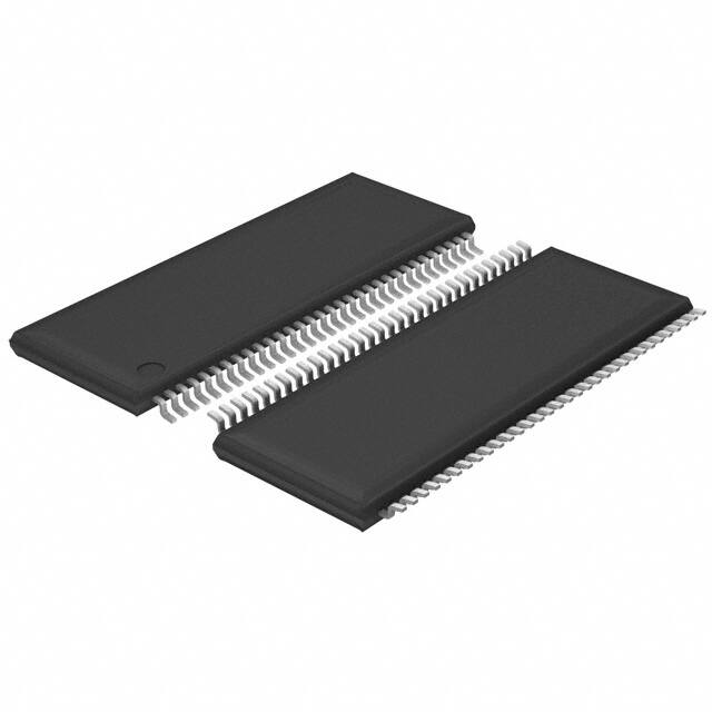
64-Pin TSSOP
* Internal Pull-Up Resistor
** Internal Pull-Down Resistor
RESET pin is 3.3V tolerant
1137–09/05/08
�ICS9LPRS511
Advance Information
Integrated
Circuit
Systems, Inc.
Pin Description
Pin# Pin Name
Type Pin Description
Asynchronous input pin used in combination with VTTPWRGD signal to determine
IN
whether to reset I2c.
PWR Ground pin.
PWR Power supply, nominal 3.3V
Latch input to select PCIEX0 and DOT96 output. GSEL = 1, selects DOT 96Mhz ;
I/O GSEL = 0, selects PCIEX0. /
24.576Mhz clock output
PWR Power supply for PCI clocks, nominal 3.3V
PWR Ground pin.
Dynamic Over Clocking pin: real time frequency selection 0: Normal; 1: Frequency will
IN
transition to a preprogrammed value in the I2c.
OUT PCI clock output.
OUT Programmable 3x strength PCICLK, default 2x
1
**RLATCH
2
3
GND
VDD
4
**GSEL/24.576Mhz
5
6
VDDPCI
GND
7
**DOC_1
8
9
PCICLK0
PCICLK1_3x
10
FSLB/PCICLK2_2x
11
SELRSET/RESET#/PCICLK3
12
PCICLK4
13
**DOC_0
14
VDD48
15
FSLA/USB_48MHz
I/O
16
*SEL24_48#/24_48Mhz
I/O
17
GND
18
Vtt_PwrGd/WOL_STOP#
IN
19
DOT96T_LR/PCIeT_LR0
OUT
20
DOT96C_LR/PCIeC_LR0
OUT
21
GND
PWR
22
PCIeT_LR1
OUT
23
PCIeC_LR1
OUT
24
PCIeT_LR2
OUT
25
PCIeC_LR2
OUT
26
GND
PWR
27
PCIeT_LR3
OUT
28
PCIeC_LR3
OUT
29
PCIeT_LR4
OUT
30
PCIeC_LR4
OUT
31
32
GND
VDDPCIEX
PWR
PWR
I/O
3.3V tolerant input for CPU frequency selection. Low voltage threshold inputs, see
input electrical characteristics for Vil_FS and Vih_FS values. / 3.3V PCI clock output.
Latch select input pin. SELRSET = 0, selects PCICLK, SELRSET = 1 selects
RESET#
OUT PCI clock output.
Dynamic Over Clocking pin: real time frequency selection 0: Normal; 1: Frequency will
IN
transition to a preprogrammed value in the I2c.
PWR Power pin for the 48MHz output.3.3V
I/O
PWR
3.3V tolerant input for CPU frequency selection. Refer to input electrical
characteristics for Vil_FS and Vih_FS values. / Fixed 48MHz USB clock output. 3.3V.
Latched select input for 24/48MHz output / 24/48MHz clock output. 1=24MHz, 0 =
48MHz.
Ground pin.
This active high 3.3V LVTTL input is a level sensitive strobe used to determine when
latch inputs are valid and are ready to be sampled / Asynchronous active low input pin
that stops all outputs except free running 25Mhz
True clock of differential pair for 96.00MHz non-spreading DOT clock/ True clock of
PCIEX0 Clock pair - selectable by GSEL; both 0.75V differential pairs are 0.75V pushpull outputs with integrated 33ohm series resistor.
Complementary clock of differential pair for 96.00MHz non-spreading DOT clock/
Complementary clock of PCIEX0 Clock pair - selectable by GSEL; both 0.75V
differential pairs are 0.75V push-pull outputs with integrated 33ohm series resistor.
Ground pin.
True clock of 0.75V differential push-pull PCI_Express pair with integrated 33ohm
series resistor
Complement clock of 0.75V differential push-pull PCI_Express pair with integrated
33ohm series resistor
True clock of 0.75V differential push-pull PCI_Express pair with integrated 33ohm
series resistor
Complement clock of 0.75V differential push-pull PCI_Express pair with integrated
33ohm series resistor
Ground pin.
Power supply for PCI Express clocks, nominal 3.3V
1137—09/05/08
2
�ICS9LPRS511
Advance Information
Integrated
Circuit
Systems, Inc.
Pin Description (Continued)
Pin# Pin Name
33
34
35
36
37
38
39
40
41
42
43
44
45
46
47
48
49
50
51
52
53
54
55
56
57
58
59
60
61
62
63
PCIeC_LR5
PCIeT_LR5
PCIeC_LR6
PCIeT_LR6
GND
PCIeC_LR7
PCIeT_LR7
PCIeC_LR8
PCIeT_LR8
VDDA
GNDA
VDDI/O
CPUC_LR1
CPUT_LR1
VDDCPU
CPUC_LR0
CPUT_LR0
GND
SCLK
SDATA
VDDREF
X2
X1
GND
REF0_2x/FSLC
GND
SATACLKC_LR
SATACLKT_LR
VDDSATA
VDD25Mhz
GND
64
25Mhz_0F_2x/Freerun*
Type Pin Description
Complement clock of 0.75V differential push-pull PCI_Express pair with integrated
OUT
33ohm series resistor
True clock of 0.75V differential push-pull PCI_Express pair with integrated 33ohm
OUT
series resistor
Complement clock of 0.75V differential push-pull PCI_Express pair with integrated
OUT
33ohm series resistor
True clock of 0.75V differential push-pull PCI_Express pair with integrated 33ohm
OUT
series resistor
PWR Ground pin.
Complement clock of 0.75V differential push-pull PCI_Express pair with integrated
OUT
33ohm series resistor
True clock of 0.75V differential push-pull PCI_Express pair with integrated 33ohm
OUT
series resistor
Complement clock of 0.75V differential push-pull PCI_Express pair with integrated
OUT
33ohm series resistor
True clock of 0.75V differential push-pull PCI_Express pair with integrated 33ohm
OUT
series resistor
PWR 3.3V power for the PLL core.
PWR Ground pin for the PLL core.
PWR Power supply for differential outputs
Complementary clock of differential pair 0.75V push-pull CPU outputs with integrated
OUT
33ohm series resistor.
True clock of differential pair 0.75V push-pull CPU outputs with integrated 33ohm
OUT
series resistor.
PWR Supply for CPU clocks, 3.3V nominal
Complementary clock of differential pair 0.75V push-pull CPU outputs with integrated
OUT
33ohm series resistor.
True clock of differential pair 0.75V push-pull CPU outputs with integrated 33ohm
OUT
series resistor.
PWR Ground pin.
IN
Clock pin of SMBus circuitry, 5V tolerant.
I/O Data pin for SMBus circuitry, 5V tolerant.
PWR Ref, XTAL power supply, nominal 3.3V
OUT Crystal output, Nominally 14.318MHz
IN
Crystal input, Nominally 14.318MHz.
PWR Ground pin.
2x strength 14.318 MHz reference clock./ 3.3V tolerant input for CPU frequency
I/O
selection. Refer to input electrical characteristics for Vil_FS and Vih_FS values.
PWR Ground pin.
Complement clock of 0.75V push-pull differential SATA pair with integrated 33ohm
OUT
series resistor.
True clock of 0.75V push-pull differential SATA pair with integrated 33ohm series
OUT
resistor.
PWR Supply for SATA clocks, 3.3V nominal
PWR Power supply for 25MHz clocks, 3.3V nominal.
PWR Ground pin.
2x strength 25MHz clock output, 3.3V (free running by default) / Latch input to select if
I/O 25Mhz_0 is freerunning or stoppable on power up default. Freerun = 1, 25Mhz_0 is
free running, Freerun = 0, 25Mhz_0 is stoppable.
1137—09/05/08
3
�ICS9LPRS511
Advance Information
Integrated
Circuit
Systems, Inc.
General Description
ICS9LPRS511 follows the Intel CK505-compliant clock specification. This clock synthesizer provides a single chip solution for
next generation P4 Intel processors and Intel chipsets. ICS9LPRS511 is driven with a 14.318MHz crystal.
Block Diagram
24.576MHz
25MHz
48MHz, USB
24_48MHz
Frequency
Dividers
Fixed PLL
DOTCLKT96/PCIEXT0
DOTCLKC96/PCIEXC0
X1
X2
XTAL
REF0
PCICLK (4:0)
SCLK
SDATA
FSLA
FSLB
FSLC
VttPwrgd/WOL_STOP#
DOC (1:0)
SEL24_48#
SELRSET
RLATCH
GSEL
Programmable
Frequency
Divider
Array
PLL
Array
CPUCLKT (1:0)
STOP
Logic
CPUCLKC (1:0)
SATACLKT
SATACLKC
Control
Logic
PCIEXT(8:1)
PCIEXC(8:1)
Reset#
1137—09/05/08
4
�ICS9LPRS511
Advance Information
Integrated
Circuit
Systems, Inc.
Table1: CPU PLL Frequency Selection Table
CPU
PCIEX
(B21b7 = 1)
MHz
266.66
MHz
100.00
1
133.33
100.00
0
200.00
100.00
1
1
166.66
100.00
1
0
0
333.33
100.00
1
0
1
100.00
100.00
0
1
1
0
400.00
100.00
0
0
1
1
1
200.00
100.00
0
1
0
0
0
266.66
100.00
0
1
0
0
1
133.33
100.00
0
1
0
1
0
200.00
100.00
0
1
0
1
1
166.66
100.00
0
1
1
0
0
333.33
100.00
0
1
1
0
1
100.00
100.00
0
1
1
1
0
400.00
100.00
0
1
1
1
1
200.00
100.00
1
0
0
0
0
269.33
101.00
1
0
0
0
1
134.66
101.00
1
0
0
1
0
202.00
101.00
1
0
0
1
1
168.33
101.00
1
0
1
0
0
274.66
103.00
1
0
1
0
1
137.33
103.00
1
0
1
1
0
206.00
103.00
1
0
1
1
1
N/A
N/A
1
1
0
0
0
279.99
105.00
1
1
0
0
1
140.00
105.00
1
1
0
1
0
210.00
105.00
1
1
0
1
1
N/A
N/A
1
1
1
0
0
285.33
107.00
1
1
1
0
1
142.66
107.00
1
1
1
1
0
214.00
107.00
1
1
1
1
1
N/A
N/A
B0b4
B0b3
B0b2
B0b1
B0b0
0
0
FSLC
0
FSLB FSLA
0
0
0
0
0
0
0
0
0
1
0
0
0
0
0
0
0
0
Spread
%
0-0.5% Down
0-0.5% Down
0-0.5% Down
0-0.5% Down
0-0.5% Down
0-0.5% Down
0-0.5% Down
0-0.5% Down
+/-0.25% Center
+/-0.25% Center
+/-0.25% Center
+/-0.25% Center
+/-0.25% Center
+/-0.25% Center
+/-0.25% Center
+/-0.25% Center
+/- 0.3% Center
+/- 0.3% Center
+/- 0.3% Center
+/- 0.3% Center
+/- 0.3% Center
+/- 0.3% Center
+/- 0.3% Center
+/- 0.3% Center
+/- 0.3% Center
+/- 0.3% Center
+/- 0.3% Center
+/- 0.3% Center
+/- 0.3% Center
+/- 0.3% Center
+/- 0.3% Center
+/- 0.3% Center
1137—09/05/08
5
�ICS9LPRS511
Advance Information
Integrated
Circuit
Systems, Inc.
Table2: PCIEX PLL Frequency Selection Table
B19b4 B19b3 B19b2 B19b1 B19b0
PCIEX
(B21b7 = 0)
PCI
SATA (B21b6 = 0)
0
0
FSLC
0
FSLB
0
FSLA
0
MHz
100.00
MHz
33.33
MHz
100.00
0
0
0
0
1
100.00
33.33
100.00
0
0
0
1
0
100.00
33.33
100.00
0
0
0
1
1
100.00
33.33
100.00
0
0
1
0
0
100.00
33.33
100.00
0
0
1
0
1
100.00
33.33
100.00
0
0
1
1
0
100.00
33.33
100.00
0
0
1
1
1
100.00
33.33
100.00
0
1
0
0
0
100.00
33.33
100.00
0
1
0
0
1
100.00
33.33
100.00
0
1
0
1
0
100.00
33.33
100.00
0
1
0
1
1
100.00
33.33
100.00
0
1
1
0
0
100.00
33.33
100.00
0
1
1
0
1
100.00
33.33
100.00
0
1
1
1
0
100.00
33.33
100.00
0
1
1
1
1
100.00
33.33
100.00
1
0
0
0
0
101.00
33.66
101.00
1
0
0
0
1
101.00
33.66
101.00
1
0
0
1
0
101.00
33.66
101.00
1
0
0
1
1
101.00
33.66
101.00
1
0
1
0
0
103.00
34.33
103.00
1
0
1
0
1
103.00
34.33
103.00
1
0
1
1
0
103.00
34.33
103.00
1
0
1
1
1
103.00
34.33
103.00
1
1
0
0
0
105.00
35.00
105.00
1
1
0
0
1
105.00
35.00
105.00
1
1
0
1
0
105.00
35.00
105.00
1
1
0
1
1
105.00
35.00
105.00
1
1
1
0
0
107.00
35.66
107.00
1
1
1
0
1
107.00
35.66
107.00
1
1
1
1
0
107.00
35.66
107.00
1
1
1
1
1
107.00
35.66
107.00
1137—09/05/08
6
Spread
%
0-0.5% Down
0-0.5% Down
0-0.5% Down
0-0.5% Down
0-0.5% Down
0-0.5% Down
0-0.5% Down
0-0.5% Down
+/-0.25% Center
+/-0.25% Center
+/-0.25% Center
+/-0.25% Center
+/-0.25% Center
+/-0.25% Center
+/-0.25% Center
+/-0.25% Center
+/- 0.3% Center
+/- 0.3% Center
+/- 0.3% Center
+/- 0.3% Center
+/- 0.3% Center
+/- 0.3% Center
+/- 0.3% Center
+/- 0.3% Center
+/- 0.3% Center
+/- 0.3% Center
+/- 0.3% Center
+/- 0.3% Center
+/- 0.3% Center
+/- 0.3% Center
+/- 0.3% Center
+/- 0.3% Center
�ICS9LPRS511
Advance Information
Integrated
Circuit
Systems, Inc.
General I2C serial interface information for the ICS9LPRS511
How to Write:
How to Read:
Controller (host) sends a start bit.
Controller (host) sends the write address D2 (H)
ICS clock will acknowledge
Controller (host) sends the beginning byte location = N
ICS clock will acknowledge
Controller (host) sends the data byte count = X
ICS clock will acknowledge
Controller (host) starts sending Byte N through
Byte N + X -1
(see Note 2)
• ICS clock will acknowledge each byte one at a time
• Controller (host) sends a Stop bit
•
•
•
•
•
•
•
•
•
•
•
•
•
•
•
•
•
•
•
•
•
•
Controller (host) will send start bit.
Controller (host) sends the write address D2 (H)
ICS clock will acknowledge
Controller (host) sends the begining byte
location = N
ICS clock will acknowledge
Controller (host) will send a separate start bit.
Controller (host) sends the read address D3 (H)
ICS clock will acknowledge
ICS clock will send the data byte count = X
ICS clock sends Byte N + X -1
ICS clock sends Byte 0 through byte X (if X(H)
was written to byte 8).
Controller (host) will need to acknowledge each byte
Controller (host) will send a not acknowledge bit
Controller (host) will send a stop bit
Index Block Read Operation
Index Block Write Operation
Controller (Host)
starT bit
T
Slave Address D2(H)
WR
WRite
Controller (Host)
T
starT bit
Slave Address D2(H)
WR
WRite
ICS (Slave/Receiver)
ICS (Slave/Receiver)
ACK
ACK
Beginning Byte = N
Beginning Byte = N
ACK
ACK
RT
Repeat starT
Slave Address D3(H)
RD
ReaD
Data Byte Count = X
ACK
Beginning Byte N
ACK
X Byte
ACK
Data Byte Count = X
ACK
Beginning Byte N
Byte N + X - 1
ACK
X Byte
ACK
P
stoP bit
Byte N + X - 1
N
P
1137—09/05/08
7
Not acknowledge
stoP bit
�ICS9LPRS511
Advance Information
Integrated
Circuit
Systems, Inc.
I2C Table: Frequency Select Register
Byte 0
Name
Control Function
Type
0
1
PWD
A/B
PWD
C/D/E/H/J
Bit 7
ROD
Reset on Demand
RW
Disable
Enable
0
0
ON
1
0
ON
1
0
0
Latch
Latch
Latch
1
0
0
Latch
Latch
Latch
Bit 6
PCIEX_SS
PCIEX PLL Spread Enable
RW
OFF
Bit 5
Bit 4
Bit 3
Bit 2
Bit 1
Bit 0
CPU_SS
FS4
FS3
FSLC
FSLB
FSLA
CPU PLL Spread Enable
Freq Select Bit 4
Freq Select Bit 3
Freq Select Bit 2
Freq Select Bit 1
Freq Select Bit 0
RW
RW
RW
RW
RW
RW
OFF
See Table 1: Frequency Selection Table
I2C Table: Frequency Select Register
Byte 1
Name
Control Function
Type
0
1
Bit 7
Bit 6
Bit 5
Bit 4
Bit 3
SEL24_48
I2c RB
SELRSET
PCIEX PLL MNEN
CPU PLL MNEN
RW
RW
RW
RW
RW
48
Shadow RAM
PCICLK4
Disable
Disable
24
Active RAM
Reset#
Enable
Enable
Bit 2
25Mhz_0F
RW
Stoppable
Free-running
latch
Bit 1
Bit 0
Reserved
GSEL
Select 24_48Mhz
Select I2c readback from
Select RESET
PCIEX PLL M/N Enable
CPU PLL M/N Enable
Free-running control
during WOL_STOP
Reserved
GSEL selection
PWD
A/B/C/D/E/H/J
latch
1
latch
0
0
RW
RW
PCIEX0
DOT96Mhz
0
latch
I2C Table: Output Control Register
Byte 2
Name
Control Function
Type
0
1
Bit 7
Bit 6
Bit 5
Bit 4
Bit 3
Bit 2
Bit 1
Bit 0
USB_48Mhz
PCIEXT/C8
SATACLK
PCICLK5
PCICLK4
PCICLK3
PCICLK2
Reserved
Output Control
Output Control
Output Control
Output Control
Output Control
Output Control
Output Control
Reserved
RW
RW
RW
RW
RW
RW
RW
RW
Disable
Disable
Disable
Disable
Disable
Disable
Disable
-
Enable
Enable
Enable
Enable
Enable
Enable
Enable
-
PWD
A/B/C/D/E/H/J
1
1
1
1
1
1
1
1
I2C Table: Output Control Register
Byte 3
Name
Control Function
Type
0
1
Bit 7
Bit 6
Bit 5
Bit 4
Bit 3
Bit 2
Bit 1
Bit 0
PCICLK1
PCICLK0
PCIEXT/C7
PCIEXT/C6
PCIEXT/C5
PCIEXT/C4
PCIEXT/C3
Output Control
Output Control
Output Control
Output Control
Output Control
Output Control
Output Control
RW
RW
RW
RW
RW
RW
RW
PCIEXT/C2
Output Control
RW
Disable
Disable
Disable
Disable
Disable
Disable
Disable
Disable
Enable
Enable
Enable
Enable
Enable
Enable
Enable
Enable
0
1
PWD
A/B/C/D/E/H/J
1
1
1
1
1
1
1
1
I2C Table: Output Control Register
Byte 4
Name
Control Function
Bit 7
Bit 6
Bit 5
Bit 4
Bit 3
PCIEXT/C1
REF0
CPUCLK1
CPUCLK0
24.576Mhz
Output Control
Output Control
Output Control
Output Control
Output Control
RW
RW
RW
RW
RW
Disable
Disable
Disable
Disable
Disable
Enable
Enable
Enable
Enable
Enable
PWD
A/B/C/D/E/H/J
1
1
1
1
1
Bit 2
Dot96Mhz/PCIEXT/C0
Output Control
RW
Disable
Enable
1
Bit 1
Bit 0
25Mhz_0F
Reserved
Output Control
Reserved
RW
RW
Disable
-
Enable
-
1
1
1137—09/05/08
8
�ICS9LPRS511
Advance Information
Integrated
Circuit
Systems, Inc.
I2C Table: Output Control Register
Byte 5
Bit
Bit
Bit
Bit
7
6
5
4
Bit 3
Bit 2
Bit 1
Bit 0
0
1
RW
RW
RW
RW
Disable
00 = 600mV
10 = 800mV
-
Enable
01 = 900mV
11 = 700mV
-
PWD
A/B/C/D/E/H/J
1
1
0
0
iAMT Enable Control
RW
Stoppable
Free-running
0
Reserved
Reserved
IIC Load control
RW
RW
RW
Load
Do not Load
0
0
0
Name
Control Function
Type
0
1
Reserved
Reserved
Reserved
Reserved
Reserved
Reserved
Reserved
Reserved
Reserved
Reserved
Reserved
Reserved
Reserved
Reserved
Reserved
Reserved
RW
RW
RW
RW
RW
RW
RW
RW
-
-
Name
Control Function
24_48Mhz
Diff AMP
Diff AMP
Reserved
iAMT EN (only
applicable to revisions
H and J, otherwise
this is a reserved bit)
Reserved
Reserved
Load Control
Output Control
Differential output
Amplitude Control
Reserved
I2C Table: Reserved Register
Byte 6
Bit
Bit
Bit
Bit
Bit
Bit
Bit
Bit
7
6
5
4
3
2
1
0
PWD
A/B/C/D/E/H/J
0
0
0
0
0
0
0
0
I2C Table: Revision and Vendor ID Register
Byte 7
Bit
Bit
Bit
Bit
Bit
Bit
Bit
Bit
Name
Control Function
RID3
RID2
RID1
RID0
VID3
VID2
VID1
VID0
7
6
5
4
3
2
1
0
Type
0
1
R
R
R
R
R
R
R
R
001 = ICS
-
-
Revision ID
VENDOR ID
PWD
A/B
0
0
0
0
0
0
0
1
PWD
C/D
0
0
1
0
0
0
0
1
I2C Table: Byte Count Register
Byte 8
Bit
Bit
Bit
Bit
Bit
Bit
Bit
Bit
Name
BC7
BC6
BC5
BC4
BC3
BC2
BC1
BC0
7
6
5
4
3
2
1
0
PWD
A/B/C/D/E/H/J
0
0
0
Writing to this register will configure how many bytes will be
0
read back, default is 0F = 15 bytes.
1
1
1
1
0
1
Type
0
1
PWD
A/B/C/D/E/H/J
RW
Disable
Enable
0
RW
Disable
Enable
0
R
R
Normal
Normal
Alarm
Alarm
X
X
RW
290ms Base
1160ms Base
0
Control Function
Type
Byte Count Programming
b(7:0)
R
R
R
RW
RW
RW
RW
RW
I2C Table: Watch Dog Timer Control Register
Byte 9
Name
Bit 7
HWD_EN
Bit 6
SWD_EN
Bit 5
Bit 4
WD Hard Status
WD Soft Status
Bit 3
WDTCtrl
Bit 2
HWD2
Control Function
Watchdog Hard Alarm
Enable
Watchdog Soft Alarm
Enable
WD Hard Alarm Status
WD Soft Alarm Status
Watch Dog Alarm Time
base Control
WD Hard Alarm Timer Bit 2
RW
Bit 1
HWD1
WD Hard Alarm Timer Bit 1
RW
Bit 0
HWD0
WD Hard Alarm Timer Bit 0
RW
1
These bits represent X*290ms (or 1.16S) the watchdog timer
waits before it goes to alarm mode. Default is 7 X 290ms =
2s.
1
1
1137—09/05/08
9
PWD PWD PWD
E
H
J
0
0
0
1
1
1
0
0
1
0
1
0
0
0
0
0
0
0
0
0
0
1
1
1
�ICS9LPRS511
Advance Information
Integrated
Circuit
Systems, Inc.
I2C Table: WD Safe Frequency Control Register
Byte 10
Name
Control Function
Type
Bit 7
Bit 6
Bit 5
Bit 4
Bit 3
Bit 2
Bit 1
Bit 0
SWD2
SWD1
SWD0
WD SF4
WD SF3
WD SF2
WD SF1
WD SF0
WD Soft Alarm Timer Bit 2
WD Soft Alarm Timer Bit 1
WD Soft Alarm Timer Bit 0
RW
RW
RW
RW
RW
RW
RW
RW
Watch Dog Safe Freq
Programming bits
PWD
A/B/C/D/E/H/J
1
These bits represent X*290ms (or 1.16S) the watchdog timer
waits before it goes to alarm mode. Default is 7 X 290ms =
1
2s.
1
0
0
Writing to these bit will configure the safe frequency as
0
Byte10 bit (4:0).
0
0
0
1
I2C Table: CPU PLL Frequency Control Register
Byte 11
Name
Control Function
Type
Bit 7
Bit 6
Bit 5
Bit 4
Bit 3
Bit 2
Bit 1
Bit 0
N Div2
N Div1
M Div5
M Div4
M Div3
M Div2
M Div1
M Div0
N Divider Prog bit 2
N Divider Prog bit 1
RW
RW
RW
RW
RW
RW
RW
RW
M Divider Programming
bit (5:0)
PWD
A/B/C/D/E/H/J
X
X
X
The decimal representation of M and N Divider in Byte 11
X
and 12 will configure the CPU PLL VCO frequency. Default
at power up = latch-in or Byte 0 Rom table. VCO Frequency
X
= 14.318 x Ndiv(10:0)/Mdiv(5:0)
X
X
X
0
1
I2C Table: CPU PLL Frequency Control Register (DOC0 = 0)
Byte 12
Name
Bit 7
Bit 6
Bit 5
Bit 4
Bit 3
Bit 2
Bit 1
Bit 0
N Div10
N Div9
N Div8
N Div7
N Div6
N Div5
N Div4
N Div3
Control Function
Type
N Divider Programming
Byte12 bit(7:0) and Byte11
bit(7:6)
RW
RW
RW
RW
RW
RW
RW
RW
PWD
A/B/C/D/E/H/J
X
X
X
The decimal representation of M and N Divider in Byte 11
X
and 12 will configure the CPU PLL VCO frequency. Default
at power up = latch-in or Byte 0 Rom table. VCO Frequency
X
= 14.318 x Ndiv(10:0)/Mdiv(5:0)
X
X
X
0
1
I2C Table: CPU PLL Spread Spectrum Control Register
Byte 13
Name
Bit 7
Bit 6
Bit 5
Bit 4
Bit 3
Bit 2
Bit 1
Bit 0
SSP7
SSP6
SSP5
SSP4
SSP3
SSP2
SSP1
SSP0
Control Function
Type
Spread Spectrum
Programming bit(7:0)
RW
RW
RW
RW
RW
RW
RW
RW
PWD
A/B/C/D/E/H/J
X
X
X
X
These Spread Spectrum bits in Byte 13 and 14 will program
the spread percentage of CPU PLL
X
X
X
X
0
1
I2C Table: CPU PLL Spread Spectrum Control Register
Byte 14
Name
Bit 7
Bit 6
Bit 5
Bit 4
Bit 3
Bit 2
Bit 1
Bit 0
SSP15
SSP14
SSP13
SSP12
SSP11
SSP10
SSP9
SSP8
Control Function
Type
Spread Spectrum
Programming bit(14:8)
RW
RW
RW
RW
RW
RW
RW
RW
PWD
A/B/C/D/E/H/J
0
X
X
These Spread Spectrum bits in Byte 13 and 14 will program
X
the spread percentage of CPU PLL
X
X
X
X
0
1137—09/05/08
10
1
�ICS9LPRS511
Advance Information
Integrated
Circuit
Systems, Inc.
I2C Table: PCIEX PLL Frequency Control Register
Byte 15
Name
Control Function
Type
Bit 7
Bit 6
Bit 5
Bit 4
Bit 3
Bit 2
Bit 1
Bit 0
N Div2
N Div1
M Div5
M Div4
M Div3
M Div2
M Div1
M Div0
N Divider Prog bit 2
N Divider Prog bit 1
RW
RW
RW
RW
RW
RW
RW
RW
M Divider Programming
bit (5:0)
PWD
A/B/C/D/E/H/J
X
X
X
The decimal representation of M and N Divider in Byte 15
and 16 will configure the PCIEX PLL VCO frequency. Default
X
at power up = latch-in or Byte 0 Rom table. VCO Frequency
X
= 14.318 x Ndiv(10:0)/Mdiv(5:0)
X
X
X
0
1
I2C Table: PCIEX PLL Frequency Control Register (DOC0 = 0)
Byte 16
Name
Bit 7
Bit 6
Bit 5
Bit 4
Bit 3
Bit 2
Bit 1
Bit 0
N Div10
N Div9
N Div8
N Div7
N Div6
N Div5
N Div4
N Div3
Control Function
Type
N Divider Programming
Byte16 bit(7:0) and Byte15
bit(7:6)
RW
RW
RW
RW
RW
RW
RW
RW
PWD
A/B/C/D/E/H/J
X
X
X
The decimal representation of M and N Divider in Byte 15
and 16 will configure the PCIEX PLL VCO frequency. Default
X
at power up = latch-in or Byte 0 Rom table. VCO Frequency
X
= 14.318 x Ndiv(10:0)/Mdiv(5:0)
X
X
X
0
1
I2C Table: PCIEX PLL Spread Spectrum Control Register
Byte 17
Name
Bit 7
Bit 6
Bit 5
Bit 4
Bit 3
Bit 2
Bit 1
Bit 0
SSP7
SSP6
SSP5
SSP4
SSP3
SSP2
SSP1
SSP0
Control Function
Type
Spread Spectrum
Programming bit(7:0)
RW
RW
RW
RW
RW
RW
RW
RW
PWD
A/B/C/D/E/H/J
X
X
X
These Spread Spectrum bits in Byte 17 and 18 will program
X
the spread percentage of PCIEX PLL
X
X
X
X
0
1
I2C Table: PCIEX PLL Spread Spectrum Control Register
Byte 18
Name
Bit 7
Bit 6
Bit 5
Bit 4
Bit 3
Bit 2
Bit 1
Bit 0
SSP15
SSP14
SSP13
SSP12
SSP11
SSP10
SSP9
SSP8
Control Function
Type
Spread Spectrum
Programming bit(14:8)
RW
RW
RW
RW
RW
RW
RW
RW
PWD
A/B/C/D/E/H/J
0
X
X
X
These Spread Spectrum bits in Byte 17 and 18 will program
the spread percentage of PCIEX PLL
X
X
X
X
0
1
I2C Table: PCIEX PLL Frequency Select Register
Byte 19
Name
Control Function
Type
0
1
Bit 7
Bit 6
Bit 5
Bit 4
Bit 3
Bit 2
Bit 1
Bit 0
Reserved
Reserved
Reserved
FS4
FS3
FSLC
FSLB
FSLA
Reserved
Reserved
Reserved
Freq Select Bit 4
Freq Select Bit 3
Freq Select Bit 2
Freq Select Bit 1
Freq Select Bit 0
RW
RW
RW
RW
RW
RW
RW
RW
-
-
See Table 2: PCIEX PLL Frequency Selection Table
1137—09/05/08
11
PWD
A/B/C/D/E/H/J
1
0
0
0
0
Latch
Latch
Latch
�ICS9LPRS511
Advance Information
Integrated
Circuit
Systems, Inc.
I2C Table: Output Control Register
Byte 20
Bit
Bit
Bit
Bit
Bit
Bit
Bit
7
6
5
4
3
2
1
Bit 0
Name
Control Function
Type
0
1
Reserved
Reserved
Reserved
Reserved
PCIEX PLL TBEN
CPU PLL TBEN
Reserved
Reserved
Reserved
Reserved
Reserved
PCIEX PLL Turbo Enable
CPU PLL Turbo Enable
Reserved
Reset Synchronization
upon Reset (Byte 21)
RW
RW
RW
RW
RW
RW
RW
Disable
Disable
-
Enable
Enable
-
PWD
A/B/C/D/E/H/J
0
0
0
0
0
0
0
RW
Disable
Enable
0
RESET Sync
I2C Table: Synchronization Control Register
PWD
A/B
0
1
1
1
1
1
1
1
Byte 21
Name
Control Function
Type
0
1
Bit 7
Bit 6
Bit 5
Bit 4
Bit 3
Bit 2
Bit 1
Bit 0
PCIEX Source
SATA Source
Reserved
Reserved
Reserved
Reserved
Reserved
Reserved
PCIEX Source
SATA Source
Reserved
Reserved
Reserved
Reserved
Reserved
Reserved
RW
RW
RW
RW
RW
RW
RW
RW
PCIEX PLL
PCIEX PLL
-
CPU PLL
Fixed PLL
-
Control Function
Type
0
1
PWD
A/B/C/D/E/H/J
RW
Enabled
Disabled
1
RW
Enabled
Disabled
0
RW
RW
RW
RW
RW
RW
-
-
0
0
0
0
1
1
0
1
I2C Table: DOC pin control register
Byte 22
Name
Bit 7
PCIEX
Bit 6
CPU
Bit 5
Bit 4
Bit 3
Bit 2
Bit 1
Bit 0
Reserved
Reserved
Reserved
Reserved
Reserved
Reserved
PCIEX PLL DOC0 pin
control
CPU PLL DOC0 pin
control
Reserved
Reserved
Reserved
Reserved
Reserved
Reserved
I2C Table: CPU PLL DOC 1 N programming Register (DOC0 = 1)
Byte 23
Name
Bit 7
Bit 6
Bit 5
Bit 4
Bit 3
Bit 2
Bit 1
Bit 0
N Div10
N Div9
N Div8
N Div7
N Div6
N Div5
N Div4
N Div3
Control Function
Type
N Divider Programming
Byte23 bit(7:0) and Byte11
bit(7:6)
RW
RW
RW
RW
RW
RW
RW
RW
The decimal representation of M and N Divider in Byte 11
and 23 will configure the CPU PLL VCO frequency. VCO
Frequency = 14.318 x Ndiv(10:0)/Mdiv(5:0)
PWD
A/B/C/D/E/H/J
X
X
X
X
X
X
X
X
Bytes 24 and 25 are reserved
I2C Table: PCIEX PLL DOC 1 N programming Register (DOC0 = 1)
Byte 26
Name
Bit 7
Bit 6
Bit 5
Bit 4
Bit 3
Bit 2
Bit 1
Bit 0
N Div10
N Div9
N Div8
N Div7
N Div6
N Div5
N Div4
N Div3
Control Function
Type
N Divider Programming
Byte26 bit(7:0) and Byte15
bit(7:6)
RW
RW
RW
RW
RW
RW
RW
RW
0
1
The decimal representation of M and N Divider in Byte 15
and 26 will configure the PCIEX PLL VCO frequency. VCO
Frequency = 14.318 x Ndiv(10:0)/Mdiv(5:0)
1137—09/05/08
12
PWD
A/B/C/D/E/H/J
X
X
X
X
X
X
X
X
PWD
C/D/E/H
1
1
1
1
1
1
1
1
PWD
J
0
1
1
1
1
1
1
1
�ICS9LPRS511
Advance Information
Integrated
Circuit
Systems, Inc.
Bytes 27 and 28 are reserved
I2C Table: Programmable output divider Register
Byte 29
Bit
Bit
Bit
Bit
Bit
Bit
Bit
Bit
7
6
5
4
3
2
1
0
Name
CPUDiv3
CPUDiv2
CPUDiv1
CPUDiv0
PCIEXDiv3
PCIEXDiv2
PCIEXDiv1
PCIEXDiv0
Control Function
CPU Divider Ratio
Programming Bits
PCIEX Divider Ratio
Programming Bits for CPU
PLL
0
Type
RW
RW
RW
RW
RW
RW
RW
RW
0000:/2
0001:/3
0010:/5
0011:/7
0000:/2
0001:/3
0010:/5
0011:/7
1100:/16
1101:/24
1110:/20
1111:/56
1100:/10
1101:/24
1110:/20
1111:/56
PWD
A/B/C/D/E/H/J
X
X
X
X
X
X
X
X
1100:/40
1101:/24
1110:/N/A
1111:/N/A
1100:/N/A
1101:/24
1110:/72
1111:/N/A
PWD
A/B/C/D/E/H/J
X
X
X
X
X
X
X
X
1
0100:/4
0101:/6
0110:/10
0111:/14
0100:/4
0101:/6
0110:/10
0111:/14
1000:/8
1001:/12
1010:/20
1011:/28
1000:/8
1001:/12
1010:/20
1011:/28
I2C Table: Programmable output divider Register
Byte 30
Bit
Bit
Bit
Bit
Bit
Bit
Bit
Bit
7
6
5
4
3
2
1
0
Name
PCIEXDiv3
PCIEXDiv2
PCIEXDiv1
PCIEXDiv0
PCIDiv3
PCIDiv2
PCIDiv1
PCIDiv0
Control Function
PCIEX Divider Ratio
Programming Bits for
PCIEX PLL
PCI Divider Ratio
Programming Bits
0
Type
RW
RW
RW
RW
RW
RW
RW
RW
0000:/5
0001:/3
0010:/N/A
0011:/N/A
0000:/N/A
0001:/3
0010:/9
0011:/N/A
1
0100:/10
0101:/6
0110:/N/A
0111:/N/A
0100:/N/A
0101:/6
0110:/18
0111:/N/A
1000:/20
1001:/12
1010:/N/A
1011:/N/A
1000:/N/A
1001:/12
1010:/36
1011:/N/A
I2C Table: Strength Control Register
Byte 31
Bit
Bit
Bit
Bit
Bit
Bit
Bit
Bit
7
6
5
4
3
2
1
0
Name
25Str_1
25Str_0
REFStr_1
REFStr_0
PCIStr_1
PCIStr_0
PCIStr_1
PCIStr_0
Control Function
25Mhz_0 Strength Control
REFCLK0 Strength Control
PCICLK1 Strength Control
PCICLK2 Strength Control
Type
0
1
RW
RW
RW
RW
RW
RW
RW
RW
00 = tristated
01 = 0.1x
00 = tristated
01 = 0.1x
00 = tristated
01 = 2.00x
00 = tristated
01 = 0.1x
10 = 1.00x
11 = 2.00x
10 = 1.00x
11 = 2.00x
10 = 1.00x
11 = 3.00x
10 = 1.00x
11 = 2.00x
Type
0
1
PWD
A/B/C/D/E/H/J
1
1
1
1
0
1
1
1
I2C Table: Skew programming Register
Byte 32
Bit
Bit
Bit
Bit
Bit
Bit
Bit
Bit
7
6
5
4
3
2
1
0
Name
CPUSkw3
CPUSkw2
CPUSkw1
CPUSkw0
CPUSkw3
CPUSkw2
CPUSkw1
CPUSkw0
Control Function
CPUCLK0 Skew Control
(ps)
CPUCLK1 Skew Control
(ps)
RW
RW
RW
RW
RW
RW
RW
RW
0000:0
0001:100
0010:200
0011:300
0000:0
0001:100
0010:200
0011:300
1137—09/05/08
13
0100:400
0101:500
0110:600
0111:700
0100:400
0101:500
0110:600
0111:700
1000:800
1001:900
1010:1000
1011:1100
1000:800
1001:900
1010:1000
1011:1100
1100:1200
1101:1300
1110:1400
1111:1500
1100:1200
1101:1300
1110:1400
1111:1500
PWD
A/B/C/D/E/H/J
0
0
0
0
0
0
0
0
�ICS9LPRS511
Advance Information
Integrated
Circuit
Systems, Inc.
Absolute Maximum Ratings
PARAMETER
SYMBOL
CONDITIONS
MIN
MAX
UNITS Notes
Maximum Supply Voltage
VDDxxx
Supply Voltage
4.6
V
1,7
Maximum Supply Voltage
VDDxxx_IO
Low-Voltage Differential I/O Supply
3.8
V
1,7
Maximum Input Voltage
VIH
3.3V LVCMOS Inputs
4.6
V
1,7,8
Minimum Input Voltage
VIL
Any Input
GND - 0.5
V
1,7
Storage Temperature
Ts
-
-65
150
°
C
1,7
Case Temperature
Tcase
-
115
°C
1
Input ESD protection
ESD prot
Human Body Model
V
1,7
2000
Electrical Characteristics - Input/Supply/Common Output Parameters
PARAMETER
SYMBOL
CONDITIONS
MIN
MAX
Ambient Operating Temp
Tambient
-
0
70
°C
1
Supply Voltage
VDDxxx
Supply Voltage
3.135
3.465
V
1
Supply Voltage
VDDxxx_IO
Low-Voltage Differential I/O Supply
1.05
3.465
V
1
Input High Voltage
VIHSE
Single-ended inputs
2
VDD + 0.3
V
1
Input Low Voltage
VILSE
Single-ended inputs
VSS - 0.3
0.8
V
1
Input Leakage Current
IIN
-5
5
uA
1
Input Leakage Current
IINRES
VIN = VDD , VIN = GND
Inputs with pull or pull down
resistors
VIN = VDD , VIN = GND
-200
200
uA
1
Output High Voltage
VOHSE
V
1
Single-ended outputs, IOH = -1mA
Output Low Voltage
VOLSE
Single-ended outputs, IOL = 1 mA
Output High Voltage
VOHDIF
Differential Outputs, IOH = TBD mA
Output Low Voltage
Low Threshold InputHigh Voltage (Test Mode)
Low Threshold InputHigh Voltage
Low Threshold InputLow Voltage
VOLDIF
Differential Outputs, IOL = TBD mA
VIH_FS_TEST
3.3 V +/-5%
VIH_FS
VIL_FS
Operating Supply Current
iAMT Mode Current
0.4
V
1
0.9
V
1
0.4
V
1
2
VDD + 0.3
V
1
3.3 V +/-5%
0.7
1.5
V
1
3.3 V +/-5%
VSS - 0.3
0.35
V
1
0.7
IDD_DEFAULT
3.3V supply, PLL3 off
TBD
mA
1
IDD_PLL3DIF
TBD
mA
1
TBD
mA
1
TBD
mA
1
IDD_PD3.3
3.3V supply, PLL3 Differential Out
3.3V supply, PLL3 Single-ended
Out
0.8V supply, Differential IO current,
all outputs enabled
3.3V supply, Power Down Mode
TBD
mA
1
IDD_PDIO
0.8V IO supply, Power Down Mode
TBD
mA
1
IDD_iAMT3.3
3.3V supply, iAMT Mode
TBD
mA
1
IDD_PLL3SE
IDD_IO
Power Down Current
2.4
UNITS Notes
IDD_iAMT0.8
0.8V IO supply, iAMTMode
TBD
mA
1
Input Frequency
Fi
VDD = 3.3 V
TBD
MHz
2
Pin Inductance
Lpin
7
nH
1
CIN
Logic Inputs
5
pF
1
Input Capacitance
COUT
Output pin capacitance
6
pF
1
CINX
X1 & X2 pins
TBD
pF
1
fSSMOD
Triangular Modulation
33
kHz
1
Spread Spectrum Modulation
Frequency
1137—09/05/08
14
1.5
30
�ICS9LPRS511
Advance Information
Integrated
Circuit
Systems, Inc.
AC Electrical Characteristics - Input/Common Parameters
PARAMETER
SYMBOL
Clk Stabilization
TSTAB
Tdrive_SRC
T DRSRC
Tdrive_PD#
TDRPD
Tdrive_CPU
T DRSRC
Tfall_PD#
T FALL
Trise_PD#
T RISE
CONDITIONS
From VDD Power-Up or deassertion of PD# to 1st clock
SRC output enable after
PCI_STOP# de-assertion
Differential output enable after
PD# de-assertion
CPU output enable after
CPU_STOP# de-assertion
MIN
Fall/rise time of PD#, PCI_STOP#
and CPU_STOP# inputs
MAX
UNITS Notes
1.8
ms
1
15
ns
1
300
us
1
10
ns
1
5
ns
1
5
ns
1
AC Electrical Characteristics - (CPU, PCIEX, SATACLK, DOT96Mhz)
Low Power Differential Outputs
PARAMETER
SYMBOL
CONDITIONS
MIN
MAX
Rising Edge Slew Rate
tSLR
Differential Measurement
2.5
8
UNITS NOTES
V/ns
1,2
2.5
Falling Edge Slew Rate
tFLR
Differential Measurement
8
V/ns
1,2
Slew Rate Variation
tSLVAR
Single-ended Measurement
20
%
1
Maximum Output Voltage
VHIGH
Includes overshoot
1150
mV
1
Minimum Output Voltage
VLOW
Includes undershoot
-300
mV
1
Differential Voltage Swing
VSWING
Differential Measurement
300
mV
1
300
550
mV
1,3,4
140
mV
1,3,5
55
%
1
Crossing Point Voltage
VXABS
Single-ended Measurement
Crossing Point Variation
VXABSVAR
Single-ended Measurement
Duty Cycle
DCYC
Differential Measurement
CPU Jitter - Cycle to Cycle
CPUJ C2C
Differential Measurement
85
ps
1
SRC Jitter - Cycle to Cycle
SRCJ C2C
Differential Measurement
125
ps
1
DOT Jitter - Cycle to Cycle
DOTJ C2C
Differential Measurement
250
ps
1
45
CPU[1:0] Skew
CPUSKEW10
Differential Measurement
100
ps
1
CPU[2_ITP:0] Skew
CPUSKEW20
Differential Measurement
150
ps
1
SRC[10:0] Skew
SRCSKEW
Differential Measurement
TBD
ps
1
1137—09/05/08
15
�ICS9LPRS511
Advance Information
Integrated
Circuit
Systems, Inc.
Electrical Characteristics - PCICLK/PCICLK_F
PARAMETER
SYMBOL
CONDITIONS
MIN
Long Accuracy
ppm
see Tperiod min-max values
-300
33.33MHz output nominal
Clock period
Tperiod
Absolute min/max period
Tabs
33.33MHz output nominal/spread
29.49100
Output High Voltage
VOH
IOH = -1 mA
2.4
Output Low Voltage
VOL
IOL = 1 mA
Output High Current
IOH
33.33MHz output spread
V OH @MIN = 1.0 V
29.99100
300
UNITS NOTES
1,6
ppm
6
30.00900
ns
30.15980
ns
6
ns
6
V
1
30.65980
0.4
-33
VOH@MAX = 3.135 V
VOL @ MIN = 1.95 V
MAX
-33
30
V
1
mA
1
mA
1
mA
1
Output Low Current
IOL
38
mA
1
Rising Edge Slew Rate
tSLR
Measured from 0.8 to 2.0 V
1
4
V/ns
1
Falling Edge Slew Rate
tFLR
Measured from 2.0 to 0.8 V
1
4
V/ns
1
Duty Cycle
dt1
VT = 1.5 V
45
55
%
1
Skew
tskew
VT = 1.5 V
250
ps
1
Jitter, Cycle to cycle
tjcyc-cyc
VT = 1.5 V
500
ps
1
VOL @ MAX = 0.4 V
Electrical Characteristics - USB48MHz, 24_48Mhz
PARAMETER
Long Accuracy
SYMBOL
ppm
CONDITIONS
see Tperiod min-max values
MIN
-100
MAX
100
UNITS NOTES
ppm
1,2
Clock period
Tperiod
48.00MHz output nominal
20.83125
20.83542
ns
2
Absolute min/max period
Tabs
48.00MHz output nominal
20.48130
21.18540
ns
2
Output High Voltage
VOH
IOH = -1 mA
2.4
V
1
Output Low Voltage
VOL
IOL = 1 mA
V
1
Output High Current
IOH
Output Low Current
IOL
27
mA
1
Rising Edge Slew Rate
tSLR
Measured from 0.8 to 2.0 V
1
2
V/ns
1
Falling Edge Slew Rate
tFLR
Measured from 2.0 to 0.8 V
1
2
V/ns
1
Duty Cycle
dt1
VT = 1.5 V
45
55
%
1
Jitter, Cycle to cycle
tjcyc-cyc
VT = 1.5 V
350
ps
1
V OH @MIN = 1.0 V
0.4
-29
VOH@MAX = 3.135 V
VOL @ MIN = 1.95 V
-23
29
VOL @ MAX = 0.4 V
mA
1
mA
1
mA
1
Electrical Characteristics - SMBus Interface
PARAMETER
SYMBOL
SMBus Voltage
VDD
CONDITIONS
Low-level Output Voltage
Current sinking at
VOLSMB = 0.4 V
SCLK/SDATA
Clock/Data Rise Time
SCLK/SDATA
Clock/Data Fall Time
Maximum SMBus Operating
Frequency
VOLSMB
@ IPULLUP
IPULLUP
SMB Data Pin
T FI2C
(Max VIL - 0.15) to
(Min VIH + 0.15)
(Min VIH + 0.15) to
(Max VIL - 0.15)
F SMBUS
Block Mode
T RI2C
1137—09/05/08
16
MIN
MAX
2.7
5.5
V
1
0.4
V
1
mA
1
1000
ns
1
300
ns
1
100
kHz
1
4
UNITS Notes
�ICS9LPRS511
Advance Information
Integrated
Circuit
Systems, Inc.
Electrical Characteristics - REF-14.318MHz
PARAMETER
SYMBOL
CONDITIONS
MIN
MAX
Long Accuracy
ppm
see Tperiod min-max values
-300
300
UNITS Notes
ppm
1,2
Clock period
Tperiod
14.318MHz output nominal
69.8203
69.8622
ns
2
Absolute min/max period
Tabs
14.318MHz output nominal
69.8203
70.86224
ns
2
Output High Voltage
VOH
IOH = -1 mA
2.4
V
1
Output Low Voltage
VOL
0.4
V
1
-33
-33
mA
1
30
38
mA
1
1
4
V/ns
1
IOL = 1 mA
VOH @MIN = 1.0 V,
Output High Current
IOH
Output Low Current
IOL
Rising Edge Slew Rate
tSLR
Measured from 0.8 to 2.0 V
Falling Edge Slew Rate
tFLR
Measured from 2.0 to 0.8 V
1
4
V/ns
1
Duty Cycle
dt1
VT = 1.5 V
45
55
%
1
Jitter
tjcyc-cyc
VT = 1.5 V
1000
ps
1
VOH@MAX = 3.135 V
VOL @MIN = 1.95 V,
VOL @MAX = 0.4 V
Notes on Electrical Characteristics:
1
Guaranteed by design and characterization, not 100% tested in production.
2
Slew rate measured through Vswing centered around differential zero
3
Vxabs is defined as the voltage where CLK = CLK#
4
Only applies to the differential rising edge (CLK rising and CLK# falling)
Defined as the total variation of all crossing voltages of CLK rising and CLK# falling. Matching applies to rising edge rate of
CLK and falling edge of CLK#. It is measured using a +/-75mV window centered on the average cross point where CLK meets
CLK#. The average cross point is used to calculate the voltage thresholds the oscilloscope is to use for the edge rate
calculations.
6
All Long Term Accuracy and Clock Period specifications are guaranteed assuming that REFOUT is at 14.31818MHz
5
7
Operation under these conditions is neither implied, nor guaranteed.
8
Maximum input voltage is not to exceed maximum VDD
1137—09/05/08
17
�ICS9LPRS511
Advance Information
Integrated
Circuit
Systems, Inc.
c
N
SYMBOL
L
E1
A
A1
A2
b
c
D
E
E1
e
L
N
α
aaa
E
INDEX
AREA
1 2
�
D
A
A2
6.10 mm. Body, 0.50 mm. Pitch TSSOP
(240 mil)
(20 mil)
In Millimeters
In Inches
COMMON DIMENSIONS
COMMON DIMENSIONS
MIN
MAX
MIN
MAX
-1.20
-.047
0.05
0.15
.002
.006
0.80
1.05
.032
.041
0.17
0.27
.007
.011
0.09
0.20
.0035
.008
SEE VARIATIONS
SEE VARIATIONS
8.10 BASIC
0.319 BASIC
6.00
6.20
.236
.244
0.50 BASIC
0.020 BASIC
0.45
0.75
.018
.030
SEE VARIATIONS
SEE VARIATIONS
0°
8°
0°
8°
-0.10
-.004
VARIATIONS
A1
N
-Ce
64
SEATING
PLANE
b
D mm.
MIN
16.90
D (inch)
MAX
17.10
Reference Doc.: JEDEC Publication 95, MO-153
aaa C
10-0039
Ordering Information
ICS9LPRS511yGLF-T
Example:
ICS XXXX y G LF- T
Designation for tape and reel packaging
RoHS Compliant (Optional)
Package Type
G = TSSOP
Revision Designator (will not correlate with datasheet revision)
Device Type
Prefix
ICS = Standard Device
1137—09/05/08
18
MIN
.665
MAX
.673
�ICS9LPRS511
Advance Information
Integrated
Circuit
Systems, Inc.
Revision History
Rev.
0.1
0.2
0.3
0.4
Issue Date
8/3/2005
8/17/2005
8/25/2005
8/31/2005
0.5
9/19/2005
0.6
0.7
10/6/2005
4/7/2006
0.5
0.6
7/31/2006
9/26/2006
0.7
0.8
0.9
11/2/2006
10/4/2007
9/5/2008
Description
Page #
Initial Release
Updated pinout and invert VTTPWRGD/WOL_STOP polarity
1-4
Added I2c Tables
8-21
Updated pinout (DOC1 removed, PCICLK1 added)
1-3, 19-21
1) Updated pinout, pin description (move freerun latch from
PCICLK to 25Mhz_0)
1-3, 8-18
2) Updated I2c Bytes 1, 5, 22, 31
1) Changed pin 42, 53, 61 and 62 from Standby (Non
Collapsible) Power to Standard Power.
1,3,
2) Removed Power Groups Table.
4
Updated I2C.
8-18
1. Updated Pinout.
2. Updated Pin Description.
1,2
1. Updated I2C.
8-13
1. Updated Output Features to represent low power.
2. Updated I2C.
Various
Updated Functionality and CPU frequency table
1, 5
Added Case Temperature @ 115C to Max Rating Table.
14
Silicon Revision History
Rev.
0.1
0.2
0.3
Description
B0b6 = 1 in revisions [A:B]
B0b6 = 0 in revisions [C:J]
B7 = 01h in revisions [A:B]
B7 = 21h in revisions [C:D]
B7 = 41h in revision E
B7 = 51h in revision H
B7 = 61h in revision J
B21b7 = 0 in revisions [A:B]
B21b7 = 1 in revisions [C:H]
B21b7 = 0 in revision J
1137—09/05/08
This product is protected by United States Patent NO. 7,342,420 and other patents.
19
�IMPORTANT NOTICE AND DISCLAIMER
RENESAS ELECTRONICS CORPORATION AND ITS SUBSIDIARIES (“RENESAS”) PROVIDES TECHNICAL
SPECIFICATIONS AND RELIABILITY DATA (INCLUDING DATASHEETS), DESIGN RESOURCES (INCLUDING
REFERENCE DESIGNS), APPLICATION OR OTHER DESIGN ADVICE, WEB TOOLS, SAFETY INFORMATION, AND
OTHER RESOURCES “AS IS” AND WITH ALL FAULTS, AND DISCLAIMS ALL WARRANTIES, EXPRESS OR IMPLIED,
INCLUDING, WITHOUT LIMITATION, ANY IMPLIED WARRANTIES OF MERCHANTABILITY, FITNESS FOR A
PARTICULAR PURPOSE, OR NON-INFRINGEMENT OF THIRD PARTY INTELLECTUAL PROPERTY RIGHTS.
These resources are intended for developers skilled in the art designing with Renesas products. You are solely responsible
for (1) selecting the appropriate products for your application, (2) designing, validating, and testing your application, and (3)
ensuring your application meets applicable standards, and any other safety, security, or other requirements. These
resources are subject to change without notice. Renesas grants you permission to use these resources only for
development of an application that uses Renesas products. Other reproduction or use of these resources is strictly
prohibited. No license is granted to any other Renesas intellectual property or to any third party intellectual property.
Renesas disclaims responsibility for, and you will fully indemnify Renesas and its representatives against, any claims,
damages, costs, losses, or liabilities arising out of your use of these resources. Renesas' products are provided only subject
to Renesas' Terms and Conditions of Sale or other applicable terms agreed to in writing. No use of any Renesas resources
expands or otherwise alters any applicable warranties or warranty disclaimers for these products.
(Rev.1.0 Mar 2020)
Corporate Headquarters
Contact Information
TOYOSU FORESIA, 3-2-24 Toyosu,
Koto-ku, Tokyo 135-0061, Japan
www.renesas.com
For further information on a product, technology, the most
up-to-date version of a document, or your nearest sales
office, please visit:
www.renesas.com/contact/
Trademarks
Renesas and the Renesas logo are trademarks of Renesas
Electronics Corporation. All trademarks and registered
trademarks are the property of their respective owners.
© 2020 Renesas Electronics Corporation. All rights reserved.
�