PRELIMINARY DATASHEET
MOBILE ACCESS™—CLOCK SYNTHESIZER, TEMPERATURE SENSOR,
& PWM FAN CONTROLLER FOR PORTABLE DEVICES
Description
Features
The 9TCS1083 is a highly programmable IC that integrates
clock synthesizers with a PWM Fan controller and multiple
temperature sensors for hardware thermal protection.
Thermal Sensor
• Two temperature sensor channels
• Both H/W & S/W programmable over/under temperature
The device has an ultra-low-power 32.768 kHz frequency
generator to support Real Time Clocks (RTC). This device
can generate the 32.768 kHz frequency up to four years of
life powered by a CR2032 coincell battery. The 9TCS1083
can output computer system clock frequencies of 24, 25, 27
and 48 MHz which reduces the component count on the
circuit board.
•
•
•
•
The fan controller is pulsed width modulated (PWM) used
for the temperature proportional speed control. The device
is highly configurable through I2C for ease and flexibility of
use. The fan controller has three different modes of
operations and will work with multiple pole, brushless DC
fans. An integrated Start-up Timer ensures reliable motor
start-up and turn-on or follows a detected fault condition.
Fan Controller
The 9TCS1083 includes temperature monitor function that
measures through two external diodes. The temperature
sensor is optimized to be accurate within ±1°C between the
temperature range of 60°C to 100°C. This device is highly
programmable through the use of I2C to set high and low
limits for all the temperature channels as well as setting
critical limits. The hardware limits drive dedicated ALERT
and THERM pins for system shutdown.
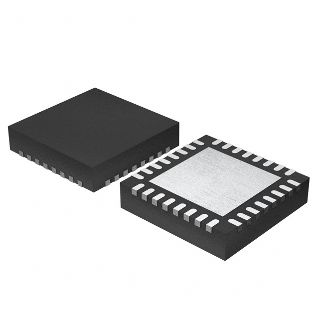
The 9TCS1083 is available in a 32-pin QFN package and is
available for commercial temperature range.
Applications
•
•
•
•
•
•
•
Notebook Computers
Netbook Computers
Smartbook Computers
Consumer Portable Devices
Embedded Systems
Networking Equipment (i.e. Routers, Switches)
Network Area Storage
9TCS1083
•
•
alarms
No Calibration required in application
Diode failure detection
Support SMBUS Alert
Accuracy: ±1°C (+60°C to +100°C); ±2°C (0°C to
+100°C)
Offset register for system calibration
Series resistor cancellation feature
• High frequency or low frequency PWM outputs for use
•
•
•
•
with 4-Wire Fans
TACH inputs to measure fan speed
OS Independent Automatic Fan Speed Control based on
thermal information
Dynamic TMIN Control Mode to optimize system
acoustics
Default startup at 100% PWM for all fans for robust
operation
System Clock PLL Synthesizers
• Scalable low voltage VDD I/O (1.5V to 1.05V) to reduce
•
•
•
•
power consumption (applies to 25MHz output)
Integrated series termination resistors
Selectable – Single-ended 24MHz/27MHz/48MHz clock
output @ VDD3.3V
3 – Single ended 25MHz clock outputs (buffer out)
32.768 kHz outputs with < 1.8µA power consumption for
system RTC circuit
IDT® MOBILE ACCESS™—CLOCK SYNTHESIZER, TEMPERATURE SENSOR, & PWM FAN CONTROLLER FOR PORTABLE DEVICES
9TCS1083
REV 0.8 011612
1
�9TCS1083
MOBILE ACCESS™—CLOCK SYNTHESIZER, TEMPERATURE SENSOR, & PWM FAN CONTROLLER FOR PORTABLE DEVICES
Block Diagram
VDD_TS
Sample
Current
Regulator
RAM
11 bits
ADC
Channel 1
Analog
MUX
ALERT#
THERM#
Digital
Reference
Voltage
Fault Detect
Channel 2
Fan Controller
POR
V_bat
Power
Switch
V_3.3
SMBCLK
SMBUS
TACH
PWM
VDD_RTC
Amplitude
Control
32.768K
DCO
32K_A_IO
SMBDAT
32K_A
VDD_32KB
Fraction N
Divider
32K_B_IO
32K_B / 25M_C
VDDIO_25MA
X1
25M_IO
Xtal
X2
25M_A
VDD_25MB
GND
25M_IO
25M_B
VDD_24M
24/48M_IO
Ultra
Low Power
PLL
24M_48M
VDD_27M
27/48M_IO
27M_48M
Preferred drive strengths for single-ended outputs.
Transmission lines to load do not share series resistors.
Desktop (Zo=50Ω) and mobile (Zo=55Ω) have the same drive strength.
Number of Loads
to Drive
D.C.Drive Strength
1
2
3
Number of Loads Actually Driven.
Match Point for N
& P Voltage /
1 Load Rs = 2 Loads Rs= 3 Loads Rs =
Current (mA)
0.56 / 33
(17Ω)
0.92 / 66
(14Ω)
1.15 / 99
(11.6Ω)
33Ω [39Ω]
-
-
39Ω [43Ω]
22Ω [27Ω]
-
43Ω [43Ω]
27Ω [33Ω]
15Ω [22Ω]
IDT® MOBILE ACCESS™—CLOCK SYNTHESIZER, TEMPERATURE SENSOR, & PWM FAN CONTROLLER FOR PORTABLE DEVICES
9TCS1083
REV 0.8 011612
2
�9TCS1083
MOBILE ACCESS™—CLOCK SYNTHESIZER, TEMPERATURE SENSOR, & PWM FAN CONTROLLER FOR PORTABLE DEVICES
Thermal_DXP1
Thermal_DXN1
VBAT
VDD_32KB
SEL25*/32K_B_25M_C
GND
VDD_TS
GND_TS
Pin Assignment
32
31
30
29
28
27
26
25
Thermal_DXP2 1
24 THERM#
Thermal_DXN2 2
23 ALERT#
32K_A 3
22 VDD_RTC_OUT
VDDIO_25MA 4
21 V_3.3
9TCS1083
GND 5
20 X2
25M_A 6
19 X1
VDD_24 7
18 SMBDATA
10
11
12
13
14
15
16
GND
VDD_25MB
PWRGD/PD#
TACH
PWM
SEL_27*/27M_48M
9
25M_B
17 SMBCLK
VDD_27
SEL_24*/24M_48M 8
* Internal Pull-Up Resistor
24M/27M/48Mhz outputs require external series resistors on Board.
Power Group
Pin Number
Description
VDD
GND
4
33
VDDIO_25MA IO power
7
5
VDDIO_24 IO power
10
12
VDDIO_27
13
33
VDDIO_25B IO Power
21
33
V3.3
VDD_RTC_Out
22
27
26
25
VDD_TS power
29
27
VDDIO_32KB Power
30
27
VBAT power
* Pin33: Thermal pad (connect to GND)
IDT® MOBILE ACCESS™—CLOCK SYNTHESIZER, TEMPERATURE SENSOR, & PWM FAN CONTROLLER FOR PORTABLE DEVICES
9TCS1083
REV 0.8 011612
3
�9TCS1083
MOBILE ACCESS™—CLOCK SYNTHESIZER, TEMPERATURE SENSOR, & PWM FAN CONTROLLER FOR PORTABLE DEVICES
Pin Descriptions
PIN #
1
2
3
4
5
6
7
PIN NAME
Thermal_DXP2
Thermal_DXN2
32K_A
VDDIO_25MA
GND
25M_A
VDD_24M
TYPE
IN
IN
OUT
PWR
PWR
OUT
PWR
8
SEL_24*/24M_48M
I/O
9
SEL_27*/27M_48M
I/O
10
11
12
13
VDD_27M
25M_B
GND
VDD_25MB
PWR
OUT
PWR
PWR
14
PWRGD/PD#
IN
15
16
17
18
19
20
21
22
23
24
25
26
27
TACH
PWM
SMBCLK
SMBDAT
X1
X2
V_3.3
VDD_RTC_OUT
ALERT#
THERM#
GND_TS
VDD_TS
GND
28
SEL_25*/32KB_25M_C
29
30
31
32
33
VDD_32KB
VBAT
Thermal_DXN1
Thermal_DXP1
Thermal Pad
IN
OUT
IN
I/O
IN
OUT
PWR
OUT
OUT
OUT
PWR
PWR
PWR
I/O
PWR
PWR
IN
IN
PWR
DESCRIPTION
External thermal diode P (Channel 2)
External thermal diode N (Channel 2)
RTC clock 32.768KHz output A, typical 1V peak to peak.
Power for 25MHz_A output, typical 1.05V to 1.8V.
Ground pin
25MHz_A output, typical 1.05V to 1.8V pending on VDDIO_25MA voltage.
Power for 24/48MHz output, typical 3.3V.
24MHz enable latched input / Programmable free‐running 24/48M clock output.
SEL_24 selects the functionality of 24_48M output as the following:
1 = 24M output (Default)
0 = 48M output
27MHz enable latched input / Programmable free‐running 27/48M clock output.
SEL_27 selects the functionality of 27_48M output as the following:
1 = 27M output (default)
0 = 48M output
Power for 27/48 MHz output, typical 3.3V.
25MHz_B output, typical 3.3V peak to peak.
Ground pin
Power for LDO and main circuit.
This 3.3V LVTTL input notifies device to sample latched inputs and start up on first high assertion or
exit powerdown mode on subsequent assertions. Low enters powerdown mode.
Fan controller TACH signal input
Fan controller PWM signal output
SMBUS clock. 3.3V tolerant.
SMBUS data. 3.3V tolerant.
Crystal input. Connect to 25MHz crystal.
Crystal output. Connect to 25MHz crystal.
Power for 32K PLL core. Connect to system's 3.3V standby power rail.
Power for chipset RTC circuit.
Open drain interrupt output for SMBUS alert pin.
Open drain interrupt output for external hardware connection.
Ground pin for thermal sensor function
Power for thermal sensor function, typical 3.3V.
Ground pin
25MHz_C output select pin / Programmable free‐running 32.768khz or 25MHz clock output.
SEL_25 selects the functionality of 32K_25M output as the following:
1 = 25MHz output (Default)
0 = 32.768kHz output
Power for 32.768kHz_B output, typical 3.3V.
Power for 32kHz_A output. Connect to coin cell battery
external thermal diode N
external thermal diode P
Connect to GND.
IDT® MOBILE ACCESS™—CLOCK SYNTHESIZER, TEMPERATURE SENSOR, & PWM FAN CONTROLLER FOR PORTABLE DEVICES
9TCS1083
REV 0.8 011612
4
�9TCS1083
MOBILE ACCESS™—CLOCK SYNTHESIZER, TEMPERATURE SENSOR, & PWM FAN CONTROLLER FOR PORTABLE DEVICES
Frequency and Output Selection Tables
Clock Output Selection Table
Pin number
8
9
28
Setting
Output
L
H
L
H
L
H
48MHz
24MHz
48MHz
27MHz
32.768kHz_B
25MHz_C
Output Selection Table A
Power Supply
V_Bat
V_3.3
Remark
default, internal pull high
default, internal pull high
default, internal pull high
VDDIO_Control
VDD_32KB
VDDIO_25A
Outputs
VDD_25B
32K_A
32K_B
25M_A
25M_B
2.3~3.0
0
0
0
0
ON
OFF
OFF
OFF
2.3~3.0
0
0
0
ON
OFF
OFF
OFF
3.31
2.3~3.0
3.3
0
0
ON
ON
OFF
OFF
3.31
2.3~3.0
3.3
0
ON
ON
ON
OFF
3.31
1.05~1.52
2.3~3.0
3.3
3.3
ON
ON
ON
ON
3.31
1.05~1.52
Note 1: When V3.3 is applied, XTAL will always be ON. 32K source will switch to an analog PLL. Fan control will be ON.
Note 2: If amplitude greater than 1.5V is required on 25MHz_A output, please contact IDT support.
VDD_RTC
Vbat
V3.3
V3.3
V3.3
V3.3
Output Selection Table B
Power Supply
V_3.3
VDD_24M1
VDD_27M
Outputs
VDD_TS
24_48M
27_48M
3.3
0
0
0
OFF
OFF
3.3
3.3
0
0
ON
OFF
3.3
3.3
3.3
0
ON
ON
3.3
3.3
3.3
3.3
ON
ON
Note 1: When either VDD_24M, VDD_27M or VDD_TS is ON, V_3.3 should be ON.
Fan Control
ON
ON
ON
ON
Thermal
Sensor
OFF
OFF
OFF
ON
IDT® MOBILE ACCESS™—CLOCK SYNTHESIZER, TEMPERATURE SENSOR, & PWM FAN CONTROLLER FOR PORTABLE DEVICES
9TCS1083
REV 0.8 011612
5
�9TCS1083
MOBILE ACCESS™—CLOCK SYNTHESIZER, TEMPERATURE SENSOR, & PWM FAN CONTROLLER FOR PORTABLE DEVICES
Absolute Maximum Ratings
Stresses above the ratings listed below can cause permanent damage to the 9TCS1083. These ratings, which are standard
values for IDT commercially rated parts, are stress ratings only. Functional operation of the device at these or any other
conditions above those indicated in the operational sections of the specifications is not implied. Exposure to absolute
maximum rating conditions for extended periods can affect product reliability. Electrical parameters are guaranteed only over
the recommended operating temperature range.
PARAMETER
SYMBOL
CONDITIONS
Maximum Supply Voltage
VDDxxx
Maximum Supply Voltage
MIN
MAX
UNITS
Notes
Core/Logic Supply
3.6
V
1,2
VDDIOxxx
Core/Logic Supply
3.6
V
1,2
Maximum Input Voltage
V IH
3.3V LVCMOS Inputs
3.6
V
1,2,3
Minimum Input Voltage
V IL
Any Input
V
1,2
°
C
°C
1,2
1,2
UNITS
V
Notes
1
V
1
mA
1
ns
1
ns
1
kHz
1
UNITS
Notes
ms
1
us
1
GND - 0.5
Storage Temperature
Ts
-65
150
Case Temperature
Tcase
115
1
Unless otherwise noted, guaranteed by design and characterization, not 100% tested in production.
2
Operation under these conditions is neither implied, nor guaranteed.
3
Maximum input voltage is not to exceed maximum VDD
Electrical Characteristics–SMBus Interface
PARAMETER
SMBus Voltage
SYMBOL
VDD
V OLSMB
CONDITIONS
MIN
2.7
MAX
3.6
@ IPULLUP
Low-level Output Voltage
0.4
Current sinking at
IPULLUP
SMB Data Pin
4
VOLSMB = 0.4 V
(Max VIL - 0.15) to
SCLK/SDATA
TRI2C
1000
Clock/Data Rise Time
(Min VIH + 0.15)
(Min VIH + 0.15) to
SCLK/SDATA
T FI2C
300
Clock/Data Fall Time
(Max VIL - 0.15)
Maximum SMBus Operating
FSMBUS
Block Mode
400
Frequency
1
Unless otherwise noted, guaranteed by design and characterization, not 100% tested in production.
AC Electrical Characteristics–Input/Common Parameters
PARAMETER
SYMBOL
CONDITIONS
MIN
MAX
From VDD Power-Up or deTSTAB
Clk Stabilization
1.8
assertion of PD# to 1st clock
Differential output enable after
Tdrive_PD#
T DRPD
300
PD# de-assertion
1
Unless otherwise noted, guaranteed by design and characterization, not 100% tested in production.
IDT® MOBILE ACCESS™—CLOCK SYNTHESIZER, TEMPERATURE SENSOR, & PWM FAN CONTROLLER FOR PORTABLE DEVICES
9TCS1083
REV 0.8 011612
6
�9TCS1083
MOBILE ACCESS™—CLOCK SYNTHESIZER, TEMPERATURE SENSOR, & PWM FAN CONTROLLER FOR PORTABLE DEVICES
Electrical Characteristics–Input/Supply/Common Parameters
PARAMETER
Ambient Operating Temp
SYMBOL
Tambient
CONDITIONS
-
MIN
0
MAX
70
UNITS
°C
Supply Voltage
Supply Voltage
V_3.3
VDD_xx
Supply Voltage
Other Supply Voltages
3.135
3.135
3.465
3.465
V
V
Supply Voltage
Supply Voltage
VDDIO_25MA
V_bat
Supply Voltage
Supply Voltage
0.9975
2.3
1.575
3.465
V
V
Input High Voltage
VIHSE
Single-ended inputs
2
VDD + 0.3
V
1,4
Input Low Voltage
Low Threshold InputHigh Voltage
Low Threshold InputLow Voltage
Input Leakage Current
VILSE
Single-ended inputs
VSS - 0.3
0.8
V
1,4
VIH_FS
3.3 V +/-5%
0.7
VDD + 0.3
V
1
VIL_FS
3.3 V +/-5%
VSS - 0.3
0.35
V
1
IIN
VIN = VDD , VIN = GND
Inputs with pull or pull down
resistors
VIN = VDD , VIN = GND
-5
5
uA
1,3
-200
200
uA
1
V
1,2
0.4
V
1,2
Input Leakage Current
IINRES
Output High Voltage
VOHSE
Output Low Voltage
VOLSE
3.3V Operating Supply
Current
Full active mode, CL = Full load,
3.3V Rail
50
mA
1
IDD3.3PD#
Complete Power-Down, 3.3V Rail
10
mA
1
25
mA
1
0.1
uA
1
5
mA
1
1
mA
1
10
mA
1
0.5
uA
1
1.8
uA
1
MHz
1
7
nH
1
5
pF
1
6
pF
1
IDD3.3WOL
IDDIO_OP
IDDIO_PD#
IDDDIO_WOL
IDDIO_RTC
V_bat Operating Supply
Current
Input Frequency
Pin Inductance
Input Capacitance
2.4
IDD3.3OP
IDD3.3RTC
VDDIO Operating Supply
Current
Single-ended outputs, IOH = 1mA
Single-ended outputs, IOL = 1 mA
Notes
IDD_V_bat
Fi
WOL Mode with 25MA running,
3.3V Rail
RTC Mode with 32KA running,
3.3V Rail
Full active mode, CL = Full load,
VDDIO Rails
Complete Power-Down,
VDDIO Rails
WOL Mode with 25MA running,
VDDIO Rails
RTC Mode with only 32KA
running, VDDIO Rails
RTC Mode with 32KA running,
V_bat Rail
VDD = 3.3 V
25MHz Typical
Lpin
CIN
Logic Inputs
COUT
Output pin capacitance
1.5
X1 & X2 pins
6
pF
1
CINX
*TA = 0 - 70°C; Supply Voltage V_3.3 = VDD_TS = 3.3 V +/-5%, VDD_24M = VDD_27M = VDD_25MB = 3.3V +/- 5%,
VDD_25MA = 1.05V +/- 5%, VDD_32KB = 3.3V +/- 5%, CL = 5pF with Rs = 27Ω (unless otherwise specified)
1
Unless otherwise noted, guaranteed by design and characterization, not 100% tested in production.
2
Signal is required to be monotonic in this region.
3
Input leakage current does not include inputs with pull-up or pull-down resistors
4
3.3V referenced inputs are: SCLK, SDATA, SEL_25, SEL_24, SEL_27, PWRGD.
IDT® MOBILE ACCESS™—CLOCK SYNTHESIZER, TEMPERATURE SENSOR, & PWM FAN CONTROLLER FOR PORTABLE DEVICES
9TCS1083
REV 0.8 011612
7
�9TCS1083
MOBILE ACCESS™—CLOCK SYNTHESIZER, TEMPERATURE SENSOR, & PWM FAN CONTROLLER FOR PORTABLE DEVICES
AC Electrical Characteristics–Power Management
Output Clock Power Consumption Table
Power Supply
V_bat / V_3.3
Power Consumption @ 2' transmission line
Outputs
I_V_bat
I_V_3.3
I_VDD_32KB
I_VDD_25M
32K_A
2.3~3.3
1.8uA
0
0
0
32K_A
2.3~3.3
0
2mA
0
0
32K_A+B
2.3~3.3
0
2mA
1uA
0
32K, 25M_A
2.3~3.3
0
2mA
1uA
1mA
32K_A+B,25MA+B
2.3~3.3
0
2mA
1uA
2mA
Note: When V_3.3 is applied, XTAL will always be ON. 32K source will switch to an analog PLL.
Fan control will be ON
Power consumption @ 2' transmission line
Power Supply
V_3.3
I_V3.3
VDD_24/27/TS
I_VDD_24M
I_VDD_27M
3.3
2mA
0
0
0
3.3
2mA
3mA
0
24Mhz
3.3
2mA
3mA
1mA
24/27Mhz
3.3
2mA
3mA
1mA
24/27Mhz+Thermal+Fan
Note: When either VDD_24M, VDD_27M or VDD_TS is ON, V3.3 should be ON
I_VDD_TS
0
0
0
0.8mA
Power Switch (VBAT/V33 -> VDD_RTC)
Integrated power switch detects the VDD_RTC SW to coin battery (VBAT) or main power supply (V33).
When there is no V33 (V33=0), the SW will connect the VDD_RTC to VBAT; when V33 goes higher than 2.5V, the VDD_RTC
will be switched to V33 with no delay. After V33 goes lower than 2.3V, the VDD_RTC will be switched to VBAT, no delay.
V_bat 3.0V
V_3.3
VDD_RTC=V_bat
VDD_RTC=V_3.3
VDD_RTC=Vbat
V_bat
VDD_RTC
2.5V
2.3V
V_3.3 < 2.5V
V_3.3 < 2.3V
When VDD_RTC = VBAT, the power SW circuit consumes < 100nA.
When VDD_RTC = V33, the power consumption on VBAT needs to be “0”.
IDT® MOBILE ACCESS™—CLOCK SYNTHESIZER, TEMPERATURE SENSOR, & PWM FAN CONTROLLER FOR PORTABLE DEVICES
9TCS1083
REV 0.8 011612
8
�9TCS1083
MOBILE ACCESS™—CLOCK SYNTHESIZER, TEMPERATURE SENSOR, & PWM FAN CONTROLLER FOR PORTABLE DEVICES
Electrical Characteristics–USB48MHz
PARAMETER
Long Accuracy
Clock period
SYMBOL
ppm
Tperiod
CONDITIONS
see Tperiod min-max values
48.00MHz output nominal
MIN
-100
20.8313
Output High Voltage
VOH
IOH = -1 mA
2.4
Output Low Voltage
VOL
IOL = 1 mA
Output High Current
IOH
Output Low Current
IOL
V OH @MIN = 1.0 V
UNITS
ppm
ns
V
1
0.4
V
1
mA
1
-33
mA
1
mA
1
38
mA
1
-33
VOH@MAX = 3.135 V
VOL @ MIN = 1.95 V
MAX
100
20.8354
30
VOL @ MAX = 0.4 V
NOTES
1,2
1,2
Rising Edge Slew Rate
tSLR
Measured from 0.8 to 2.0 V
0.5
2.5
V/ns
1
Falling Edge Slew Rate
tSLR
Measured from 2.0 to 0.8 V
0.5
2.5
V/ns
1
Duty Cycle
dt1
VT = 1.5 V
45
55
%
1
Jitter, Cycle to cycle
tjcyc-cyc
VT = 1.5 V
350
ps
1
*TA = 0 - 70°C; Supply Voltage V_3.3 = VDD_TS = 3.3 V +/-5%, VDD_24M = VDD_27M = VDD_25MB = 3.3V +/- 5%,
VDD_25MA = 1.05V +/- 5%, VDD_32KB = 3.3V +/- 5%, CL = 5pF with Rs = 27Ω (unless otherwise specified)
1
Guaranteed by design and characterization, not 100% tested in production.
2
All Long Term Accuracy and Clock Period specifications are guaranteed assuming that REFOUT is at 25.000000MHz
Electrical Characteristics–24MHz
PARAMETER
Long Accuracy
Clock period
SYMBOL
ppm
Tperiod
CONDITIONS
see Tperiod min-max values
24.00MHz output nominal
MIN
-100
41.6625
Output High Voltage
VOH
IOH = -1 mA
2.4
Output Low Voltage
VOL
IOL = 1 mA
Output High Current
IOH
Output Low Current
IOL
V OH @MIN = 1.0 V
UNITS
ppm
ns
V
1
0.4
V
1
mA
1
-33
mA
1
mA
1
38
mA
1
-33
VOH@MAX = 3.135 V
VOL @ MIN = 1.95 V
MAX
100
41.6708
30
VOL @ MAX = 0.4 V
NOTES
1,2
1,2
Rising Edge Slew Rate
tSLR
Measured from 0.8 to 2.0 V
0.5
4
V/ns
1
Falling Edge Slew Rate
tSLR
Measured from 2.0 to 0.8 V
0.5
4
V/ns
1
Duty Cycle
dt1
VT = 1.5 V
45
55
%
1
Jitter, Cycle to cycle
tjcyc-cyc
VT = 1.5 V
350
ps
1
*TA = 0 - 70°C; Supply Voltage V_3.3 = VDD_TS = 3.3 V +/-5%, VDD_24M = VDD_27M = VDD_25MB = 3.3V +/- 5%,
VDD_25MA = 1.05V +/- 5%, VDD_32KB = 3.3V +/- 5%, CL = 5pF with Rs = 27Ω (unless otherwise specified)
1
Guaranteed by design and characterization, not 100% tested in production.
2
All Long Term Accuracy and Clock Period specifications are guaranteed assuming that REFOUT is at 25.000000MHz
IDT® MOBILE ACCESS™—CLOCK SYNTHESIZER, TEMPERATURE SENSOR, & PWM FAN CONTROLLER FOR PORTABLE DEVICES
9TCS1083
REV 0.8 011612
9
�9TCS1083
MOBILE ACCESS™—CLOCK SYNTHESIZER, TEMPERATURE SENSOR, & PWM FAN CONTROLLER FOR PORTABLE DEVICES
Electrical Characteristics–25M_B & 25M_C
PARAMETER
Long Accuracy
Clock period
SYMBOL
ppm
Tperiod
CONDITIONS
see Tperiod min-max values
25.00MHz output nominal
Output High Voltage
VOH
IOH = -1 mA
Output Low Voltage
VOL
IOL = 1 mA
Output High Current
IOH
V OH @MIN = 1.0 V
MIN
MAX
-100
100
39.99600 40.00400
2.4
VOL @ MIN = 1.95 V
NOTES
1,2
1,2
V
1
V
1
mA
1
mA
1
mA
1
27
mA
1
4
V/ns
1
0.4
-29
VOH@MAX = 3.135 V
UNITS
ppm
ns
-23
29
Output Low Current
IOL
Rising Edge Slew Rate
tSLR
Measured from 0.8 to 2.0 V
0.5
Falling Edge Slew Rate
tSLR
Measured from 2.0 to 0.8 V
0.5
4
V/ns
1
Duty Cycle
dt1
VT = 1.5 V
40
60
%
1
VOL @ MAX = 0.4 V
Jitter, Cycle to cycle
tjcyc-cyc
VT = 1.5 V
500
ps
1
*TA = 0 - 70°C; Supply Voltage V_3.3 = VDD_TS = 3.3 V +/-5%, VDD_24M = VDD_27M = VDD_25MB = 3.3V +/- 5%,
VDD_25MA = 1.05V +/- 5%, VDD_32KB = 3.3V +/- 5%, CL = 5pF with Rs =0Ω (unless otherwise specified)
1
Guaranteed by design and characterization, not 100% tested in production.
2
All Long Term Accuracy and Clock Period specifications are guaranteed assuming that REFOUT is at 25.000000MHz
Electrical Characteristics–25MHz_A (Low Voltage output)
PARAMETER
Long Accuracy
Clock period
SYMBOL
ppm
Tperiod
CONDITIONS
see Tperiod min-max values
25.00MHz output nominal
Output High Voltage
VOH
IOH = -1 mA
Output Low Voltage
VOL
IOL = 1 mA
Output High Current
IOH
VOH =0.83xVtop
Output Low Current
IOL
VOL = 0.13V
MIN
MAX
-100
100
39.99600 40.00400
Vtop-0.1
0.1
-3
UNITS
ppm
ns
Notes
1,2
1,2
V
1
V
1
-16
mA
1
25
mA
1
Rising Edge Slew Rate
tSLR
Measured from 20% to 80%
0.5
4
V/ns
1,3
Falling Edge Slew Rate
tFLR
Measured from 80% to 20%
0.5
4
V/ns
1,3
Duty Cycle
dt1
VT = Vtop/2
40
60
%
1,4
Jitter
tjcyc-cyc
VT = Vtop/2
500
ps
1,4
*TA = 0 - 70°C; Supply Voltage V_3.3 = VDD_TS = 3.3 V +/-5%, VDD_24M = VDD_27M = VDD_25MB = 3.3V +/- 5%,
VDD_25MA = 1.05V +/- 5%, VDD_32KB = 3.3V +/- 5%, CL = 5pF with Rs = 0Ω (unless otherwise specified)
1
Guaranteed by design and characterization, not 100% tested in production.
2
All Long Term Accuracy and Clock Period specifications are guaranteed assuming that REFOUT is at 25.000000MHz
IDT® MOBILE ACCESS™—CLOCK SYNTHESIZER, TEMPERATURE SENSOR, & PWM FAN CONTROLLER FOR PORTABLE DEVICES
9TCS1083
REV 0.8 011612
10
�9TCS1083
MOBILE ACCESS™—CLOCK SYNTHESIZER, TEMPERATURE SENSOR, & PWM FAN CONTROLLER FOR PORTABLE DEVICES
Electrical Characteristics–27MHz
PARAMETER
Long Accuracy
Clock period
SYMBOL
ppm
Tperiod
CONDITIONS
see Tperiod min-max values
27.000MHz output nominal
MIN
-50
37.0365
Output High Voltage
VOH
IOH = -1 mA
2.4
Output Low Voltage
VOL
IOL = 1 mA
Output High Current
IOH
Output Low Current
IOL
V OH @MIN = 1.0 V
MAX
50
37.0376
UNITS
ppm
ns
V
1
0.4
V
1
mA
1
-23
mA
1
mA
1
27
mA
1
-29
VOH@MAX = 3.135 V
VOL @ MIN = 1.95 V
29
VOL @ MAX = 0.4 V
Notes
1,2
1,2
Rising Edge Slew Rate
tSLR
Measured from 0.8 to 2.0 V
1
4
V/ns
1
Falling Edge Slew Rate
tFLR
Measured from 2.0 to 0.8 V
1
4
V/ns
1
Duty Cycle
dt1
VT = 1.5 V
45
55
%
1
Jitter, Cycle to cycle
tjcyc-cyc
Cycle to Cycle, VT = 1.5 V
200
ps
1
*TA = 0 - 70°C; Supply Voltage V_3.3 = VDD_TS = 3.3 V +/-5%, VDD_24M = VDD_27M = VDD_25MB = 3.3V +/- 5%,
VDD_25MA = 1.05V +/- 5%, VDD_32KB = 3.3V +/- 5%, CL = 5pF with Rs = 27Ω (unless otherwise specified)
1
Guaranteed by design and characterization, not 100% tested in production.
2
All Long Term Accuracy and Clock Period specifications are guaranteed assuming that REFOUT is at 25.000000MHz
Electrical Characteristics–32KHz_A (Low Voltage Output)
PARAMETER
Long Accuracy
Output High Voltage
SYMBOL
ppm
VOH
CONDITIONS
see Tperiod min-max values
32K_A Output
Output Low Voltage
VOL
32K_A Output
Initial Frequency Error
32KINI
0C to 70C
MIN
MAX
32.768 Typical
0.8
1.2
UNITS
kHz
V
Notes
1,2
1
0.3
+/-10
0.86
8
V
ppm
sec/day
sec
1
1
1
1
RTC Frequency Error
32KRTC_7D
7-day measurement
Rising Edge Slew Rate
tSLR
Measured from 20% to 80%
0.03 typ
V/ns
1
Falling Edge Slew Rate
tFLR
Measured from 80% to 20%
0.03 typ
V/ns
1
Duty Cycle
dt1
VT = V_bat/2
40
60
%
1
*TA = 0 - 70°C; Supply Voltage V_3.3 = VDD_TS = 3.3 V +/-5%, VDD_24M = VDD_27M = VDD_25MB = 3.3V +/- 5%,
VDD_25MA = 1.05V +/- 5%, VDD_32KB = 3.3V +/- 5%, CL = 2pF with Rs = 0Ω (unless otherwise specified)
1
Guaranteed by design and characterization, not 100% tested in production.
2
All Long Term Accuracy and Clock Period specifications are guaranteed assuming that REFOUT is at 25.000000MHz
Electrical Characteristics–32KHz_B
PARAMETER
Long Accuracy
Output High Voltage
SYMBOL
ppm
VOH
CONDITIONS
see Tperiod min-max values
32K_B Output
Output Low Voltage
VOL
32K_B Output
Initial Frequency Error
32KINI
0C to 70C
Rising Edge Slew Rate
tSLR
Measured from 20% to 80%
Falling Edge Slew Rate
tFLR
Measured from 80% to 20%
MIN
MAX
32.768 Typical
0.9975
3.465
UNITS
kHz
V
Notes
1,2
1
0.3
0.3
+/-10
0.86
2
V
ppm
sec/day
V/ns
1
1
1
1
0.3
2
V/ns
1
Duty Cycle
dt1
VT = V_bat/2
40
60
%
1
*TA = 0 - 70°C; Supply Voltage V_3.3 = VDD_TS = 3.3 V +/-5%, VDD_24M = VDD_27M = VDD_25MB = 3.3V +/- 5%,
VDD_25MA = 1.05V +/- 5%, VDD_32KB = 3.3V +/- 5%, CL = 2pF with Rs = 0Ω (unless otherwise specified)
1
Guaranteed by design and characterization, not 100% tested in production.
2
All Long Term Accuracy and Clock Period specifications are guaranteed assuming that REFOUT is at 25.000000MHz
IDT® MOBILE ACCESS™—CLOCK SYNTHESIZER, TEMPERATURE SENSOR, & PWM FAN CONTROLLER FOR PORTABLE DEVICES
9TCS1083
REV 0.8 011612
11
�9TCS1083
MOBILE ACCESS™—CLOCK SYNTHESIZER, TEMPERATURE SENSOR, & PWM FAN CONTROLLER FOR PORTABLE DEVICES
Recommended 25MHz Crystal Specification
PARAMETER
SYMBOL
CONDITIONS
Frequency Accuracy
Faccur
Frequency Error over
temperature
MAX
UNITS
NOTES
@25C
+/-10
ppm
1
Ferrt
-10C ~ 70C
+/-10
ppm
1
Frequency Aging
Faging
1 year
+/-1
ppm
1
Driver Level
DL
100
uW
1
pF
1
Crystal Load Capacitance
CL
Parallel Resonance
MIN
8pF Typical
*TA = 0 - 70°C; Supply Voltage V_3.3 = VDD_TS = 3.3 V +/-5%, VDD_24M = VDD_27M = VDD_25MB = 3.3V +/- 5%,
VDD_25MA = 1.05V +/- 5%, VDD_32KB = 3.3V +/- 5% (unless otherwise specified)
1
Guaranteed by design and characterization, not 100% tested in production.
Electrical Characteristics–Thermal Sensor Controller
PARAMETER
SYMBOL
CONDITIONS
0C