2:12 DB1200ZL Derivative for
PCIe Gen1-4 and UPI
9ZML1233E/9ZML1253E
Datasheet
Description
Features
The 9ZML1233E/9ZML1253E are second generation enhanced
performance DB1200ZL derivatives. The parts are pin-compatible
upgrades to the 9ZML1232B, while offering much improved phase
jitter performance. A fixed external feedback maintains low drift for
critical QPI/UPI applications, while each input channel has
software adjustable input-to-output delay to ease transport delay
management for today's more complex server topologies. The
9ZML1233E and 9ZML1253E have an SMBus Write Lockout pin
for increased device and system security.
▪ SMBus write lock feature; increases system security
▪ 2 software-configurable input-to-output delay lines; manage
transport delay for complex topologies
▪ LP-HCSL outputs; eliminate 24 resistors, save 41mm2 of area
(1233E)
▪ LP-HCSL outputs with 85Ω Zout; eliminate 48 resistors, save
82mm2 of area (1253E)
▪ 12 OE# pins; hardware control of each output
▪ 3 selectable SMBus addresses; multiple devices can share
same SMBus segment
PCIe Clocking Architectures
▪ Selectable PLL bandwidths; minimizes jitter peaking in
▪ Common Clocked (CC)
▪ Independent Reference (IR) with and without spread spectrum
cascaded PLL topologies
▪ Hardware/SMBus control of PLL bandwidth and bypass;
change mode without power cycle
Typical Applications
▪ Spread spectrum compatible; tracks spreading input clock for
▪
▪
▪
▪
▪ 100MHz PLL Mode; UPI support
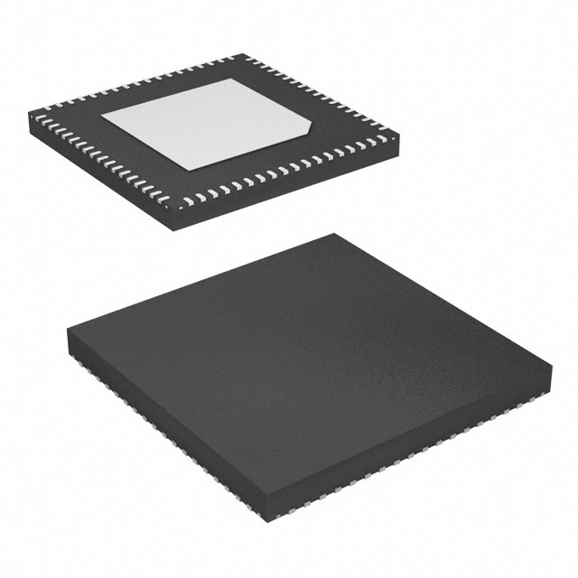
▪ 10 x 10 mm 72-VFQFPN package; small board footprint
EMI reduction
Servers
Storage
Networking
SSDs
Key Specifications
▪
▪
▪
▪
▪
▪
▪
Output Features
▪ 12 Low-Power (LP) HCSL output pairs (1233E)
▪ 12 Low-Power (LP) HCSL output pairs with 85Ω Zout (1253E)
Cycle-to-cycle jitter < 50ps
Output-to-output skew < 50ps
Input-to-output delay: 0ps default
Input-to-output delay variation < 50ps
Phase jitter: PCIe Gen4 < 0.5ps rms
Phase jitter: UPI > 9.6GB/s < 0.1ps rms
Phase jitter: IF-UPI < 1.0ps rms
Block Diagram
I2O
Delay
^SEL_A_B#
DIF_INA
DIF_INA
FBOUT_NC
Low Phase Noise
Z-PLL
(SS-Compatible)
FBOUT_NC
DIF_11
DIF_11
Bypass path
12
outputs
DIF_INB
DIF_INB
CKPWRGD_PD#
vSMB_A0_tri
vSMB_WRTLOCK
SMBDAT
SMBCLK
^OE(11:0)#
©2021 Renesas Electronics Corporation
CONTROL
^vHIBW_BYPM_LOBW#
DIF_0
NOTE: Internal series resistors are only
present on the 9ZML1253
1
DIF_0
R31DS0024EU1000 May 12, 2021
�9ZML1233E/9ZML1253E Datasheet
Contents
Description . . . . . . . . . . . . . . . . . . . . . . . . . . . . . . . . . . . . . . . . . . . . . . . . . . . . . . . . . . . . . . . . . . . . . . . . . . . . . . . . . . . . . . . . . . . . . . . . . . . . . . 1
PCIe Clocking Architectures. . . . . . . . . . . . . . . . . . . . . . . . . . . . . . . . . . . . . . . . . . . . . . . . . . . . . . . . . . . . . . . . . . . . . . . . . . . . . . . . . . . . . . . . . 1
Typical Applications . . . . . . . . . . . . . . . . . . . . . . . . . . . . . . . . . . . . . . . . . . . . . . . . . . . . . . . . . . . . . . . . . . . . . . . . . . . . . . . . . . . . . . . . . . . . . . . 1
Output Features . . . . . . . . . . . . . . . . . . . . . . . . . . . . . . . . . . . . . . . . . . . . . . . . . . . . . . . . . . . . . . . . . . . . . . . . . . . . . . . . . . . . . . . . . . . . . . . . . . 1
Features . . . . . . . . . . . . . . . . . . . . . . . . . . . . . . . . . . . . . . . . . . . . . . . . . . . . . . . . . . . . . . . . . . . . . . . . . . . . . . . . . . . . . . . . . . . . . . . . . . . . . . . . 1
Key Specifications . . . . . . . . . . . . . . . . . . . . . . . . . . . . . . . . . . . . . . . . . . . . . . . . . . . . . . . . . . . . . . . . . . . . . . . . . . . . . . . . . . . . . . . . . . . . . . . . 1
Block Diagram . . . . . . . . . . . . . . . . . . . . . . . . . . . . . . . . . . . . . . . . . . . . . . . . . . . . . . . . . . . . . . . . . . . . . . . . . . . . . . . . . . . . . . . . . . . . . . . . . . . 1
Pin Assignments. . . . . . . . . . . . . . . . . . . . . . . . . . . . . . . . . . . . . . . . . . . . . . . . . . . . . . . . . . . . . . . . . . . . . . . . . . . . . . . . . . . . . . . . . . . . . . . . . . 3
Pin Descriptions . . . . . . . . . . . . . . . . . . . . . . . . . . . . . . . . . . . . . . . . . . . . . . . . . . . . . . . . . . . . . . . . . . . . . . . . . . . . . . . . . . . . . . . . . . . . . . . . . . 3
Absolute Maximum Ratings . . . . . . . . . . . . . . . . . . . . . . . . . . . . . . . . . . . . . . . . . . . . . . . . . . . . . . . . . . . . . . . . . . . . . . . . . . . . . . . . . . . . . . . . . 6
Electrical Characteristics . . . . . . . . . . . . . . . . . . . . . . . . . . . . . . . . . . . . . . . . . . . . . . . . . . . . . . . . . . . . . . . . . . . . . . . . . . . . . . . . . . . . . . . . . . . 6
Clock Periods . . . . . . . . . . . . . . . . . . . . . . . . . . . . . . . . . . . . . . . . . . . . . . . . . . . . . . . . . . . . . . . . . . . . . . . . . . . . . . . . . . . . . . . . . . . . . . . . . . . 15
General SMBus Serial Interface Information . . . . . . . . . . . . . . . . . . . . . . . . . . . . . . . . . . . . . . . . . . . . . . . . . . . . . . . . . . . . . . . . . . . . . . . . . . . 16
How to Write . . . . . . . . . . . . . . . . . . . . . . . . . . . . . . . . . . . . . . . . . . . . . . . . . . . . . . . . . . . . . . . . . . . . . . . . . . . . . . . . . . . . . . . . . . . 16
9ZML1233E/9ZML1253E SMBus Addressing . . . . . . . . . . . . . . . . . . . . . . . . . . . . . . . . . . . . . . . . . . . . . . . . . . . . . . . . . . . . . . . . . 16
How to Read . . . . . . . . . . . . . . . . . . . . . . . . . . . . . . . . . . . . . . . . . . . . . . . . . . . . . . . . . . . . . . . . . . . . . . . . . . . . . . . . . . . . . . . . . . . 16
Package Outline Drawings . . . . . . . . . . . . . . . . . . . . . . . . . . . . . . . . . . . . . . . . . . . . . . . . . . . . . . . . . . . . . . . . . . . . . . . . . . . . . . . . . . . . . . . . . 20
Ordering Information . . . . . . . . . . . . . . . . . . . . . . . . . . . . . . . . . . . . . . . . . . . . . . . . . . . . . . . . . . . . . . . . . . . . . . . . . . . . . . . . . . . . . . . . . . . . . 20
Revision History . . . . . . . . . . . . . . . . . . . . . . . . . . . . . . . . . . . . . . . . . . . . . . . . . . . . . . . . . . . . . . . . . . . . . . . . . . . . . . . . . . . . . . . . . . . . . . . . . 21
©2021 Renesas Electronics Corporation
2
R31DS0024EU1000 May 12, 2021
�9ZML1233E/9ZML1253E Datasheet
^OE8#
^OE9#
NC
GND
DIF_8
DIF_8#
DIF_9
DIF_9#
GND
VDD
DIF_10
DIF_10#
DIF_11
DIF_11#
NC
GND
^OE10#
^OE11#
Pin Assignments
72 71 70 69 68 67 66 65 64 63 62 61 60 59 58 57 56 55
54 ^OE7#
53 ^OE6#
VDDA 1
GNDA 2
52 VDDIO
51 GND
50 DIF_7#
^SEL_A_B# 3
^vHIBW_BYPM_LOBW# 4
CKPWRGD_PD# 5
49 DIF_7
48 DIF_6#
DIF_INB 6
DIF_INB# 7
GND 8
47 DIF_6
46 GND
9ZML1233
9ZML1253
Connect EPAD to GND
VDDR 9
DIF_INA 10
DIF_INA# 11
45 VDD
44 DIF_5#
43 DIF_5
42 DIF_4#
vSADR0_tri 12
SMBDAT 13
41 DIF_4
40 VDDIO
SMBCLK 14
vSMB_WRTLOCK 15
39 GND
38 ^OE5#
37 ^OE4#
NC 16
FBOUT_NC# 17
FBOUT_NC 18
19 20 21 22 23 24 25 26 27 28 29 30 31 32 33 34 35 36
^OE3#
^OE2#
GND
NC
DIF_3#
DIF_3
DIF_2#
DIF_2
VDD
GND
DIF_1#
DIF_1
DIF_0#
DIF_0
GND
NC
^OE1#
^OE0#
^ prefix indicates internal 120kohm pull-up
v prefix indicates internal 120kohm pull-down
10 x 10 mm 72-VFQFPN 0.5mm pin pitch
Pin Descriptions
Table 1. Pin Descriptions
Number
Name
Type
Description
1
VDDA
Power
Power supply for PLL core.
2
GNDA
GND
Ground pin for the PLL core.
3
^SEL_A_B#
Input
Input to select differential input clock A or differential input clock B. This input has an
internal 120kΩ pull-up resistor.
0 = input B selected, 1 = input A selected.
4
^vHIBW_BYPM_LOBW#
5
CKPWRGD_PD#
Input
3.3V input notifies device to sample latched inputs and start up on first high assertion, or
exit Power Down Mode on subsequent assertions. Low enters Power Down Mode.
6
DIF_INB
Input
True input of differential clock.
7
DIF_INB#
Input
Complement input of differential clock.
8
GND
GND
Ground pin.
9
VDDR
Power
Power supply for differential input clock (receiver). This VDD should be treated as an analog
power rail and filtered appropriately. Nominally 3.3V.
10
DIF_INA
Input
True input of differential clock.
11
DIF_INA#
Input
Complement input of differential clock.
Latched
In
©2021 Renesas Electronics Corporation
Tri-level input to select High BW, Bypass or Low BW mode. This pin is biased to VDD/2
(Bypass Mode) with internal pull-up/pull-down resistors. See PLL Operating Mode table for
details.
3
R31DS0024EU1000 May 12, 2021
�9ZML1233E/9ZML1253E Datasheet
Table 1. Pin Descriptions (Cont.)
Number
Name
Type
Description
Input
SMBus address bit. This is a tri-level input that works in conjunction with other SADR pins,
if present, to decode SMBus Addresses. It has an internal 120kΩ pull-down resistor. See
the SMBus Addressing table.
12
vSADR0_tri
13
SMBDAT
I/O
Data pin of SMBUS circuitry.
14
SMBCLK
Input
Clock pin of SMBUS circuitry.
15
vSMB_WRTLOCK
Input
This pin prevents SMBus writes when asserted. SMBus reads are not affected. This pin has
an internal 120kΩ pull-down.
0 = SMBus writes allows, 1 = SMBus writes blocked.
16
NC
17
FBOUT_NC#
Output
Complementary half of differential feedback output. This pin should NOT be connected to
anything outside the chip. It exists to provide delay path matching to get 0 propagation
delay.
18
FBOUT_NC
Output
True half of differential feedback output. This pin should NOT be connected to anything
outside the chip. It exists to provide delay path matching to get 0 propagation delay.
19
^OE0#
Input
Active low input for enabling output 0. This pin has an internal 120kΩ pull-up resistor.
1 = disable outputs, 0 = enable outputs.
20
^OE1#
Input
Active low input for enabling output 1. This pin has an internal pull-up resistor.
1 = disable outputs, 0 = enable outputs.
21
NC
22
GND
GND
23
DIF_0
Output
HCSL true clock output.
24
DIF_0#
Output
HCSL complementary clock output.
25
DIF_1
Output
HCSL true clock output.
26
DIF_1#
Output
HCSL complementary clock output.
27
GND
GND
Ground pin.
28
VDD
Power
Power supply, nominally 3.3V.
29
DIF_2
Output
HCSL true clock output.
30
DIF_2#
Output
HCSL complementary clock output.
31
DIF_3
Output
HCSL true clock output.
32
DIF_3#
Output
HCSL complementary clock output.
33
NC
34
GND
GND
Ground pin.
35
^OE2#
Input
Active low input for enabling output 2. This pin has an internal pull-up resistor.
1 = disable outputs, 0 = enable outputs.
36
^OE3#
Input
Active low input for enabling output 3. This pin has an internal pull-up resistor.
1 = disable outputs, 0 = enable outputs.
37
^OE4#
Input
Active low input for enabling output 4. This pin has an internal pull-up resistor.
1 = disable outputs, 0 = enable outputs.
—
—
©2021 Renesas Electronics Corporation
—
No connection.
No connection.
Ground pin.
No connection.
4
R31DS0024EU1000 May 12, 2021
�9ZML1233E/9ZML1253E Datasheet
Table 1. Pin Descriptions (Cont.)
Number
Name
Type
Description
38
^OE5#
Input
Active low input for enabling output 5. This pin has an internal pull-up resistor.
1 = disable outputs, 0 = enable outputs.
39
GND
GND
Ground pin.
40
VDDIO
Power
Power supply for differential outputs.
41
DIF_4
Output
HCSL true clock output.
42
DIF_4#
Output
HCSL complementary clock output.
43
DIF_5
Output
HCSL true clock output.
44
DIF_5#
Output
HCSL complementary clock output.
45
VDD
PWR
Power supply, nominally 3.3V.
46
GND
GND
Ground pin.
47
DIF_6
Output
HCSL true clock output.
48
DIF_6#
Output
HCSL complementary clock output.
49
DIF_7
Output
HCSL true clock output.
50
DIF_7#
Output
HCSL complementary clock output.
51
GND
GND
Ground pin.
52
VDDIO
Power
Power supply for differential outputs.
53
^OE6#
Input
Active low input for enabling output 6. This pin has an internal pull-up resistor.
1 = disable outputs, 0 = enable outputs.
54
^OE7#
Input
Active low input for enabling output 7. This pin has an internal pull-up resistor.
1 = disable outputs, 0 = enable outputs.
55
^OE8#
Input
Active low input for enabling output 8. This pin has an internal pull-up resistor.
1 = disable outputs, 0 = enable outputs.
56
^OE9#
Input
Active low input for enabling output 9. This pin has an internal pull-up resistor.
1 = disable outputs, 0 = enable outputs.
57
NC
58
GND
GND
59
DIF_8
Output
HCSL true clock output.
60
DIF_8#
Output
HCSL complementary clock output.
61
DIF_9
Output
HCSL true clock output.
62
DIF_9#
Output
HCSL complementary clock output.
63
GND
GND
Ground pin.
64
VDD
Power
Power supply, nominally 3.3V.
65
DIF_10
Output
HCSL true clock output.
66
DIF_10#
Output
HCSL complementary clock output.
67
DIF_11
Output
HCSL true clock output.
68
DIF_11#
Output
HCSL complementary clock output.
—
©2021 Renesas Electronics Corporation
No connection.
Ground pin.
5
R31DS0024EU1000 May 12, 2021
�9ZML1233E/9ZML1253E Datasheet
Table 1. Pin Descriptions (Cont.)
Number
Name
Type
—
Description
69
NC
No connection.
70
GND
GND
Ground pin.
71
^OE10#
Input
Active low input for enabling output 10. This pin has an internal pull-up resistor.
1 = disable outputs, 0 = enable outputs.
72
^OE11#
Input
Active low input for enabling output 11. This pin has an internal pull-up resistor.
1 = disable outputs, 0 = enable outputs.
73
EPAD
GND
Connect to ground.
Absolute Maximum Ratings
Stresses above the ratings listed below can cause permanent damage to the 9ZML1233E/9ZML1253E. These ratings, which are
standard values for Renesas commercially rated parts, are stress ratings only. Functional operation of the device at these or any other
conditions above those indicated in the operational sections of the specifications is not implied. Exposure to absolute maximum rating
conditions for extended periods can affect product reliability. Electrical parameters are guaranteed only over the recommended operating
temperature range.
Table 2. Absolute Maximum Ratings
Parameter
Symbol
Supply Voltage
VDDx
Input Low Voltage
VIL
Input High Voltage
VIH
Except for SMBus interface.
Input High Voltage
VIHSMB
SMBus clock and data pins.
Storage Temperature
Ts
Junction Temperature
Tj
Input ESD Protection
ESD prot
1 Guaranteed
2
3
Conditions
Minimum
Typical
Maximum
Unit
Notes
3.9
V
1,2
V
1
VDD + 0.5
V
1,3
3.9
V
1
150
°
C
1
125
°C
1
V
1
Maximum
Unit
Notes
0.8
V
VDDSMB
V
0.4
V
GND-0.5
-65
Human Body Model.
2000
by design and characterization, not 100% tested in production.
Operation under these conditions is neither implied nor guaranteed.
Not to exceed 3.9V.
Electrical Characteristics
Over specified temperature and voltage ranges unless otherwise indicated; see Test Loads for loading conditions.
Table 3. SMBus Parameters
Parameter
Symbol
SMBus Input Low Voltage
VILSMB
SMBus Input High Voltage
VIHSMB
SMBus Output Low Voltage
VOLSMB
At IPULLUP.
SMBus Sink Current
IPULLUP
At VOL.
Nominal Bus Voltage
VDDSMB
©2021 Renesas Electronics Corporation
Conditions
Minimum
2.1
Typical
4
2.7
6
mA
3.6
V
1
R31DS0024EU1000 May 12, 2021
�9ZML1233E/9ZML1253E Datasheet
Table 3. SMBus Parameters (Cont.)
Parameter
Symbol
SCLK/SDATA Rise Time
tRSMB
SCLK/SDATA Fall Time
SMBus Operating Frequency
1
2
3
4
5
Conditions
Minimum
Typical
Maximum
Unit
Notes
(Max VIL - 0.15V) to (Min VIH + 0.15V).
1000
ns
1
tFSMB
(Min VIH + 0.15V) to (Max V IL - 0.15V).
300
ns
1
fMAXMB
Maximum SMBus operating frequency.
400
kHz
5
Maximum
Unit
Notes
900
mV
1
mV
1
1,2
Guaranteed by design and characterization, not 100% tested in production.
Control input must be monotonic from 20% to 80% of input swing.
Time from deassertion until outputs are > 200mV.
DIF_IN input.
The differential input clock must be running for the SMBus to be active.
Table 4. DIF_IN Clock Input Parameters
1
2
Parameter
Symbol
Conditions
Minimum
Typical
Input Crossover Voltage
VCROSS
Cross over voltage.
150
Input Swing – DIF_IN
VSWING
Differential value.
300
Input Slew Rate – DIF_IN
dv/dt
Measured differentially.
0.35
8
V/ns
Input Leakage Current
IIN
VIN = VDD , VIN = GND.
-5
5
μA
Input Duty Cycle
dtin
Measurement from differential
waveform.
45
55
%
1
Input Jitter –Cycle to Cycle
JDIFIn
Differential measurement.
0
125
ps
1
Guaranteed by design and characterization, not 100% tested in production.
Slew rate measured through ±75mV window centered around differential zero.
Table 5. Input/Supply/Common Parameters
Parameter
Supply Voltage
Symbol
Conditions
Minimum
Typical
Maximum
Unit
VDDx
Supply voltage for core and analog.
3.135
3.3
3.465
V
VDDIO
Supply voltage for differential outputs.
3.135
3.3
3.465
V
-40
85
°C
Industrial range.
Ambient Operating
Temperature
TAMB
Input High Voltage
VIH
Single-ended inputs, except SMBus, tri-level
inputs.
2
VDD + 0.3
V
Input Low Voltage
VIL
Single-ended inputs, except SMBus, tri-level
inputs.
GND - 0.3
0.8
V
Input High Voltage
VIH
Tri-level inputs (“_tri” suffix).
2.2
VDD + 0.3
V
Input Mid Voltage
VIM
Tri-level inputs (“_tri” suffix).
1.2
1.8
V
Input Low Voltage
VIL
Tri-level inputs (“_tri” suffix).
GND - 0.3
0.8
V
IIN
Single-ended inputs, VIN = GND, VIN = VDDx.
-5
5
μA
IINP
Single-ended inputs
VIN = 0 V; Inputs with internal pull-up resistors.
VIN = VDD; Inputs with internal pull-down resistors.
-100
100
μA
Input Current
©2021 Renesas Electronics Corporation
7
VDD/2
Notes
R31DS0024EU1000 May 12, 2021
�9ZML1233E/9ZML1253E Datasheet
Table 5. Input/Supply/Common Parameters (Cont.)
Parameter
Input Frequency
Pin Inductance
Symbol
FIBYP
VDD = 3.3V, Bypass Mode.
FIPLL
VDD = 3.3V, 100MHz PLL Mode.
Minimum
Typical
1
98.5
100.00
Lpin
CIN
Capacitance
Conditions
CINDIF_IN
Maximum
Unit
Notes
400
MHz
102
MHz
5
7
nH
1
Logic Inputs, except DIF_IN.
1.5
5
pF
1
DIF_IN differential clock inputs.
1.5
2.7
pF
1,4
6
pF
1
1.2
1.8
ms
1,2
30
31.6
33
kHz
4
5
10
clocks
1,2,3
85
300
μs
1,3
COUT
Output pin capacitance.
Clk Stabilization
tSTAB
From VDD power-up and after input clock
stabilization or deassertion of PD# to 1st clock.
Input SS
Modulation
Frequency PCIe
fMODINPCIe
OE# Latency
tLATOE#
DIF start after OE# assertion.
DIF stop after OE# deassertion.
Tdrive_PD#
tDRVPD
DIF output enable after PD# deassertion.
Tfall
tF
Fall time of control inputs.
5
ns
2
Trise
tR
Rise time of control inputs.
5
ns
2
Typical
Maximum
Unit
1
2
3
4
5
Allowable frequency for PCIe applications
(triangular modulation).
Guaranteed by design and characterization, not 100% tested in production.
Control input must be monotonic from 20% to 80% of input swing.
Time from deassertion until outputs are > 200mV, PLL Mode.
DIF_IN input.
This parameter reflects the operating range after locking to a 100MHz input.
Table 6. Current Consumption
Parameter
Operating Supply
Current
Power Down
Current
1
Symbol
Conditions
Minimum
Notes
IDDx
All other VDD pins, all outputs at 100MHz,
CL = 2pF; Zo = 85Ω.
22
30
mA
IDDA+R
VDDA + VDDR pins, all outputs at 100MHz,
CL = 2pF; Zo = 85Ω.
56
65
mA
IDDO
VDDIO pins, all outputs at 100MHz, CL = 2pF; Zo =
85Ω.
84
100
mA
IDDx
All other VDD pins, all outputs Low/Low.
0.9
2
mA
1
IDDA+R
VDDA + VDDR pins, all outputs Low/Low.
4.3
6
mA
1
VDDIO pins, all outputs Low/Low.
0.1
0.2
mA
1
IDDO
1
Includes VDDR if applicable.
©2021 Renesas Electronics Corporation
8
R31DS0024EU1000 May 12, 2021
�9ZML1233E/9ZML1253E Datasheet
Table 7. Skew and Differential Jitter Parameters
Parameter
Symbol
CLK_IN, DIF[x:0]
tSKEW_PLL
CLK_IN, DIF[x:0]
tPD_BYP
CLK_IN, DIF[x:0]
tDSPO_PLL
CLK_IN, DIF[x:0]
tDSPO_BYP
Conditions
Minimum
Typical
Maximum
Unit
Notes
Input-to-output skew in PLL Mode at 100MHz,
nominal temperature and voltage.
-100
-4
100
ps
1,2,4,
5,6,8
Input-to-output skew in Bypass Mode at 100MHz,
nominal temperature and voltage.
2.2
2.9
3.6
ns
1,2,3,
8
Input-to-output skew variation in PLL Mode at
100MHz, across voltage and temperature.
-50
0.0
50
ps
1,2,3,
8
Input-to-output skew variation in Bypass Mode at
100MHz, across voltage and temperature, TAMB =
0 to +70°C, default slew rate.
-250
0.0
250
ps
1,2,3,
8
Input-to-output skew variation in Bypass Mode at
100MHz, across voltage and temperature, TAMB =
-40 to +85°C, default slew rate.
-350
0.0
350
ps
1,2,3,
8
30
50
ps
1,2,3,
8
DIF[x:0]
tSKEW_ALL
Output-to-output skew across all outputs,
common to PLL and Bypass Mode, at 100MHz,
default slew rate.
PLL Jitter Peaking
jpeak-hibw
LOBW#_BYPASS_HIBW = 1.
0
1.3
2.5
dB
7,8
PLL Jitter Peaking
jpeak-lobw
LOBW#_BYPASS_HIBW = 0.
0
1.3
2
dB
7,8
PLL Bandwidth
pllHIBW
LOBW#_BYPASS_HIBW = 1.
2
2.6
4
MHz
8,9
PLL Bandwidth
pllLOBW
LOBW#_BYPASS_HIBW = 0.
0.7
1.0
1.4
MHz
8,9
Duty Cycle
tDC
Measured differentially, PLL Mode.
45
50
55
%
1
Duty Cycle Distortion
tDCD
Measured differentially, Bypass Mode at 100MHz.
-1
-0.2
0
%
1,10
Jitter, Cycle to Cycle
tjcyc-cyc
PLL Mode.
13
50
ps
1,11
Additive jitter in Bypass Mode.
0.2
5
ps
1,11
1 Measured
2 Measured
3
4
5
6
7
8
9
into fixed 2pF load cap. Input to output skew is measured at the first output edge following the corresponding input.
from differential cross-point to differential cross-point. This parameter can be tuned with external feedback path, if present.
All Bypass Mode input-to-output specs refer to the timing between an input edge and the specific output edge created by it.
This parameter is deterministic for a given device.
Measured with scope averaging on to find mean value.
This value is programmable.
Measured as maximum pass band gain. At frequencies within the loop BW, highest point of magnification is called PLL jitter peaking.
Guaranteed by design and characterization, not 100% tested in production.
Measured at 3db down or half power point.
10
11
Duty cycle distortion is the difference in duty cycle between the output and the input clock when the device is operated in Bypass Mode.
Measured from differential waveform.
©2021 Renesas Electronics Corporation
9
R31DS0024EU1000 May 12, 2021
�9ZML1233E/9ZML1253E Datasheet
Table 8. DIF HCSL/LP-HCSL Outputs
Parameter
Symbol
Slew Rate
dV/dt
Scope averaging on.
Slew Rate Matching
ΔdV/dt
Slew rate matching, scope
averaging on.
Maximum Voltage
VMAX
Minimum Voltage
VMIN
Crossing Voltage (abs)
VCROSS_ABS
Scope averaging off.
Crossing Voltage (var)
Δ-VCROSS
Scope averaging off.
1
2
Measurement on
single-ended signal using
absolute value (scope
averaging off).
Minimum
Typical
Maximum
Industry
Limits
Unit
Notes
2.0
2.8
4.0
0.6 – 4.0
V/ns
1,2,3
4
15
20
%
1,2,4,7
660
794
870
1150
-111
-49
302
367
453
250 – 550
mV
1,5,7
32
74
140
mV
1,6,7
-300
7,8
mV
7,8
Guaranteed by design and characterization, not 100% tested in production.
Measured from differential waveform.
3 Slew rate is measured
4
Conditions
through the VSWING voltage range centered around differential 0 V. This results in a ±150mV window around differential 0V.
Matching applies to rising edge rate for Clock and falling edge rate for Clock#. It is measured using a ±75mV window centered on the average
cross point where Clock rising meets Clock# falling. The median cross point is used to calculate the voltage thresholds the oscilloscope is to use
for the edge rate calculations.
5V
CROSS is defined as voltage where Clock = Clock# measured on a component test board and only applies to the differential rising edge (i.e. Clock
rising and Clock# falling).
6 The total variation
7
8
of all VCROSS measurements in any particular system. Note that this is a subset of VCROSS_MIN/MAX (VCROSS absolute) allowed.
The intent is to limit VCROSS induced modulation by setting Δ-VCROSS to be smaller than VCROSS absolute.
At default SMBus settings.
If driving a receiver with input terminations, the VMAX and VMIN values will be halved.
Table 9. Filtered Phase Jitter Parameters – PCIe Common Clocked (CC) Architectures
Parameter
Typical
Maximum
Industry
Limits
PCIe Gen1
13
30
PCIe Gen2 Low Band
10kHz < f < 1.5MHz
(PLL BW of 5–16MHz or 8–16MHz,
CDR = 5MHz).
0.25
PCIe Gen2 High Band
1.5MHz < f < Nyquist (50MHz)
(PLL BW of 5–16MHz or 8–16MHz,
CDR = 5MHz).
tjphPCIeG3-CC
tjphPCIeG4-CC
Symbol
Conditions
tjphPCIeG1-CC
tjphPCIeG2-CC
Phase Jitter,
PLL Mode
Unit
Notes
86
ps
(p-p)
1,2,3,6
0.7
3
ps
(rms)
1,2,6
1.00
1.5
3.1
ps
(rms)
1,2,6
PCIe Gen3
(PLL BW of 2–4MHz or 2–5MHz,
CDR = 10MHz).
0.24
0.35
1
ps
(rms)
1,2,6
PCIe Gen4
(PLL BW of 2–4MHz or 2–5MHz,
CDR = 10MHz).
0.24
0.35
0.5
ps
(rms)
1,2,6
©2021 Renesas Electronics Corporation
Minimum
10
R31DS0024EU1000 May 12, 2021
�9ZML1233E/9ZML1253E Datasheet
Table 9. Filtered Phase Jitter Parameters – PCIe Common Clocked (CC) Architectures (Cont.)
Parameter
Symbol
Conditions
tjphPCIeG1-CC
Notes
0.05
ps
(p-p)
1,2,3,
4,6
0.00
0.05
ps
(rms)
1,2,3,
4,6
PCIe Gen2 High Band
1.5MHz < f < Nyquist (50MHz)
(PLL BW of 5–16MHz or 8–16MHz,
CDR = 5MHz).
0.00
0.05
ps
(rms)
1,2,3,
4,6
tjphPCIeG3-CC
PCIe Gen3
(PLL BW of 2–4MHz or 2–5MHz,
CDR = 10MHz).
0.00
0.05
ps
(rms)
1,2,3,
4,6
tjphPCIeG4-CC
PCIe Gen4
(PLL BW of 2–4MHz or 2–5MHz,
CDR = 10MHz).
0.00
0.05
ps
(rms)
1,2,3,
4,6
Unit
Notes
Additive Phase
Jitter, Bypass
Mode
Typical
Maximum
PCIe Gen1
0.0
PCIe Gen2 Low Band
10kHz < f < 1.5MHz
(PLL BW of 5–16MHz or 8–16MHz,
CDR = 5MHz).
Industry
Limits
Unit
tjphPCIeG2-CC
Minimum
Not
Applicable
Table 10. Filtered Phase Jitter Parameters – PCIe Independent Reference (IR) Architectures
Typical
Maximum
Industry
Limits
PCIe Gen2
(PLL BW of 16MHz, CDR = 5MHz).
0.8
1.2
2
ps
(rms)
1,2,5
tjphPCIeG3-SRIS
PCIe Gen3
(PLL BW of 2–4MHz, CDR = 10MHz).
0.64
0.68
0.7
ps
(rms)
1,2,5
tjphPCIeG2-SRIS
PCIe Gen2
(PLL BW of 16MHz, CDR = 5MHz).
0.00
0.02
ps
(rms)
2,4,5
tjphPCIeG3-SRIS
PCIe Gen3
(PLL BW of 2–4MHz, CDR = 10MHz).
0.00
0.02
ps
(rms)
2,4,5
Parameter
Phase Jitter,
PLL Mode
Additive
Phase Jitter,
Bypass Mode
Symbol
Conditions
tjphPCIeG2-SRIS
Minimum
Not
Applicable
Notes for PCIe Filtered Phase Jitter tables:
1
2
3
Applies to all differential outputs when driven by 9SQL495x or equivalent, guaranteed by design and characterization.
Calculated from Intel-supplied clock jitter tool, when driven by 9SQL495x or equivalent with spread on and off.
Sample size of at least 100K cycles. This figure extrapolates to 108ps pk-pk at 1M cycles for a BER of 1–12 .
4 For RMS values,
5
jitter.
additive jitter is calculated by solving the following equation for b [b = sqrt(c2 - a2)] where “a” is rms input jitter and “c” is rms total
IR is the new name for Separate Reference Independent Spread (SRIS) and Separate Reference no Spread (SRNS) PCIe clock architectures.
According to the PCIe Base Specification Rev4.0 version 0.7 draft, the jitter transfer functions and corresponding jitter limits are not defined for the
IR clock architecture. Widely accepted industry limits using widely accepted industry filters are used to populate this table. There are no accepted
filters or limits for IR clock architectures at PCIe Gen1 or Gen4 data rates.
©2021 Renesas Electronics Corporation
11
R31DS0024EU1000 May 12, 2021
�9ZML1233E/9ZML1253E Datasheet
Table 11. Filtered Phase Jitter Parameters – QPI/UPI
Parameter
Phase Jitter,
PLL Mode
Typical
Maximum
Industry
Limits
QPI and UPI
(100MHz or 133MHz, 4.8Gb/s,
6.4Gb/s 12UI).
0.15
0.3
QPI and UPI
(100MHz, 8.0Gb/s, 12UI).
0.08
QPI and UPI
(100MHz, > 9.6Gb/s, 12UI).
Symbol
Conditions
Unit
Notes
0.5
ps
(rms)
1,2
0.1
0.3
ps
(rms)
1,2
0.07
0.1
0.2
ps
(rms)
1,2
IF-UPI
0.1
0.17
0.15
0.2
1
ps
(rms)
1,4,5
QPI and UPI
(100MHz or 133MHz, 4.8Gb/s,
6.4Gb/s 12UI).
0.00
0.03
ps
(rms)
1,2,3
QPI and UPI
(100MHz, 8.0Gb/s, 12UI).
0.02
0.07
ps
(rms)
1,2,3
QPI and UPI
(100MHz, > 9.6Gb/s, 12UI).
0.02
0.06
ps
(rms)
1,2,3
IF-UPI
0.06
0.08
ps
(rms)
1,4
tjphQPI_UPI
tjphIF-UPI
Additive
Phase Jitter,
Bypass Mode
tjphQPI_UPI
tjphIF-UPI
1
2
3
4
5
Minimum
Not
Applicable
Applies to all differential outputs, guaranteed by design and characterization.
Calculated from Intel-supplied clock jitter tool, when driven by 9SQL495x or equivalent with spread on and off.
Additive jitter for RMS values is calculated by solving for b [b = sqrt(c2 - a2)] where “a” is rms input jitter and “c” is rms total jitter.
Calculated from phase noise analyzer when driven by Wenzel Associates source with Intel-specified brick-wall filter applied.
Top number is when the buffer is in Low BW mode, bottom number is when the buffer is in High BW mode.
Table 12. Unfiltered Phase Jitter Parameters – 12kHz to 20MHz
Parameter
Symbol
Conditions
Phase Jitter, PLL
Mode
tjph12k-20MHi
Phase Jitter, PLL
Mode
Additive Phase
Jitter, Bypass Mode
1
2
3
Minimum
Typical
Maximum
PLL High BW, SSC Off,
100MHz.
171
250
tjph12k-20MLo
PLL Low BW, SSC Off,
100MHz.
183
250
tjph12k-20MByp
Bypass Mode, SSC Off,
100MHz.
109
150
Industry
Limits
Not
applicable
Unit
Notes
fs
(rms)
1,2
fs
(rms)
1,2
fs
(rms)
1,2,3
Applies to all outputs when driven by Wenzel clock source.
12kHz to 20MHz brick wall filter.
For RMS values, additive jitter is calculated by solving for b [a^2 + b^2 = c^2] where “a” is rms input jitter and “c” is rms total jitter.
©2021 Renesas Electronics Corporation
12
R31DS0024EU1000 May 12, 2021
�9ZML1233E/9ZML1253E Datasheet
Power Management
Inputs
Control Bits
Outputs
CKPWRGD_PD#
DIF_IN
SMBus EN bit
DIF_x
FBOUT_NC
PLL State
0
X
X
Low/Low
Low/Low
Off
1
Running
0
Low/Low
Running
On
1
Running
Running
On
Power Connections (9ZML12xxE)
Pin Number
VDD
GND
Description
1
2
Analog PLL
9
8
Analog input
22, 27, 34, 39, 46, 51, 58, 63, 70
DIF clocks
28, 45, 64
VDDIO
40, 52
Power Connections (for pin-compatibility with 9ZML12xxB)
Pin Number
VDD
GND
Description
1
2
Analog PLL
9
8
Analog input
16, 22, 27, 34, 39, 46, 51, 58, 63,
70
DIF clocks
28, 45, 64
VDDIO
21, 33, 40, 52, 57, 69
PLL Operating Mode
HIBW_BYPM_LOBW#
Byte0[7:6]
Low (PLL Low BW)
00
Mid (Bypass)
01
High (PLL High BW)
11
Note: PLL is off in Bypass Mode.
©2021 Renesas Electronics Corporation
13
R31DS0024EU1000 May 12, 2021
�9ZML1233E/9ZML1253E Datasheet
Skew Programming
Skew[2:0]
Skew Steps
Skew (ps)
000
0
0
001
1
-416.67
010
2
-833.33
011
3
-1250.00
100
4
-1666.67
101
5
-2083.33
110
6
-2500.00
111
7
-2916.67
Figure 1. Skew Diagram
DIF_INx
tSKEW_PLL
DIF_n
Test Loads
Low-Power HCSL Output Test Load
(standard PCIe source -terminated test load )
Rs
L
CL
Test
Points
Differential Zo
CL
Rs
Table 13. Parameters for Low-Power HCSL Output Test Load
Device
Rs (Ω)
Zo (Ω)
L (inches)
CL (pF)
9ZML123x
27
85
12
2
9ZML123x
33
100
12
2
9ZML125x *
Internal
85
12
2
9ZML125x *
7.5
100
12
2
* Contact factory for versions of this device with Zo = 100Ω.
©2021 Renesas Electronics Corporation
14
R31DS0024EU1000 May 12, 2021
�9ZML1233E/9ZML1253E Datasheet
Alternate Terminations
The LP-HCSL can easily drive other logic families. See “AN-891 Driving LVPECL, LVDS, and CML Logic with “Universal” Low-Power
HCSL Outputs” for details.
Clock Periods
Table 14. Clock Periods – Differential Outputs with Spread Spectrum Disabled
Measurement Window
1 Clock
1μs
0.1s
0.1s
0.1s
1μs
1 Clock
SSC On
Center
Frequency
MHz
-c2cjitter
Abs Per
Minimum
-SSC
Short-Term
Average
Minimum
-ppm
Long-Term
Average
Minimum
0 ppm
Period
Nominal
+ppm
Long-Term
Average
Maximum
+SSC
Short-Term
Average
Maximum
+c2cjitter
Abs Per
Maximum
Unit
Notes
DIF
100.00
9.94900
—
9.99900
10.00000
10.00100
—
10.05100
ns
1,2,3
Table 15. Clock Periods – Differential Outputs with Spread Spectrum Enabled
Measurement Window
1 Clock
1μs
0.1s
0.1s
0.1s
1μs
1 Clock
SSC On
Center
Frequency
MHz
-c2cjitter
Abs Per
Minimum
-SSC
Short-Term
Average
Minimum
-ppm
Long-Term
Average
Minimum
0 ppm
Period
Nominal
+ppm
Long-Term
Average
Maximum
+SSC
Short-Term
Average
Maximum
+c2cjitter
Abs Per
Maximum
Unit
Notes
DIF
99.75
9.94906
9.99906
10.02406
10.02506
10.02607
10.05107
10.10107
ns
1,2,3
1
2
3
Guaranteed by design and characterization, not 100% tested in production.
All Long Term Accuracy specifications are guaranteed with the assumption that the input clock complies with CK420BQ accuracy requirements
(±100ppm). The buffer itself does not contribute to ppm error.
Driven by SRC output of main clock, 100MHz PLL Mode or Bypass Mode.
©2021 Renesas Electronics Corporation
15
R31DS0024EU1000 May 12, 2021
�9ZML1233E/9ZML1253E Datasheet
General SMBus Serial Interface Information
How to Write
How to Read
▪
▪
▪
▪
▪
▪
▪
▪
▪
▪
▪
▪
▪
▪
▪
▪
▪
▪
▪
▪
▪
Controller (host) sends a start bit
Controller (host) sends the write address
Renesas clock will acknowledge
Controller (host) sends the beginning byte location = N
Renesas clock will acknowledge
Controller (host) sends the byte count = X
Renesas clock will acknowledge
Controller (host) starts sending Byte N through Byte N+X-1
Renesas clock will acknowledge each byte one at a time
Controller (host) sends a stop bit
Index Block Write Operation
Controller (Host)
T
Renesas (Slave/Receiver)
Controller (host) will send a start bit
Controller (host) sends the write address
Renesas clock will acknowledge
Controller (host) sends the beginning byte location = N
Renesas clock will acknowledge
Controller (host) will send a separate start bit
Controller (host) sends the read address
Renesas clock will acknowledge
Renesas clock will send the data byte count = X
Renesas clock sends Byte N+X-1
Renesas clock sends Byte 0 through Byte X (if X(H) was
written to Byte 8)
▪ Controller (host) will need to acknowledge each byte
▪ Controller (host) will send a not acknowledge bit
▪ Controller (host) will send a stop bit
starT bit
Slave Address
WR
WRite
ACK
Index Block Read Operation
Beginning Byte = N
Controller (Host)
ACK
T
starT bit
Slave Address
WR
WRite
Data Byte Count = X
ACK
Beginning Byte N
ACK
ACK
X Byte
O
O
O
Renesas
Beginning Byte = N
ACK
O
O
O
RT
Repeat starT
Slave Address
RD
ReaD
Byte N + X - 1
ACK
ACK
stoP bit
Data Byte Count=X
ACK
9ZML1233E/9ZML1253E SMBus Addressing
SMB_A0_tri
SMBus Address (Read/Write bit = 0)
0
D8
M
DA
1
DE
Beginning Byte N
ACK
O
O
O
O
O
O
Byte N + X - 1
N
P
©2021 Renesas Electronics Corporation
X Byte
P
16
Not acknowledge
stoP bit
R31DS0024EU1000 May 12, 2021
�9ZML1233E/9ZML1253E Datasheet
SMBus Table: PLL Mode and Frequency Select Register
Byte 0
Name
Control Function
Type
0
1
Bit 7
PLL Mode bit [1]
PLL Operating Mode Rd back 1
R
Bit 6
PLL Mode bit [0]
PLL Operating Mode Rd back 0
R
Bit 5
SEL_A_B#
Input Select Readback
R
DIF_INB
DIF_INA
Pin
Bit 4
SMB_WRTLOCK_RB
SMB_WRTLOCK_Readback
R
Pin is Low
Pin is High
Pin
Bit 3
PLL_InSEL_SW_EN
Enable S/W control of PLL BW and
Input select
RW
Pin Control
SMBus Control
0
Bit 2
PLL Mode bit [1]
PLL Operating Mode 1
RW
Bit 1
PLL Mode bit [0]
PLL Operating Mode 1
RW
Bit 0
SEL_A_B#
Input Select Status or Control
RW
See PLL Operating Mode table
See PLL Operating Mode table1
DIF_INB
DIF_INA
Default
Latch
Latch
1
1
1
Note: Setting bit 3 to '1' allows the user to override the latch value from pin 5 via use of bits 2 and 1. The system may require a warm
system reset if the user changes these bits. The clock itself does not require a reset. Setting bit 3 to a '1' also allows the user to use bit 0
to control the input select.
SMBus Table: Output Disable Register
Byte 1
Name
Control Function
Type
0
Bit 7
DIF_7_En
Output Control overrides OE# pin
RW
1
Bit 6
DIF_6_En
Output Control overrides OE# pin
RW
1
Bit 5
DIF_5_En
Output Control overrides OE# pin
RW
1
Bit 4
DIF_4_En
Output Control overrides OE# pin
RW
Bit 3
DIF_3_En
Output Control overrides OE# pin
RW
Bit 2
DIF_2_En
Output Control overrides OE# pin
RW
1
Bit 1
DIF_1_En
Output Control overrides OE# pin
RW
1
Bit 0
DIF_0_En
Output Control overrides OE# pin
RW
1
Low/Low
1
Pin Control
Default
1
1
SMBus Table: Output Control Register
Byte 2
Name
Control Function
Type
0
1
Default
Bit 7
Reserved
0
Bit 6
Reserved
0
Bit 5
Reserved
0
Bit 4
Reserved
0
Bit 3
DIF_11_En
Output Control overrides OE# pin
RW
Bit 2
DIF_10_En
Output Control overrides OE# pin
RW
Bit 1
DIF_9_En
Output Control overrides OE# pin
RW
Bit 0
DIF_8_En
Output Control overrides OE# pin
RW
©2021 Renesas Electronics Corporation
17
1
Low/Low
Pin Control
1
1
1
R31DS0024EU1000 May 12, 2021
�9ZML1233E/9ZML1253E Datasheet
SMBus Table: Reserved Register
Byte 3
Name
Control Function
Type
0
1
Default
Bit 7
Reserved
0
Bit 6
Reserved
0
Bit 5
Reserved
0
Bit 4
Reserved
0
Bit 3
Reserved
0
Bit 2
Reserved
0
Bit 1
Reserved
0
Bit 0
Reserved
0
SMBus Table: Reserved Register
Byte 4
Name
Control Function
Type
0
1
Default
Bit 7
Reserved
0
Bit 6
Reserved
0
Bit 5
Reserved
0
Bit 4
Reserved
0
Bit 3
Reserved
0
Bit 2
Reserved
0
Bit 1
Reserved
0
Bit 0
Reserved
0
SMBus Table: Vendor & Revision ID Register
Byte 5
Name
Bit 7
RID3
Bit 6
RID2
Bit 5
RID1
Bit 4
RID0
R
Bit 3
VID3
R
—
—
0
Bit 2
VID2
R
—
—
0
Bit 1
VID1
R
—
—
0
Bit 0
VID0
R
—
—
1
©2021 Renesas Electronics Corporation
Control Function
Type
0
1
R
0
R
REVISION ID
18
1
E rev = 0100
R
VENDOR ID
Default
0
0
R31DS0024EU1000 May 12, 2021
�9ZML1233E/9ZML1253E Datasheet
SMBus Table: Device ID
Byte 6
Name
Control Function
Type
0
1
Default
Bit 7
Device ID 7 (MSB)
R
1
Bit 6
Device ID 6
R
1
Bit 5
Device ID 5
R
1
Bit 4
Device ID 4
R
Bit 3
Device ID 3
R
Bit 2
Device ID 2
R
1
Bit 1
Device ID 1
R
0
Bit 0
Device ID 0
R
X
X
9ZML1233 = ED
9ZML1253 = FD
1
SMBus Table: Byte Count Register
Byte 7
Name
Control Function
Type
0
1
Default
Bit 7
Reserved
0
Bit 6
Reserved
0
Bit 5
Reserved
0
Bit 4
BC4
Bit 3
BC3
Bit 2
BC2
Bit 1
BC1
Bit 0
BC0
RW
Writing to this register configures how
many bytes will be read back.
RW
RW
RW
0
Default value is 8 hex, so 9 bytes (0 to 8)
will be read back by default.
RW
1
0
0
0
SMBus Table: Output Skew Register A (when Input Clock A is selected)
Byte 8
Name
Control Function
Type
0
1
Default
Bit 7
Reserved
0
Bit 6
Reserved
0
Bit 5
Reserved
0
Bit 4
Reserved
0
Bit 3
Reserved
0
Bit 2
I2O_FB_ASkew2
Bit 1
I2O_FB_ASkew1
Bit 0
I2O_FB_ASkew0
Channel A Output delay programming
(early)
RW
RW
RW
Binary value of number of VCO periods
that outputs will be pulled earlier than
input.
0
0
0
Note: For example, at 2.4GHz, each VCO period is 416.7ps and there are 24 VCO periods in a 100MHz output. Each write to bits [2:0]
will pull the output a early by that number of VCO periods. Writing “110” four times would pull the output back in phase with the input.
Writing “001” twice will accomplish the same result as writing “010” once - pulling the output 2 VCO periods earlier.
©2021 Renesas Electronics Corporation
19
R31DS0024EU1000 May 12, 2021
�9ZML1233E/9ZML1253E Datasheet
SMBus Table: Output Skew Register A (when Input Clock B is selected)
Byte 9
Name
Control Function
Type
0
1
Default
Bit 7
Reserved
0
Bit 6
Reserved
0
Bit 5
Reserved
0
Bit 4
Reserved
0
Bit 3
Reserved
0
Bit 2
I2O_FB_BSkew2
Bit 1
I2O_FB_BSkew1
Bit 0
I2O_FB_BSkew0
Channel B Output delay programming
(early)
RW
RW
RW
Binary value of number of VCO periods
that outputs will be earlier than input.
Default is 0.
0
0
0
Note: For example, at 2.4GHz, each VCO period is 416.7ps and there are 24 VCO periods in a 100MHz output. Each write to bits [2:0]
will pull the output early by that number of VCO periods. Writing “110” four times would pull the output back in phase with the input.
Writing “001” twice will accomplish the same result as writing “010” once - pulling the output 2 VCO periods earlier.
Package Outline Drawings
The package outline drawings are located at the end of this document and are accessible from the Renesas website (see Ordering
Information for POD links). The package information is the most current data available and is subject to change without revision of this
document.
Ordering Information
Orderable Part Number
Package
9ZML1233EKILF
9ZML1233EKILFT
9ZML1253EKILF
10 × 10 mm, 0.5mm pitch 72-VFQFPN
9ZML1253EKILFT
Carrier Type
Temperature
Tray
-40° to +85°C
Tape and Reel
-40° to +85°C
Tray
-40° to +85°C
Tape and Reel
-40° to +85°C
“LF” designates PB-free configuration, RoHS compliant.
“E” is the device revision designator (will not correlate with the datasheet revision).
Marking Diagrams
▪ Line 2: part number.
▪ Line 3: “LOT” denotes the lot number.
▪ Line 4: “COO” denotes country of origin; “YYWW” denotes
the last two digits of the year and work week the part was
assembled.
©2021 Renesas Electronics Corporation
20
R31DS0024EU1000 May 12, 2021
�9ZML1233E/9ZML1253E Datasheet
Revision History
Revision Date
Description of Change
May 12, 2021
Updates to Byte 0, bit 0, bit 4, and bit 5 defaults.
May 4, 2021
▪ Updated Byte0 and footnote.
▪ Updated marking diagrams and notes.
▪ Updated Package Outline Drawings section.
April 12, 2018
Updated absolute maximum supply voltage rating and VIHSMB to 3.9V.
December 1, 2017
Removed “5V tolerant” reference in pins 13 and 14 descriptions.
May 19, 2017
Corrected typos in orderable part numbers.
May 11, 2017
▪ Updated package outline drawings to latest version.
▪ Updated Byte 6 IDs.
April 27, 2017
▪ Updated Phase Jitter, PLL Mode IF-UPI typical and maximum values.
April 21, 2017
▪ Update Features and Key Specifications.
▪ Updated PCIe Common Clocked, PCIe Separate Clocked, and QPI/UPI to latest format, added IF-UPI spec
to QPI/UPI tables.
▪ Updated Test Loads drawing to latest version.
▪ Corrected SMBus Addressing table for 1233/1253.
April 11, 2017
▪ Reverted back to original Device ID Scheme, byte 6 updated accordingly:
January 31, 2017
Initial release.
9ZML1233 = ED
9ZML1253 = FD
©2021 Renesas Electronics Corporation
21
R31DS0024EU1000 May 12, 2021
�72-VFQFPN, Package Outline Drawing
10.0 x 10.0 x 0.90 mm Body, Epad 5.95 x 5.95 mm 0.50mm Pitch
NLG72P1, PSC-4208-01, Rev 03, Page 1
© Integrated Device Technology, Inc.
�72-VFQFPN, Package Outline Drawing
10.0 x 10.0 x 0.90 mm Body, Epad 5.95 x 5.95 mm 0.50mm Pitch
NLG72P1, PSC-4208-01, Rev 03, Page 2
Package Revision History
Date Created
© Integrated Device Technology, Inc.
Rev No.
Description
Sept 3, 2019
Rev 03
Update P1 Dimension from 5. 8 to 5.95 mm SQ
May 8, 2017
Rev 02
Change Package Code QFN to VFQFPN
�IMPORTANT NOTICE AND DISCLAIMER
RENESAS ELECTRONICS CORPORATION AND ITS SUBSIDIARIES (“RENESAS”) PROVIDES TECHNICAL
SPECIFICATIONS AND RELIABILITY DATA (INCLUDING DATASHEETS), DESIGN RESOURCES (INCLUDING
REFERENCE DESIGNS), APPLICATION OR OTHER DESIGN ADVICE, WEB TOOLS, SAFETY INFORMATION, AND
OTHER RESOURCES “AS IS” AND WITH ALL FAULTS, AND DISCLAIMS ALL WARRANTIES, EXPRESS OR IMPLIED,
INCLUDING, WITHOUT LIMITATION, ANY IMPLIED WARRANTIES OF MERCHANTABILITY, FITNESS FOR A
PARTICULAR PURPOSE, OR NON-INFRINGEMENT OF THIRD PARTY INTELLECTUAL PROPERTY RIGHTS.
These resources are intended for developers skilled in the art designing with Renesas products. You are solely responsible
for (1) selecting the appropriate products for your application, (2) designing, validating, and testing your application, and (3)
ensuring your application meets applicable standards, and any other safety, security, or other requirements. These
resources are subject to change without notice. Renesas grants you permission to use these resources only for
development of an application that uses Renesas products. Other reproduction or use of these resources is strictly
prohibited. No license is granted to any other Renesas intellectual property or to any third party intellectual property.
Renesas disclaims responsibility for, and you will fully indemnify Renesas and its representatives against, any claims,
damages, costs, losses, or liabilities arising out of your use of these resources. Renesas' products are provided only subject
to Renesas' Terms and Conditions of Sale or other applicable terms agreed to in writing. No use of any Renesas resources
expands or otherwise alters any applicable warranties or warranty disclaimers for these products.
(Rev.1.0 Mar 2020)
Corporate Headquarters
Contact Information
TOYOSU FORESIA, 3-2-24 Toyosu,
Koto-ku, Tokyo 135-0061, Japan
www.renesas.com
For further information on a product, technology, the most
up-to-date version of a document, or your nearest sales
office, please visit:
www.renesas.com/contact/
Trademarks
Renesas and the Renesas logo are trademarks of Renesas
Electronics Corporation. All trademarks and registered
trademarks are the property of their respective owners.
© 2020 Renesas Electronics Corporation. All rights reserved.
�