Features
• Single 2.7V - 3.6V Supply
• Serial Peripheral Interface (SPI) Compatible
– Supports SPI Modes 0 and 3
• 70 MHz Maximum Operating Frequency
– Clock-to-Output (tV) of 6 ns Maximum
• Flexible, Optimized Erase Architecture for Code + Data Storage Applications
•
•
•
•
•
•
•
•
•
•
•
– Uniform 4-Kbyte Block Erase
– Uniform 32-Kbyte Block Erase
– Full Chip Erase
Hardware Controlled Locking of Protected Sectors via WP Pin
128-Byte Programmable OTP Security Register
Flexible Programming
– Byte/Page Program (1 to 256 Bytes)
Fast Program and Erase Times
– 2.5 ms Typical Page Program (256 Bytes) Time
– 100 ms Typical 4-Kbyte Block Erase Time
– 500 ms Typical 32-Kbyte Block Erase Time
Automatic Checking and Reporting of Erase/Program Failures
JEDEC Standard Manufacturer and Device ID Read Methodology
Low Power Dissipation
– 6 mA Active Read Current (Typical at 20 MHz)
– 5 µA Deep Power-Down Current (Typical)
Endurance: 100,000 Program/Erase Cycles
Data Retention: 20 Years
Complies with Full Industrial Temperature Range
Industry Standard Green (Pb/Halide-free/RoHS Compliant) Package Options
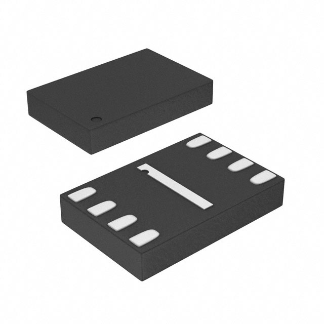
– 8-pad Ultra Thin DFN (2 x 3 x 0.6 mm)
512-Kilobit
2.7-volt
Minimum
SPI Serial Flash
Memory
AT25BCM512B
Preliminary
1. Description
The AT25BCM512B is a serial interface Flash memory device designed for use in a
wide variety of high-volume consumer based applications in which program code is
shadowed from Flash memory into embedded or external RAM for execution. The
flexible erase architecture of the AT25BCM512B, with its erase granularity as small as
4 Kbytes, makes it ideal for data storage as well, eliminating the need for additional
data storage EEPROM devices.
The erase block sizes of the AT25BCM512B have been optimized to meet the needs
of today's code and data storage applications. By optimizing the size of the erase
blocks, the memory space can be used much more efficiently. Because certain code
modules and data storage segments must reside by themselves in their own erase
regions, the wasted and unused memory space that occurs with large sectored and
large block erase Flash memory devices can be greatly reduced. This increased
memory space efficiency allows additional code routines and data storage segments
to be added while still maintaining the same overall device density.
The device also contains a specialized OTP (One-Time Programmable) Security Register that can be used for purposes such as unique device serialization, system-level
Electronic Serial Number (ESN) storage, locked key storage, etc.
Specifically designed for use in 3-volt systems, the AT25BCM512B supports read,
program, and erase operations with a supply voltage range of 2.7V to 3.6V. No separate voltage is required for programming and erasing.
3704BX–DFLASH–11/2012
�2. Pin Descriptions and Pinouts
Table 2-1.
Pin Descriptions
Asserted
State
Type
CS
CHIP SELECT: Asserting the CS pin selects the device. When the CS pin is deasserted, the
device will be deselected and normally be placed in standby mode (not Deep Power-Down
mode), and the SO pin will be in a high-impedance state. When the device is deselected,
data will not be accepted on the SI pin.
A high-to-low transition on the CS pin is required to start an operation, and a low-to-high
transition is required to end an operation. When ending an internally self-timed operation
such as a program or erase cycle, the device will not enter the standby mode until the
completion of the operation.
Low
Input
SCK
SERIAL CLOCK: This pin is used to provide a clock to the device and is used to control the
flow of data to and from the device. Command, address, and input data present on the SI pin
is always latched in on the rising edge of SCK, while output data on the SO pin is always
clocked out on the falling edge of SCK.
-
Input
SI
SERIAL INPUT: The SI pin is used to shift data into the device. The SI pin is used for all data
input including command and address sequences. Data on the SI pin is always latched in on
the rising edge of SCK.
Data present on the SI pin will be ignored whenever the device is deselected (CS is
deasserted).
-
Input
SO
SERIAL OUTPUT: The SO pin is used to shift data out from the device. Data on the SO pin
is always clocked out on the falling edge of SCK.
The SO pin will be in a high-impedance state whenever the device is deselected (CS is
deasserted).
-
Output
WP
WRITE PROTECT: The WP pin controls the hardware locking feature of the device. Please
refer to “Protection Commands and Features” on page 11 for more details on protection
features and the WP pin.
The WP pin is internally pulled-high and may be left floating if hardware controlled protection
will not be used. However, it is recommended that the WP pin also be externally connected
to VCC whenever possible.
Low
Input
Low
Input
Symbol
Name and Function
HOLD: The HOLD pin is used to temporarily pause serial communication without
deselecting or resetting the device. While the HOLD pin is asserted, transitions on the SCK
pin and data on the SI pin will be ignored, and the SO pin will be in a high-impedance state.
HOLD
The CS pin must be asserted, and the SCK pin must be in the low state in order for
a Hold condition to start. A Hold condition pauses serial communication only and
does not have an effect on internally self-timed operations such as a program or
erase cycle. Please refer to “Hold” on page 24 for additional details on the Hold
operation.
The HOLD pin is internally pulled-high and may be left floating if the Hold function will not be
used. However, it is recommended that the HOLD pin also be externally connected to VCC
whenever possible.
VCC
DEVICE POWER SUPPLY: The VCC pin is used to supply the source voltage to the device.
Operations at invalid VCC voltages may produce spurious results and should not be
attempted.
-
Power
GND
GROUND: The ground reference for the power supply. GND should be connected to the
system ground.
-
Power
2
AT25BCM512B [Preliminary]
3704BX–DFLASH–11/2012
�AT25BCM512B [Preliminary]
Figure 2-1.
8-UDFN (Top View)
CS
SO
WP
GND
1
8
2
7
3
6
4
5
VCC
HOLD
SCK
SI
3. Block Diagram
Block Diagram
CONTROL AND
PROTECTION LOGIC
CS
SCK
SI
SO
WP
HOLD
I/O BUFFERS
AND LATCHES
SRAM
DATA BUFFER
INTERFACE
CONTROL
AND
LOGIC
Y-DECODER
ADDRESS LATCH
Figure 3-1.
X-DECODER
Y-GATING
FLASH
MEMORY
ARRAY
3
3704BX–DFLASH–11/2012
�4. Memory Array
To provide the greatest flexibility, the memory array of the AT25BCM512B can be erased in
three levels of granularity including a full chip erase. The size of the erase blocks is optimized for
both code and data storage applications, allowing both code and data segments to reside in
their own erase regions. The Memory Architecture Diagram illustrates the breakdown of each
erase level.
Figure 4-1.
4
Memory Architecture Diagram
AT25BCM512B [Preliminary]
3704BX–DFLASH–11/2012
�AT25BCM512B [Preliminary]
5. Device Operation
The AT25BCM512B is controlled by a set of instructions that are sent from a host controller,
commonly referred to as the SPI Master. The SPI Master communicates with the
AT25BCM512B via the SPI bus which is comprised of four signal lines: Chip Select (CS), Serial
Clock (SCK), Serial Input (SI), and Serial Output (SO).
The SPI protocol defines a total of four modes of operation (mode 0, 1, 2, or 3) with each mode
differing in respect to the SCK polarity and phase and how the polarity and phase control the
flow of data on the SPI bus. The AT25BCM512B supports the two most common modes, SPI
Modes 0 and 3. The only difference between SPI Modes 0 and 3 is the polarity of the SCK signal
when in the inactive state (when the SPI Master is in standby mode and not transferring any
data). With SPI Modes 0 and 3, data is always latched in on the rising edge of SCK and always
output on the falling edge of SCK.
Figure 5-1.
SPI Mode 0 and 3
CS
SCK
SI
MSB
SO
LSB
MSB
LSB
6. Commands and Addressing
A valid instruction or operation must always be started by first asserting the CS pin. After the CS
pin has been asserted, the host controller must then clock out a valid 8-bit opcode on the SPI
bus. Following the opcode, instruction dependent information such as address and data bytes
would then be clocked out by the host controller. All opcode, address, and data bytes are transferred with the most-significant bit (MSB) first. An operation is ended by deasserting the CS pin.
Opcodes not supported by the AT25BCM512B will be ignored by the device and no operation
will be started. The device will continue to ignore any data presented on the SI pin until the start
of the next operation (CS pin being deasserted and then reasserted). In addition, if the CS pin is
deasserted before complete opcode and address information is sent to the device, then no operation will be performed and the device will simply return to the idle state and wait for the next
operation.
Addressing of the device requires a total of three bytes of information to be sent, representing
address bits A23-A0. Since the upper address limit of the AT25BCM512B memory array is
00FFFFh, address bits A23-A16 are always ignored by the device.
5
3704BX–DFLASH–11/2012
�Table 6-1.
Command Listing
Command
Opcode
Clock
Frequency
Address
Bytes
Dummy
Bytes
Data
Bytes
Read Commands
0Bh
0000 1011
Up to 70 MHz
3
1
1+
03h
0000 0011
Up to 33 MHz
3
0
1+
20h
0010 0000
Up to 70 MHz
3
0
0
52h
0101 0010
Up to 70 MHz
3
0
0
D8h
1101 1000
Up to 70 MHz
3
0
0
60h
0110 0000
Up to 70 MHz
0
0
0
C7h
1100 0111
Up to 70 MHz
0
0
0
Chip Erase (Legacy Command)
62h
0110 0010
Up to 70 MHz
0
0
0
Byte/Page Program (1 to 256 Bytes)
02h
0000 0010
Up to 70 MHz
3
0
1+
Write Enable
06h
0000 0110
Up to 70 MHz
0
0
0
Write Disable
04h
0000 0100
Up to 70 MHz
0
0
0
Program OTP Security Register
9Bh
1001 1011
Up to 70 MHz
3
0
1+
Read OTP Security Register
77h
0111 0111
Up to 70 MHz
3
2
1+
Read Status Register
05h
0000 0101
Up to 70 MHz
0
0
1+
Write Status Register
01h
0000 0001
Up to 70 MHz
0
0
1
Read Manufacturer and Device ID
9Fh
1001 1111
Up to 70 MHz
0
0
1 to 4
Read ID (Legacy Command)
15h
0001 0101
Up to 70 MHz
0
0
2
Deep Power-Down
B9h
1011 1001
Up to 70 MHz
0
0
0
Resume from Deep Power-Down
ABh
1010 1011
Up to 70 MHz
0
0
0
Read Array
Program and Erase Commands
Block Erase (4 Kbytes)
Block Erase (32 Kbytes)
Chip Erase
Protection Commands
Security Commands
Status Register Commands
Miscellaneous Commands
6
AT25BCM512B [Preliminary]
3704BX–DFLASH–11/2012
�AT25BCM512B [Preliminary]
7. Read Commands
7.1
Read Array
The Read Array command can be used to sequentially read a continuous stream of data from
the device by simply providing the clock signal once the initial starting address has been specified. The device incorporates an internal address counter that automatically increments on every
clock cycle.
Two opcodes (0Bh and 03h) can be used for the Read Array command. The use of each
opcode depends on the maximum clock frequency that will be used to read data from the
device. The 0Bh opcode can be used at any clock frequency up to the maximum specified by
fCLK, and the 03h opcode can be used for lower frequency read operations up to the maximum
specified by fRDLF.
To perform the Read Array operation, the CS pin must first be asserted and the appropriate
opcode (0Bh or 03h) must be clocked into the device. After the opcode has been clocked in, the
three address bytes must be clocked in to specify the starting address location of the first byte to
read within the memory array. Following the three address bytes, an additional dummy byte
needs to be clocked into the device if the 0Bh opcode is used for the Read Array operation.
After the three address bytes (and the dummy byte if using opcode 0Bh) have been clocked in,
additional clock cycles will result in data being output on the SO pin. The data is always output
with the MSB of a byte first. When the last byte (00FFFFh) of the memory array has been read,
the device will continue reading back at the beginning of the array (000000h). No delays will be
incurred when wrapping around from the end of the array to the beginning of the array.
Deasserting the CS pin will terminate the read operation and put the SO pin into a high-impedance state. The CS pin can be deasserted at any time and does not require that a full byte of
data be read.
Figure 7-1.
Read Array - 0Bh Opcode
CS
0
1
2
3
4
5
6
7
8
9
10 11 12
29 30 31 32 33 34 35 36 37 38 39 40 41 42 43 44 45 46 47 48
SCK
OPCODE
SI
0
0
0
0
1
ADDRESS BITS A23-A0
0
1
1
MSB
A
A
A
A
A
A
A
DON'T CARE
A
A
MSB
X
X
X
X
X
X
X
X
MSB
DATA BYTE 1
SO
HIGH-IMPEDANCE
D
D
D
D
D
D
MSB
Figure 7-2.
D
D
D
D
MSB
Read Array - 03h Opcode
CS
0
1
2
3
4
5
6
7
8
9
10 11 12
29 30 31 32 33 34 35 36 37 38 39 40
SCK
OPCODE
SI
0
0
0
0
0
ADDRESS BITS A23-A0
0
MSB
1
1
A
A
A
A
A
A
A
A
A
MSB
DATA BYTE 1
SO
HIGH-IMPEDANCE
D
MSB
D
D
D
D
D
D
D
D
D
MSB
7
3704BX–DFLASH–11/2012
�8. Program and Erase Commands
8.1
Byte/Page Program
The Byte/Page Program command allows anywhere from a single byte of data to 256 bytes of
data to be programmed into previously erased memory locations. An erased memory location is
one that has all eight bits set to the logical “1” state (a byte value of FFh). Before a Byte/Page
Program command can be started, the Write Enable command must have been previously
issued to the device (see “Write Enable” on page 11) to set the Write Enable Latch (WEL) bit of
the Status Register to a logical “1” state.
To perform a Byte/Page Program command, an opcode of 02h must be clocked into the device
followed by the three address bytes denoting the first byte location of the memory array to begin
programming at. After the address bytes have been clocked in, data can then be clocked into the
device and will be stored in an internal buffer.
If the starting memory address denoted by A23-A0 does not fall on an even 256-byte page
boundary (A7-A0 are not all 0), then special circumstances regarding which memory locations to
be programmed will apply. In this situation, any data that is sent to the device that goes beyond
the end of the page will wrap around back to the beginning of the same page. For example, if the
starting address denoted by A23-A0 is 0000FEh, and three bytes of data are sent to the device,
then the first two bytes of data will be programmed at addresses 0000FEh and 0000FFh while
the last byte of data will be programmed at address 000000h. The remaining bytes in the page
(addresses 000001h through 0000FDh) will not be programmed and will remain in the erased
state (FFh). In addition, if more than 256 bytes of data are sent to the device, then only the last
256 bytes sent will be latched into the internal buffer.
When the CS pin is deasserted, the device will take the data stored in the internal buffer and program it into the appropriate memory array locations based on the starting address specified by
A23-A0 and the number of data bytes sent to the device. If less than 256 bytes of data were sent
to the device, then the remaining bytes within the page will not be programmed and will remain
in the erased state (FFh). The programming of the data bytes is internally self-timed and should
take place in a time of tPP or tBP if only programming a single byte.
The three address bytes and at least one complete byte of data must be clocked into the device
before the CS pin is deasserted, and the CS pin must be deasserted on even byte boundaries
(multiples of eight bits); otherwise, the device will abort the operation and no data will be programmed into the memory array. In addition, if the memory is in the protected state (see “Block
Protection” on page 12), then the Byte/Page Program command will not be executed, and the
device will return to the idle state once the CS pin has been deasserted. The WEL bit in the Status Register will be reset back to the logical “0” state if the program cycle aborts due to an
incomplete address being sent, an incomplete byte of data being sent, the CS pin being deasserted on uneven byte boundaries, or because the memory location to be programmed is
protected.
While the device is programming, the Status Register can be read and will indicate that the
device is busy. For faster throughput, it is recommended that the Status Register be polled
rather than waiting the tBP or tPP time to determine if the data bytes have finished programming.
At some point before the program cycle completes, the WEL bit in the Status Register will be
reset back to the logical “0” state.
The device also incorporates an intelligent programming algorithm that can detect when a byte
location fails to program properly. If a programming error arises, it will be indicated by the EPE
bit in the Status Register.
8
AT25BCM512B [Preliminary]
3704BX–DFLASH–11/2012
�AT25BCM512B [Preliminary]
Figure 8-1.
Byte Program
CS
0
1
2
3
4
5
6
7
8
9
10 11 12
29 30 31 32 33 34 35 36 37 38 39
SCK
OPCODE
SI
0
0
0
0
0
ADDRESS BITS A23-A0
0
1
0
MSB
A
A
A
A
A
A
A
A
MSB
D
D
D
D
D
D
D
D
MSB
HIGH-IMPEDANCE
SO
Figure 8-2.
A
DATA IN
Page Program
CS
0
1
2
3
4
5
6
7
8
9
29 30 31 32 33 34 35 36 37 38 39
SCK
OPCODE
SI
0
0
0
0
0
ADDRESS BITS A23-A0
0
MSB
SO
8.2
1
0
A
MSB
A
A
A
A
A
DATA IN BYTE 1
D
MSB
D
D
D
D
D
D
DATA IN BYTE n
D
D
D
D
D
D
D
D
D
MSB
HIGH-IMPEDANCE
Block Erase
A block of 4 or 32 Kbytes can be erased (all bits set to the logical “1” state) in a single operation
by using one of three different opcodes for the Block Erase command. An opcode of 20h is used
for a 4-Kbyte erase, and an opcode of 52h or D8h is used for a 32-Kbyte erase. Before a Block
Erase command can be started, the Write Enable command must have been previously issued
to the device to set the WEL bit of the Status Register to a logical “1” state.
To perform a Block Erase, the CS pin must first be asserted and the appropriate opcode (20h,
52h, or D8h) must be clocked into the device. After the opcode has been clocked in, the three
address bytes specifying an address within the 4- or 32-Kbyte block to be erased must be
clocked in. Any additional data clocked into the device will be ignored. When the CS pin is deasserted, the device will erase the appropriate block. The erasing of the block is internally selftimed and should take place in a time of tBLKE.
Since the Block Erase command erases a region of bytes, the lower order address bits do not
need to be decoded by the device. Therefore, for a 4-Kbyte erase, address bits A11-A0 will be
ignored by the device and their values can be either a logical “1” or “0”. For a 32-Kbyte erase,
address bits A14-A0 will be ignored by the device. Despite the lower order address bits not
being decoded by the device, the complete three address bytes must still be clocked into the
device before the CS pin is deasserted, and the CS pin must be deasserted on an even byte
boundary (multiples of eight bits); otherwise, the device will abort the operation and no erase
operation will be performed.
If the memory is in the protected state, then the Block Erase command will not be executed, and
the device will return to the idle state once the CS pin has been deasserted.
9
3704BX–DFLASH–11/2012
�The WEL bit in the Status Register will be reset back to the logical “0” state if the erase cycle
aborts due to an incomplete address being sent, the CS pin being deasserted on uneven byte
boundaries, or because a memory location within the region to be erased is protected.
While the device is executing a successful erase cycle, the Status Register can be read and will
indicate that the device is busy. For faster throughput, it is recommended that the Status Register be polled rather than waiting the tBLKE time to determine if the device has finished erasing. At
some point before the erase cycle completes, the WEL bit in the Status Register will be reset
back to the logical “0” state.
The device also incorporates an intelligent erase algorithm that can detect when a byte location
fails to erase properly. If an erase error occurs, it will be indicated by the EPE bit in the Status
Register.
Figure 8-3.
Block Erase
CS
0
1
2
3
4
5
6
7
8
9
10 11 12
26 27 28 29 30 31
SCK
OPCODE
SI
C
C
C
C
C
C
MSB
SO
8.3
ADDRESS BITS A23-A0
C
C
A
A
A
A
A
A
A
A
A
A
A
A
MSB
HIGH-IMPEDANCE
Chip Erase
The entire memory array can be erased in a single operation by using the Chip Erase command.
Before a Chip Erase command can be started, the Write Enable command must have been previously issued to the device to set the WEL bit of the Status Register to a logical “1” state.
Three opcodes (60h, 62h, and C7h) can be used for the Chip Erase command. There is no difference in device functionality when utilizing the three opcodes, so they can be used
interchangeably. To perform a Chip Erase, one of the three opcodes must be clocked into the
device. Since the entire memory array is to be erased, no address bytes need to be clocked into
the device, and any data clocked in after the opcode will be ignored. When the CS pin is deasserted, the device will erase the entire memory array. The erasing of the device is internally selftimed and should take place in a time of tCHPE.
The complete opcode must be clocked into the device before the CS pin is deasserted, and the
CS pin must be deasserted on an even byte boundary (multiples of eight bits); otherwise, no
erase will be performed. In addition, if the memory array is in the protected state, then the Chip
Erase command will not be executed, and the device will return to the idle state once the CS pin
has been deasserted. The WEL bit in the Status Register will be reset back to the logical “0”
state if the CS pin is deasserted on uneven byte boundaries or if the memory is in the protected
state.
While the device is executing a successful erase cycle, the Status Register can be read and will
indicate that the device is busy. For faster throughput, it is recommended that the Status Register be polled rather than waiting the tCHPE time to determine if the device has finished erasing. At
10
AT25BCM512B [Preliminary]
3704BX–DFLASH–11/2012
�AT25BCM512B [Preliminary]
some point before the erase cycle completes, the WEL bit in the Status Register will be reset
back to the logical “0” state.
The device also incorporates an intelligent erase algorithm that can detect when a byte location
fails to erase properly. If an erase error occurs, it will be indicated by the EPE bit in the Status
Register.
Figure 8-4.
Chip Erase
CS
0
1
2
3
4
5
6
7
SCK
OPCODE
SI
C
C
C
C
C
C
C
C
MSB
SO
HIGH-IMPEDANCE
9. Protection Commands and Features
9.1
Write Enable
The Write Enable command is used to set the Write Enable Latch (WEL) bit in the Status Register to a logical “1” state. The WEL bit must be set before a Byte/Page Program, erase, Program
OTP Security Register, or Write Status Register command can be executed. This makes the
issuance of these commands a two step process, thereby reducing the chances of a command
being accidentally or erroneously executed. If the WEL bit in the Status Register is not set prior
to the issuance of one of these commands, then the command will not be executed.
To issue the Write Enable command, the CS pin must first be asserted and the opcode of 06h
must be clocked into the device. No address bytes need to be clocked into the device, and any
data clocked in after the opcode will be ignored. When the CS pin is deasserted, the WEL bit in
the Status Register will be set to a logical “1”. The complete opcode must be clocked into the
device before the CS pin is deasserted, and the CS pin must be deasserted on an even byte
boundary (multiples of eight bits); otherwise, the device will abort the operation and the state of
the WEL bit will not change.
Figure 9-1.
Write Enable
CS
0
1
2
3
4
5
6
7
SCK
OPCODE
SI
0
0
0
0
0
1
1
0
MSB
SO
HIGH-IMPEDANCE
11
3704BX–DFLASH–11/2012
�9.2
Write Disable
The Write Disable command is used to reset the Write Enable Latch (WEL) bit in the Status Register to the logical “0” state. With the WEL bit reset, all Byte/Page Program, erase, Program OTP
Security Register, and Write Status Register commands will not be executed. Other conditions
can also cause the WEL bit to be reset; for more details, refer to the WEL bit section of the Status Register description.
To issue the Write Disable command, the CS pin must first be asserted and the opcode of 04h
must be clocked into the device. No address bytes need to be clocked into the device, and any
data clocked in after the opcode will be ignored. When the CS pin is deasserted, the WEL bit in
the Status Register will be reset to a logical “0”. The complete opcode must be clocked into the
device before the CS pin is deasserted, and the CS pin must be deasserted on an even byte
boundary (multiples of eight bits); otherwise, the device will abort the operation and the state of
the WEL bit will not change.
Figure 9-2.
Write Disable
CS
0
1
2
3
4
5
6
7
SCK
OPCODE
SI
0
0
0
0
0
1
0
0
MSB
SO
9.3
HIGH-IMPEDANCE
Block Protection
The device can be software protected against erroneous or malicious program or erase operations by utilizing the Block Protection feature of the device. Block Protection can be enabled or
disabled by using the Write Status Register command to change the value of the Block Protection (BP0) bit in the Status Register. The following table outlines the two states of the BP0 bit
and the associated protection area.
Table 9-1.
Memory Array Protection
Protection Level
BP0
Protected Memory Address
None
0
None
Full Memory
1
00000h - 00FFFFh
When the BP0 bit of the Status Register is in the logical “1” state, the entire memory array will be
protected against program or erase operations. Any attempts to send a Byte/Page Program
command, a Block Erase command, or a Chip Erase command will be ignored by the device.
As a safeguard against accidental or erroneous protecting or unprotecting of the memory array,
the BP0 bit itself can be locked from updates by using the WP pin and the BPL (Block Protection
Locked) bit of the Status Register (see “Protected States and the Write Protect Pin” on page 13
for more details).
12
AT25BCM512B [Preliminary]
3704BX–DFLASH–11/2012
�AT25BCM512B [Preliminary]
The BP0 bit of the Status Register is a nonvolatile bit; therefore, the BP0 bit will retain its state
even after the device has been power cycled. Care should be taken to ensure that BP0 is in the
logical “1” state before powering down for those applications that wish to have the memory array
fully protected upon power up. The default state for BP0 when shipped from Adesto®is “0”.
9.4
Protected States and the Write Protect Pin
The WP pin is not linked to the memory array itself and has no direct effect on the protection status of the memory array. Instead, the WP pin, in conjunction with the BPL (Block Protection
Locked) bit in the Status Register, is used to control the hardware locking mechanism of the
device. For hardware locking to be active, two conditions must be met-the WP pin must be
asserted and the BPL bit must be in the logical “1” state.
When hardware locking is active, the Block Protection (BP0) bit is locked and the BPL bit itself is
also locked. Therefore, if the memory array is protected, it will be locked in the protected state,
and if the memory array is unprotected, it will be locked in the unprotected state. These states
cannot be changed as long as hardware locking is active, so the Write Status Register command will be ignored. In order to modify the protection status of the memory array, the WP pin
must first be deasserted, and the BPL bit in the Status Register must be reset back to the logical
“0” state using the Write Status Register command.
If the WP pin is permanently connected to GND, then once the BPL bit is set to a logical “1”, the
only way to reset the bit back to the logical “0” state is to power-cycle the device. This allows a
system to power-up with all sectors software protected but not hardware locked. Therefore, sectors can be unprotected and protected as needed and then hardware locked at a later time by
simply setting the BPL bit in the Status Register.
When the WP pin is deasserted, or if the WP pin is permanently connected to VCC, the BPL bit in
the Status Register can be set to a logical “1”, but doing so will not lock the BP0 bit.
Table 9-2 details the various protection and locking states of the device.
Table 9-2.
WP
0
0
1
1
Hardware and Software Locking
BPL
Locking
0
1
0
1
Hardware
Locked
BPL Change Allowed
BP0 and Protection Status
Can be modified from 0 to 1
BP0 bit unlocked and modifiable using
the Write Status Register command.
Memory array can be protected and
unprotected freely.
Locked
BP0 bit locked in current state. The Write
Status Register command will have no
affect. Memory array is locked in current
protected or unprotected state.
Can be modified from 0 to 1
BP0 bit unlocked and modifiable using
the Write Status Register command.
Memory array can be protected and
unprotected freely.
Can be modified from 1 to 0
BP0 bit unlocked and modifiable using
the Write Status Register command.
Memory array can be protected and
unprotected freely.
13
3704BX–DFLASH–11/2012
�10. Security Commands
10.1
Program OTP Security Register
The device contains a specialized OTP (One-Time Programmable) Security Register that can be
used for purposes such as unique device serialization, system-level Electronic Serial Number
(ESN) storage, locked key storage, etc. The OTP Security Register is independent of the main
Flash memory array and is comprised of a total of 128 bytes of memory divided into two portions. The first 64 bytes (byte locations 0 through 63) of the OTP Security Register are allocated
as a one-time user-programmable space. Once these 64 bytes have been programmed, they
cannot be erased or reprogrammed. The remaining 64 bytes of the OTP Security Register (byte
locations 64 through 127) are factory programmed by Adesto and will contain a unique value for
each device. The factory programmed data is fixed and cannot be changed.
Table 10-1.
OTP Security Register
Security Register
Byte Number
0
1
...
62
One-Time User Programmable
63
64
65
...
126
127
Factory Programmed by Adesto
The user-programmable portion of the OTP Security Register does not need to be erased before
it is programmed. In addition, the Program OTP Security Register command operates on the
entire 64-byte user-programmable portion of the OTP Security Register at one time. Once the
user-programmable space has been programmed with any number of bytes, the user-programmable space cannot be programmed again; therefore, it is not possible to only program the first
two bytes of the register and then program the remaining 62 bytes at a later time.
Before the Program OTP Security Register command can be issued, the Write Enable command
must have been previously issued to set the WEL bit in the Status Register to a logical “1”. To
program the OTP Security Register, the CS pin must first be asserted and an opcode of 9Bh
must be clocked into the device followed by the three address bytes denoting the first byte
location of the OTP Security Register to begin programming at. Since the size of the user-programmable portion of the OTP Security Register is 64 bytes, the upper order address bits do not
need to be decoded by the device. Therefore, address bits A23-A6 will be ignored by the device
and their values can be either a logical “1” or “0”. After the address bytes have been clocked in,
data can then be clocked into the device and will be stored in the internal buffer.
If the starting memory address denoted by A23-A0 does not start at the beginning of the OTP
Security Register memory space (A5-A0 are not all 0), then special circumstances regarding
which OTP Security Register locations to be programmed will apply. In this situation, any data
that is sent to the device that goes beyond the end of the 64-byte user-programmable space will
wrap around back to the beginning of the OTP Security Register. For example, if the starting
address denoted by A23-A0 is 00003Eh, and three bytes of data are sent to the device, then the
first two bytes of data will be programmed at OTP Security Register addresses 00003Eh and
00003Fh while the last byte of data will be programmed at address 000000h. The remaining
bytes in the OTP Security Register (addresses 000001h through 00003Dh) will not be programmed and will remain in the erased state (FFh). In addition, if more than 64 bytes of data are
sent to the device, then only the last 64 bytes sent will be latched into the internal buffer.
14
AT25BCM512B [Preliminary]
3704BX–DFLASH–11/2012
�AT25BCM512B [Preliminary]
When the CS pin is deasserted, the device will take the data stored in the internal buffer and program it into the appropriate OTP Security Register locations based on the starting address
specified by A23-A0 and the number of data bytes sent to the device. If less than 64 bytes of
data were sent to the device, then the remaining bytes within the OTP Security Register will not
be programmed and will remain in the erased state (FFh). The programming of the data bytes is
internally self-timed and should take place in a time of tOTPP.
The three address bytes and at least one complete byte of data must be clocked into the device
before the CS pin is deasserted, and the CS pin must be deasserted on even byte boundaries
(multiples of eight bits); otherwise, the device will abort the operation and the user-programmable portion of the OTP Security Register will not be programmed. The WEL bit in the Status
Register will be reset back to the logical “0” state if the OTP Security Register program cycle
aborts due to an incomplete address being sent, an incomplete byte of data being sent, the CS
pin being deasserted on uneven byte boundaries, or because the user-programmable portion of
the OTP Security Register was previously programmed.
While the device is programming the OTP Security Register, the Status Register can be read
and will indicate that the device is busy. For faster throughput, it is recommended that the Status
Register be polled rather than waiting the tOTPP time to determine if the data bytes have finished
programming. At some point before the OTP Security Register programming completes, the
WEL bit in the Status Register will be reset back to the logical “0” state.
If the device is powered-down during the OTP Security Register program cycle, then the contents of the 64-byte user programmable portion of the OTP Security Register cannot be
guaranteed and cannot be programmed again.
The Program OTP Security Register command utilizes the internal 256-buffer for processing.
Therefore, the contents of the buffer will be altered from its previous state when this command is
issued.
Figure 10-1. Program OTP Security Register
CS
0
1
2
3
4
5
6
7
8
9
29 30 31 32 33 34 35 36 37 38 39
SCK
OPCODE
SI
1
0
0
1
1
ADDRESS BITS A23-A0
0
MSB
SO
1
1
A
MSB
A
A
A
A
A
DATA IN BYTE 1
D
MSB
D
D
D
D
D
D
DATA IN BYTE n
D
D
D
D
D
D
D
D
D
MSB
HIGH-IMPEDANCE
15
3704BX–DFLASH–11/2012
�10.2
Read OTP Security Register
The OTP Security Register can be sequentially read in a similar fashion to the Read Array operation up to the maximum clock frequency specified by fCLK. To read the OTP Security Register,
the CS pin must first be asserted and the opcode of 77h must be clocked into the device. After
the opcode has been clocked in, the three address bytes must be clocked in to specify the starting address location of the first byte to read within the OTP Security Register. Following the
three address bytes, two dummy bytes must be clocked into the device before data can be
output.
After the three address bytes and the dummy bytes have been clocked in, additional clock
cycles will result in OTP Security Register data being output on the SO pin. When the last byte
(00007Fh) of the OTP Security Register has been read, the device will continue reading back at
the beginning of the register (000000h). No delays will be incurred when wrapping around from
the end of the register to the beginning of the register.
Deasserting the CS pin will terminate the read operation and put the SO pin into a high-impedance state. The CS pin can be deasserted at any time and does not require that a full byte of
data be read.
Figure 10-2. Read OTP Security Register
CS
0
1
2
3
4
5
6
7
8
9
10 11 12
29 30 31 32 33 34 35 36
SCK
OPCODE
SI
0
1
1
1
0
ADDRESS BITS A23-A0
1
1
1
MSB
A
A
A
A
A
MSB
A
A
DON'T CARE
A
A
X
X
X
X
X
X
X
X
X
MSB
DATA BYTE 1
SO
HIGH-IMPEDANCE
D
MSB
D
D
D
D
D
D
D
D
D
MSB
11. Status Register Commands
11.1
Read Status Register
The Status Register can be read to determine the device’s ready/busy status, as well as the status of many other functions such as Hardware Locking and Block Protection. The Status
Register can be read at any time, including during an internally self-timed program or erase
operation.
To read the Status Register, the CS pin must first be asserted and the opcode of 05h must be
clocked into the device. After the opcode has been clocked in, the device will begin outputting
Status Register data on the SO pin during every subsequent clock cycle. After the last bit (bit 0)
of the Status Register has been clocked out, the sequence will repeat itself starting again with bit
7 as long as the CS pin remains asserted and the clock pin is being pulsed. The data in the Status Register is constantly being updated, so each repeating sequence will output new data.
Deasserting the CS pin will terminate the Read Status Register operation and put the SO pin
into a high-impedance state. The CS pin can be deasserted at any time and does not require
that a full byte of data be read.
16
AT25BCM512B [Preliminary]
3704BX–DFLASH–11/2012
�AT25BCM512B [Preliminary]
Table 11-1.
Bit
Status Register Format
(1)
7
BPL
Name
Type(2)
Block Protection Locked
R/W
6
RES
Reserved for future use
R
5
EPE
Erase/Program Error
R
4
WPP
Write Protect (WP) Pin Status
3
RES
Reserved for future use
2
BP0
Block Protection
1
0
Notes:
WEL
RDY/BSY
Write Enable Latch Status
Ready/Busy Status
Description
0
BP0 bit unlocked (default).
1
BP0 bit locked in current state when WP asserted.
0
Reserved for future use.
0
Erase or program operation was successful.
1
Erase or program error detected.
0
WP is asserted.
1
WP is deasserted.
0
Reserved for future use.
0
Entire memory array is unprotected.
1
Entire memory array is protected.
0
Device is not write enabled (default).
1
Device is write enabled.
0
Device is ready.
1
Device is busy with an internal operation.
R
R
R/W
R
R
1. Only bits 7 and 2 of the Status Register can be modified when using the Write Status Register command.
2. R/W = Readable and writable
R = Readable only
11.1.1
BPL Bit
The BPL bit is used to control whether the Block Protection (BP0) bit can be modified or not.
When the BPL bit is in the logical “1” state and the WP pin is asserted, the BP0 bit will be locked
and cannot be modified. The memory array will be locked in the current protected or unprotected
state.
When the BPL bit is in the logical “0” state, the BP0 bit will be unlocked and can be modified.
The BPL bit defaults to the logical “0” state after device power-up.
The BPL bit can be modified freely whenever the WP pin is deasserted. However, if the WP pin
is asserted, then the BPL bit may only be changed from a logical “0” (BP0 bit unlocked) to a logical “1” (BP0 bit locked). In order to reset the BPL bit back to a logical “0” using the Write Status
Register command, the WP pin will have to first be deasserted.
The BPL and BP0 bits are the only bits of the Status Register that can be user modified via the
Write Status Register command.
11.1.2
EPE Bit
The EPE bit indicates whether the last erase or program operation completed successfully or
not. If at least one byte during the erase or program operation did not erase or program properly,
then the EPE bit will be set to the logical “1” state. The EPE bit will not be set if an erase or program operation aborts for any reason such as an attempt to erase or program the memory when
it is protected or if the WEL bit is not set prior to an erase or program operation. The EPE bit will
be updated after every erase and program operation.
17
3704BX–DFLASH–11/2012
�11.1.3
WPP Bit
The WPP bit can be read to determine if the WP pin has been asserted or not.
11.1.4
BP0 Bit
The BP0 bits provides feedback on the software protection status for the device. In addition, the
BP0 bit can also be modified to change the state of the software protection to allow the entire
memory array to be protected or unprotected. When the BP0 bit is in the logical “0” state, then
the entire memory array is unprotected. When the BP0 bit is in the logical “1” state, then the
entire memory array is protected against program and erase operations.
11.1.5
WEL Bit
The WEL bit indicates the current status of the internal Write Enable Latch. When the WEL bit is
in the logical “0” state, the device will not accept any Byte/Page Program, erase, Program OTP
Security Register, or Write Status Register commands. The WEL bit defaults to the logical “0”
state after a device power-up or reset operation. In addition, the WEL bit will be reset to the logical “0” state automatically under the following conditions:
• Write Disable operation completes successfully
• Write Status Register operation completes successfully or aborts
• Program OTP Security Register operation completes successfully or aborts
• Byte/Page Program operation completes successfully or aborts
• Block Erase operation completes successfully or aborts
• Chip Erase operation completes successfully or aborts
• Hold condition aborts
If the WEL bit is in the logical “1” state, it will not be reset to a logical “0” if an operation aborts
due to an incomplete or unrecognized opcode being clocked into the device before the CS pin is
deasserted. In order for the WEL bit to be reset when an operation aborts prematurely, the entire
opcode for a Byte/Page Program, erase, Program OTP Security Register, or Write Status Register command must have been clocked into the device.
11.1.6
RDY/BSY Bit
The RDY/BSY bit is used to determine whether or not an internal operation, such as a program
or erase, is in progress. To poll the RDY/BSY bit to detect the completion of a program or erase
cycle, new Status Register data must be continually clocked out of the device until the state of
the RDY/BSY bit changes from a logical “1” to a logical “0”.
Figure 11-1. Read Status Register
CS
SCK
0
1
2
3
4
5
6
7
8
9
10 11 12 13 14 15 16 17 18 19 20 21 22 23 24 25 26 27 28 29 30
OPCODE
SI
0
0
0
0
0
1
0
1
MSB
SO
HIGH-IMPEDANCE
STATUS REGISTER
DATA
D
D
D
D
D
D
STATUS REGISTER
DATA
D
D
MSB
18
D
MSB
D
D
D
D
D
STATUS REGISTER
DATA
D
D
D
D
D
D
D
D
D
D
MSB
AT25BCM512B [Preliminary]
3704BX–DFLASH–11/2012
�AT25BCM512B [Preliminary]
11.2
Write Status Register
The Write Status Register command is used to modify the BPL bit and the BP0 bit of the Status
Register. Before the Write Status Register command can be issued, the Write Enable command
must have been previously issued to set the WEL bit in the Status Register to a logical “1”.
To issue the Write Status Register command, the CS pin must first be asserted and the opcode
of 01h must be clocked into the device followed by one byte of data. The one byte of data consists of the BPL bit value, four don’t care bits, the BP0 bit value, and two additional don’t care
bits (see Table 11-2). Any additional data bytes that are sent to the device will be ignored. When
the CS pin is deasserted, the BPL bit and the BP0 bit in the Status Register will be modified, and
the WEL bit in the Status Register will be reset back to a logical “0”. The value of BP0 and the
state of the BPL bit and the WP pin before the Write Status Register command was executed
(the prior state of the BPL bit and the state of the WP pin when the CS pin is deasserted) will
determine whether or not software protection will be changed. Please refer to Section 9.4 “Protected States and the Write Protect Pin” on page 13 for more details.
The complete one byte of data must be clocked into the device before the CS pin is deasserted,
and the CS pin must be deasserted on even byte boundaries (multiples of eight bits); otherwise,
the device will abort the operation, the state of the BPL and BP0 bits will not change, memory
protection status will not change, and the WEL bit in the Status Register will be reset back to the
logical “0” state.
If the WP pin is asserted, then the BPL bit can only be set to a logical “1”. If an attempt is made
to reset the BPL bit to a logical “0” while the WP pin is asserted, then the Write Status Register
Byte command will be ignored, and the WEL bit in the Status Register will be reset back to the
logical “0” state. In order to reset the BPL bit to a logical “0”, the WP pin must be deasserted.
Table 11-2.
Write Status Register Format
Bit 7
Bit 6
Bit 5
Bit 4
Bit 3
Bit 2
Bit 1
Bit 0
BPL
X
X
X
X
BP0
X
X
Figure 11-2. Write Status Register
CS
0
1
2
3
4
5
6
7
8
9
10 11 12 13 14 15
SCK
OPCODE
SI
0
0
0
0
0
0
MSB
SO
STATUS REGISTER IN
0
1
D
X
X
X
X
D
X
X
MSB
HIGH-IMPEDANCE
19
3704BX–DFLASH–11/2012
�12. Other Commands and Functions
12.1
Read Manufacturer and Device ID
Identification information can be read from the device to enable systems to electronically query
and identify the device while it is in system. The identification method and the command opcode
comply with the JEDEC standard for “Manufacturer and Device ID Read Methodology for SPI
Compatible Serial Interface Memory Devices”. The type of information that can be read from the
device includes the JEDEC defined Manufacturer ID, the vendor specific Device ID, and the vendor specific Extended Device Information.
Since not all Flash devices are capable of operating at very high clock frequencies, applications
should be designed to read the identification information from the devices at a reasonably low
clock frequency to ensure that all devices to be used in the application can be identified properly.
Once the identification process is complete, the application can then increase the clock frequency to accommodate specific Flash devices that are capable of operating at the higher clock
frequencies.
To read the identification information, the CS pin must first be asserted and the opcode of 9Fh
must be clocked into the device. After the opcode has been clocked in, the device will begin outputting the identification data on the SO pin during the subsequent clock cycles. The first byte
that will be output will be the Manufacturer ID followed by two bytes of Device ID information.
The fourth byte output will be the Extended Device Information String Length, which will be 00h
indicating that no Extended Device Information follows. After the Extended Device Information
String Length byte is output, the SO pin will go into a high-impedance state; therefore, additional
clock cycles will have no affect on the SO pin and no data will be output. As indicated in the
JEDEC standard, reading the Extended Device Information String Length and any subsequent
data is optional.
Deasserting the CS pin will terminate the Manufacturer and Device ID read operation and put
the SO pin into a high-impedance state. The CS pin can be deasserted at any time and does not
require that a full byte of data be read.
Table 12-1.
Manufacturer and Device ID Information
Byte No.
Data Type
Value
1
Manufacturer ID
1Fh
2
Device ID (Part 1)
65h
3
Device ID (Part 2)
00h
4
Extended Device Information String Length
00h
Table 12-2.
Manufacturer and Device ID Details
Data Type
Bit 7
Bit 6
Bit 5
Bit 4
Bit 3
Bit 2
Bit 1
Bit 0
1
1
0
1
Hex
Value
Details
JEDEC Assigned Code
Manufacturer ID
0
0
0
1
1
Family Code
1
1
1
0
Sub Code
0
1
20
0
0001 1111 (1Fh for Adesto)
65h
Family Code:
Density Code:
011 (AT25F/AT25FSxxx series)
00101 (512-Kbit)
00h
Sub Code:
000 (Standard series)
Product Version: 00000
Product Version Code
Device ID (Part 2)
0
JEDEC Code:
Density Code
Device ID (Part 1)
0
1Fh
0
0
0
0
0
0
AT25BCM512B [Preliminary]
3704BX–DFLASH–11/2012
�AT25BCM512B [Preliminary]
Figure 12-1. Read Manufacturer and Device ID
CS
0
6
7
8
14 15 16
22 23 24
30 31 32
38
SCK
OPCODE
SI
9Fh
HIGH-IMPEDANCE
SO
Note: Each transition
12.2
1Fh
65h
00h
00h
MANUFACTURER ID
DEVICE ID
BYTE1
DEVICE ID
BYTE2
EXTENDED
DEVICE
INFORMATION
STRING LENGTH
shown for SI and SO represents one byte (8 bits)
Read ID (Legacy Command)
Identification information can be read from the device to enable systems to electronically query
and identify the device while it is in system. The preferred method for doing so is the JEDEC
standard “Read Manufacturer and Device ID” method described in Section 12.1 on page 20;
however, the legacy Read ID command is supported on the AT25BCM512B to enable backwards compatibility to previous generation devices.
To read the identification information, the CS pin must first be asserted and the opcode of 15h
must be clocked into the device. After the opcode has been clocked in, the device will begin outputting the identification data on the SO pin during the subsequent clock cycles. The first byte
that will be output will be the Manufacturer ID of 1Fh followed by a single byte of data representing a device code of 65h. After the device code is output, the SO pin will go into a highimpendance state; therefore, additional clock cycles will have no affect on the SO pin and no
data will be output.
Deasserting the CS pin will terminate the Read ID operation and put the SO pin into a highimpedance state. The CS pin can be deasserted at any time and does not require that a full byte
of data read.
Figure 12-2. Read ID (Legacy Command)
CS
0
1
2
3
4
5
6
7
8
9
10 11 12 13 14 15 16 17 18 19 20 21 22
SCK
OPCODE
SI
0
0
0
1
0
1
0
1
MSB
SO
HIGH-IMPEDANCE
MANUFACTURER
ID
0
MSB
0
0
1
1
1
1
DEVICE
CODE
1
0
1
1
0
0
1
0
1
MSB
21
3704BX–DFLASH–11/2012
�12.3
Deep Power-Down
During normal operation, the device will be placed in the standby mode to consume less power
as long as the CS pin remains deasserted and no internal operation is in progress. The Deep
Power-Down command offers the ability to place the device into an even lower power consumption state called the Deep Power-Down mode.
When the device is in the Deep Power-Down mode, all commands including the Read Status
Register command will be ignored with the exception of the Resume from Deep Power-Down
command. Since all commands will be ignored, the mode can be used as an extra protection
mechanism against program and erase operations.
Entering the Deep Power-Down mode is accomplished by simply asserting the CS pin, clocking
in the opcode of B9h, and then deasserting the CS pin. Any additional data clocked into the
device after the opcode will be ignored. When the CS pin is deasserted, the device will enter the
Deep Power-Down mode within the maximum time of tEDPD.
The complete opcode must be clocked in before the CS pin is deasserted, and the CS pin must
be deasserted on an even byte boundary (multiples of eight bits); otherwise, the device will abort
the operation and return to the standby mode once the CS pin is deasserted. In addition, the
device will default to the standby mode after a power-cycle.
The Deep Power-Down command will be ignored if an internally self-timed operation such as a
program or erase cycle is in progress. The Deep Power-Down command must be reissued after
the internally self-timed operation has been completed in order for the device to enter the Deep
Power-Down mode.
Figure 12-3. Deep Power-Down
CS
tEDPD
0
1
2
3
4
5
6
7
SCK
OPCODE
SI
1
0
1
1
1
0
0
1
MSB
SO
HIGH-IMPEDANCE
Active Current
ICC
Standby Mode Current
22
Deep Power-Down Mode Current
AT25BCM512B [Preliminary]
3704BX–DFLASH–11/2012
�AT25BCM512B [Preliminary]
12.4
Resume from Deep Power-Down
In order to exit the Deep Power-Down mode and resume normal device operation, the Resume
from Deep Power-Down command must be issued. The Resume from Deep Power-Down command is the only command that the device will recognized while in the Deep Power-Down mode.
To resume from the Deep Power-Down mode, the CS pin must first be asserted and opcode of
ABh must be clocked into the device. Any additional data clocked into the device after the
opcode will be ignored. When the CS pin is deasserted, the device will exit the Deep PowerDown mode within the maximum time of tRDPD and return to the standby mode. After the device
has returned to the standby mode, normal command operations such as Read Array can be
resumed.
If the complete opcode is not clocked in before the CS pin is deasserted, or if the CS pin is not
deasserted on an even byte boundary (multiples of eight bits), then the device will abort the
operation and return to the Deep Power-Down mode.
Figure 12-4. Resume from Deep Power-Down
CS
tRDPD
0
1
2
3
4
5
6
7
SCK
OPCODE
SI
1
0
1
0
1
0
1
1
MSB
SO
HIGH-IMPEDANCE
Active Current
ICC
Deep Power-Down Mode Current
Standby Mode Current
23
3704BX–DFLASH–11/2012
�12.5
Hold
The HOLD pin is used to pause the serial communication with the device without having to stop
or reset the clock sequence. The Hold mode, however, does not have an affect on any internally
self-timed operations such as a program or erase cycle. Therefore, if an erase cycle is in progress, asserting the HOLD pin will not pause the operation, and the erase cycle will continue until
it is finished.
The Hold mode can only be entered while the CS pin is asserted. The Hold mode is activated
simply by asserting the HOLD pin during the SCK low pulse. If the HOLD pin is asserted during
the SCK high pulse, then the Hold mode won’t be started until the beginning of the next SCK low
pulse. The device will remain in the Hold mode as long as the HOLD pin and CS pin are
asserted.
While in the Hold mode, the SO pin will be in a high-impedance state. In addition, both the SI pin
and the SCK pin will be ignored. The WP pin, however, can still be asserted or deasserted while
in the Hold mode.
To end the Hold mode and resume serial communication, the HOLD pin must be deasserted
during the SCK low pulse. If the HOLD pin is deasserted during the SCK high pulse, then the
Hold mode won’t end until the beginning of the next SCK low pulse.
If the CS pin is deasserted while the HOLD pin is still asserted, then any operation that may
have been started will be aborted, and the device will reset the WEL bit in the Status Register
back to the logical “0” state.
Figure 12-5. Hold Mode
CS
SCK
HOLD
Hold
24
Hold
Hold
AT25BCM512B [Preliminary]
3704BX–DFLASH–11/2012
�AT25BCM512B [Preliminary]
13. Electrical Specifications
13.1
Absolute Maximum Ratings*
*NOTICE:
Temperature under Bias ................................ -55C to +125C
Storage Temperature..................................... -65C to +150C
All Input Voltages
(including NC Pins)
with Respect to Ground .....................................-0.6V to +4.1V
All Output Voltages
with Respect to Ground .............................-0.6V to VCC + 0.5V
13.2
Stresses beyond those listed under “Absolute
Maximum Ratings” may cause permanent damage to the device. This is a stress rating only and
functional operation of the device at these or any
other conditions beyond those indicated in the
operational sections of this specification is not
implied. Exposure to absolute maximum rating
conditions for extended periods may affect device
reliability.
DC and AC Operating Range
AT25BCM512B
Operating Temperature (Case)
Ind.
-40C to 85C
VCC Power Supply
13.3
2.7V to 3.6V
DC Characteristics
Symbol
Parameter
Condition
ISB
Standby Current
IDPD
Deep Power-down Current
ICC1
Active Current, Read Operation
Min
Typ
Max
Units
CS, WP, HOLD = VCC,
all inputs at CMOS levels
25
50
µA
CS, WP, HOLD = VCC,
all inputs at CMOS levels
5
10
µA
f = 70 MHz; IOUT = 0 mA;
CS = VIL, VCC = Max
10
15
f = 66 MHz; IOUT = 0 mA;
CS = VIL, VCC = Max
9
14
f = 50 MHz; IOUT = 0 mA;
CS = VIL, VCC = Max
8
12
f = 33 MHz; IOUT = 0 mA;
CS = VIL, VCC = Max
7
10
f = 20 MHz; IOUT = 0 mA;
CS = VIL, VCC = Max
6
9
mA
ICC2
Active Current, Program Operation
CS = VCC, VCC = Max
10
15
mA
ICC3
Active Current, Erase Operation
CS = VCC, VCC = Max
12
18
mA
ILI
Input Leakage Current
VIN = CMOS levels
1
µA
ILO
Output Leakage Current
VOUT = CMOS levels
1
µA
VIL
Input Low Voltage
0.3 x VCC
V
VIH
Input High Voltage
VOL
Output Low Voltage
IOL = 1.6 mA; VCC = Min
VOH
Output High Voltage
IOH = -100 µA; VCC = Min
0.7 x VCC
V
0.4
VCC - 0.2V
V
V
25
3704BX–DFLASH–11/2012
�13.4
AC Characteristics - Maximum Clock Frequencies
AT25BCM512B
Symbol
Parameter
Min
Maximum Clock Frequency for All Operations
(excluding 03h opcode)
Maximum Clock Frequency for 03h Opcode (Read Array – Low
Frequency)
fCLK
fRDLF
13.5
Max
Units
70
MHz
33
MHz
AC Characteristics – All Other Parameters
AT25BCM512B
Symbol
Parameter
Min
tCLKH
Clock High Time
6.4
ns
tCLKL
Clock Low Time
6.4
ns
tCLKR
Clock Rise Time, Peak-to-Peak (Slew Rate)
0.1
V/ns
tCLKF(1)
Clock Fall Time, Peak-to-Peak (Slew Rate)
0.1
V/ns
tCSH
Chip Select High Time
50
ns
tCSLS
Chip Select Low Setup Time (relative to Clock)
5
ns
tCSLH
Chip Select Low Hold Time (relative to Clock)
5
ns
tCSHS
Chip Select High Setup Time (relative to Clock)
5
ns
tCSHH
Chip Select High Hold Time (relative to Clock)
5
ns
tDS
Data In Setup Time
2
ns
tDH
Data In Hold Time
3
ns
tDIS(1)
Output Disable Time
6
ns
tV(2)
Output Valid Time
6
ns
tOH
Output Hold Time
0
ns
tHLS
HOLD Low Setup Time (relative to Clock)
5
ns
tHLH
HOLD Low Hold Time (relative to Clock)
5
ns
tHHS
HOLD High Setup Time (relative to Clock)
5
ns
tHHH
HOLD High Hold Time (relative to Clock)
5
ns
tHLQZ(1)
HOLD Low to Output High-Z
6
ns
tHHQX(1)
HOLD High to Output Low-Z
6
ns
(1)
tWPS
Max
Units
(1)(3)
Write Protect Setup Time
20
ns
(1)(3)
Write Protect Hold Time
100
ns
tWPH
tEDPD
(1)
Chip Select High to Deep Power-Down
3
µs
(1)
Chip Select High to Standby Mode
8
µs
tRDPD
Notes:
1. Not 100% tested (value guaranteed by design and characterization).
2. 15 pF load at frequencies above 66 MHz, 30 pF otherwise.
3. Only applicable as a constraint for the Write Status Register command when BPL = 1.
26
AT25BCM512B [Preliminary]
3704BX–DFLASH–11/2012
�AT25BCM512B [Preliminary]
13.6
Program and Erase Characteristics
Symbol
Parameter
tPP(1)
Typ
Max
Units
Page Program Time (256 Bytes)
2.5
5.0
ms
tBP
Byte Program Time
15
tBLKE(1)
Block Erase Time
tCHPE(1)(2)
tOTPP(1)
tWRSR
Note:
(2)
Min
µs
4 Kbytes
100
250
32 Kbytes
500
1000
Chip Erase Time
0.9
2.0
sec
OTP Security Register Program Time
400
950
µs
Write Status Register Time
20
40
ms
Max
Units
ms
1. Maximum values indicate worst-case performance after 100,000 erase/program cycles.
2. Not 100% tested (value guaranteed by design and characterization).
13.7
Power-up Conditions
Symbol
Parameter
Min
tVCSL
Minimum VCC to Chip Select Low Time
500
tPUW
Power-up Device Delay Before Program or Erase Allowed
VPOR
Power-on Reset Voltage
13.8
1.5
µs
10
ms
2.5
V
Input Test Waveforms and Measurement Levels
AC
DRIVING
LEVELS
0.9VCC
VCC/2
0.1VCC
AC
MEASUREMENT
LEVEL
tR, tF < 2 ns (10% to 90%)
13.9
Output Test Load
DEVICE
UNDER
TEST
15 pF (frequencies above 66 MHz)
or
30pF
27
3704BX–DFLASH–11/2012
�14. AC Waveforms
Figure 14-1. Serial Input Timing
tCSH
CS
tCSLH
tCLKL
tCSLS
tCLKH
tCSHH
tCSHS
SCK
tDS
SI
SO
tDH
MSB
LSB
MSB
HIGH-IMPEDANCE
Figure 14-2. Serial Output Timing
CS
tCLKH
tCLKL
tDIS
SCK
SI
tOH
tV
tV
SO
Figure 14-3. WP Timing for Write Status Register Command When BPL = 1
CS
t WPH
t WPS
WP
SCK
SI
0
MSB OF
WRITE STATUS REGISTER
OPCODE
SO
28
0
0
X
MSB
LSB OF
WRITE STATUS REGISTER
DATA BYTE
MSB OF
NEXT OPCODE
HIGH-IMPEDANCE
AT25BCM512B [Preliminary]
3704BX–DFLASH–11/2012
�AT25BCM512B [Preliminary]
Figure 14-4. HOLD Timing – Serial Input
CS
SCK
tHHH
tHLS
tHLH
tHHS
tHLH
tHHS
HOLD
SI
SO
HIGH-IMPEDANCE
Figure 14-5. HOLD Timing – Serial Output
CS
SCK
tHHH
tHLS
HOLD
SI
tHLQZ
tHHQX
SO
29
3704BX–DFLASH–11/2012
�15. Ordering Information
15.1
Ordering Code Detail
A T 25 B C M 5 1 2 B – M A H – T
Designator
Shipping Carrier Option
T = Tape and reel
Product Family
Device Grade
H = Green, NiPdAu lead finish, industrial
temperature range (-40°C to +85°C)
Device Density
Package Option
MA = 8-pad, 2 x 3 x 0.6 mm UDFN
512 = 512-kilobit
Device Revision
15.2
Green Package Options (Pb/Halide-free/RoHS Compliant)
Ordering Code
Package
Lead Finish
Operating Voltage
Max. Freq.
(MHz)
AT25BCM512B-MAH-T
8MA3
NiPdAu
2.7V to 3.6V
70
Note:
Operation Range
Industrial
(-40°C to +85°C)
The shipping carrier option code is not marked on the devices.
Package Type
8MA3
30
8-pad, 2 x 3 x 0.6 mm, Thermally Enhanced Plastic Ultra Thin Dual Flat No Lead Package (UDFN)
AT25BCM512B [Preliminary]
3704BX–DFLASH–11/2012
�AT25BCM512B [Preliminary]
16. Packaging Information
16.1
8MA3 – UDFN
A
1.50 Ref.
B
8
7
6
e
5
5
8
25
E2
E
D2
A
2
3
R0.1
0.10 Ref.
PIN 1 ID
1
R0.10
4
D
L3
L
1
4
b
A1
8X
0.10mm C A B
// ccc
C
COMMON DIMENSIONS
(Unit of Measure = mm)
0.127 Ref.
8X
eee C
C
Notes: 1. All dimensions are in mm. Angles in degrees.
2. Coplanarity applies to the exposed pad as well
as the terminals. Coplanarity shall not exceed 0.05 mm.
3. Warpage shall not exceed 0.05 mm.
4. Package length/package width are considered as
special characteristic.
5. Refer to Jede MO-236/MO-252
SYMBOL
MIN
NOM
MAX
A
0.45
–
0.60
A1
0.00
–
0.05
b
0.20
–
0.30
D
1.95
2.00
2.05
D2
1.50
1.60
1.70
E
2.95
3.00
3.05
E2
0.10
0.20
0.30
e
–
0.50
–
L
0.40
0.45
0.50
L3
0.30
–
0.40
ccc
–
–
0.05
eee
–
–
0.05
NOTE
8/8/08
Package Drawing Contact:
contact@adestotech.com
TITLE
8MA3, 8-pad, 2 x 3 x 0.6 mm Body, 0.5 mm Pitch,
1.6 x 0.2 mm Exposed Pad, Saw Singulated
Thermally Enhanced Plastic Ultra Thin Dual
Flat No Lead Package (UDFN/USON)
GPC
YCQ
DRAWING NO.
8MA3
REV.
A
31
3704BX–DFLASH–11/2012
�17. Revision History
32
Revision Level – Release Date
History
AX – December 2008
Initial release
BX – November 2012
Update all Adesto Logos
AT25BCM512B [Preliminary]
3704BX–DFLASH–11/2012
�Corporate Office
California | USA
Adesto Headquarters
1250 Borregas Avenue
Sunnyvale, CA 94089
Phone: (+1) 408.400.0578
Email: contact@adestotech.com
© 2012 Adesto Technologies. All rights reserved. / Rev.: 3704BX–DFLASH–11/2012
Adesto®, the Adesto logo, CBRAM®, and DataFlash® are registered trademarks or trademarks of Adesto Technologies. All other marks are the property of their respective
owners.
Disclaimer: Adesto Technologies Corporation makes no warranty for the use of its products, other than those expressly contained in the Company's standard warranty which is detailed in Adesto's Terms
and Conditions located on the Company's web site. The Company assumes no responsibility for any errors which may appear in this document, reserves the right to change devices or specifications
detailed herein at any time without notice, and does not make any commitment to update the information contained herein. No licenses to patents or other intellectual property of Adesto are granted by the
Company in connection with the sale of Adesto products, expressly or by implication. Adesto's products are not authorized for use as critical components in life support devices or systems.
�


 工商网监
湘ICP备2023018690号
工商网监
湘ICP备2023018690号
