Following the acquisition of Adesto Technologies, Dialog Semiconductor offers memory products as part of its
product portfolio. The existing content from datasheets, including part numbers and codes should be used. Terms of
Purchase are provided on the Dialog website
https://www.dialog-semiconductor.com/general-terms-and-conditions-of-purchase
View our Dialog memory products portfolio:
www.dialog-semiconductor.com/products/memory
�PRELIMINARY DATASHEET
AT25FF161A
16 Mbit, 1.65V - 3.6V Range
SPI Serial Flash Memory with Multi-I/O Support
Features
Voltage Range: 1.65V - 3.6V
16 Mbit (2M x 8) Flash Memory
Serial Peripheral Interface (SPI) compatible
-
Supports SPI modes 0 and 3 (1-1-1)
Supports dual output operation (1-1-2)
Supports quad output operation (1-1-4)
Supports quad I/O operation (1-4-4)
Supports XiP operation (1-4-4, 0-4-4)
133 MHz maximum operating frequency
- Clock-to-output of 8 ns
Flexible, optimized erase architecture for code + data storage applications
- Uniform 4-KByte block erase
- Uniform 32-KByte block erase
- Uniform 64-KByte block erase
- Full chip erase
Flexible non-volatile block protection
1 x 128-byte factory-programmed unique identifier
3 x 128-byte, One Time Programmable (OTP) security registers
Flexible programming
- Byte/Page program (1 to 256 Bytes)
- Sequential program mode capability
Erase program suspend resume
Software controlled Reset and Terminate commands
Hardware reset option (via HOLD pin)
JEDEC hardware reset
Non-volatile status register configuration option
JEDEC standard manufacturer and device ID read methodology
Serial Flash Discoverable Parameters (SFDP) version 1.6
Low power dissipation:
- 30 µA standby current (typical)
- 8.2 µA Deep Power-Down (DPD) current (typical)
- 7 nA Ultra Deep Power Down (UDPD) current (typical)
- 8.0 mA active read current (1-1-1 — 108 MHz)
- 8.6 mA program current
- 9.6 mA erase current
User configurable and auto I/O pin drive levels
Endurance
- 100,000 program/erase cycles
Data Retention
- 20 years
Temperature Range
- -40 oC to +85 oC
Industry standard green (Pb/Halide-free/RoHS Compliant) Package Options
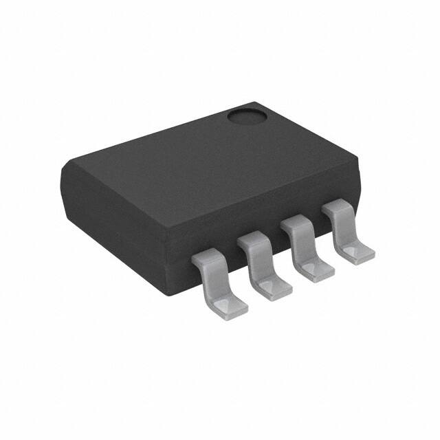
- 8-lead SOIC (150-mil)
- 8-lead SOIC (208-mil)
- 8-pad Ultra-thin DFN (2 x 3 x 0.6 mm)
- 8-ball WLCSP (3 x 2 x 3 ball matrix)
- Die in Wafer Form (DWF)
DS-AT25FF161A–182D–01-2021
�1.
Product Overview
The Adesto® AT25FF161A is a serial interface Flash memory device designed for use in a wide variety of highvolume consumer and connected applications. It is optimized for low-energy applications and can be operated using
modern Lithium battery technologies over a wide input voltage range of 1.65V - 3.6V.
The AT25FF161A is ideally suited for systems in which program code is shadowed from Flash memory into
embedded or external RAM (code shadow) for execution, and where small amounts of data are stored and updated
locally in the Flash memory.
The erase block sizes of the AT25FF161A have been optimized to meet the needs of today's code and data storage
applications. The device supports 4 KiloByte (KB), 32 KB, and 64 KB block erase operations and a full-chip erase. By
optimizing the size of the erase blocks, the memory space can be used much more efficiently.
The device contains four specialized 128-byte One-Time Programmable (OTP) security registers that can be used to
store a unique device ID and locked key storage.
Specifically designed for use in a wide variety of systems, the AT25FF161A supports read, program, and erase
operations. No separate voltage is required for programming and erasing.
Throughout this document, the term Multi-I/O is used generically to refer to all of the multiple I/O modes, including
dual, quad, and XiP.
2.
Package Pinouts
Figure 2-1 shows the package pinouts for the following packages. Note that the Die in Wafer Form (DWF) option is
not shown.
Figure 2-1. Adesto Memory Package Types
Top View
CS
1
8
VCC
SO (I/O1)
2
7
HOLD/RESET (I/O3)
WP (I/O2)
3
6
SCK
GND
4
5
SI (I/O0)
8S1 8-lead SOIC Package (0.150”)
8S2 8-lead EIAJ SOIC Package (0.208”)
Top View
CS
1
8
VCC
SO (I/O1)
2
7
HOLD/RESET (I/O3)
WP (I/O2)
3
6
SCK
GND
4
5
SI (I/O0)
8MA3 8-pad 2 x 3 Ultra-Thin DFN Package
Bottom View
9&&
&6
$�
*1'
$�
62
%�
+2/'
&�
6,
&�
:3
'�
6&.
(�
8-ball WLCSP Package
(�
AT25FF161A
DS-AT25FF161A–182D–01-2021
2
�Table of Contents
1. Product Overview . . . . . . . . . . . . . . . . . . . . . . . . . . . . . . . . . . . . . . . . . . . . . . . . . . . . . . . . . . . . . . . . . . . . 2
2. Package Pinouts . . . . . . . . . . . . . . . . . . . . . . . . . . . . . . . . . . . . . . . . . . . . . . . . . . . . . . . . . . . . . . . . . . . . . 2
3. Block Diagram . . . . . . . . . . . . . . . . . . . . . . . . . . . . . . . . . . . . . . . . . . . . . . . . . . . . . . . . . . . . . . . . . . . . . . 5
4. Pin Descriptions . . . . . . . . . . . . . . . . . . . . . . . . . . . . . . . . . . . . . . . . . . . . . . . . . . . . . . . . . . . . . . . . . . . . . 6
5. Device Operation . . . . . . . . . . . . . . . . . . . . . . . . . . . . . . . . . . . . . . . . . . . . . . . . . . . . . . . . . . . . . . . . . . . . 8
5.1 Data Transfer Modes . . . . . . . . . . . . . . . . . . . . . . . . . . . . . . . . . . . . . . . . . . . . . . . . . . . . . . . . . . . . 8
5.2 Standard SPI Operation . . . . . . . . . . . . . . . . . . . . . . . . . . . . . . . . . . . . . . . . . . . . . . . . . . . . . . . . . . 8
5.3 Dual Output Operation (1-1-2) . . . . . . . . . . . . . . . . . . . . . . . . . . . . . . . . . . . . . . . . . . . . . . . . . . . . 11
5.4 Quad Output Operation (1-1-4). . . . . . . . . . . . . . . . . . . . . . . . . . . . . . . . . . . . . . . . . . . . . . . . . . . . 12
5.5 Quad I/O Operation (1-4-4). . . . . . . . . . . . . . . . . . . . . . . . . . . . . . . . . . . . . . . . . . . . . . . . . . . . . . . 13
5.6 XiP Mode Operation . . . . . . . . . . . . . . . . . . . . . . . . . . . . . . . . . . . . . . . . . . . . . . . . . . . . . . . . . . . . 14
5.7 Memory Architecture. . . . . . . . . . . . . . . . . . . . . . . . . . . . . . . . . . . . . . . . . . . . . . . . . . . . . . . . . . . . 17
5.8 Memory Protection . . . . . . . . . . . . . . . . . . . . . . . . . . . . . . . . . . . . . . . . . . . . . . . . . . . . . . . . . . . . . 20
5.9 Power Down Considerations. . . . . . . . . . . . . . . . . . . . . . . . . . . . . . . . . . . . . . . . . . . . . . . . . . . . . . 23
5.10 Erase/Program Suspend Considerations and Nested Operations . . . . . . . . . . . . . . . . . . . . . . . . . 25
5.11 OTP Security Register Lock . . . . . . . . . . . . . . . . . . . . . . . . . . . . . . . . . . . . . . . . . . . . . . . . . . . . . . 31
5.12 Standard JEDEC Hardware Reset . . . . . . . . . . . . . . . . . . . . . . . . . . . . . . . . . . . . . . . . . . . . . . . . . 31
5.13 Chip Select Restrictions . . . . . . . . . . . . . . . . . . . . . . . . . . . . . . . . . . . . . . . . . . . . . . . . . . . . . . . . . 32
5.14 HOLD / RESET Function . . . . . . . . . . . . . . . . . . . . . . . . . . . . . . . . . . . . . . . . . . . . . . . . . . . . . . . . 33
6. Status Registers . . . . . . . . . . . . . . . . . . . . . . . . . . . . . . . . . . . . . . . . . . . . . . . . . . . . . . . . . . . . . . . . . . . . 34
6.1 Register Structure and Updates . . . . . . . . . . . . . . . . . . . . . . . . . . . . . . . . . . . . . . . . . . . . . . . . . . . 34
6.2 Register Accesses . . . . . . . . . . . . . . . . . . . . . . . . . . . . . . . . . . . . . . . . . . . . . . . . . . . . . . . . . . . . . 35
6.3 Status Register 1 . . . . . . . . . . . . . . . . . . . . . . . . . . . . . . . . . . . . . . . . . . . . . . . . . . . . . . . . . . . . . . 36
6.4 Status Register 2 . . . . . . . . . . . . . . . . . . . . . . . . . . . . . . . . . . . . . . . . . . . . . . . . . . . . . . . . . . . . . . 38
6.5 Status Register 3 . . . . . . . . . . . . . . . . . . . . . . . . . . . . . . . . . . . . . . . . . . . . . . . . . . . . . . . . . . . . . . 40
6.6 Status Register 4 . . . . . . . . . . . . . . . . . . . . . . . . . . . . . . . . . . . . . . . . . . . . . . . . . . . . . . . . . . . . . . 41
6.7 Status Register 5 . . . . . . . . . . . . . . . . . . . . . . . . . . . . . . . . . . . . . . . . . . . . . . . . . . . . . . . . . . . . . . 43
7. Commands and Addressing . . . . . . . . . . . . . . . . . . . . . . . . . . . . . . . . . . . . . . . . . . . . . . . . . . . . . . . . . . . 44
7.1 Read Array (03h, 0Bh) . . . . . . . . . . . . . . . . . . . . . . . . . . . . . . . . . . . . . . . . . . . . . . . . . . . . . . . . . . 48
7.2 Dual Output Read Array (3Bh) . . . . . . . . . . . . . . . . . . . . . . . . . . . . . . . . . . . . . . . . . . . . . . . . . . . . 49
7.3 Quad Output Read Array (6Bh) . . . . . . . . . . . . . . . . . . . . . . . . . . . . . . . . . . . . . . . . . . . . . . . . . . . 50
7.4 XiP Read (EBh), XiP Read with Double-word Aligned Address (E7h) . . . . . . . . . . . . . . . . . . . . . . 51
7.5 Block Erase (20h, 52h, D8h). . . . . . . . . . . . . . . . . . . . . . . . . . . . . . . . . . . . . . . . . . . . . . . . . . . . . . 55
7.6 Chip Erase (60h, C7h) . . . . . . . . . . . . . . . . . . . . . . . . . . . . . . . . . . . . . . . . . . . . . . . . . . . . . . . . . . 57
7.7 Byte/Page Program (02h) . . . . . . . . . . . . . . . . . . . . . . . . . . . . . . . . . . . . . . . . . . . . . . . . . . . . . . . . 58
7.8 Sequential Program Mode (ADh/AFh) . . . . . . . . . . . . . . . . . . . . . . . . . . . . . . . . . . . . . . . . . . . . . . 60
7.9 Dual Output Byte/Page Program (A2h). . . . . . . . . . . . . . . . . . . . . . . . . . . . . . . . . . . . . . . . . . . . . . 64
7.10 Quad Output Page Program (32h) . . . . . . . . . . . . . . . . . . . . . . . . . . . . . . . . . . . . . . . . . . . . . . . . . 66
7.11 Program/Erase Suspend (75h/B0h) . . . . . . . . . . . . . . . . . . . . . . . . . . . . . . . . . . . . . . . . . . . . . . . . 68
7.12 Program/Erase Resume (7Ah/D0h) . . . . . . . . . . . . . . . . . . . . . . . . . . . . . . . . . . . . . . . . . . . . . . . . 71
7.13 Set Burst Wrap (77h) . . . . . . . . . . . . . . . . . . . . . . . . . . . . . . . . . . . . . . . . . . . . . . . . . . . . . . . . . . . 73
7.14 Write Enable (06h) . . . . . . . . . . . . . . . . . . . . . . . . . . . . . . . . . . . . . . . . . . . . . . . . . . . . . . . . . . . . . 75
AT25FF161A
DS-AT25FF161A–182D–01-2021
3
�Table of Contents
7.15
7.16
7.17
7.18
7.19
7.20
7.21
7.22
7.23
7.24
7.25
7.26
7.27
7.28
7.29
7.30
7.31
7.32
7.33
7.34
7.35
7.36
7.37
Write Disable (04h) . . . . . . . . . . . . . . . . . . . . . . . . . . . . . . . . . . . . . . . . . . . . . . . . . . . . . . . . . . . . . 76
Volatile Status Register Write Enable (50h) . . . . . . . . . . . . . . . . . . . . . . . . . . . . . . . . . . . . . . . . . . 77
Individual Block Lock (36h) . . . . . . . . . . . . . . . . . . . . . . . . . . . . . . . . . . . . . . . . . . . . . . . . . . . . . . . 78
Individual Block Unlock (39h) . . . . . . . . . . . . . . . . . . . . . . . . . . . . . . . . . . . . . . . . . . . . . . . . . . . . . 79
Read Block Lock (3Ch/3Dh) . . . . . . . . . . . . . . . . . . . . . . . . . . . . . . . . . . . . . . . . . . . . . . . . . . . . . . 80
Global Block Lock (7Eh) . . . . . . . . . . . . . . . . . . . . . . . . . . . . . . . . . . . . . . . . . . . . . . . . . . . . . . . . . 81
Global Block Unlock (98h) . . . . . . . . . . . . . . . . . . . . . . . . . . . . . . . . . . . . . . . . . . . . . . . . . . . . . . . 82
Program Security Register (9Bh) . . . . . . . . . . . . . . . . . . . . . . . . . . . . . . . . . . . . . . . . . . . . . . . . . . 83
Read OTP Security Register (4Bh). . . . . . . . . . . . . . . . . . . . . . . . . . . . . . . . . . . . . . . . . . . . . . . . . 86
Read Status Registers 1 - 3 (05h, 35h, 15h) . . . . . . . . . . . . . . . . . . . . . . . . . . . . . . . . . . . . . . . . . 87
Read Status Registers (65h). . . . . . . . . . . . . . . . . . . . . . . . . . . . . . . . . . . . . . . . . . . . . . . . . . . . . . 88
Write Status Registers 1 - 3 — Direct (01h, 31h, 11h) . . . . . . . . . . . . . . . . . . . . . . . . . . . . . . . . . . 90
Write Status Registers — Indirect (71h) . . . . . . . . . . . . . . . . . . . . . . . . . . . . . . . . . . . . . . . . . . . . . 91
Status Register Lock (6Fh) . . . . . . . . . . . . . . . . . . . . . . . . . . . . . . . . . . . . . . . . . . . . . . . . . . . . . . . 93
Deep Power Down (B9h) . . . . . . . . . . . . . . . . . . . . . . . . . . . . . . . . . . . . . . . . . . . . . . . . . . . . . . . . 94
Resume from Ultra-Deep Power Down / Deep Power Down with Device ID (ABh) . . . . . . . . . . . . 95
Ultra-Deep Power Down (79h) . . . . . . . . . . . . . . . . . . . . . . . . . . . . . . . . . . . . . . . . . . . . . . . . . . . . 97
Enable Reset (66h) and Reset Device (99h) . . . . . . . . . . . . . . . . . . . . . . . . . . . . . . . . . . . . . . . . . 99
Terminate (F0h) . . . . . . . . . . . . . . . . . . . . . . . . . . . . . . . . . . . . . . . . . . . . . . . . . . . . . . . . . . . . . . 100
Read Manufacturer/Device ID (90h) . . . . . . . . . . . . . . . . . . . . . . . . . . . . . . . . . . . . . . . . . . . . . . . 101
Quad I/O Read Manufacturer/Device ID (94h) . . . . . . . . . . . . . . . . . . . . . . . . . . . . . . . . . . . . . . . 102
Read JEDEC ID (9Fh) . . . . . . . . . . . . . . . . . . . . . . . . . . . . . . . . . . . . . . . . . . . . . . . . . . . . . . . . . 103
Serial Flash Discoverable Parameters (5Ah) . . . . . . . . . . . . . . . . . . . . . . . . . . . . . . . . . . . . . . . . 106
8. Electrical Specifications . . . . . . . . . . . . . . . . . . . . . . . . . . . . . . . . . . . . . . . . . . . . . . . . . . . . . . . . . . . . . 107
8.1 Absolute Maximum Ratings . . . . . . . . . . . . . . . . . . . . . . . . . . . . . . . . . . . . . . . . . . . . . . . . . . . . . 107
8.2 DC and AC Operating Range . . . . . . . . . . . . . . . . . . . . . . . . . . . . . . . . . . . . . . . . . . . . . . . . . . . . 107
8.3 DC Characteristics . . . . . . . . . . . . . . . . . . . . . . . . . . . . . . . . . . . . . . . . . . . . . . . . . . . . . . . . . . . . 107
8.4 AC Characteristics - Maximum Clock Frequencies. . . . . . . . . . . . . . . . . . . . . . . . . . . . . . . . . . . . 108
8.5 AC Characteristics – All Other Parameters. . . . . . . . . . . . . . . . . . . . . . . . . . . . . . . . . . . . . . . . . . 108
8.6 Program and Erase Characteristics . . . . . . . . . . . . . . . . . . . . . . . . . . . . . . . . . . . . . . . . . . . . . . . 110
8.7 Power On Timing . . . . . . . . . . . . . . . . . . . . . . . . . . . . . . . . . . . . . . . . . . . . . . . . . . . . . . . . . . . . . 111
8.8 AC Timing Diagrams. . . . . . . . . . . . . . . . . . . . . . . . . . . . . . . . . . . . . . . . . . . . . . . . . . . . . . . . . . . 112
9. Ordering Information . . . . . . . . . . . . . . . . . . . . . . . . . . . . . . . . . . . . . . . . . . . . . . . . . . . . . . . . . . . . . . . . 114
10. Packaging Information . . . . . . . . . . . . . . . . . . . . . . . . . . . . . . . . . . . . . . . . . . . . . . . . . . . . . . . . . . . . . . 115
10.1 8S1 – JEDEC SOIC . . . . . . . . . . . . . . . . . . . . . . . . . . . . . . . . . . . . . . . . . . . . . . . . . . . . . . . . . . . 116
10.2 8S2 – 8-lead EIAJ SOIC . . . . . . . . . . . . . . . . . . . . . . . . . . . . . . . . . . . . . . . . . . . . . . . . . . . . . . . . 117
10.3 8MA3 – 2 x 3 UDFN . . . . . . . . . . . . . . . . . . . . . . . . . . . . . . . . . . . . . . . . . . . . . . . . . . . . . . . . . . . 118
10.4 8-WLCSP — 8-ball 3 x 2 x 3 WLCSP . . . . . . . . . . . . . . . . . . . . . . . . . . . . . . . . . . . . . . . . . . . . . . 119
11. Revision History . . . . . . . . . . . . . . . . . . . . . . . . . . . . . . . . . . . . . . . . . . . . . . . . . . . . . . . . . . . . . . . . . . . 120
AT25FF161A
DS-AT25FF161A–182D–01-2021
4
�3.
Block Diagram
Figure 3-1 shows a block diagram of the AT25FF161A device. The Interface Control Logic block connects to
external device through a set of pins. The state of these pins is distributed Interface Control Logic block to other
blocks as necessary. The design also contains a 16 Mbit serial Flash memory array, a 256-byte SRAM buffer, and
an I/O Interface Unit that operates depending on the type of data transfer mode.
Figure 3-1. Block Diagram
Serial Flash Memory Array
CS
256-byte SRAM Buffer
SCK
SI (I/O0)
SO (I/O1)
Interface
Control Logic
WP (I/O2)
HOLD/RESET (I/O3)
SPI
Dual
Quad
AT25FF161A
DS-AT25FF161A–182D–01-2021
5
�4.
Pin Descriptions
Table 4-1.
Symbol
CS
SCK
Pin Descriptions
Name and Function
CHIP SELECT: Asserting the CS pin selects the device. When the CS pin is deasserted, the
device is be deselected and normally be placed in standby mode (not Deep Power-Down
mode), and the SO pin is in a high-impedance state. When the device is deselected, data
will not be accepted on the SI pin.
A high-to-low transition on the CS pin is required to start an operation, and a low-to-high
transition is required to end an operation. When ending an internally self-timed operation
such as a program or erase cycle, the device will not enter the standby mode until the
completion of the operation.
SERIAL CLOCK: This pin is used to provide a clock to the device and is used to control the
flow of data to and from the device. Command, address, and input data present on the SI
pin is always latched in on the rising edge of SCK, while output data on the SO pin is always
clocked out on the falling edge of SCK.
Asserted
State
Type
Low
Input
-
Input
-
Input/
Output
-
Input/
Output
Low
Input/
Output
SERIAL INPUT: The SI pin is used to shift data into the device. The SI pin is used for all
data input including command and address sequences. Data on the SI pin is always latched
in on the rising edge of SCK.
SI (I/O0)
With the Multi I/O Read commands, the SI pin becomes an output pin (I/O0) in conjunction
with other pins to allow either two or four bits of data on (I/O1:0 or I/O3:0) to be clocked out on
every falling edge of SCK.
Data present on the SI pin is ignored whenever the device is deselected (CS is deasserted
and the device is in the reset condition).
SERIAL OUTPUT: The SO pin is used to shift data out from the device. Data on the SO pin
is always clocked out on the falling edge of SCK.
SO (I/O1)
With the Multi I/O Read commands, the SO pin remains an output pin (I/O1) in conjunction
with other pins to allow either two or four bits of data on (I/O1:0 or I/O3:0) to be clocked out on
every falling edge of SCK.
The SO pin is in a high-impedance state whenever the device is deselected (CS is
deasserted and the device is in the reset condition).
WRITE PROTECT: The WP pin controls the hardware locking feature of the device. When
set, this bit prevents the Status Register from being written. This bit is used in conjunction
with other Status Register bits (CMPRT, BPSIZE, TB, and BP[2:0]) to provide hardware
protection of the memory array.
WP (I/O2)
The WP pin is internally pulled-high and may be left floating if hardware controlled
protection will not be used. However, it is recommended that the WP pin also be externally
connected to VCC whenever possible.
When the QE bit in Status Register 2 is set, enabling quad output mode, the WP pin
becomes bidirectional and functions as the IO2 pin used to transmit address and/or data,
depending on the transfer mode.
AT25FF161A
DS-AT25FF161A–182D–01-2021
6
�Table 4-1.
Pin Descriptions (continued)
Symbol
Asserted
State
Name and Function
Type
HOLD / RESET: The HOLD pin is used to temporarily pause serial communication without
deselecting or resetting the device. While the HOLD pin is asserted, transitions on the SCK
pin and data on the SI pin are ignored and the SO pin is placed in a high-impedance state.
The CS pin must be asserted, and the SCK pin must be in the low state in order for a Hold
condition to start. A Hold condition pauses serial communication only and does not have an
effect on internally self-timed operations such as a program or erase cycle.
HOLD/RESET
(I/O3)
With the Quad Output Byte/Page Program command (32h), the HOLD pin becomes an
input pin (I/O3) and, along with other pins, allows four bits (on I/O3-0) of data to be clocked in
on every rising edge of SCK. With the Quad-Output Read commands, the HOLD Pin
becomes an output pin (I/O3) in conjunction with other pins to allow four bits of data on
(I/O33-0) to be clocked in on every falling edge of SCK.
Low
Input/
Output
To maintain consistency with the SPI nomenclature, the HOLD (I/O3) pin is referenced as
the HOLD pin unless specifically addressing quad output, in which case it is referenced as
I/O3.
The HOLD pin is internally pulled-high and may be left floating if the Hold function is not
used. However, it is recommended that the HOLD pin also be externally connected to VCC
whenever possible.
When the QE bit in the Status register is cleared, the IO3 pin can be configured either as a
HOLD pin or as a RESET pin depending on the state of the HOLD/RESET bit 7 in Status
Register 3. Note that when the QE bit is set, the HOLD or RESET function is not available
as this pin is used to transfer data.
VCC
DEVICE POWER SUPPLY: The VCC pin is used to supply the source voltage to the device.
Operations at invalid VCC voltages may produce spurious results and should not be
attempted.
-
Power
GND
GROUND: The ground reference for the power supply. GND should be connected to the
system ground.
-
Power
AT25FF161A
DS-AT25FF161A–182D–01-2021
7
�5.
Device Operation
This section describes the various data transfer modes supported by the device, as well as other system operations.
5.1
Data Transfer Modes
The JEDEC specification uses a numerical system to indicate the type of transfer for a given command. The
nomenclature for this system is defined as (x-y-z) to indicate the number of active pins used for the command (x),
address (y), and data (z). For an example, a designation of 1-1-2 indicates that one pin (SI) is used to transfer the
command, one pin (SI) for the address, and two pins (SI and SO) for the data. The AT25FF161A supports the following
transfer types.
Table 5-1.
Bus Transfer Types
Transfer
Type
Transfer
Name
Command
Pin(s) Used for
Command
Address
Pin(s) Used for
Address
Data
Pin(s) Used for
Data
1-0-0
SPI
Yes
SI
No
--
No
--
1-1-0
SPI
Yes
SI
Yes
SI
No
--
1-0-1
SPI
Yes
SI
No
--
Yes
SI (write)
SO (read)
1-1-1
SPI
Yes
SI
Yes
SI
Yes
SI (write)
SO (read)
1-1-2
Dual Output
Yes
SI
Yes
SI
Yes
SI, SO
1-1-4
Quad Output
Yes
SI
Yes
SI
Yes
SI, SO, WP, HOLD
1-4-4
Quad I/O
Yes
SI
Yes
SI, SO, WP, HOLD
Yes
SI, SO, WP, HOLD
0-4-4
XiP
No
--
Yes
SI, SO, WP, HOLD
Yes
SI, SO, WP, HOLD
As shown in the table above, the AT25FF161A supports the transfer formats below. These formats are described in
the following subsections:
•
•
•
•
•
5.2
Standard SPI Operation
Dual Output Operation
Quad Output Operation
Quad I/O Operation
XiP Operation
Standard SPI Operation
Standard SPI transfers are divided into three elements; command, address, and data. SPI mode support the
following four transfer types as described in Table 5-1.
• Command only, no address or data (1-0-0)
• Command and address only, no data (1-1-0)
• Command and data only, no address (1-0-1)
• Command, address, and data (1-1-1)
For standard SPI transfers, command and address are always transferred on the SI pin. For write operations, data is
also transferred on the SI pin. For read operations, data is transferred on the SO pin.
The AT25FF161A supports the two most common SPI modes, 0 and 3, meaning that data is always latched on the
rising edge of SCK and always output on the falling edge of SCK.
AT25FF161A
DS-AT25FF161A–182D–01-2021
8
�5.2.1
Command Only, No Address or Data (1-0-0)
The following diagram shows a command-only transfer. In this type of transfer no address or data are required. An
example would be the Chip Erase (60h/C7h) command. A 1-0-0 transfer type is shown in Figure 5-1.
Figure 5-1. SPI Transfer — Command Only
&6
�
�
�
�
�
�
�
�
6&.
&200$1'
6,
&
&
&
&
&
&
&
&
06%
62
5.2.2
+,*+�,03('$1&(
Command and Address Only, No Data (1-1-0)
The following diagram shows a transfer with command and address only. In this type of transfer no data is required.
An example would be the Block Erase (20h) command, where the address indicates the location of the block to be
erased.
The 1-1-0 transfer type is shown in Figure 5-2.
Figure 5-2. SPI Transfer — Command and Address Only
&6
�
�
�
�
�
�
�
�
�
�
�� �� ��
�� �� �� �� �� ��
6&.
&200$1'
6,
&
&
&
&
&
&
06%
62
5.2.3
$''5(66�%,76�$���$�
&
&
$
$
$
$
$
$
$
$
$
$
$
$
06%
+,*+�,03('$1&(
Command and Data Only, No Address (1-0-1)
The following diagram shows a transfer with command and data only. In this type of transfer no address is required.
An example would be the Status Register Read (05h/35h/15h) and Status Register Write (01h/31h/11h) commands,
where the command itself indicates the location of the register. The 1-0-1 transfer type for a read operation is shown
in Figure 5-3.
AT25FF161A
DS-AT25FF161A–182D–01-2021
9
�Figure 5-3. SPI Transfer — Command and Data Only — Read Operation
CS
0
1
2
3
4
5
6
7
8
9
10 11 12 13 14 15 16 17 18 19 20 21 22 23 24
SCK
COMMAND
SI
C
C
C
C
C
C
C
C
MSB
DATA OUT 1
HIGH-IMPEDANCE
SO
D
D
D
D
D
DATA OUT 1
D
D
D
MSB
D
D
D
D
D
D
D
D
MSB
D
D
MSB
The 1-0-1 transfer type for a write operation is shown in Figure 5-4.
Figure 5-4. SPI Transfer — Command and Data Only — Write Operation
CS
0
1
2
3
4
5
6
7
8
9
10 11 12 13 14 15
SCK
COMMAND
SI
C
C
C
C
C
DATA IN
C
C
C
D
MSB
SO
5.2.4
D
D
D
D
D
D
D
MSB
HIGH-IMPEDANCE
Command, Address, and Data (1-1-1)
The following diagram shows a command, address, and data transfer. In this type of transfer the command and
address are followed by one or more data types, depending on the command type.
Note that this type of transfer may contain one or more dummy bytes between the end of the address and the
beginning of the data output depending on the type of command. Refer to the command table in Section 7 for more
information.
The 1-1-1 transfer type for a read operation without dummy bytes is shown in Figure 5-5. An example would be the
Read Array (03h) command.
Figure 5-5. SPI Transfer — Command, Address, and Data — Read Operation with No Dummy Bytes
&6
�
�
�
�
�
�
�
�
�
�
�� �� ��
�� �� �� �� �� �� �� �� �� �� �� ��
6&.
&200$1'
6,
&
&
&
&
&
&
06%
$''5(66�%,76�$���$�
&
&
$
$
$
$
$
$
$
$
$
06%
'$7$�287��
62
+,*+�,03('$1&(
'
06%
'
'
'
'
'
'
'
'
'
06%
AT25FF161A
DS-AT25FF161A–182D–01-2021
10
�The 1-1-1 transfer type for a read operation with dummy bytes is shown in Figure 5-6. An example would be the Fast
Read Array (0Bh) command. Note that eight dummy clocks are shown in the figure below for illustration purposes
only. More than eight clocks may be required depending on the type of operation and operating frequency.
Figure 5-6. SPI Transfer — Command, Address, and Data — Read Operation with Dummy Bytes
&6
�
�
�
�
�
�
�
�
�
�
�� �� ��
�� �� �� �� �� �� �� �� �� �� �� �� �� �� �� �� �� �� �� ��
6&.
&200$1'
6,
&
&
&
&
&
$''5(66�%,76�$���$�
&
&
&
06%
$
$
$
$
$
$
$
'800<
$
$
06%
;
;
;
;
;
;
;
;
06%
'$7$�287��
62
+,*+�,03('$1&(
'
06%
'
'
'
'
'
'
'
'
'
06%
The 1-1-1 transfer type for a write operation is shown in Figure 5-7. An example would be the Byte/Page Program
(02h) command.
Figure 5-7. SPI Transfer — Command, Address, and Data — Write Operation
&6
�
�
�
�
�
�
�
�
�
�
�� �� ��
�� �� �� �� �� �� �� �� �� �� ��
6&.
&200$1'
6,
&
&
&
&
&
&
06%
62
5.3
$''5(66�%,76�$���$�
&
&
$
06%
$
$
$
$
$
$
'$7$�,1
$
$
'
'
'
'
'
'
'
'
06%
+,*+�,03('$1&(
Dual Output Operation (1-1-2)
The AT25FF161A supports the dual output mode (1-1-2) transfer type which enhances overall throughput over the
standard SPI mode. This mode transfer command and address on the SI pin like in SPI mode, but the data is
transferred on to the SI and SO pins. This means that only half the number of clocks are required to transfer the data.
A dual output read operation is shown in Figure 5-8. An example of this operation would be a Dual Output Read
(3Bh). Note that this type of transfer may contain one or more dummy bytes between the end of the address and the
beginning of the data output depending on the type of command and the operating frequency. For more
information, refer to the Command table in Section 7.
AT25FF161A
DS-AT25FF161A–182D–01-2021
11
�Figure 5-8. Dual Output Read — 1-Pin Command, 1-Pin Address, and 2-Pin Data
CS
0 1 2 3 4 5 6 7 8 9 10 11 12
29 30 31 32 33 34 35 36 37 38 39 40 41 42 43 44 45 46 47 48
SCK
&200$1'
6,��6,2�
&
&
&
&
&
&
$''5(66�%,76�$���$��
&
SO
A A A A A A
&
MSB
MSB
'800