AT25XV021A
2-Mbit, 1.65V – 4.4V Range
SPI Serial Flash Memory with Dual-I/O Support
Features
Single 1.65V - 4.4V Supply
Serial Peripheral Interface (SPI) Compatible
Supports SPI Modes 0 and 3
Supports Dual-I/O Operation
70MHz Maximum Operating Frequency
Clock-to-Output (tV) of 6 ns
Flexible, Optimized Erase Architecture for Code + Data Storage Applications
Uniform 4-Kbyte Block Erase
Uniform 32-Kbyte Block Erase
Uniform 64-Kbyte Block Erase
Full Chip Erase
Hardware Controlled Locking of Protected Sectors via WP Pin
128-byte, One-Time Programmable (OTP) Security Register
64 bytes factory programmed with a unique identifier
64 bytes user programmable
Flexible Programming
Byte/Page Program (1 to 256 Bytes)
Dual-Input Byte/Page Program (1 to 256 Bytes)
Sequential Program Mode Capability
Fast Program and Erase Times
2ms Typical Page Program (256 Bytes) Time
45ms Typical 4-Kbyte Block Erase Time
360ms Typical 32-Kbyte Block Erase Time
720ms Typical 64-Kbyte Block Erase Time
Automatic Checking and Reporting of Erase/Program Failures
Software Controlled Reset
JEDEC Standard Manufacturer and Device ID Read Methodology
Low Power Dissipation
200nA Ultra Deep Power Down current (Typical)
5µA Deep Power-Down Current (Typical)
25uA Standby current (Typical)
3.5mA Active Read Current (Typical)
Endurance: 100,000 Program/Erase Cycles
Data Retention: 20 Years
Complies with Full Industrial Temperature Range
Industry Standard Green (Pb/Halide-free/RoHS Compliant) Package Options
8-lead SOIC (150-mil)
8-pad Ultra Thin DFN (2 x 3 x 0.6 mm)
8-pad Ultra Thin DFN (5 x 6 x 0.6 mm)
8-lead TSSOP Package
8-ball Wafer Level Chip Scale Package
DS-25XV021A–094B–10/2015
�1.
Description
The Adesto® AT25XV021A is a serial interface Flash memory device for a wide variety of high-volume consumer and connected
applications. It can be operated using modern Lithium battery technologies over a wide input voltage range of 1.65V to 4.4V. It is
designed for:
systems in which program code is shadowed from Flash memory into embedded or external RAM (Code Shadow) for
execution,
where code is updated over the air,
where small amounts of data are stored locally in the flash memory.
The erase block sizes of the AT25XV021A have been optimized to meet the needs of today's code and data storage applications.
The device supports 256-byte Page erase, as well as 4-kbyte, 32-kbyte, and 64-kbyte block erase operations. By optimizing the
size of the erase blocks, the memory space can be used much more efficiently. This device’s innovative design features also
include:
active interrupt (allowing the host to sleep during lengthy programming),
erase operations (allowing the memory device to wake the MCU when completed), as well as
optimized energy consumption and class-leading
很抱歉,暂时无法提供与“AT25XV021A-MHV-Y”相匹配的价格&库存,您可以联系我们找货
免费人工找货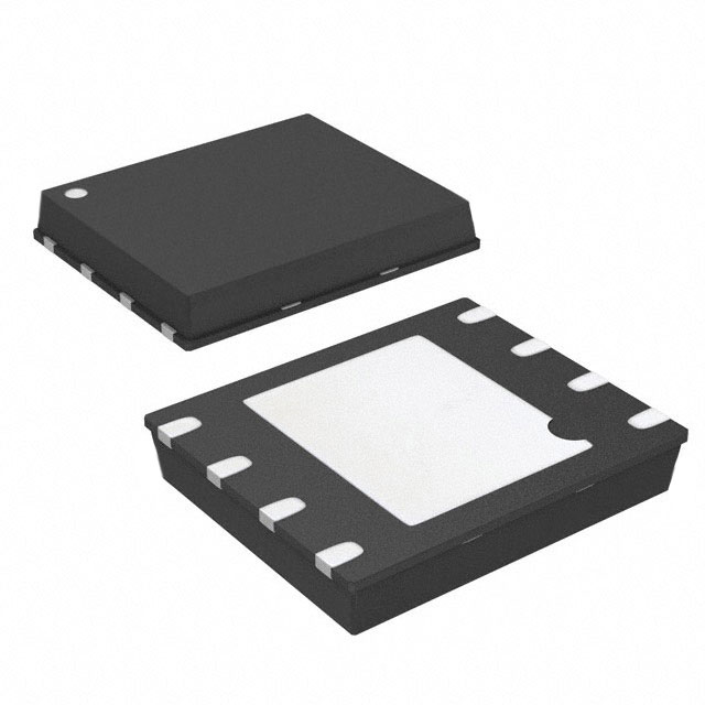


 工商网监
湘ICP备2023018690号
工商网监
湘ICP备2023018690号
