Data Sheet
BCR12FM-12LB
600V - 12A - Triac
R07DS1104EJ0202
Rev.2.02
Feb. 19, 2019
Medium Power Use
Features
•
•
•
•
• Insulated Type
• Planar Passivation Type
• Viso: 2000V
IT (RMS) : 12 A
VDRM : 600 V
Tj: 150 °C
IFGTI, IRGTI, IRGT III: 30 mA(20mA) Note5
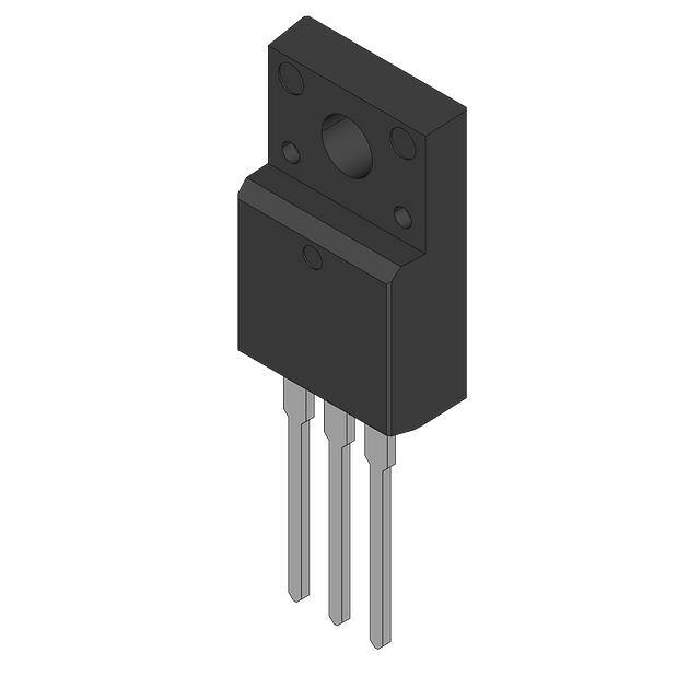
Outline
RENESAS Package code: PRSS0003AG-A
(Package name: TO-220FP)
RENESAS Package code: PRSS0003AP-A
(Package name: TO-220FPA)
Ordering code
#BB0
Ordering code
#BG0
#BH0
2
3
1. T1 Terminal
2. T2 Terminal
3. Gate Terminal
1
1
1 2
3
2 3
Application
Motor control, Heater control, Power supply, Solid state relay, and other general purpose AC control applications.
Maximum Ratings
Parameter
Symbol
Voltage class
Unit
Repetitive peak off-state voltageNote1
VDRM
12
600
V
Non-repetitive peak off-state voltageNote1
VDSM
720
V
Symbol
Ratings
Unit
Conditions
RMS on-state current
Parameter
IT (RMS)
12
A
Surge on-state current
ITSM
120
A
I2 t
60
A2s
Commercial frequency, sine full wave
360conduction,
Tc = 102C (#BB0, #BH0) Note2
Tc = 93C (#BG0) Note2
50 Hz sinewave 1 full cycle, peak value,
non-repetitive
Value corresponding to 1 cycle of half wave
50 Hz, surge on-state current
PGM
5
W
PG (AV)
VGM
0.5
10
W
V
Peak gate current
Junction Temperature
IGM
Tj
2
–40 to +150
A
C
Storage temperature
Isolation voltage Note7
Tstg
Viso
–40 to +150
2000
C
V
I2t for fusion
Peak gate power dissipation
Average gate power dissipation
Peak gate voltage
Ta=25C, AC 1 minute,
T1 • T2 • G terminal to case
Notes: 1. Gate open.
2. Please refer to the Ordering Information.
R07DS1104EJ0202 Rev.2.02
Feb. 19, 2019
Page 1 of 8
�BCR12FM-12LB
Data Sheet
Electrical Characteristics
Parameter
Repetitive peak off-state current
On-state voltage
Gate trigger voltageNote3
Gate trigger curentNote3
Symbol
IDRM
VTM
Min.
—
—
Typ.
—
—
Max.
2.0
1.6
Unit
mA
V
VFGT
VRGT
—
—
—
—
1.5
1.5
V
V
VRGT
—
—
1.5
V
IFGT
—
—
30 Note6
mA
mA
mA
Gate non-trigger voltage
Thermal resistance
Critical-rate of rise of off-state
commutation voltageNote5
Notes: 3.
4.
5.
6.
7.
IRGT
IRGT
—
—
—
—
30 Note6
VGD
0.2
0.1
—
—
—
—
V
Rth (j-c)
—
—
3.3
C/W
—
—
4.0
C/W
10
1
—
—
—
—
V/s
(dv/dt)c
30 Note6
Test conditions
Tj = 150C, VDRM applied
Tc = 25C, ITM = 20 A,
instantaneous measurement
Tj = 25C, VD = 6 V, RL = 6 ,
RG = 330
Tj = 25C, VD = 6 V, RL = 6 ,
RG = 330
Tj = 125C, VD = 1/2 VDRM
Tj = 150C, VD = 1/2 VDRM
Junction to caseNote4
(#BB0, #BH0) Note2
Junction to caseNote4
(#BG0) Note2
Tj = 125C
Tj = 150C
Measurement using the gate trigger characteristics measurement circuit.
The contact thermal resistance Rth(c-f) in case of greasing is 0.5C/W.
Test conditions of the critical-rate of rise of off-state commutation voltage is shown in the table below.
High sensitivity (IGT 20 mA) is also available. (IGT item:1)
Make sure that your finished product containing this device meets your safe isolation requirements.
For safety, it's advisable that heatsink is electrically floating.
Test conditions
1. Junction temperature
Tj = 125°C/150°C
Commutating voltage and current waveforms
(inductive load)
Supply Voltage
Time
2. Rate of decay of on-state commutating current
(di/dt)c = – 6 A/ms
Main Current
(di/dt)c
Time
3. Peak off-state voltage
VD = 400 V
Main Voltage
(dv/dt)c
R07DS1104EJ0202 Rev.2.02
Feb. 19, 2019
Time
VD
Page 2 of 8
�BCR12FM-12LB
Data Sheet
Performance Curves
Maximum On-State Characteristics
Rated Surge On-State Current
Surge On-State Current (A)
200
Tj = 150°C
101
Tj = 25°C
100
0
1
2
3
120
100
80
60
40
20
101
102
Gate Characteristics (I, II and III)
Gate Trigger Current vs.
Junction Temperature
PG(AV) = 0.5W
PGM = 5W
IGM = 2A
VGT = 1.5V
100
IFGT I IRGT I, IRGT III
101
102
VGD = 0.1V
103
104
103
Typical Example
IRGT I
102
IFGT I
IRGT III
101
- 40
0
40
80
120
160
Gate Current (mA)
Junction Temperature (°C)
Gate Trigger Voltage vs.
Junction Temperature
Gate Trigger Current vs.
Gate Current Pulse Width
103
Typical Example
102
101
- 40
Gate Trigger Current (Tj = t°C)
× 100 (%)
Gate Trigger Current (Tj = 25°C)
Gate Voltage (V)
140
Conduction Time (Cycles at 60Hz)
101
Gate Trigger Voltage (Tj = t°C)
× 100 (%)
Gate Trigger Voltage (Tj = 25°C)
160
On-State Voltage (V)
VGM = 10V
10- 1
180
0
100
4
0
40
80
120
Junction Temperature (°C)
R07DS1104EJ0202 Rev.2.02
Feb. 19, 2019
160
Gate Trigger Current (tw)
× 100 (%)
Gate Trigger Current (DC)
On-State Current (A)
102
103
Typical Example
IFGT I
IRGT I
IRGT III
102
101
100
101
102
Gate Current Pulse Width (s)
Page 3 of 8
�BCR12FM-12LB
Data Sheet
5
103
#BB0,#BH0
#BG0
4
3
2
1
0 -1
10
100
101
102
103
No Fins
102
101
100
10- 1
101
102
103
104
105
Conduction Time (Cycles at 60Hz)
Conduction Time (Cycles at 60Hz)
Maximum On-State Power Dissipation
Allowable Case Temperature vs.
RMS On-State Current
160
14
140
Case Temperature (°C)
16
12 360° Conduction
Resistive,
10 inductive loads
8
6
4
2
0
0
2
4
6
8
10
12
14
16
Curves apply regardless
of conduction angle
120
100
#BB0,#BH0
#BG0
80
60
40
360° Conduction
20 Resistive,
inductive loads
0
0
2
4
6
8
10
12
14
16
RMS On-State Current (A)
RMS On-State Current (A)
Allowable Ambient Temperature vs.
RMS On-State Current
Allowable Ambient Temperature vs.
RMS On-State Current
160
Ambient Temperature (°C)
104
Transient Thermal Impedance (°C/W)
102
6
Maximum Transient Thermal Impedance
Characteristics (Junction to ambient)
120
All fins are black painted
aluminum and greased
#BB0,#BH0
#BG0
100
100 ×100 ×t2.3
80
60 ×60 ×t2.3
140
60 Curves apply
regardless of
40 conduction angle
Resistive,
20 inductive loads
Natural convection
0
0
2
4
6
8
10
12
14
RMS On-State Current (A)
R07DS1104EJ0202 Rev.2.02
Feb. 19, 2019
16
160
Ambient Temperature (°C)
On-State Power Dissipation (W)
Transient Thermal Impedance (°C/W)
Maximum Transient Thermal Impedance
Characteristics (Junction to case)
Natural convection
No Fins
Curves apply regardless
of conduction angle
Resistive, inductive loads
140
120
100
80
60
40
20
0
0
0.5 1.0 1.5 2.0 2.5 3.0 3.5 4.0
RMS On-State Current (A)
Page 4 of 8
�BCR12FM-12LB
Data Sheet
Latching Current vs.
Junction Temperature
Holding Current vs.
Junction Temperature
103
Typical Distribution
Typical Distribution
III Quadrant
Typical Example
101
I Quadrant
Typical Example
VD=12V
100
- 40
0
40
80
120
Latching Current (mA)
Holding Current (mA)
102
T2+,G Typical Example
102
101
T2+,G+ T2- ,GTypical Example
100
- 40
160
140
120
100
80
60
40
20
0
40
80
120
160
Breakover Voltage (dv/dt = xV/s)
× 100 (%)
Breakover Voltage (dv/dt = 1V/s)
Junction Temperature (°C)
Breakover Voltage vs.
Rate of Rise of Off-State Voltage (Tj=125°C)
160
Typical Example
Tj = 125°C
140
120
III Quadrant
100
80
60
I Quadrant
40
20
0 1
10
102
103
104
Rate of Rise of Off-State Voltage (V/s)
R07DS1104EJ0202 Rev.2.02
Feb. 19, 2019
Repetitive Peak Off-State Current (Tj = t°C)
×100 (%)
Repetitive Peak Off-State Current (Tj = 25°C)
Typical Example
Breakover Voltage (dv/dt = xV/s)
× 100 (%)
Breakover Voltage (dv/dt = 1V/s)
Breakover Voltage (Tj = t°C)
× 100 (%)
Breakover Voltage (Tj = 25°C)
Breakover Voltage vs.
Junction Temperature
0
- 40
40
80
120
160
Junction Temperature (°C)
Junction Temperature (°C)
160
0
Repetitive Peak Off-State Current vs.
Junction Temperature
106
Typical Example
105
104
103
102
- 40
0
40
80
120
160
Junction Temperature (°C)
Breakover Voltage vs.
Rate of Rise of Off-State Voltage (Tj=150°C)
160
Typical Example
Tj = 150°C
140
120
III Quadrant
100
80
60
I Quadrant
40
20
0 1
10
102
103
104
Rate of Rise of Off-State Voltage (V/s)
Page 5 of 8
�BCR12FM-12LB
Data Sheet
Commutation Characteristics (Tj=125°C)
Typical Example
Tj = 125°C
IT = 4 A
t = 500 s
VD = 200 V
f = 3 Hz
101
Main Voltage
(dv/dt)c
Main Current
IT
102
Time
Critical Rate of Rise of Off-State
Commutating Voltage (V/s)
Critical Rate of Rise of Off-State
Commutating Voltage (V/s)
102
Commutation Characteristics (Tj=150°C)
VD
(di/dt)c
t
Time
Minimum
Value
I Quadrant
III Quadrant
100
100
101
102
Rate of Decay of On-State
Commutating Current (A/ms)
Main Current
IT
Time
VD
(di/dt)c
t
Time
Typical Example
Tj = 150°C
IT = 4 A
t = 500 s
VD = 200 V
f = 3 Hz
101
I Quadrant
III Quadrant
100
100
Minimum
Value
101
102
Rate of Decay of On-State
Commutating Current (A/ms)
Gate Trigger Characteristics Test Circuits
6
Main Voltage
(dv/dt)c
6
Recommended peripheral components for Triac
Load
C1
A
6V
330
V
Test Procedure I
A
6V
V
330
Test Procedure II
R1
C0
R0
C1 = 0.1 to 0.47 F C0 = 0.1 F
R1 = 47 to 100
R0 = 100
6
A
6V
V
330
Test Procedure III
R07DS1104EJ0202 Rev.2.02
Feb. 19, 2019
Page 6 of 8
�BCR12FM-12LB
Data Sheet
Package Dimensions
Ordering code: #BG0, #BH0
JEITA Package Code
-
RENESAS Code
Previous Code
MASS (Typ) [g]
PRSS0003AP-A
TO-220FPA
1.65
Unit: mm
2.7±0.2
f 3.2±0.2
1.95±0.3
15.0±0.3
6.9±0.3
10.0±0.3
0.745±0.2
13.0±0.5
0.395±0.2
1.14±0.2
0.69±0.15
0.60 +0.19
- 0.11
2.54±0.25
3.2±0.2
4.5±0.2
2.54±0.25
R07DS1104EJ0202 Rev.2.02
Feb. 19, 2019
Page 7 of 8
�BCR12FM-12LB
Data Sheet
Package Dimensions
Ordering code: #BB0
Package Name
TO-220FP
JEITA Package Code
RENESAS Code
PRSS0003AG-A
MASS[Typ.]
1.9g
Previous Code
10.16±0.20
2.54±0.20
6.68 ±0.20
3.3±0.2
1.28 ±0.30
3.18 ±0.20
15.87±0.20
f 3.18±0.10
12.98 ±0.30
Unit: mm
Max 1.47
2.76 ±0.20
0.80±0.20
0.50
4.7±0.2
5.08 ±0.20
Ordering Information
Orderable Part Number
BCR12FM-12LB#BG0
Package
TO-220FPA
Quantity Note8
Remark
50 pcs./ tube Straight type
BCR12FM-12LB-1#BG0
BCR12FM-12LB#BG0
TO-220FPA
TO-220FPA
50 pcs./ tube
50 pcs./ tube
Straight type, IGT item:1
:Lead form type
BCR12FM12LB1#BG0
BCR12FM-12LB#BH0
TO-220FPA
TO-220FPA
50 pcs./ tube
50 pcs./ tube
:Lead form type, IGT item:1
Straight type
BCR12FM-12LB-1#BH0
BCR12FM-12LB#BH0
TO-220FPA
TO-220FPA
50 pcs./ tube
50 pcs./ tube
Straight type, IGT item:1
:Lead form type
BCR12FM12LB1#BH0
BCR12FM-12LB#BB0
TO-220FPA
TO-220FP
50 pcs./ tube
50 pcs./ tube
:Lead form type, IGT item:1
Straight type
EOL announced
BCR12FM-12LB#BB0
TO-220FP
50 pcs./ tube
:Lead form type
Status
Mass Production
Notes: 8. Please confirm the specification about the shipping in detail.
R07DS1104EJ0202 Rev.2.02
Feb. 19, 2019
Page 8 of 8
�Notice
1.
Descriptions of circuits, software and other related information in this document are provided only to illustrate the operation of semiconductor products and application examples. You are fully responsible for
the incorporation or any other use of the circuits, software, and information in the design of your product or system. Renesas Electronics disclaims any and all liability for any losses and damages incurred by
you or third parties arising from the use of these circuits, software, or information.
2.
Renesas Electronics hereby expressly disclaims any warranties against and liability for infringement or any other claims involving patents, copyrights, or other intellectual property rights of third parties, by or
arising from the use of Renesas Electronics products or technical information described in this document, including but not limited to, the product data, drawings, charts, programs, algorithms, and application
examples.
3.
No license, express, implied or otherwise, is granted hereby under any patents, copyrights or other intellectual property rights of Renesas Electronics or others.
4.
You shall not alter, modify, copy, or reverse engineer any Renesas Electronics product, whether in whole or in part. Renesas Electronics disclaims any and all liability for any losses or damages incurred by
5.
Renesas Electronics products are classified according to the following two quality grades: “Standard” and “High Quality”. The intended applications for each Renesas Electronics product depends on the
you or third parties arising from such alteration, modification, copying or reverse engineering.
product’s quality grade, as indicated below.
"Standard":
Computers; office equipment; communications equipment; test and measurement equipment; audio and visual equipment; home electronic appliances; machine tools; personal electronic
equipment; industrial robots; etc.
"High Quality": Transportation equipment (automobiles, trains, ships, etc.); traffic control (traffic lights); large-scale communication equipment; key financial terminal systems; safety control equipment; etc.
Unless expressly designated as a high reliability product or a product for harsh environments in a Renesas Electronics data sheet or other Renesas Electronics document, Renesas Electronics products are
not intended or authorized for use in products or systems that may pose a direct threat to human life or bodily injury (artificial life support devices or systems; surgical implantations; etc.), or may cause
serious property damage (space system; undersea repeaters; nuclear power control systems; aircraft control systems; key plant systems; military equipment; etc.). Renesas Electronics disclaims any and all
liability for any damages or losses incurred by you or any third parties arising from the use of any Renesas Electronics product that is inconsistent with any Renesas Electronics data sheet, user’s manual or
other Renesas Electronics document.
6.
When using Renesas Electronics products, refer to the latest product information (data sheets, user’s manuals, application notes, “General Notes for Handling and Using Semiconductor Devices” in the
reliability handbook, etc.), and ensure that usage conditions are within the ranges specified by Renesas Electronics with respect to maximum ratings, operating power supply voltage range, heat dissipation
characteristics, installation, etc. Renesas Electronics disclaims any and all liability for any malfunctions, failure or accident arising out of the use of Renesas Electronics products outside of such specified
ranges.
7.
Although Renesas Electronics endeavors to improve the quality and reliability of Renesas Electronics products, semiconductor products have specific characteristics, such as the occurrence of failure at a
certain rate and malfunctions under certain use conditions. Unless designated as a high reliability product or a product for harsh environments in a Renesas Electronics data sheet or other Renesas
Electronics document, Renesas Electronics products are not subject to radiation resistance design. You are responsible for implementing safety measures to guard against the possibility of bodily injury, injury
or damage caused by fire, and/or danger to the public in the event of a failure or malfunction of Renesas Electronics products, such as safety design for hardware and software, including but not limited to
redundancy, fire control and malfunction prevention, appropriate treatment for aging degradation or any other appropriate measures. Because the evaluation of microcomputer software alone is very difficult
and impractical, you are responsible for evaluating the safety of the final products or systems manufactured by you.
8.
Please contact a Renesas Electronics sales office for details as to environmental matters such as the environmental compatibility of each Renesas Electronics product. You are responsible for carefully and
sufficiently investigating applicable laws and regulations that regulate the inclusion or use of controlled substances, including without limitation, the EU RoHS Directive, and using Renesas Electronics
products in compliance with all these applicable laws and regulations. Renesas Electronics disclaims any and all liability for damages or losses occurring as a result of your noncompliance with applicable
laws and regulations.
9.
Renesas Electronics products and technologies shall not be used for or incorporated into any products or systems whose manufacture, use, or sale is prohibited under any applicable domestic or foreign laws
or regulations. You shall comply with any applicable export control laws and regulations promulgated and administered by the governments of any countries asserting jurisdiction over the parties or
transactions.
10. It is the responsibility of the buyer or distributor of Renesas Electronics products, or any other party who distributes, disposes of, or otherwise sells or transfers the product to a third party, to notify such third
party in advance of the contents and conditions set forth in this document.
11. This document shall not be reprinted, reproduced or duplicated in any form, in whole or in part, without prior written consent of Renesas Electronics.
12. Please contact a Renesas Electronics sales office if you have any questions regarding the information contained in this document or Renesas Electronics products.
(Note 1)
“Renesas Electronics” as used in this document means Renesas Electronics Corporation and also includes its directly or indirectly controlled subsidiaries.
(Note 2)
“Renesas Electronics product(s)” means any product developed or manufactured by or for Renesas Electronics.
(Rev.4.0-1 November 2017)
http://www.renesas.com
SALES OFFICES
Refer to "http://www.renesas.com/" for the latest and detailed information.
Renesas Electronics Corporation
TOYOSU FORESIA, 3-2-24 Toyosu, Koto-ku, Tokyo 135-0061, Japan
Renesas Electronics America Inc.
1001 Murphy Ranch Road, Milpitas, CA 95035, U.S.A.
Tel: +1-408-432-8888, Fax: +1-408-434-5351
Renesas Electronics Canada Limited
9251 Yonge Street, Suite 8309 Richmond Hill, Ontario Canada L4C 9T3
Tel: +1-905-237-2004
Renesas Electronics Europe Limited
Dukes Meadow, Millboard Road, Bourne End, Buckinghamshire, SL8 5FH, U.K
Tel: +44-1628-651-700
Renesas Electronics Europe GmbH
Arcadiastrasse 10, 40472 Düsseldorf, Germany
Tel: +49-211-6503-0, Fax: +49-211-6503-1327
Renesas Electronics (China) Co., Ltd.
Room 1709 Quantum Plaza, No.27 ZhichunLu, Haidian District, Beijing, 100191 P. R. China
Tel: +86-10-8235-1155, Fax: +86-10-8235-7679
Renesas Electronics (Shanghai) Co., Ltd.
Unit 301, Tower A, Central Towers, 555 Langao Road, Putuo District, Shanghai, 200333 P. R. China
Tel: +86-21-2226-0888, Fax: +86-21-2226-0999
Renesas Electronics Hong Kong Limited
Unit 1601-1611, 16/F., Tower 2, Grand Century Place, 193 Prince Edward Road West, Mongkok, Kowloon, Hong Kong
Tel: +852-2265-6688, Fax: +852 2886-9022
Renesas Electronics Taiwan Co., Ltd.
13F, No. 363, Fu Shing North Road, Taipei 10543, Taiwan
Tel: +886-2-8175-9600, Fax: +886 2-8175-9670
Renesas Electronics Singapore Pte. Ltd.
80 Bendemeer Road, Unit #06-02 Hyflux Innovation Centre, Singapore 339949
Tel: +65-6213-0200, Fax: +65-6213-0300
Renesas Electronics Malaysia Sdn.Bhd.
Unit 1207, Block B, Menara Amcorp, Amcorp Trade Centre, No. 18, Jln Persiaran Barat, 46050 Petaling Jaya, Selangor Darul Ehsan, Malaysia
Tel: +60-3-7955-9390, Fax: +60-3-7955-9510
Renesas Electronics India Pvt. Ltd.
No.777C, 100 Feet Road, HAL 2nd Stage, Indiranagar, Bangalore 560 038, India
Tel: +91-80-67208700, Fax: +91-80-67208777
Renesas Electronics Korea Co., Ltd.
17F, KAMCO Yangjae Tower, 262, Gangnam-daero, Gangnam-gu, Seoul, 06265 Korea
Tel: +82-2-558-3737, Fax: +82-2-558-5338
© 2019 Renesas Electronics Corporation. All rights reserved.
Colophon 7.2
�