DATASHEET
CA3420
FN1320
Rev 9.00
Oct 4, 2005
0.5MHz, Low Supply Voltage, Low Input Current BiMOS Operational Amplifier
The CA3420 is an integrated circuit operational amplifier that
combines PMOS transistors and bipolar transistors on a
single monolithic chip. The CA3420 BiMOS operational
amplifier features gate protected PMOS transistors in the
input circuit to provide very high input impedance, very low
input currents (less than 1pA). The internal bootstrapping
network features a unique guardbanding technique for
reducing the doubling of leakage current for every 10°C
increase in temperature. The CA3420 operates at total
supply voltages from 2V to 20V either single or dual supply.
This operational amplifier is internally phase compensated to
achieve stable operation in the unity gain follower
configuration. Additionally, it has access terminals for a
supplementary external capacitor if additional frequency rolloff is desired. Terminals are also provided for use in
applications requiring input offset voltage nulling. The use of
PMOS in the input stage results in common mode input
voltage capability down to 0.45V below the negative supply
terminal, an important attribute for single supply application.
The output stage uses a feedback OTA type amplifier that
can swing essentially from rail-to-rail. The output driving
current of 1.5mA (Min) is provided by using nonlinear current
mirrors.
Features
• 2V Supply at 300A Supply Current
• 1pA Input Current (Typ) (Essentially Constant to 85°C)
• Rail-to-Rail Output Swing (Drive 2mA into 1k Load)
• Pin Compatible with 741 Operational Amplifiers
• Pb-Free Plus Anneal Available (RoHS Compliant)
Applications
• pH Probe Amplifiers
• Picoammeters
• Electrometer (High Z) Instruments
• Portable Equipment
• Inaccessible Field Equipment
• Battery-Dependent Equipment (Medical and Military)
Functional Diagram
X1
Ordering Information
PART
NUMBER
PART
MARKING
TEMP.
RANGE (°C)
PACKAGE
PKG.
DWG. #
CA3420E
CA3420E
-55 to 125
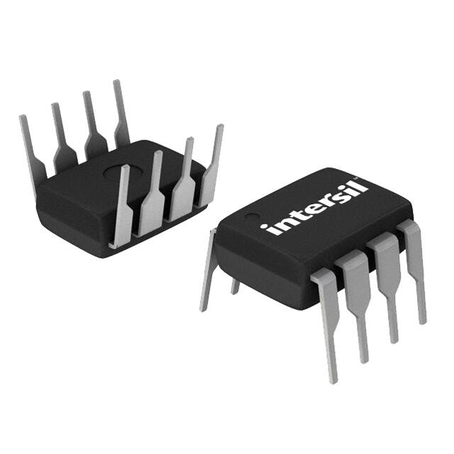
8 Ld PDIP
E8.3
CA3420EZ
(Note)
CA3420EZ
-55 to 125
8 Ld PDIP*
(Pb-free)
E8.3
MOS
BIPOLAR
*Pb-free PDIPs can be used for through hole wave solder
processing only. They are not intended for use in Reflow solder
processing applications.
NOTE: Intersil Pb-free plus anneal products employ special
Pb-free material sets; molding compounds/die attach materials and
100% matte tin plate termination finish, which are RoHS compliant
and compatible with both SnPb and Pb-free soldering operations.
Intersil Pb-free products are MSL classified at Pb-free peak reflow
temperatures that meet or exceed the Pb-free requirements of
IPC/JEDEC J STD-020.
+
MOS
BIPOLAR
HIGH GAIN
(50K)
OTA BUFFER
(X2)
X1
BUFFER AMPS;
BOOTSTRAPPED
INPUT PROTECTION
NETWORK
Pinout
CA3420 (PDIP)
TOP VIEW
FN1320 Rev 9.00
Oct 4, 2005
OFFSET NULL
1
INV.
INPUT
2
NON-INV.
INPUT
3
V-
4
8 STROBE
+
7 V+
6 OUTPUT
5 OFFSET NULL
Page 1 of 5
�CA3420
Absolute Maximum Ratings
Thermal Information
Supply Voltage (V+ to V-). . . . . . . . . . . . . . . . . . . . . . . . . . . . . . .22V
Differential Input Voltage . . . . . . . . . . . . . . . . . . . . . . . . . . . . . . .15V
DC Input Voltage . . . . . . . . . . . . . . . . . . . . . . (V+ + 8V) to (V- -0.5V)
Input Current . . . . . . . . . . . . . . . . . . . . . . . . . . . . . . . . . . . . . . . 1mA
Output Short Circuit Duration (Note 1). . . . . . . . . . . . . . . . Indefinite
Thermal Resistance (Typical, Note 2)
Operating Conditions
Temperature Range . . . . . . . . . . . . . . . . . . . . . . . . . -55°C to 125°C
JA (°C/W)
JC (°C/W)
PDIP Package* . . . . . . . . . . . . . . . . . .
105
N/A
Maximum Junction Temperature (Plastic Package) . . . . . . . 150°C
Maximum Storage Temperature Range . . . . . . . . . . -65°C to 150°C
Maximum Lead Temperature (Soldering 10s) . . . . . . . . . . . . 300°C
*Pb-free PDIPs can be used for through hole wave solder processing
only. They are not intended for use in Reflow solder processing
applications.
CAUTION: Stresses above those listed in “Absolute Maximum Ratings” may cause permanent damage to the device. This is a stress only rating and operation of the
device at these or any other conditions above those indicated in the operational sections of this specification is not implied.
NOTES:
1. Short circuit may be applied to ground or to either supply.
2. JA is measured with the component mounted on an evaluation PC board in free air.
Electrical Specifications
Typical Values Intended Only for Design Guidance, VSUPPLY = 10V, TA = 25°C
PARAMETER
SYMBOL
Input Resistance
TEST CONDITIONS
RI
TYP
UNITS
150
T
Input Capacitance
CI
4.9
pF
Output Resistance
RO
300
Equivalent Input Noise Voltage
eN
f = 1kHz
RS = 100
f = 10kHz
Short-Circuit Current
Source
IOM+
To Opposite Supply
Sink
62
nV/Hz
38
nV/Hz
2.6
mA
IOM-
2.4
mA
Gain Bandwidth Product
fT
0.5
MHz
Slew Rate
SR
0.5
V/s
Transient Response
Current from Terminal 8
Electrical Specifications
Rise Time
tR
0.7
s
Overshoot
OS
15
%
To V-
I8+
20
A
To V+
I8-
2
mA
RL = 2k, CL = 100pF
For Equipment Design, At VSUPPLY = 1V, TA = 25°C, Unless Otherwise Specified
PARAMETER
SYMBOL
TEST
CONDITIONS
MIN
TYP
MAX
UNITS
mV
|VIO|
-
5
10
Input Offset Current (Note 3)
|IIO|
-
0.01
4
pA
Input Current (Note 3)
|II|
-
1
5
pA
10
100
-
kV/V
Input Offset Voltage
Large Signal Voltage Gain
AOL
RL = 10k
80
100
-
dB
Common Mode Rejection Ratio
CMRR
-
560
1800
V/V
55
65
-
dB
Common Mode Input Voltage Range
VlCR+
0.2
0.5
-
V
-
-1.3
-
V
Power Supply Rejection Ratio
PSRR
VIO/V
-
100
1000
V/V
60
80
-
dB
Max Output Voltage
VOM+
RL =
0.90
0.95
-
V
VOM-
-0.85
-0.91
-
V
I+
-
350
650
A
PD
-
0.7
1.1
mW
VlO/T
-
4
-
V/°C
VlCR-
Supply Current
Device Dissipation
Input Offset Voltage Temperature Drift
NOTE:
3. The maximum limit represents the levels obtainable on high speed automatic test equipment. Typical values are obtained under laboratory conditions.
FN1320 Rev 9.00
Oct 4, 2005
Page 2 of 5
�CA3420
Electrical Specifications
For Equipment Design, at VSUPPLY = 10V, TA = 25°C, Unless Otherwise Specified
PARAMETER
TEST
CONDITIONS
MIN
TYP
MAX
UNITS
|VIO|
-
5
10
mV
Input Offset Current (Note 4)
|IIO|
-
0.03
4
pA
Input Current (Note 4)
|II|
-
0.05
5
pA
kV/V
Input Offset Voltage
Large Signal Voltage Gain
Common Mode Rejection Ratio
Common Mode Input Voltage Range
Power Supply Rejection Ratio
Max Output Voltage
SYMBOL
AOL
CMRR
10
100
-
80
100
-
dB
-
100
320
V/V
70
80
-
dB
VlCR+
8.5
9.3
-
V
VlCR-
-10
-10.3
-
V
VIO/V
-
32
320
V/V
70
90
-
dB
9.7
9.9
-
V
VOM-
-9.7
-9.85
-
V
I+
-
450
1000
A
PD
-
9
14
mW
VlO/T
-
4
-
V/°C
PSRR
VOM+
Supply Current
Device Dissipation
Input Offset Voltage Temperature Drift
RL = 10k
RL =
NOTE:
4. The maximum limit represents the levels obtainable on high speed automatic test equipment. Typical values are obtained under laboratory conditions.
Typical Applications
10G
10pF
+1.5V
Picoammeter Circuit
The exceptionally low input current (typically 0.2pA) makes
the CA3420 highly suited for use in a picoammeter circuit.
With only a single 10G resistor, this circuit covers the range
from 1.5pA. Higher current ranges are possible with suitable
switching techniques and current scaling resistors. Input
transient protection is provided by the 1M resistor in series
with the input. Higher current ranges require that this resistor
be reduced. The 10M resistor connected to pin 2 of the
CA3420 decouples the potentially high input capacitance
often associated with lower current circuits and reduces the
tendency for the circuit to oscillate under these conditions.
2
1M
The meter is placed in series with the gain network, thus
eliminating the meter temperature coefficient error term.
Supply current in the standby position with the meter
undeflected is 300A. At full-scale deflection this current
rises to 800A. Carbon-zinc battery life should be in excess
of 1,000 hours.
500-0-500
A
7
-
6
CA3420
3
+
1
M
50pA
4
5
BATTERY
RETURNS
15pA
1.5k
1.5k, 1%
1k
10k
5pA
-1.5V
1.5pA
11k
High Input Resistance Voltmeter
Advantage is taken of the high input impedance of the CA3420
in a high input resistance DC voltmeter. Only two 1.5V “AA”
type penlite batteries power this exceedingly high-input
resistance (>1,000,000M) DC voltmeter. Full-scale deflection
is 500mV, 150mV, and 15mV. Higher voltage ranges are
easily added with external input voltage attenuator networks.
10M
430, 1%
150, 1%
68
1%
FIGURE 1. PICOAMMETER CIRCUIT
+1.5V
3
22M
10M
100pF
+
6
CA3420
2
1
500-0-500
A
7
5
M
500mV
4
BATTERY
RETURNS
10k
150mV
1.5k
1.5k, 1%
1k
50mV
430, 1%
-1.5V
15mV
1.1k
150, 1%
68
1%
FIGURE 2. HIGH INPUT RESISTANCE VOLTMETER
FN1320 Rev 9.00
Oct 4, 2005
Page 3 of 5
�CA3420
1.0
OUTPUT STAGE TRANSISTOR SATURATION
VOLTAGE, Q19 (mV)
INPUT & OUTPUT VOLTAGE EXCURSIONS FROM THE
POSITIVE AND NEGATIVE SUPPLY VOLTAGE (V)
Typical Performance Curves
TA = 25°C
RL = 100k
0.8
0.6
0.4
0.2
V O-
0
-0.2
VO+
-0.4
VICR-
-0.6
VICR+
-0.8
1
10
5
TA = 25°C
V- = 0V
V+ = 2V
V+ = 5V
V+ = 10V
V+ = 20V
100
1000
0.01
-1.0
0
10
15
0.1
SUPPLY VOLTAGE (V)
TA = 25°C
V+ = 0V
V- = -20V
V- = -10V
V- = -5V
V- = -2V
100
10
0.01
0.1
1
10
1000
TA = 25°C
VS = 10V
VS = 5V
VS = 1V
100
10
1
101
102
103
LOAD (SINKING) CURRENT (mA)
104
105
106
FREQUENCY (Hz)
FIGURE 6. INPUT NOISE VOLTAGE vs FREQUENCY
TA = 25°C
VS = 5V
RL = 10k
CL = 0pF
100
0
-45
80
-90
60
-135
-180
40
OPEN LOOP PHASE (DEGREES)
FIGURE 5. OUTPUT VOLTAGE vs LOAD SINKING CURRENT
OPEN LOOP VOLTAGE GAIN (dB)
10
FIGURE 4. OUTPUT VOLTAGE vs LOAD SOURCING CURRENT
EQUIVALENT INPUT NOISE VOLTAGE (nV/Hz)
OUTPUT STAGE TRANSISTOR SATURATION
VOLTAGE, Q17 (mV)
FIGURE 3. OUTPUT VOLTAGE SWING AND COMMON MODE
INPUT VOLTAGE RANGE vs SUPPLY VOLTAGE
1000
1
LOAD (SOURCING) CURRENT (mA)
20
0
1
101
102
103
104
105
106
FREQUENCY (Hz)
FIGURE 7. OPEN LOOP GAIN AND PHASE SHIFT RESPONSE
FN1320 Rev 9.00
Oct 4, 2005
Page 4 of 5
�CA3420
Dual-In-Line Plastic Packages (PDIP)
E8.3 (JEDEC MS-001-BA ISSUE D)
N
8 LEAD DUAL-IN-LINE PLASTIC PACKAGE
E1
INDEX
AREA
1 2 3
INCHES
N/2
-B-
-AD
E
BASE
PLANE
-C-
SEATING
PLANE
A2
A
L
D1
e
B1
D1
A1
eC
B
0.010 (0.25) M
C A B S
MILLIMETERS
SYMBOL
MIN
MAX
MIN
MAX
NOTES
A
-
0.210
-
5.33
4
A1
0.015
-
0.39
-
4
A2
0.115
0.195
2.93
4.95
-
B
0.014
0.022
0.356
0.558
-
C
L
B1
0.045
0.070
1.15
1.77
8, 10
eA
C
0.008
0.014
0.204
C
D
0.355
0.400
9.01
eB
NOTES:
1. Controlling Dimensions: INCH. In case of conflict between
English and Metric dimensions, the inch dimensions control.
5
D1
0.005
-
0.13
-
5
E
0.300
0.325
7.62
8.25
6
E1
0.240
0.280
6.10
7.11
5
e
0.100 BSC
2. Dimensioning and tolerancing per ANSI Y14.5M-1982.
eA
0.300 BSC
3. Symbols are defined in the “MO Series Symbol List” in Section
2.2 of Publication No. 95.
eB
-
L
0.115
4. Dimensions A, A1 and L are measured with the package seated
in JEDEC seating plane gauge GS-3.
0.355
10.16
N
2.54 BSC
7.62 BSC
0.430
-
0.150
2.93
8
5. D, D1, and E1 dimensions do not include mold flash or protrusions. Mold flash or protrusions shall not exceed 0.010 inch
(0.25mm).
6. E and eA are measured with the leads constrained to be perpendicular to datum -C- .
8
6
10.92
7
3.81
4
9
Rev. 0 12/93
7. eB and eC are measured at the lead tips with the leads unconstrained. eC must be zero or greater.
8. B1 maximum dimensions do not include dambar protrusions.
Dambar protrusions shall not exceed 0.010 inch (0.25mm).
9. N is the maximum number of terminal positions.
10. Corner leads (1, N, N/2 and N/2 + 1) for E8.3, E16.3, E18.3,
E28.3, E42.6 will have a B1 dimension of 0.030 - 0.045 inch
(0.76 - 1.14mm).
© Copyright Intersil Americas LLC 2000-2005. All Rights Reserved.
All trademarks and registered trademarks are the property of their respective owners.
For additional products, see www.intersil.com/en/products.html
Intersil products are manufactured, assembled and tested utilizing ISO9001 quality systems as noted
in the quality certifications found at www.intersil.com/en/support/qualandreliability.html
Intersil products are sold by description only. Intersil may modify the circuit design and/or specifications of products at any time without notice, provided that such
modification does not, in Intersil's sole judgment, affect the form, fit or function of the product. Accordingly, the reader is cautioned to verify that datasheets are
current before placing orders. Information furnished by Intersil is believed to be accurate and reliable. However, no responsibility is assumed by Intersil or its
subsidiaries for its use; nor for any infringements of patents or other rights of third parties which may result from its use. No license is granted by implication or
otherwise under any patent or patent rights of Intersil or its subsidiaries.
For information regarding Intersil Corporation and its products, see www.intersil.com
FN1320 Rev 9.00
Oct 4, 2005
Page 5 of 5
�