CR04AM-12
Thyristor
Low Power Use
REJ03G0354-0200 Rev.2.00 Mar.01.2005
Features
• IT (AV) : 0.4 A • VDRM : 600 V • IGT : 100 µA • Glass Passivation Type
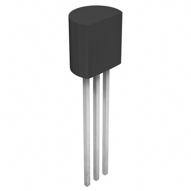
Outline
PRSS0003EA-A (Package name: TO-92)
2
3 1 3 2 1
1. Cathode 2. Anode 3. Gate
Applications
Igniter, solid state relay, strobe flasher, circuit breaker, and other general purpose control applications
Maximum Ratings
Parameter Repetitive peak reverse voltage Non-repetitive peak reverse voltage DC reverse voltage Repetitive peak off-state voltageNote1 DC off-state voltageNote1 Symbol VRRM VRSM VR (DC) VDRM VD (DC) Voltage class 12 600 720 480 600 480 Unit V V V V V
Rev.2.00,
Mar.01.2005,
page 1 of 7
�CR04AM-12
Parameter RMS on-state current Average on-state current Surge on-state current I2t for fusing Peak gate power dissipation Average gate power dissipation Peak gate forward voltage Peak gate reverse voltage Peak gate forward current Junction temperature Storage temperature Mass Symbol IT (RMS) IT (AV) ITSM I2 t PGM PG (AV) VFGM VRGM IFGM Tj Tstg — Ratings 0.63 0.4 10 0.4 0.5 0.1 6 6 0.3 – 40 to +125 – 40 to +125 0.23 Unit A A A A2s W W V V A °C °C g Conditions Commercial frequency, sine half wave 180° conduction, Ta = 54°C 60Hz sine half wave 1 full cycle, peak value, non-repetitive Value corresponding to 1 cycle of half wave 60Hz, surge on-state current
Typical value
Notes: 1. With gate to cathode resistance RGK = 1 kΩ.
Electrical Characteristics
Parameter Repetitive peak reverse current Repetitive peak off-state current On-state voltage Gate trigger voltage Gate non-trigger voltage Gate trigger current Holding current Thermal resistance Symbol IRRM IDRM VTM VGT VGD IGT IH Rth (j-a) Min. — — — — 0.2 1 — — Typ. — — — — — — 1.5 — Max. 0.5 0.5 1.2 0.8 — 100Note2 3 150 Unit mA mA V V V µA mA °C/W Test conditions Tj = 125°C, VRRM applied Tj = 125°C, VDRM applied, RGK = 1 kΩ Ta = 25°C, ITM = 1.2 A, instantaneous value Tj = 25°C, VD = 6 V, Note3 IT = 0.1 A Tj = 125°C, VD = 1/2 VDRM, RGK = 1 kΩ Tj = 25°C, VD = 6 V, Note3 IT = 0.1 A Tj = 25°C, VD = 12 V, RGK = 1 kΩ Junction to ambient
Notes: 2. If special values of IGT are required, choose item D or E from those listed in the table below if possible. Item A B C D E IGT (µA) 1 to 30 20 to 50 40 to 100 1 to 50 20 to 100 The above values do not include the current flowing through the 1 kΩ resistance between the gate and cathode. 3. IGT, VGT measurement circuit.
A1 IGS 3V DC A3 RGK 1 1kΩ Switch IGT A2 2 V1 VGT TUT 6V DC 60Ω
Switch 1 : IGT measurement Switch 2 : VGT measurement (Inner resistance of voltage meter is about 1kΩ)
Rev.2.00,
Mar.01.2005,
page 2 of 7
�CR04AM-12
Performance Curves
Maximum On-State Characteristics
102 7 5 3 2 101 7 5 3 2 100 7 5 3 2 10–1 0 1 2 3 4 5 10
Rated Surge On-State Current
Ta = 25°C
Surge On-State Current (A)
9 8 7 6 5 4 3 2 1 0 100 2 3 4 5 7 101 2 3 4 5 7 102
On-State Current (A)
On-State Voltage (V)
Conduction Time (Cycles at 60Hz)
102
× 100 (%)
Gate Characteristics
7 5 3 2
Gate Trigger Current vs. Junction Temperature
103 7 Typical Example 5 3 2 102 7 5 3 2 101 7 5 3 2 100 –40 –20 0 20 40 60 80 100 120 140 160
Gate Voltage (V)
101
7 5V GT = 0.8V 3 (Tj = 25°C) 2 7 5 3 2 7 5 3 2
100
PG(AV) = 0.1W IGT = 100µA (Tj = 25°C) IFGM = 0.3V
10–1
VGD = 0.2V
10–2 10–2 2 3 5710–12 3 57100 2 3 57101 2 3 57102 2 3
Gate Current (mA)
Gate Trigger Current (Tj = t°C) Gate Trigger Current (Tj = 25°C)
VFGM = 6V
PGM = 0.5W
Junction Temperature (°C)
Gate Trigger Voltage vs. Junction Temperature
1.0 0.9
Maximum Transient Thermal Impedance Characteristics (Junction to ambient)
Gate Trigger Voltage (V)
0.8 0.7 0.6 0.5 0.4 0.3 0.2 0.1 0 –40 –20 0 20
Distribution Typical Example
Transient Thermal Impedance (°C/W)
100 2 3 5 7 101 2 3 5 7 102 2 3 5 7 103 103 7 5 3 2 102 7 5 3 2 101 7 5 3 2 100 10–3 2 3 5 710–2 2 3 5 710–1 2 3 5 7 100
40
60
80 100 120
Junction Temperature (°C)
Time (s)
Rev.2.00,
Mar.01.2005,
page 3 of 7
�CR04AM-12
Allowable Ambient Temperature vs. Average On-State Current (Single-Phase Half Wave)
160
Maximum Average Power Dissipation (Single-Phase Half Wave)
0.8
Average Power Dissipation (W)
Ambient Temperature (°C)
0.7 0.6 0.5 0.4 0.3 0.2 0.1 0 0
60° 120° θ = 30° 90° 180°
140 120 100 80 60 40 20 0 0
θ 360° Resistive, inductive loads Natural convection
θ 360° Resistive, inductive loads
0.1 0.2 0.3 0.4 0.5 0.6 0.7 0.8
θ = 30°
90° 60° 120°
180°
0.1 0.2 0.3 0.4 0.5 0.6 0.7 0.8
Average On-State Current (A)
Average On-State Current (A) Allowable Ambient Temperature vs. Average On-State Current (Single-Phase Full Wave)
160
Maximum Average Power Dissipation (Single-Phase Full Wave)
0.8
Average Power Dissipation (W)
Ambient Temperature (°C)
0.7 0.6 0.5 0.4 0.3 0.2 0.1 0 0
θ = 30° 90° 60° 120° 180°
140 120 100 80 60 40 20 0 0
θ
θ
360° Resistive loads Natural convection
θ
θ
360° Resistive loads
0.1 0.2 0.3 0.4 0.5 0.6 0.7 0.8
θ = 30° 60° 90° 120°
180°
0.1 0.2 0.3 0.4 0.5 0.6 0.7 0.8
Average On-State Current (A)
Average On-State Current (A) Allowable Ambient Temperature vs. Average On-State Current (Rectangular Wave)
160
Maximum Average Power Dissipation (Rectangular Wave)
0.8
Average Power Dissipation (W)
Ambient Temperature (°C)
0.7 0.6 0.5 0.4 0.3 0.2 0.1 0 0
90° 180° θ = 30° 60° 120° 270° DC
140 120 100 80 60 40 20 0
θ 360° Resistive, inductive loads Natural convection
θ 360° Resistive, inductive loads
0.1 0.2 0.3 0.4 0.5 0.6 0.7 0.8
θ = 30°
0
60° 120° 270° 90° 180°
DC
0.1 0.2 0.3 0.4 0.5 0.6 0.7 0.8
Average On-State Current (A)
Average On-State Current (A)
Rev.2.00,
Mar.01.2005,
page 4 of 7
�CR04AM-12
Breakover Voltage vs. Junction Temperature Breakover Voltage vs. Gate to Cathode Resistance
120 100 80 60 40 20
× 100 (%)
160 140 120 100 80 60 40 20
Typical Example
× 100 (%)
Typical Example
RGK = 1kΩ 0 –40 –20 0 20 40 60 80 100 120 140 160
Breakover Voltage (RGK = rkΩ) Breakover Voltage (RGK = 1kΩ)
Breakover Voltage (Tj = t°C) Breakover Voltage (Tj = 25°C)
Tj = 125°C 0 –1 2 3 5 7 100 2 3 5 7 101 2 3 5 7 102 10
Junction Temperature (°C)
Gate to Cathode Resistance (kΩ)
× 100 (%)
Breakover Voltage vs. Rate of Rise of Off-State Voltage
160 140 120 100 80 60 40 20 0 100 2 3 5 7 101 2 3 5 7 102 2 3 5 7 103
Holding Current vs. Junction Temperature
101 7 5 3 2 100 7 5 3 2 10–1 7 5 3 2
Typical Example
Tj = 125°C RGK = 1kΩ
Distribution
Breakover Voltage (dv/dt = vV/µs) Breakover Voltage (dv/dt = 1V/µs)
Holding Current (mA)
Typical Example IGT(25°C) = 35µA
RGK = 1kΩ 10–2 –60 –40 –20 0 20 40 60 80 100 120 140
Rate of Rise of Off-State Voltage (V/µs)
Junction Temperature (°C)
Holding Current vs. Gate to Cathode Resistance
Holding Current vs. Gate Trigger Current
4.0
× 100 (%)
500
Holding Current (mA)
400
Typical Example IGT(25°C) IH(1kΩ) 0.9mA # 1 25µA
Tj = 25°C
3.5 3.0 2.5 2.0 1.5 1.0 0.5
Holding Current (RGK = rkΩ) Holding Current (RGK = 1kΩ)
300
200
#1
100
Tj = 25°C
0 10–1 2 3 5 7 100 2 3 5 7 101 2 3 5 7 102 0 100 2 3 5 7 101 2 3 5 7 102
Gate to Cathode Resistance (kΩ)
Gate Trigger Current (µA)
Rev.2.00,
Mar.01.2005,
page 5 of 7
�CR04AM-12
Turn-On Time vs. Gate Current
102 7 Typical Example 5 3 2 101 7 5 3 2 100 7 5 3 2 10–1 10–1 2 3 5 7 100 2 3 5 7 101 2 3 5 7 102
Turn-Off Time vs. Junction Temperature
40
Turn-On Time (µs)
Turn-Off Time (µs)
VD = 100V RL = 47Ω RGK = 1kΩ Ta = 25°C
VD = 50V, VR = 50V 35 IT = 2A, RGK = 1kΩ
30 25 20 15 10 5 0 0 20 40 60 80 100 120 140 160
Typical Example Distribution
Gate Current (mA)
Junction Temperature (°C)
× 100 (%)
Repetitive Peak Reverse Voltage vs. Junction Temperature
Gate Trigger Current vs. Gate Current Pulse Width
× 100 (%)
160 140 120 100 80 60 40 20 0 –40 –20 0 20 40 60 80 100 120 140 160
Repetitive Peak Reverse Voltage (Tj = t°C) Repetitive Peak Reverse Voltage (Tj = 25°C)
104 7 5 3 2 103 7 5 3 2
Gate Trigger Current (tw) Gate Trigger Current (DC)
Typical Example IGT(DC) # 1 10µA # 2 65µA #1 #2
Tj = 25°C 101 100 2 3 4 5 7 101
102 7 5 3 2
2
3 4 5 7 102
Junction Temperature (°C)
Gate Current Pulse Width (µs)
Rev.2.00,
Mar.01.2005,
page 6 of 7
�CR04AM-12
Package Dimensions
JEITA Package Code SC-43A RENESAS Code PRSS0003EA-A Package Name TO-92 MASS[Typ.] 0.23g
Unit: mm
φ5.0Max 4.4
1.25 1.25 Circumscribed circle φ0.7
1.1
11.5Min
5.0Max
Order Code
Lead form Standard packing Quantity Standard order code Standard order code example CR04AM-12 CR04AM-12-A6 CR04AM-12-TB
Straight type Vinyl sack 500 Type name Lead form Vinyl sack 500 Type name – Lead forming code Form A8 Taping 2000 Type name – TB Note : Please confirm the specification about the shipping in detail.
Rev.2.00,
Mar.01.2005,
page 7 of 7
3.6
�Sales Strategic Planning Div.
Keep safety first in your circuit designs!
Nippon Bldg., 2-6-2, Ohte-machi, Chiyoda-ku, Tokyo 100-0004, Japan
1. Renesas Technology Corp. puts the maximum effort into making semiconductor products better and more reliable, but there is always the possibility that trouble may occur with them. Trouble with semiconductors may lead to personal injury, fire or property damage. Remember to give due consideration to safety when making your circuit designs, with appropriate measures such as (i) placement of substitutive, auxiliary circuits, (ii) use of nonflammable material or (iii) prevention against any malfunction or mishap. Notes regarding these materials 1. These materials are intended as a reference to assist our customers in the selection of the Renesas Technology Corp. product best suited to the customer's application; they do not convey any license under any intellectual property rights, or any other rights, belonging to Renesas Technology Corp. or a third party. 2. Renesas Technology Corp. assumes no responsibility for any damage, or infringement of any third-party's rights, originating in the use of any product data, diagrams, charts, programs, algorithms, or circuit application examples contained in these materials. 3. All information contained in these materials, including product data, diagrams, charts, programs and algorithms represents information on products at the time of publication of these materials, and are subject to change by Renesas Technology Corp. without notice due to product improvements or other reasons. It is therefore recommended that customers contact Renesas Technology Corp. or an authorized Renesas Technology Corp. product distributor for the latest product information before purchasing a product listed herein. The information described here may contain technical inaccuracies or typographical errors. Renesas Technology Corp. assumes no responsibility for any damage, liability, or other loss rising from these inaccuracies or errors. Please also pay attention to information published by Renesas Technology Corp. by various means, including the Renesas Technology Corp. Semiconductor home page (http://www.renesas.com). 4. When using any or all of the information contained in these materials, including product data, diagrams, charts, programs, and algorithms, please be sure to evaluate all information as a total system before making a final decision on the applicability of the information and products. Renesas Technology Corp. assumes no responsibility for any damage, liability or other loss resulting from the information contained herein. 5. Renesas Technology Corp. semiconductors are not designed or manufactured for use in a device or system that is used under circumstances in which human life is potentially at stake. Please contact Renesas Technology Corp. or an authorized Renesas Technology Corp. product distributor when considering the use of a product contained herein for any specific purposes, such as apparatus or systems for transportation, vehicular, medical, aerospace, nuclear, or undersea repeater use. 6. The prior written approval of Renesas Technology Corp. is necessary to reprint or reproduce in whole or in part these materials. 7. If these products or technologies are subject to the Japanese export control restrictions, they must be exported under a license from the Japanese government and cannot be imported into a country other than the approved destination. Any diversion or reexport contrary to the export control laws and regulations of Japan and/or the country of destination is prohibited. 8. Please contact Renesas Technology Corp. for further details on these materials or the products contained therein.
RENESAS SALES OFFICES
Refer to "http://www.renesas.com/en/network" for the latest and detailed information. Renesas Technology America, Inc. 450 Holger Way, San Jose, CA 95134-1368, U.S.A Tel: (408) 382-7500, Fax: (408) 382-7501 Renesas Technology Europe Limited Dukes Meadow, Millboard Road, Bourne End, Buckinghamshire, SL8 5FH, U.K. Tel: (1628) 585-100, Fax: (1628) 585-900 Renesas Technology Hong Kong Ltd. 7th Floor, North Tower, World Finance Centre, Harbour City, 1 Canton Road, Tsimshatsui, Kowloon, Hong Kong Tel: 2265-6688, Fax: 2730-6071 Renesas Technology Taiwan Co., Ltd. 10th Floor, No.99, Fushing North Road, Taipei, Taiwan Tel: (2) 2715-2888, Fax: (2) 2713-2999 Renesas Technology (Shanghai) Co., Ltd. Unit2607 Ruijing Building, No.205 Maoming Road (S), Shanghai 200020, China Tel: (21) 6472-1001, Fax: (21) 6415-2952 Renesas Technology Singapore Pte. Ltd. 1 Harbour Front Avenue, #06-10, Keppel Bay Tower, Singapore 098632 Tel: 6213-0200, Fax: 6278-8001
http://www.renesas.com
© 2005. Renesas Technology Corp., All rights reserved. Printed in Japan.
Colophon .2.0
�