DATASHEET
80C286
FN2947
Rev.3.00
January 28, 2008
High Performance Microprocessor with Memory Management and Protection
Features
Description
• Compatible with NMOS 80286
• Wide Range of Clock Rates
- DC to 25MHz (80C286-25)
- DC to 20MHz (80C286-20)
- DC to 16MHz (80C286-16)
- DC to 12.5MHz (80C286-12)
- DC to 10MHz (80C286-10)
• Static CMOS Design for Low Power Operation
- ICCSB = 5mA Maximum
- ICCOP = 185mA Maximum (80C286-10)
220mA Maximum (80C286-12)
260mA Maximum (80C286-16)
310mA Maximum (80C286-20)
410mA Maximum (80C286-25)
• High Performance Processor (Up to 19 Times the 8086
Throughput)
• Large Address Space
• 16 Megabytes Physical/1 Gigabyte Virtual per Task
• Integrated Memory Management, Four-Level Memory
Protection and Support for Virtual Memory and Operating Systems
• Two 80C86 Upward Compatible Operating Modes
- 80C286 Real Address Mode
- PVAM
• Compatible with 80287 Numeric Data Co-Processor
• High Bandwidth Bus Interface (25 Megabyte/Sec)
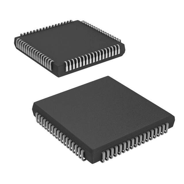
• Available In
- 68 Pin PGA (Commercial, Industrial, and Military)
- 68 Pin PLCC (Commercial and Industrial)
The Intersil 80C286 is a static CMOS version of the NMOS
80286 microprocessor. The 80C286 is an advanced, highperformance microprocessor with specially optimized capabilities for multiple user and multi-tasking systems. The
80C286 has built-in memory protection that supports operating system and task isolation as well as program and data
privacy within tasks. A 25MHz 80C286 provides up to nineteen times the throughput of a standard 5MHz 8086. The
80C286 includes memory management capabilities that map
230 (one gigabyte) of virtual address space per task into 224
bytes (16 megabytes) of physical memory.
The 80C286 is upwardly compatible with 80C86 and 80C88
software (the 80C286 instruction set is a superset of the
80C86/80C88 instruction set). Using the 80C286 real
address mode, the 80C286 is object code compatible with
existing 80C86 and 80C88 software. In protected virtual
address mode, the 80C286 is source code compatible with
80C86 and 80C88 software but may require upgrading to
use virtual address as supported by the 80C286’s integrated
memory management and protection mechanism. Both
modes operate at full 80C286 performance and execute a
superset of the 80C86 and 80C88 instructions.
The 80C286 provides special operations to support the efficient implementation and execution of operating systems.
For example, one instruction can end execution of one task,
save its state, switch to a new task, load its state, and start
execution of the new task. The 80C286 also supports virtual
memory systems by providing a segment-not-present exception and restartable instructions.
Ordering Information
PACKAGE
PGA
PLCC
TEMP. RANGE
10MHz
0oC to +70oC
-
12.5MHz
CG80C286-12
16MHz
CG80C286-16
-40oC to +85oC
IG80C286-10
IG80C286-12
-
-55oC to +125oC
59629067801MXC
59629067802MXC
-
0oC to +70oC
-40oC to +85oC
FN2947 Rev.3.00
January 28, 2008
IS80C286-10
20MHz
CG80C286-20
25MHz
PKG. NO.
-
G68.B
-
-
G68.B
-
-
G68.B
CS80C286-12
CS80C286-16
CS80C286-20
IS80C286-12
IS80C286-16
IS80C286-20
CS80C286-25
-
N68.95
N68.95
Page 1 of 65
�80C286
Pinouts
D12
D13
D14
D4
D5
D6
D7
ERROR
43
45
47
49
51
38
40
42
44
46
48
50
53
52
ERROR
NC
A2
A1
32
33
55
54
NC
BUSY
VCC
CLK
30
31
57
56
INTR
NC
A3
RESET
28
29
59
58
NMI
NC
A5
A4
26
27
61
60
PEREQ
VSS
A7
A6
24
25
63
62
READY
VCC
A9
A8
22
23
65
64
HLDA
HOLD
A11
A10
20
21
67
66
M/IO
COD/INTA
A13
A12
18
19
16
14
12
10
8
6
4
2
68
NC
LOCK
17
15
13
11
9
7
5
3
1
A12
A15
A17
A19
A21
A22
PEACK
S1
NC
A16
A18
A20
VSS
A23
S0
D15
D11
D3
41
36
PIN 1 INDICATOR
BHE
NC
D10
D2
39
34
D9
D1
37
D0
D8
D0
35
A0
A14
VSS
68 LEAD PGA
Component Pad View - As viewed from underside of the component when mounted on the board.
D14
D13
D12
D11
D10
D9
D8
VSS
D7
D6
D5
D4
D3
D2
D1
D0
51
49
47
45
43
41
39
37
35
50
48
46
44
42
40
38
36
34
D0
A0
33
32
A1
A2
VCC
ERROR
52
53
BUSY
NC
54
55
NC
INTR
56
57
31
30
CLK
NC
NMI
58
59
29
28
RESET
A3
VSS
PEREQ
60
61
27
26
A4
A5
VCC
READY
62
63
25
24
A6
A7
14
16
19
18
A12
A13
1
3
5
7
9
11
13
15
17
A12
12
A14
10
A15
8
A16
6
A17
4
A18
2
A19
68
A20
NC
A21
LOCK
VSS
A11
A22
A9
A10
A23
A8
20
PEACK
22
21
S0
23
67
S1
65
66
NC
64
M/IO
NC
HLDA
BHE
HOLD
COD/INTA
PIN 1 INDICATOR
FN2947 Rev.3.00
January 28, 2008
D15
NC
ERROR
68 LEAD PGA
P.C. Board View - As viewed from the component side of the P.C. board.
Page 2 of 65
�80C286
Pinouts
(Continued)
LOCK
M/IO
COD/INTA
HLDA
HOLD
READY
VCC
PEREQ
VSS
NMI
NC
INTR
NC
NC
BUSY
ERROR
NC
68 LEAD PLCC
P.C. Board View - As viewed from the component side of the P.C. board.
PIN 1 INDICATOR
MOLD MARK DOES NOT
INDICATE PIN 1
68 67 66 65 64 63 62 61 60 59 58 57 56 55 54 53 52
BHE
NC
NC
S1
S0
PEACK
A23
A22
VSS
A21
A20
A19
A18
A17
A16
A15
A14
1
2
3
4
5
6
7
8
9
10
11
12
13
14
15
16
17
51
50
49
48
47
46
45
44
43
42
41
40
39
38
37
36
35
D15
D7
D14
D6
D13
D5
D12
D4
D11
D3
D10
D2
D9
D1
D8
D0
VSS
A13
A12
A11
A10
A9
A8
A7
A6
A5
A4
A3
RESET
VCC
CLK
A2
A1
A0
18 19 20 21 22 23 24 25 26 27 28 29 30 31 32 33 34
Functional Diagram
ADDRESS UNIT (AU)
ADDRESS
LATCHES AND DRIVERS
SEGMENT
BASES
OFFSET
ADDER
SEGMENT
LIMIT
SEGMENT
CHECKER
SIZES
PHYSICAL
ADDRESS
ADDER
PREFETCHER
BUS CONTROL
DATA TRANSCEIVERS
6-BYTE
PREFETCH
QUEUE
ALU
REGISTERS CONTROL
PROCESSOR
EXTENSION
INTERFACE
A23 - A0,
BHE, M/IO
PEACK
PEREQ
READY,
HOLD,
S1, S0,
COD/INTA,
LOCK, HLDA
D15 - D0
BUS UNIT (BU)
RESET
3 DECODED
INSTRUCTION
INSTRUCTION
DECODER
QUEUE
INSTRUCTION
UNIT (IU)
CLK
VSS
VCC
EXECUTION UNIT (EU)
NMI
BUSY
INTR ERROR
FN2947 Rev.3.00
January 28, 2008
Page 3 of 65
�80C286
Pin Descriptions
The following pin function descriptions are for the 80C286 microprocessor.
SYMBOL
PIN
NUMBER
TYPE
DESCRIPTION
CLK
31
I
SYSTEM CLOCK: provides the fundamental timing for the 80C286 system. It is divided by two inside
the 80C286 to generate the processor clock. The internal divide-by-two circuitry can be synchronized to an external clock generator by a LOW to HIGH transition on the RESET input.
D15 - D0
36 - 51
I/O
DATA BUS: inputs data during memory, I/O, and interrupt acknowledge read cycles; outputs data
during memory and I/O write cycles. The data bus is active HIGH and is held at high impedance to
the last valid logic level during bus hold acknowledge.
A23 - A0
7-8
10 - 28
32 - 43
O
ADDRESS BUS: outputs physical memory and I/O port addresses. A23 - A16 are LOW during I/O
transfers. A0 is LOW when data is to be transferred on pins D7 - D0 (see table below). The address
bus is active High and floats to three-state off during bus hold acknowledge.
BHE
1
O
BUS HIGH ENABLE: indicates transfer of data on the upper byte of the data bus, D15 - D8. Eight-bit
oriented devices assigned to the upper byte of the data bus would normally use BHE to condition chip
select functions. BHE is active LOW and floats to three-state OFF during bus hold acknowledge.
BHE AND A0 ENCODINGS
S1, S0
4, 5
O
BHE VALUE
A0 VALUE
0
0
Word transfer
0
1
Byte transfer on upper half of data bus (D15 - D8)
1
0
Byte transfer on lower half of data bus (D7 - D0)
1
1
Reserved
FUNCTION
BUS CYCLE STATUS: indicates initiation of a bus cycle and along with M/IO and COD/lNTA, defines the type of bus cycle. The bus is in a TS state whenever one or both are LOW. S1 and S0 are
active LOW and are held at a high impedance logic one during bus hold acknowledge.
80C286 BUS CYCLE STATUS DEFINITION
FN2947 Rev.3.00
January 28, 2008
COD/INTA
M/IO
S1
S0
0(LOW)
0
0
0
Interrupt acknowledge
0
0
0
1
Reserved
0
0
1
0
Reserved
0
0
1
1
None; not a status cycle
0
1
0
0
If A1 = 1 then halt; else shutdown
0
1
0
1
Memory data read
0
1
1
0
Memory data write
0
1
1
1
None; not a status cycle
1(HIGH)
0
0
0
Reserved
1
0
0
1
I/O read
1
0
1
0
I/O write
1
0
1
1
None; not a status cycle
1
1
0
0
Reserved
1
1
0
1
Memory instruction read
1
1
1
0
Reserved
1
1
1
1
None; not a status cycle
BUS CYCLE INITIATED
Page 4 of 65
�80C286
Pin Descriptions
The following pin function descriptions are for the 80C286 microprocessor. (Continued)
SYMBOL
PIN
NUMBER
TYPE
DESCRIPTION
M/IO
67
O
MEMORY I/O SELECT: distinguishes memory access from I/O access. If HIGH during TS, a memory cycle or a halt/shutdown cycle is in progress. If LOW, an I/O cycle or an interrupt acknowledge
cycle is in progress. M/IO is held at high impedance to the last valid logic state during bus hold acknowledge.
COD/lNTA
66
O
CODE/INTERRUPT ACKNOWLEDGE: distinguishes instruction fetch cycles from memory data
read cycles. Also distinguishes interrupt acknowledge cycles from I/O cycles. COD/lNTA is held at
high impedance to the last valid logic state during bus hold acknowledge. Its timing is the same as
M/IO.
LOCK
68
O
BUS LOCK: indicates that other system bus masters are not to gain control of the system bus for
the current and following bus cycles. The LOCK signal may be activated explicitly by the “LOCK”
instruction prefix or automatically by 80C286 hardware during memory XCHG instructions, interrupt
acknowledge, or descriptor table access. LOCK is active LOW and is held at a high impedance logic
one during bus hold acknowledge.
READY
63
l
BUS READY: terminates a bus cycle. Bus cycles are extended without limit until terminated by
READY LOW. READY is an active LOW synchronous input requiring setup and hold times relative
to the system clock be met for correct operation. READY is ignored during bus hold acknowledge.
(See Note 1)
HOLD
HLDA
64
65
I
O
BUS HOLD REQUEST AND HOLD ACKNOWLEDGE: control ownership of the 80C286 local bus.
The HOLD input allows another local bus master to request control of the local bus. When control is
granted, the 80C286 will float its bus drivers and then activate HLDA, thus entering the bus hold acknowledge condition. The local bus will remain granted to the requesting master until HOLD becomes inactive which results in the 80C286 deactivating HLDA and regaining control of the local
bus. This terminates the bus hold acknowledge condition. HOLD may be asynchronous to the system clock. These signals are active HIGH. Note that HLDA never floats.
INTR
57
I
INTERRUPT REQUEST: requires the 80C286 to suspend its current program execution and service
a pending external request. Interrupt requests are masked whenever the interrupt enable bit in the
flag word is cleared. When the 80C286 responds to an interrupt request, it performs two interrupt
acknowledge bus cycles to read an 8-bit interrupt vector that identifies the source of the interrupt.
To ensure program interruption, INTR must remain active until an interrupt acknowledge bus cycle
is initiated. INTR is sampled at the beginning of each processor cycle and must be active HIGH at
least two processor cycles before the current instruction ends in order to interrupt before the next
instruction. INTR is level sensitive, active HIGH, and may be asynchronous to the system clock.
NMI
59
l
NON-MASKABLE INTERRUPT REQUEST: interrupts the 80C286 with an internally supplied vector
value of two. No interrupt acknowledge cycles are performed. The interrupt enable bit in the 80C286
flag word does not affect this input. The NMI input is active HIGH, may be asynchronous to the system clock, and is edge triggered after internal synchronization. For proper recognition, the input must
have been previously LOW for at least four system clock cycles and remain HIGH for at least four
system clock cycles.
PEREQ
PEACK
61
6
l
O
PROCESSOR EXTENSION OPERAND REQUEST AND ACKNOWLEDGE: extend the memory
management and protection capabilities of the 80C286 to processor extensions. The PEREQ input
requests the 80C286 to perform a data operand transfer for a processor extension. The PEACK output signals the processor extension when the requested operand is being transferred. PEREQ is active HIGH. PEACK is active LOW and is held at a high impedance logic one during bus hold
acknowledge. PEREQ may be asynchronous to the system clock.
BUSY
ERROR
54
53
l
I
PROCESSOR EXTENSION BUSY AND ERROR: indicates the operating condition of a processor
extension to the 80C286. An active BUSY input stops 80C286 program execution on WAIT and
some ESC instructions until BUSY becomes inactive (HIGH). The 80C286 may be interrupted while
waiting for BUSY to become inactive. An active ERROR input causes the 80C286 to perform a processor extension interrupt when executing WAIT or some ESC instructions. These inputs are active
LOW and may be asynchronous to the system clock.
FN2947 Rev.3.00
January 28, 2008
Page 5 of 65
�80C286
Pin Descriptions
The following pin function descriptions are for the 80C286 microprocessor. (Continued)
SYMBOL
PIN
NUMBER
TYPE
DESCRIPTION
RESET
29
l
SYSTEM RESET: clears the internal logic of the 80C286 and is active HIGH. The 80C286 may be
reinitialize at any time with a LOW to HIGH transition on RESET which remains active for more than
16 system clock cycles. During RESET active, the output pins of the 80C286 enter the state shown
below.
80C286 PIN STATE DURING RESET
PIN VALUE
PIN NAMES
1 (HIGH)
S0, S1, PEACK, A23 - A0, BHE, LOCK
0 (LOW)
M/IO, COD/lNTA, HLDA (Note 2)
HIGH IMPEDANCE
D15 - D0
Operation of the 80C286 begins after a HlGH to LOW transition on RESET. The HIGH to LOW
transition of RESET must be synchronous to the system clock. Approximately 50 system clock
cycles are required by the 80C286 for internal initializations before the first bus cycle to fetch code
from the power-on execution address is performed. A LOW to HIGH transition of RESET
synchronous to the system clock will end a processor cycle at the second HIGH to LOW transition
of the system clock. The LOW to HIGH transition of RESET may be asynchronous to the system
clock; however, in this case it cannot be predetermined which phase of the processor clock will occur
during the next system clock period. Synchronous LOW to HIGH transitions of RESET are required
only for systems where the processor clock must be phase synchronous to another clock.
VSS
9, 35, 60
l
SYSTEM GROUND: are the ground pins (all must be connected to system ground).
VCC
30, 62
l
SYSTEM POWER: +5V power supply pins. A 0.1F capacitor between pins 60 and 62 is recommended.
NOTES:
1. READY is an open-collector signal and should be pulled inactive with an appropriate resistor (620 at 10MHz and 12.5MHz, 470 at
16MHz, 390 at 20MHz, 270 at 25MHz).
2. HLDA is only Low if HOLD is inactive (Low).
3. All unused inputs should be pulled to their inactive state with pull up/down resistors.
Functional Description
Introduction
The Intersil 80C286 microprocessor is a static CMOS version
of the NMOS 80286 microprocessor. The 80C286 is an
advanced, high-performance microprocessor with specially
optimized capabilities for multiple user and multi-tasking systems. Depending on the application, the 80C286's performance is up to nineteen times faster than the standard 5MHz
8086's, while providing complete upward software compatibility
with Intersil 80C86 and 80C88 CPU family.
The 80C286 operates in two modes: 80C286 real address
mode and protected virtual address mode. Both modes execute a superset of the 80C86 and 80C88 instruction set.
In 80C286 real address mode programs use real addresses with
up to one megabyte of address space. Programs use virtual
addresses in protected virtual address mode, also called protected mode. In protected mode, the 80C286 CPU automatically
maps 1 gigabyte of virtual addresses per task into a 16 megabyte
real address space. This mode also provides memory protection
to isolate the operating system and ensure privacy of each tasks'
programs and data. Both modes provide the same base instruction set, registers and addressing modes.
FN2947 Rev.3.00
January 28, 2008
The Functional Description describes the following: Static operation, the base 80C286 architecture common to both modes,
80C286 real address mode, and finally, protected mode.
Static Operation
The 80C286 is comprised of completely static circuitry. Internal registers, counters, and latches are static and require no
refresh as with dynamic circuit design. This eliminates the
minimum operating frequency restriction typically placed on
microprocessors. The CMOS 80C286 can operate from DC to
the specified upper frequency limit. The clock to the processor may be stopped at any point (either phase one or phase
two of the processor clock cycle) and held there indefinitely.
There is, however, a significant decrease in power requirement if the clock is stopped in phase two of the processor
clock cycle. Details on the clock relationships will be discussed in the Bus Operation section. The ability to stop the
clock to the processor is especially useful for system debug
or power critical applications.
Page 6 of 65
�80C286
The 80C286 can be single-stepped using only the CPU clock.
This state can be maintained as long as necessary. Single step
clock information allows simple interface circuitry to provide
critical information for system debug.
Static design also allows very low frequency operation (down
to DC). In a power critical situation, this can provide low power
operation since 80C286 power dissipation is directly related to
operating frequency. As the system frequency is reduced, so is
the operating power until, ultimately, with the clock stopped in
phase two of the processor clock cycle, the 80C286 power
requirement is the standby current (5mA maximum).
16-BIT
REGISTER
NAME
7
BYTE
ADDRESSABLE
(8-BIT
REGISTER
NAMES
SHOWN)
SPECIAL
REGISTER
FUNCTIONS
07
AX
AH
AL
DX
DH
DL
CX
CH
CL
BX
BH
BL
The 80C86, 80C88, and 80C286 CPU family all contain the
same basic set of registers, instructions, and addressing
modes. The 80C286 processor is upwardly compatible with the
80C86 and 80C88 CPU's.
DI
INDEX REGISTERS
STACK POINTER
SP
15
Register Set
SEGMENT REGISTERS: Four 16-bit special purpose registers
select, at any given time, the segments of memory that are
immediately addressable for code, stack and data. (For usage,
refer to Memory Organization.)
BASE AND INDEX REGISTERS: Four of the general purpose
registers may also be used to determine offset addresses of
operands in memory. These registers may contain base
addresses or indexes to particular locations within a segment.
The addressing mode determines the specific registers used
for operand address calculations.
STATUS AND CONTROL REGISTERS: Three 16-bit special
purpose registers record or control certain aspects of the
80C286 processor state. These include the Flags register and
Machine Status Word register shown in Figure 2, and the
Instruction Pointer, which contains the offset address of the
next sequential instruction to be executed.
FN2947 Rev.3.00
January 28, 2008
LOOP/SHIFT/REPEAT
COUNT
BASE REGISTERS
SI
GENERAL REGISTERS: Eight 16-bit general purpose registers used to contain arithmetic and logical operands. Four of
these (AX, BX, CX and DX) can be used either in their entirety
as 16-bit words or split into pairs of separate 8-bit registers.
MULTIPLY/DIVIDE
I/O INSTRUCTIONS
BP
80C286 Base Architecture
The 80C286 base architecture has fifteen registers as shown
in Figure 1. These registers are grouped into the following four
categories.
0
GENERAL
REGISTERS
15
0
0
CS
CODE SEGMENT
SELECTOR
DS
DATA SEGMENT
SELECTOR
SS
STACK SEGMENT
SELECTOR
ES
EXTRA SEGMENT
SELECTOR
SEGMENT
REGISTERS
15
0
F
IP
MSW
FLAGS
INSTRUCTION
POINTER
MACHINE
STATUS WORD
STATUS AND CONTROL
REGISTERS
FIGURE 1. REGISTER SET
Flags Word Description
The Flags word (Flags) records specific characteristics of the
result of logical and arithmetic instructions (bits 0, 2, 4, 6, 7 and
11) and controls the operation of the 80C286 within a given
operating mode (bits 8 and 9). Flags is a 16-bit register. The
function of the flag bits is given in Table 1.
Page 7 of 65
�80C286
STATUS FLAGS:
CARRY
PARITY
AUXILIARY CARRY
ZERO
SIGN
OVERFLOW
15
FLAGS:
14
13
NT
12
IOPL
11
OF
10
9
8
DF
IF
TF
7
SF
6
5
ZF
4
3
AF
2
1
PF
0
CF
CONTROL FLAGS:
TRAP FLAG
INTERRUPT ENABLE
DIRECTION FLAG
SPECIAL FIELDS:
I/O PRIVILEGE LEVEL
NESTED TASK FLAG
15
MSW:
RESERVED
3
2
1
0
TS
EM
MP
PE
TASK SWITCH
PROCESSOR EXTENSION EMULATED
MONITOR PROCESSOR EXTENSION
PROTECTION ENABLE
FIGURE 2. STATUS AND CONTROL REGISTER BIT FUNCTIONS
TABLE 1. FLAGS WORD BIT FUNCTIONS
BIT POSITION
NAME
0
CF
Carry Flag - Set on high-order bit carry or borrow; cleared otherwise.
2
PF
Parity Flag - Set if low-order 8 bits of result contain an even number of 1 bits; cleared otherwise.
4
AF
Set on carry from or borrow to the low order four bits of AL; cleared otherwise.
6
ZF
Zero Flag - Set if result is zero; cleared otherwise.
7
SF
Sign Flag - Set equal to high-order bit of result (0 if positive, 1 if negative).
11
OF
Overflow Flag - Set if result is a too-large positive number or a too-small negative number (excluding
sign-bit) to fit in destination operand; cleared otherwise.
8
TF
Single Step Flag - Once set, a single step interrupt occurs after the next instruction executes. TF is
cleared by the single step interrupt.
9
IF
Interrupt-Enable Flag - When set, maskable interrupts will cause the CPU to transfer control to an interrupt vector specified location.
10
DF
Direction Flag - Causes string instructions to auto decrement the appropriate index registers when set.
Clearing DF causes auto increment.
FN2947 Rev.3.00
January 28, 2008
FUNCTION
Page 8 of 65
�80C286
Instruction Set
TABLE 2B. ARITHMETIC INSTRUCTIONS
The instruction set is divided into seven categories: data transfer, arithmetic, string manipulation, shift/rotate/logical, high
level, processor control and control transfer instructions. These
categories are summarized in Table 2.
An 80C286 instruction can reference zero, one, or two operands; where an operand may reside in a register, in the
instruction itself, or in memory. Zero-operand instructions (e.g.
NOP and HLT) are usually one byte long. One-operand
instructions (e.g. INC and DEC) are usually two bytes long but
some are encoded in only one byte. One-operand instructions
may reference a register or memory location. Two-operand
instructions permit the following six types of instruction operations:
• Register to Register
• Memory to Register
• Immediate to Register
• Memory to Memory
• Register to Memory
• Immediate to Memory
Two-operand instructions (e.g. MOV and ADD) are usually
three to six bytes long. Memory to memory operations are provided by a special class of string instructions requiring one to
three bytes. For detailed instruction formats and encodings
refer to the instruction set summary at the end of this document.
TABLE 2A. DATA TRANSFER INSTRUCTIONS
GENERAL PURPOSE
ADDITION
ADD
Add byte or word
ADC
Add byte or word with carry
INC
Increment byte or word by 1
AAA
ASClI adjust for addition
DAA
Decimal adjust for addition
SUBTRACTION
SUB
Subtract byte or word
SBB
Subtract byte or word with borrow
DEC
Decrement byte or word by 1
NEG
Negate byte or word
CMP
Compare byte or word
AAS
ASClI adjust for subtraction
DAS
Decimal adjust for subtraction
MULTIPLICATION
MUL
Multiply byte or word unsigned
lMUL
Integer multiply byte or word
AAM
ASClI adjust for multiply
DIVISION
MOV
Move byte or word
DlV
Divide byte or word unsigned
PUSH
Push word onto stack
lDlV
Integer divide byte or word
Pop word off stack
AAD
ASClI adjust for division
PUSHA
Push all registers on stack
CBW
Convert byte to word
POPA
Pop all registers from stack
CWD
Convert word to doubleword
XCHG
Exchange byte or word
XLAT
Translate byte
POP
TABLE 2C. STRING INSTRUCTIONS
INPUT/OUTPUT
IN
OUT
Input byte or word
Output byte or word
ADDRESS OBJECT
LEA
Load effective address
LDS
Load pointer using DS
LES
Load pointer using ES
FLAG TRANSFER
LAHF
Load AH register from flags
SAHF
Store AH register in flags
PUSHF
POPF
Push flags onto stack
MOVS
Move byte or word string
INS
Input bytes or word string
OUTS
Output bytes or word string
CMPS
Compare byte or word string
SCAS
Scan byte or word string
LODS
Load byte or word string
STOS
Store byte or word string
REP
REPE/REPZ
REPNE/REPNZ
Repeat
Repeat while equal/zero
Repeat while not equal/not zero
Pop flags off stack
FN2947 Rev.3.00
January 28, 2008
Page 9 of 65
�80C286
TABLE 2D. SHIFT/ROTATE LOGICAL INSTRUCTIONS
TABLE 2F. PROCESSOR CONTROL INSTRUCTIONS
FLAG OPERATIONS
LOGICALS
NOT
“Not” byte or word
STC
Set carry flag
AND
“And” byte or word
CLC
Clear carry flag
OR
“Inclusive or” byte or word
CMC
Complement carry flag
XOR
“Exclusive or” byte or word
STD
Set direction flag
TEST
“Test” byte or word
CLD
Clear direction flag
STl
Set interrupt enable flag
CLl
Clear interrupt enable flag
SHIFTS
SHL/SAL
Shift logical/arithmetic left byte or word
SHR
Shift logical right byte or word
SAR
Shift arithmetic right byte or word
ROTATES
ROL
Rotate left byte or word
ROR
Rotate right byte or word
RCL
Rotate through carry left byte or word
RCR
Rotate through carry right byte or word
EXTERNAL SYNCHRONIZATION
HLT
Halt until interrupt or reset
WAIT
Wait for TEST pin active
ESC
Escape to extension processor
LOCK
Lock bus during next instruction
NO OPERATION
NOP
No operation
EXECUTION ENVIRONMENT CONTROL
TABLE 2E. HIGH LEVEL INSTRUCTIONS
ENTER
Format stack for procedure entry
LEAVE
Restore stack for procedure exit
BOUND
Detects values outside prescribed range
LMSW
Load machine status word
SMSW
Store machine status word
TABLE 2G. PROGRAM TRANSFER INSTRUCTIONS
CONDITIONAL TRANSFERS
UNCONDITIONAL TRANSFERS
JA/JNBE
Jump if above/not below nor equal
CALL
Call procedure
JAE/JNB
Jump if above or equal/not below
RET
Return from procedure
JB/JNAE
Jump if below/not above nor equal
JMP
Jump
JBE/JNA
Jump if below or equal/not above
JC
JE/JZ
Jump if carry
Jump if equal/zero
ITERATION CONTROLS
LOOP
JG/JNLE
Jump if greater/not less nor equal
JGE/JNL
Jump if greater or equal/not less
LOOPE/LOOPZ
JL/JNGE
Jump if less/not greater nor equal
LOOPNE/LOOPNZ
JLE/JNG
Jump if less or equal/not greater
JCXZ
JNC
JNE/JNZ
JNO
JNP/JPO
Loop
Loop if equal/zero
Loop if not equal/not zero
Jump if register CX = 0
Jump if not carry
Jump if not equal/not zero
Jump if not overflow
INTERRUPTS
INT
Interrupt
Jump if not parity/parity odd
JNS
Jump if not sign
INTO
Interrupt if overflow
JO
Jump if overflow
lRET
Interrupt return
JP/JPE
JS
FN2947 Rev.3.00
January 28, 2008
Jump if parity/parity even
Jump if sign
Page 10 of 65
�80C286
Memory Organization
Addressing Modes
Memory is organized as sets of variable-length segments. Each
segment is a linear contiguous sequence of up to 64K (216) 8-bit
bytes. Memory is addressed using a two-component address (a
pointer) that consists of a 16-bit segment selector and a 16-bit offset. The segment selector indicates the desired segment in memory. The offset component indicates the desired byte address
within the segment. (See Figure 3).
The 80C286 provides a total of eight addressing modes for
instructions to specify operands. Two addressing modes are
provided for instructions that operate on register or immediate
operands:
All instructions that address operands in memory must specify
the segment and the offset. For speed and compact instruction
encoding, segment selectors are usually stored in the high
speed segment registers. An instruction need specify only the
desired segment register and offset in order to address a memory operand.
POINTER
SEGMENT
31
OFFSET
16 15
0
OPERAND
SELECTED
SELECTED
SEGMENT
REGISTER OPERAND MODE: The operand is located in one
of the 8 or 16-bit general registers.
IMMEDIATE OPERAND MODE: The operand is included in
the instruction.
Six modes are provided to specify the location of an operand in a
memory segment. A memory operand address consists of two
16-bit components: segment selector and offset. The segment
selector is supplied by a segment register either implicitly chosen
by the addressing mode or explicitly chosen by a segment override prefix. The offset is calculated by summing any combination
of the following three address elements:
the displacement (an 8 or 16-bit immediate value contained in
the instruction)
the base (contents of either the BX or BP base registers)
the index (contents of either the SI or Dl index registers)
MEMORY
FIGURE 3. TWO COMPONENT ADDRESS
Most instructions need not explicitly specify which segment
register is used. The correct segment register is automatically
chosen according to the rules of Table 3. These rules follow
the way programs are written (see Figure 4) as independent
modules that require areas for code and data, a stack, and
access to external data areas.
Special segment override instruction prefixes allow the implicit
segment register selection rules to be overridden for special
cases. The stack, data and extra segments may coincide for
simple programs. To access operands not residing in one of
the four immediately available segments, a full 32-bit pointer or
a new segment selector must be loaded.
MODULE A
CODE
DATA
MODULE B
CODE
CPU
DATA
CODE
DATA
STACK
PROCESS
STACK
EXTRA
SEGMENT
REGISTERS
TABLE 3. SEGMENT REGISTER SELECTION RULES
MEMORY
REFERENCE
NEEDED
SEGMENT
REGISTER
USED
IMPLICIT SEGMENT
SELECTION RULE
Instructions
Code (CS)
Automatic with instruction prefetch
Stack
Stack (SS) All stack pushes and pops. Any
memory reference which uses BP
as a base register.
Local Data
Data (DS)
All data references except when
relative to stack or string destination
External
(Global) Data
Extra (ES)
Alternate data segment and
destination of string operation
FN2947 Rev.3.00
January 28, 2008
PROCESS
DATA
BLOCK 1
PROCESS
DATA
BLOCK 2
MEMORY
FIGURE 4. SEGMENTED MEMORY HELPS STRUCTURE
SOFTWARE
Any carry out from the 16-bit addition is ignored. Eight-bit displacements are sign extended to 16-bit values.
Page 11 of 65
�80C286
Combinations of these three address elements define the six
memory addressing modes, described below.
DIRECT MODE: The operand's offset is contained in the
instruction as an 8 or 16-bit displacement element.
REGISTER INDIRECT MODE: The operand's offset is in one
of the registers SI, Dl, BX or BP.
BASED MODE: The operand's offset is the sum of an 8 or 16bit displacement and the contents of a base register (BX or
BP).
INDEXED MODE: The operand's offset is the sum of an 8 or 16-bit
displacement and the contents of an index register (SI or Dl).
BASED INDEXED MODE: The operand's offset is the sum of
the contents of a base register and an index register.
BASED INDEXED MODE WITH DISPLACEMENT: The operand's offset is the sum of a base register's contents, an index
register's contents, and an 8 or 16-bit displacement.
Data Types
The 80C286 directly supports the following data types:
Integer:
Ordinal:
Pointer:
String:
ASClI:
A signed binary numeric value contained in an 8-bit
byte or a 16-bit word. All operations assume a 2's
complement representation. Signed 32 and 64-bit
integers are supported using the 80287 Numeric
Data Processor.
An unsigned binary numeric value contained in an
8-bit byte or 16-bit word.
A 32-bit quantity, composed of a segment selector
component and an offset component. Each component is a 16-bit word.
A contiguous sequence of bytes or words. A string
may contain from 1 byte to 64K bytes.
7
SIGN BIT
MAGNITUDE
7
A byte (unpacked) representation of the decimal
digits 0-9.
Packed
BCD:
A byte (packed) representation of two decimal
digits 0-9 storing one digit in each nibble of the byte.
Floating
Point:
A signed 32, 64 or 80-bit real number representation. (Floating point operands are supported using
the 80287 Numeric Processor extension).
Figure 5 graphically represents the data types supported by
the 80C286.
0
UNSIGNED
BYTE
MSB
MAGNITUDE
15 14 +1
0
8 7
0
SIGNED
WORD
SIGN BIT
MSB
SIGNED 31
DOUBLE
WORD
(NOTE)
SIGN BIT
+3
MAGNITUDE
+2 16 15 +1
0
0
MSB
MAGNITUDE
SIGNED 63
QUAD
WORD
(NOTE)
SIGN BIT
+7
+6 +5
48 47
+4 +3
32 31
+2 +1
16 15
0
0
MSB
MAGNITUDE
15
+1
0
0
UNSIGNED
WORD
MSB
MAGNITUDE
BINARY 7
CODED
DECIMAL
(BCD)
+N
0
7
+1
07
0
0
BCD
DIGIT N
7
+N
BCD
DIGIT 1
7
0
+1
BCD
DIGIT 0
07
0
0
ASCII
A byte representation of alphanumeric and control
characters using the ASClI standard of character
representation.
BCD:
0
SIGNED
BYTE
ASCII
CHARACTER1
ASCII
CHARACTERN
7
+N
7
0
PACKED
BCD
+1
ASCII
CHARACTER0
07
0
0
MOST
SIGNIFICANT DIGIT
7/15
+N
0
7/15
LEAST
SIGNIFICANT DIGIT
+1
0 7/15 0
0
STRING
BYTE/WORD N BYTE/WORD 1
31
+3
BYTE/WORD 0
+1 16 15 +1
0
0
POINTER
OFFSET
SELECTOR
79 +9
+8
+7
+6
+5
+4
+3
+2
+1
0 0
FLOATING
POINT (NOTE)
SIGN BIT
EXPONENT
MAGNITUDE
FIGURE 5. 80C286 SUPPORTED DATA TYPES
NOTE: Supported by 80C286/80C287 Numeric Data Processor Configuration
FN2947 Rev.3.00
January 28, 2008
Page 12 of 65
�80C286
TABLE 4. INTERRUPT VECTOR ASSIGNMENTS
FUNCTION
INTERRUPT
NUMBER
RELATED
INSTRUCTIONS
DOES RETURN ADDRESS
POINT TO INSTRUCTION
CAUSING EXCEPTION?
Divide Error Exception
0
DlV, lDlV
Single Step Interrupt
1
All
NMI Interrupt
2
INT 2 or NMI Pin
Breakpoint Interrupt
3
INT 3
INTO Detected Overflow Exception
4
INTO
No
BOUND Range Exceeded Exception
s
BOUND
Yes
Invalid Opcode Exception
6
Any Undefined Opcode
Yes
Processor Extension Not Available Exception
7
ESC or WAIT
Yes
Reserved - Do Not Use
Processor Extension Error Interrupt
Yes
8 - 15
16
Reserved
17 - 31
User Defined
32 - 255
ESC or WAIT
I/O Space
Maskable Interrupt (INTR)
The I/O space consists of 64K 8-bit ports, 32K 16-bit ports, or a
combination of the two. I/O instructions address the I/O space
with either an 8-bit port address, specified in the instruction, or a
16-bit port address in the DX register. 8-bit port addresses are
zero extended such that A15-A8 are LOW. I/O port addresses
00F8(H) through 00FF(H) are reserved.
The 80C286 provides a maskable hardware interrupt request
pin, INTR. Software enables this input by setting the interrupt
flag bit (IF) in the flag word. All 224 user-defined interrupt
sources can share this input, yet they can retain separate interrupt handlers. An 8-bit vector read by the CPU during the interrupt acknowledge sequence (discussed in System Interface
section) identifies the source of the interrupt.
Interrupts
An interrupt transfers execution to a new program location.
The old program address (CS:lP) and machine state (Flags)
are saved on the stack to allow resumption of the interrupted
program. Interrupts fall into three classes: hardware initiated,
INT instructions, and instruction exceptions. Hardware initiated
interrupts occur in response to an external input and are classified as non-maskable or maskable. Programs may cause an
interrupt with an INT instruction. Instruction exceptions occur
when an unusual condition which prevents further instruction
processing is detected while attempting to execute an instruction. The return address from an exception will always point to
the instruction causing the exception and include any leading
instruction prefixes.
A table containing up to 256 pointers defines the proper interrupt service routine for each interrupt. Interrupts 0-31, some of
which are used for instruction exceptions, are reserved. For
each interrupt, an 8-bit vector must be supplied to the 80C286
which identifies the appropriate table entry. Exceptions supply
the interrupt vector internally. INT instructions contain or imply
the vector and allow access to all 256 interrupts. Maskable
hardware initiated interrupts supply the 8-bit vector to the CPU
during an interrupt acknowledge bus sequence. Nonmaskable
hardware interrupts use a predefined internally supplied vector.
FN2947 Rev.3.00
January 28, 2008
The processor automatically disables further maskable interrupts internally by resetting the IF as part of the response to an
interrupt or exception. The saved flag word will reflect the
enable status of the processor prior to the interrupt. Until the
flag word is restored to the flag register, the interrupt flag will
be zero unless specifically set. The interrupt return instruction
includes restoring the flag word, thereby restoring the original
status of IF.
Non-Maskable Interrupt Request (NMI)
A non-maskable interrupt input (NMI) is also provided. NMI has
higher priority than INTR. A typical use of NMI would be to activate a power failure routine. The activation of this input causes
an interrupt with an internally supplied vector value of 2. No
external interrupt acknowledge sequence is performed.
While executing the NMI servicing procedure, the 80C286 will
service neither further NMI requests, INTR requests, nor the
processor extension segment overrun interrupt until an interrupt return (lRET) instruction is executed or the CPU is reset. If
NMI occurs while currently servicing an NMI, its presence will
be saved for servicing after executing the first IRET instruction.
IF is cleared at the beginning of an NMI interrupt to inhibit INTR
interrupts.
Page 13 of 65
�80C286
Single Step Interrupt
The 80C286 has an internal interrupt that allows programs to
execute one instruction at a time. It is called the single step interrupt and is controlled by the single step flag bit (TF) in the flag
word. Once this bit is set, an internal single step interrupt will
occur after the next instruction has been executed. The interrupt
clears the TF bit and uses an internally supplied vector of 1. The
lRET instruction is used to set the TF bit and transfer control to
the next instruction to be single stepped.
takes place and controls the operating mode of the 80C286. It
is a 16-bit register of which the lower four bits are used. One bit
places the CPU into protected mode, while the other three bits,
as shown in Table 7, control the processor extension interface.
After RESET, this register contains FFF0(H) which places the
80C286 in 80C286 real address mode.
TABLE 7. MSW BIT FUNCTIONS
BIT
POSITION
NAME
FUNCTION
0
PE
Protected mode enable places the
80C286 into protected mode and cannot
be cleared except by RESET.
1
MP
Monitor processor extension allows WAIT
instructions to cause a processor extension not present exception (number 7).
2
EM
Emulate processor extension causes a
processor extension not present exception (number 7) on ESC instructions to allow emulating a processor extension.
3
TS
Task switched indicates the next instruction using a processor extension will
cause exception 7, allowing software to
test whether the current processor extension context belongs to the current task.
Interrupt Priorities
When simultaneous interrupt requests occur, they are processed in a fixed order as shown in Table 5. Interrupt processing involves saving the flags, return address, and setting CS:lP
to point at the first instruction of the interrupt handler. If another
enabled interrupt should occur, it is processed before the next
instruction of the current interrupt handler is executed. The last
interrupt processed is therefore the first one serviced.
TABLE 5. INTERRUPT PROCESSING ORDER
ORDER
INTERRUPT
1
Instruction Exception
2
Single Step
3
NMI
4
Processor Extension Segment Overrun
5
INTR
6
INT Instruction
The LMSW and SMSW instructions can load and store the
MSW in real address mode. The recommended use of TS, EM,
and MP is shown in Table 8.
Halt
Initialization and Processor Reset
Processor initialization or start up is accomplished by driving
the RESET input pin HIGH. RESET forces the 80C286 to terminate all execution and local bus activity. No instruction or
bus activity will occur as long as RESET is active. After RESET
becomes inactive, and an internal processing interval elapses,
the 80C286 begins execution in real address mode with the
instruction at physical location FFFFF0(H). RESET also sets
some registers to predefined values as shown in Table 6.
The HLT instruction stops program execution and prevents the
CPU from using the local bus until restarted. Either NMI, INTR
with IF = 1, or RESET will force the 80C286 out of halt. If interrupted, the saved CS:IP will point to the next instruction after
the HLT.
TABLE 6. 80C286 INITIAL REGISTER STATE AFTER RESET
Flag Word
0002(H)
Machine Status Word
FFF0(H)
Instruction Pointer
FFF0(H)
Code Segment
F000(H)
Data Segment
0000(H)
Extra Segment
0000(H)
Stack Segment
0000(H)
HOLD must not be active during the time from the leading
edge of the initial RESET to 34 CLKs after the trailing edge of
the initial RESET of an 80C286 system.
Machine Status Word Description
The machine status word (MSW) records when a task switch
FN2947 Rev.3.00
January 28, 2008
Page 14 of 65
�80C286
TABLE 8. RECOMMENDED MSW ENCODINGS FOR PROCESSOR EXTENSION CONTROL
TS
MP
EM
RECOMMENDED USE
INSTRUCTION
CAUSING
EXCEPTION 7
0
0
0
Initial encoding after RESET. 80C286 operation is identical to 80C86/88.
None
0
0
1
No processor extension is available. Software will emulate its function.
ESC
1
0
1
No processor extension is available. Software will emulate its function. The
current processor extension context may belong to another task.
ESC
0
1
0
A processor extension exists.
None
1
1
0
A processor extension exists. The current processor extension context may
belong to another task. The exception 7 on WAIT allows software to test for
an error pending from a previous processor extension operation.
ESC or WAIT
TABLE 9. REAL ADDRESS MODE ADDRESSING INTERRUPTS
FUNCTION
INTERRUPT
NUMBER
RETURN ADDRESS
BEFORE INSTRUCTION
Interrupt table limit too small exception
8
INT vector is not within table limit
Yes
Processor extension segment overrun
interrupt
9
ESC with memory operand extending beyond offset
FFFF(H)
No
Segment overrun exception
13
Word memory reference with offset = FFFF(H) or an
attempt to execute past the end of a segment
Yes
RELATED INSTRUCTIONS
80C286 Real Address Mode
The 80C286 executes a fully upward-compatible superset of
the 80C86 instruction set in real address mode. In real address
mode the 80C286 is object code compatible with 80C86 and
80C88 software. The real address mode architecture (registers
and addressing modes) is exactly as described in the 80C286
Base Architecture section of this Functional Description.
the segment may be overlaid by another segment to reduce
physical memory requirements.
15
0
0000
OFFSET
ADDRESS
OFFSET
Memory Size
Physical memory is a contiguous array of up to 1,048,576
bytes (one megabyte) addressed by pins A0 through A19 and
BHE. A20 through A23 should be ignored.
15
0
SEGMENT
SELECTOR
SEGMENT
ADDRESS
0000
Memory Addressing
In real address mode physical memory is a contiguous array of
up to 1,048,576 bytes (one megabyte) addressed by pin A0
through A19 and BHE. Address bits A20-A23 may not always
be zero in real mode. A20-A23 should not be used by the system while the 80C286 is operating in Real Mode.
The selector portion of a pointer is interpreted as the upper 16bits of a 20-bit segment address. The lower four bits of the 20bit segment address are always zero. Segment addresses,
therefore, begin on multiples of 16 bytes. See Figure 6 for a
graphic representation of address information.
All segments in real address mode are 64K bytes in size and
may be read, written, or executed. An exception or interrupt
can occur if data operands or instructions attempt to wrap
around the end of a segment (e.g. a word with its low order
byte at offset FFFF(H) and its high order byte at offset
0000(H)). If, in real address mode, the information contained in
a segment does not use the full 64K bytes, the unused end of
FN2947 Rev.3.00
January 28, 2008
ADDER
19
0
20-BIT PHYSICAL
MEMORY ADDRESS
FIGURE 6. 80C286 REAL ADDRESS MODE ADDRESS
CALCULATION
Page 15 of 65
�80C286
Reserved Memory Locations
Protected Virtual Address Mode
The 80C286 reserves two fixed areas of memory in real address
mode (see Figure 7); system initialization area and interrupt
table area. Locations from addresses FFFF0(H) through
FFFFF(H) are reserved for system initialization. Initial execution
begins at location FFFF0(H). Locations 00000(H) through
003FF(H) are reserved for interrupt vectors.
The 80C286 executes a fully upward-compatible superset of
the 80C86 instruction set in protected virtual address mode
(protected mode). Protected mode also provides memory management and protection mechanisms and associated instructions.
RESET BOOTSTRAP
PROGRAM JUMP
INTERRUPT POINTER
FOR VECTOR 255
INTERRUPT POINTER
FOR VECTOR 1
INTERRUPT POINTER
FOR VECTOR 0
FFFFFH
FFFF0H
3FFH
3FCH
7H
4H
3H
0H
The 80C286 enters protected virtual address mode from real
address mode by setting the PE (Protection Enable) bit of the
machine status word with the Load Machine Status Word
(LMSW) instruction. Protected mode offers extended physical
and virtual memory address space, memory protection mechanisms, and new operations to support operating systems and
virtual memory.
All registers, instructions, and addressing modes described in
the 80C286 Base Architecture section of this Functional
Description remain the same. Programs for the 80C86, 80C88,
and real address mode 80C286 can be run in protected mode;
however, embedded constants for segment selectors are different.
Memory Size
FIGURE 7. 80C286 REAL ADDRESS MODE INITIALLY
RESERVED MEMORY LOCATIONS
Interrupts
Table 9 shows the interrupt vectors reserved for exceptions
and interrupts which indicate an addressing error. The exceptions leave the CPU in the state existing before attempting to
execute the failing instruction (except for PUSH, POP, PUSHA,
or POPA). Refer to the next section on protected mode initialization for a discussion on exception 8.
The protected mode 80C286 provides a 1 gigabyte virtual
address space per task mapped into a 16 megabyte physical
address space defined by the address pins A23-A0 and BHE.
The virtual address space may be larger than the physical
address space since any use of an address that does not map
to a physical memory location will cause a restartable exception.
CPU
31
16 15
0
POINTER SELECTOR OFFSET
Protected Mode Initialization
PHYSICAL MEMORY
To prepare the 80C286 for protected mode, the LIDT instruction is used to load the 24-bit interrupt table base and 16-bit
limit for the protected mode interrupt table. This instruction can
also set a base and limit for the interrupt vector table in real
address mode. After reset, the interrupt table base is initialized
to 000000(H) and its size set to 03FF(H). These values are
compatible with 80C86 and 80C88 software. LIDT should only
be executed in preparation for protected mode.
PHYSICAL
ADDRESS
ADDER
MEMORY
OPERAND
Shutdown
Shutdown occurs when a severe error is detected that prevents
further instruction processing by the CPU. Shutdown and halt are
externally signalled via a halt bus operation. They can be distinguished by A1 HIGH for halt and A1 LOW for shutdown. In real
address mode, shutdown can occur under two conditions:
• Exceptions 8 or 13 happen and the IDT limit does not
include the interrupt vector.
• A CALL INT or PUSH instruction attempts to wrap around
the stack segment when SP is not even.
An NMI input can bring the CPU out of shutdown if the IDT limit
is at least 000F(H) and SP is greater than 0005(H), otherwise
shutdown can only be exited via the RESET input.
FN2947 Rev.3.00
January 28, 2008
SEGMENT BASE
ADDRESS
23
SEGMENT
DESCRIPTOR
0
SEGMENT
SEGMENT
DESCRIPTION
TABLE
INITIAL CS:IP VALUE IS F000:FFF0
FIGURE 8. PROTECTED MODE MEMORY ADDRESSING
Memory Addressing
As in real address mode, protected mode uses 32-bit pointers,
consisting of 16-bit selector and offset components. The selector, however, specifies an index into a memory resident table
rather than the upper 16-bits of a real memory address. The
24-bit base address of the desired segment is obtained from
Page 16 of 65
�80C286
the tables in memory. The 16-bit offset is added to the segment base address to form the physical address as shown in
Figure 8. The tables are automatically referenced by the CPU
whenever a segment register is loaded with a selector. All
80C286 instructions which load a segment register will reference the memory based tables without additional software.
The memory based tables contain 8 byte values called
descriptors.
7
0 7
+7
ACCESS
RIGHTS BYTE
+5 P DPL S TYPE A
RESERVED †
+6
BASE 23 - 16
+4
+3
BASE 15 - 0
+1
LIMIT 15 - 0
15
Descriptors
0
8 7
+2
0
0
† MUST BE SET TO 0 FOR COMPATIBILITY WITH FUTURE UPGRADES
Descriptors define the use of memory. Special types of
descriptors also define new functions for transfer of control and
task switching. The 80C286 has segment descriptors for code,
stack and data segments, and system control descriptors for
special system data segments and control transfer operations.
Descriptor accesses are performed as locked bus operations
to assure descriptor integrity in multi-processor systems.
Code and Data Segment Descriptors (S = 1)
Besides segment base addresses, code and data descriptors
contain other segment attributes including segment size (1 to 64K
bytes), access rights (read only, read/write, execute only, and
execute/read), and presence in memory (for virtual memory systems) (See Table 10). Any segment usage violating a segment
attribute indicated by the segment descriptor will prevent the
memory cycle and cause an exception or interrupt.
FIGURE 9. CODE OR DATA SEGMENT DESCRIPTOR
Code and data (including stack data) are stored in two types of
segments: code segments and data segments. Both types are
identified and defined by segment descriptors (S = 1). Code
segments are identified by the executable (E) bit set to 1 in the
descriptor access rights byte. The access rights byte of both
code and data segment descriptor types have three fields in
common: present (P) bit, Descriptor Privilege Level (DPL), and
accessed (A) bit. If P = 0, any attempted use of this segment
will cause a not-present exception. DPL specifies the privilege
level of the segment descriptor. DPL controls when the
descriptor may be used by a task (refer to privilege discussion
below). The A bit shows whether the segment has been previously accessed for usage profiling, a necessity for virtual memory systems. The CPU will always set this bit when accessing
the descriptor.
TABLE 10. CODE AND DATA SEGMENT DESCRIPTOR FORMATS - ACCESS RIGHTS BYTE DEFINITION
BIT
POSITION
7
6-5
4
Present (P)
FUNCTION
P=1
Segment is mapped into physical memory.
P=0
No mapping to physical memory exits, base and limit are not used.
Descriptor Privilege
Level (DPL)
Segment privilege attribute used in privilege tests.
Segment Descriptor (S) S = 1
Code or Data (includes stacks) segment descriptor
S=0
System Segment Descriptor or Gate Descriptor
3
Executable (E)
E=0
Data segment descriptor type is:
2
Expansion Direction
(ED)
ED = 0
Expand up segment, offsets must be limit.
ED = 1
Expand down segment, offsets must be > limit.
Writable (W)
W=0
Data segment may not be written into.
W=1
Data segment may be written into.
1
Type
Field
Definition
NAME
If Data Segment
(S = 1, E = 0)
3
Executable (E)
E=1
Code Segment Descriptor type is:
2
Conforming (C)
C=1
Code segment may only be executed when CPL
DPL and CPL remains unchanged.
1
Readable (R)
R=0
Code segment may not be read.
R=1
Code segment may be read.
A=0
Segment has not been accessed.
A=1
Segment selector has been loaded into segment register or used by selector
test instructions.
0
FN2947 Rev.3.00
January 28, 2008
Accessed (A)
If Code Segment
(S = 1, E = 1)
Page 17 of 65
�80C286
Data segments (S = 1, E = 0) may be either read-only or readwrite as controlled by the W bit of the access rights byte. Readonly (W = 0) data segments may not be written into. Data segments may grow in two directions, as determined by the Expansion Direction (ED) bit: upwards (ED = 0) for data segments, and
downwards (ED = 1) for a segment containing a stack. The limit
field for a data segment descriptor is interpreted differently
depending on the ED bit (see Table 10).
A code segment (S = 1, E = 1) may be execute-only or execute/read as determined by the Readable (R) bit. Code segments may never be written into and execute-only code
segments (R = 0) may not be read. A code segment may also
have an attribute called conforming (C). A conforming code
segment may be shared by programs that execute at different
privilege levels. The DPL of a conforming code segment
defines the range of privilege levels at which the segment may
be executed (refer to privilege discussion below). The limit field
identifies the last byte of a code segment.
TABLE 11. SYSTEM SEGMENT DESCRIPTOR FORMAT FIELDS
NAME
VALUE
TYPE
1
Available Task State Segment (TSS)
2
Local Descriptor Table
3
Busy Task State Segment (TSS)
0
Descriptor contents are not valid
1
Descriptor contents are valid
P
DESCRIPTION
DPL
0-3
Descriptor Privilege Level
BASE
24-Bit
Number
Base Address of special system data
segment in real memory
LIMIT
16-Bit
Number
Offset of last byte in segment
System Segment Descriptors (S = 0, Type = 1-3)
Gate Descriptors (S = 0, Type = 4-7)
In addition to code and data segment descriptors, the protected mode 80C286 defines System Segment Descriptors.
These descriptors define special system data segments which
contain a table of descriptors (Local Descriptor Table Descriptor) or segments which contain the execution state of a task
(Task State Segment Descriptor).
Gates are used to control access to entry points within the target code segment. The gate descriptors are call gates, task
gates, interrupt gates and trap gates. Gates provide a level of
indirection between the source and destination of the control
transfer. This indirection allows the CPU to automatically perform protection checks and control entry point of the destination. Call gates are used to change privilege levels (see
Privilege), task gates are used to perform a task switch, and
interrupt and trap gates are used to specify interrupt service
routines. The interrupt gate disables interrupts (resets IF) while
the trap gate does not.
Table 11 gives the formats for the special system data segment descriptors. The descriptors contain a 24-bit base
address of the segment and a 16-bit limit. The access byte
defines the type of descriptor, its state and privilege level. The
descriptor contents are valid and the segment is in physical
memory if P = 1. If P = 0, the segment is not valid. The DPL
field is only used in Task State Segment descriptors and indicates the privilege level at which the descriptor may be used
(see Privilege). Since the Local Descriptor Table descriptor
may only be used by a special privileged instruction, the DPL
field is not used. Bit 4 of the access byte is 0 to indicate that it
is a system control descriptor. The type field specifies the
descriptor type as indicated in Table 11.
7
+7
0 7
0
+6
RESERVED †
+5 P DPL 0
BASE 23 - 16
TYPE
+3
BASE 15 - 0
+1
LIMIT 15 - 0
15
8 7
+4
+2
0
0
† MUST BE SET TO 0 FOR COMPATIBILITY WITH FUTURE UPGRADES
FIGURE 10. SYSTEM SEGMENT DESCRIPTOR
FN2947 Rev.3.00
January 28, 2008
Table 12 shows the format of the gate descriptors. The descriptor contains a destination pointer that points to the descriptor of
the target segment and the entry point offset. The destination
selector in an interrupt gate, trap gate, and call gate must refer
to a code segment descriptor. These gate descriptors contain
the entry point to prevent a program from constructing and using
an illegal entry point. Task gates may only refer to a task state
segment. Since task gates invoke a task switch, the destination
offset is not used in the task gate.
Exception 13 is generated when the gate is used if a destination
selector does not refer to the correct descriptor type. The word
count field is used in the call gate descriptor to indicate the number of parameters (0-31 words) to be automatically copied from
the caller’s stack to the stack of the called routine when a control
transfer changes privilege levels. The word count field is not
used by any other gate descriptor.
The access byte format is the same for all descriptors. P = 1
indicates that the gate contents are valid. P = 0 indicates the
contents are not valid and causes exception 11 if referenced.
DPL is the descriptor privilege level and specifies when this
descriptor may be used by a task (refer to privilege discussion
below). Bit 4 must equal 0 to indicate a system control descriptor. The type field specifies the descriptor type as indicated in
Table 12.
Page 18 of 65
�80C286
Segment Descriptor Cache Registers
PROGRAM VISIBLE
SEGMENT SELECTORS
A segment descriptor cache register is assigned to each of the
four segment registers (CS, SS, DS, ES). Segment descriptors
are automatically loaded (cached) into a segment descriptor
cache register (Figure 12) whenever the associated segment
register is loaded with a selector.
CS
DS
SS
ES
Only segment descriptors may be loaded into segment
descriptor cache registers. Once loaded, all references to that
segment of memory use the cached descriptor information
instead of reaccessing the descriptor. The descriptor cache
registers are not visible to programs. No instructions exist to
store their contents. They only change when a segment register is loaded.
7
0 7
+3
+1
PROGRAM INVISIBLE
ACCESS
RIGHTS
SEGMENT PHYSICAL
BASE ADDRESS
SEGMENT SIZE
+6
X X X WORD COUNT +4
4-0
X X +2
DESTINATION SELECTOR 15 - 0
+5 P DPL 0
0
0
RESERVED †
+7
15
SEGMENT REGISTERS
(LOADED BY PROGRAM)
TYPE
40 39
16 15
0
SEGMENT DESCRIPTOR CACHE REGISTERS
(AUTOMATICALLY LOADED BY CPU)
0
DESTINATION OFFSET 15 - 0
8 7
47
0
15
† MUST BE SET TO 0 FOR COMPATIBILITY WITH FUTURE UPGRADES
FIGURE 12. DESCRIPTOR CACHE REGISTERS
FIGURE 11. GATE DESCRIPTOR
SELECTOR
INDEX
TABLE 12. GATE DESCRIPTOR FORMAT FIELD
NAME
VALUE
TYPE
4
Call Gate
5
Task Gate
6
Interrupt Gate
7
Trap Gate
0
Descriptor Contents are not valid
1
Descriptor Contents are valid
P
DESCRIPTION
DPL
0-3
Descriptor Privilege Level
WORD
COUNT
0 - 31
Number of words to copy from callers
stack to called procedures stack. Only
used with call gate.
DESTINATION 16-Bit Selector to the target code segment
SELECTOR Selector (call, interrupt or selector Trap Gate).
Selector to the target task state segment (Task Gate).
DESTINATION
OFFSET
16-Bit
Offset
Entry point within the target code segment
Selector Fields
A protected mode selector has three fields: descriptor entry
index, local or global descriptor table indicator (TI), and selector
privilege (RPL) as shown in Figure 13. These fields select one of
two memory based tables of descriptors, select the appropriate
table entry and allow high-speed testing of the selector's privilege attribute (refer to privilege discussion below).
FN2947 Rev.3.00
January 28, 2008
15
BITS
1-0
2
15 - 3
8
NAME
7
TI RPL
2 1
0
FUNCTION
Requested Privilege Level
(RPL)
Indicates Selector Privilege
Level Desired
Table Indicator (TI)
TI = 0 Use Global Descriptor Table (GDT)
TI = 1 Use Local Descriptor
Table (LDT)
Index
Select Descriptor Entry In
Table
FIGURE 13. SELECTOR FIELDS
Local and Global Descriptor Tables
Two tables of descriptors, called descriptor tables, contain all
descriptors accessible by a task at any given time. A descriptor
table is a linear array of up to 8192 descriptors. The upper 13 bits
of the selector value are an index into a descriptor table. Each
table has a 24-bit base register to locate the descriptor table in
physical memory and a 16-bit limit register that confine descriptor
access to the defined limits of the table as shown in Figure 14. A
restartable exception (13) will occur if an attempt is made to reference a descriptor outside the table limits.
One table, called the Global Descriptor table (GDT), contains
descriptors available to all tasks. The other table, called the
Local Descriptor Table (LDT), contains descriptors that can be
private to a task. Each task may have its own private LDT. The
GDT may contain all descriptor types except interrupt and trap
descriptors. The LDT may contain only segment, task gate,
and call gate descriptors. A segment cannot be accessed by a
task if its segment descriptor does not exist in either descriptor
table at the time of access.
Page 19 of 65
�80C286
CPU
MEMORY
MEMORY
GATE FOR
INTERRUPT #n
0
GDT LIMIT
23
GDT
GATE FOR
INTERRUPT #n-1
GDT BASE
24-BIT PHYS AD
15
CPU
0
15
LDT
DESCR
SELECTOR
15
IDT LIMIT
LDT1
CURRENT
LDT
LDT BASE
24-BIT PHYS AD
0
FIGURE 16. INTERRUPT DESCRIPTOR TABLE DEFINITION
LDTn
INCREASING
MEMORY
ADDRESS
PROGRAM INVISIBLE
(AUTOMATICALLY
LOADED
FROM LDT DESCR
WITHIN GDT)
FIGURE 14. LOCAL AND GLOBAL DESCRIPTOR TABLE
DEFINITION
The LGDT and LLDT instructions load the base and limit of the
global and local descriptor tables. LGDT and LLDT are privileged, i.e. they may only be executed by trusted programs
operating at level 0. The LGDT instruction loads a six byte field
containing the 16-bit table limit and 24-bit physical base
address of the Global Descriptor Table as shown in Figure 15.
The LDT instruction loads a selector which refers to a Local
Descriptor Table descriptor containing the base address and
limit for an LDT, as shown in Table 11.
7
0 7
0
BASE 23 - 16
RESERVED †
+5
23
+4
+3
BASE 15 - 0
+2
+1
LIMIT 15 - 0
0
15
8 7
Privilege
The 80C286 has a four-level hierarchical privilege system
which controls the use of privileged instructions and access to
descriptors (and their associated segments) within a task.
Four-level privilege, as shown in Figure 17, is an extension of
the users/supervisor mode commonly found in minicomputers.
The privilege levels are numbered 0 through 3. Level 0 is the
most privileged level. Privilege levels provide protection within
a task. (Tasks are isolated by providing private LDT’s for each
task.) Operating system routines, interrupt handlers, and other
system software can be included and protected within the virtual address space of each task using the four levels of privilege. Each task in the system has a separate stack for each of
its privilege levels.
Tasks, descriptors, and selectors have a privilege level attribute that determines whether the descriptor may be used.
Task privilege affects the use of instructions and descriptors.
Descriptor and selector privilege only affect access to the
descriptor.
CPU
ENFORCED
SOFTWARE
INTERFACES
APPLICATIONS
0
OS EXTENSIONS
† MUST BE SET TO 0 FOR COMPATIBILITY WITH FUTURE UPGRADES
PL = 3
FIGURE 15. GLOBAL DESCRIPTOR TABLE AND INTERRUPT
DESCRlPTOR TABLE DATA TYPE
SYSTEM
SERVICES
Interrupt Descriptor Table
The protected mode 80C286 has a third descriptor table,
called the Interrupt Descriptor Table (IDT) (see Figure 16),
used to define up to 256 interrupts. It may contain only task
gates, interrupt gates and trap gates. The IDT (Interrupt
Descriptor Table) has a 24-bit physical base and 16-bit limit
register in the CPU. The privileged LlDT instruction loads these
registers with a six byte value of identical form to that of the
LGDT instruction (see Figure 16 and Protected Mode lnitialization).
References to IDT entries are made via INT instructions, external
interrupt vectors, or exceptions. The IDT must be at least 256
bytes in size to allocate space for all reserved interrupts.
FN2947 Rev.3.00
January 28, 2008
GATE FOR
INTERRUPT #1
GATE FOR
INTERRUPT #0
IDT BASE
0
LDT LIMIT
23
0
INTERRUPT
DESCRIPTOR
TABLE
(IDT)
INCREASING
MEMORY
ADDRESS
15
HIGH SPEED
OPERATING
SYSTEM
INTERFACE
PL = 2
PL = 1
KERNAL
PL = 0
MOST
PRIVILEGED
NOTE: PL becomes numerically lower as privilege level increases.
FIGURE 17. HIERARCHICAL PRIVILEGE LEVELS
Page 20 of 65
�80C286
Task Privilege
A task always executes at one of the four privilege levels. The
task privilege level at any specific instant is called the Current
Privilege Level (CPL) and is defined by the lower two bits of the
CS register. CPL cannot change during execution in a single
code segment. A task's CPL may only be changed by control
transfers through gate descriptors to a new code segment
(See Control Transfer). Tasks begin executing at the CPL
value specified by the code segment selector within TSS when
the task is initiated via a task switch operation (See Figure 18).
A task executing at Level 0 can access all data segments
defined in the GDT and the task's LDT and is considered the
most trusted level. A task executing a Level 3 has the most
restricted access to data and is considered the least trusted
level.
Descriptor Privilege
Descriptor privilege is specified by the Descriptor Privilege Level
(DPL) field of the descriptor access byte. DPL specifies the least
trusted task privilege level (CPL) at which a task may access the
descriptor. Descriptors with DPL = 0 are the most protected.
Only tasks executing at privilege level 0 (CPL = 0) may access
them. Descriptors with DPL = 3 are the least protected (i.e. have
the least restricted access) since tasks can access them when
CPL = 0, 1, 2, or 3). This rule applies to all descriptors, except
LDT descriptors.
Selector Privilege
Selector privilege is specified by the Requested Privilege Level
(RPL) field in the least significant two bits of a selector. Selector RPL may establish a less trusted privilege level than the
current privilege level for the use of a selector. This level is
called the task's effective privilege level (EPL). RPL can only
reduce the scope of a task's access to data with this selector. A
task's effective privilege is the numeric maximum of RPL and
CPL. A selector with RPL = 0 imposes no additional restriction
on its use while a selector with RPL = 3 can only refer to segments at privilege Level 3 regardless of the task's CPL. RPL is
generally used to verify that pointer parameters passed to a
more trusted procedure are not allowed to use data at a more
privileged level than the caller (refer to pointer testing instructions).
Descriptor Access and Privilege Validation
Determining the ability of a task to access a segment involves
the type of segment to be accessed, the instruction used, the
type of descriptor used and CPL, RPL, and DPL. The two basic
types of segment accesses are control transfer (selectors
loaded into CS) and data (selectors loaded into DS, ES or SS).
Data Segment Access
Instructions that load selectors into DS and ES must refer to a
data segment descriptor or readable code segment descriptor.
The CPL of the task and the RPL of the selector must be the
same as or more privileged (numerically equal to or lower than)
than the descriptor DPL. In general, a task can only access
data segments at the same or less privileged levels than the
CPL or RPL (whichever is numerically higher) to prevent a program from accessing data it cannot be trusted to use.
An exception to the rule is a readable conforming code segment. This type of code segment can be read from any privilege level.
If the privilege checks fail (e.g. DPL is numerically less than the
maximum of CPL and RPL) or an incorrect type of descriptor is
referenced (e.g. gate descriptor or execute only code segment)
exception 13 occurs. If the segment is not present, exception
11 is generated.
Instructions that load selectors into SS must refer to data segment descriptors for writable data segments. The descriptor
privilege (DPL) and RPL must equal CPL. All other descriptor
types or a privilege level violation will cause exception 13. A
not present fault causes exception 12.
TABLE 13. DESCRlPTOR TYPES USED FOR CONTROL TRANSFER
CONTROL TRANSFER TYPES
OPERATION TYPES
DESCRIPTOR
REFERENCED
DESCRIPTOR
TABLE
Intersegment within the same privilege levels
JMP, CALL, RET, lRET (Note 4)
Code Segment
GDT/LDT
Intersegment to the same or higher privilege level interrupt
within task may change CPL
CALL
Call Gate
GDT/LDT
Interrupt Instruction, Exception
External Interrupt
Trap or Interrupt Gate
lDT
Intersegment to a lower privilege level (changes task CPL)
RET, IRET (Note 4)
Code Segment
GDT/LDT
Task Switch
CALL, JMP
Task State Segment
GDT
CALL, JMP
Task Gate
GDT/LDT
lRET (Note 5)
Interrupt Instruction, Exception
External Interrupt
Task Gate
IDT
NOTES:
4. NT (Nested Task bit of flag word) = 0
5. NT (Nested Task bit of flag word) = 1
FN2947 Rev.3.00
January 28, 2008
Page 21 of 65
�80C286
Control Transfer
Privilege Level Changes
Four types of control transfer can occur when a selector is
loaded into CS by a control transfer operation (see Table 13).
Each transfer type can only occur if the operation which loaded
the selector references the correct descriptor type. Any violation of these descriptor usage rules (e.g. JMP through a call
gate or RET to a Task State Segment) will cause exception 13.
Any control transfer that changes CPL within the task, causes
a change of stacks as part of the operation. Initial values of
SS:SP for privilege levels 0, 1, and 2 are kept in the task state
segment (refer to Task Switch Operation). During a JMP or
CALL control transfer, the new stack pointer is loaded into the
SS and SP registers and the previous stack pointer is pushed
onto the new stack.
The ability to reference a descriptor for control transfer is also
subject to rules of privilege. A CALL or JUMP instruction may
only reference a code segment descriptor with DPL equal to
the task CPL or a conforming segment with DPL of equal or
greater privilege than CPL. The RPL of the selector used to
reference the code descriptor must have as much privilege as
CPL.
RET and IRET instructions may only reference code segment
descriptors with descriptor privilege equal to or less privileged
than the task CPL. The selector loaded into CS is the return
address from the stack. After the return, the selector RPL is the
task's new CPL. If CPL changes, the old stack pointer is
popped after the return address.
When a JMP or CALL references a Task State Segment
descriptor, the descriptor DPL must be the same or less privileged than the task's CPL. Reference to a valid Task State
Segment descriptor causes a task switch (see Task Switch
Operation). Reference to a Task State Segment descriptor at a
more privileged level than the task's CPL generates exception
13.
When an instruction or interrupt references a gate descriptor,
the gate DPL must have the same or less privilege than the
task CPL. If DPL is at a more privileged level than CPL, exception 13 occurs. If the destination selector contained in the gate
references a code segment descriptor, the code segment
descriptor DPL must be the same or more privileged than the
task CPL. If not, Exception 13 is issued. After the control transfer, the code segment descriptors DPL is the task's new CPL. If
the destination selector in the gate references a task state segment, a task switch is automatically performed (see Task
Switch Operation).
The privilege rules on control transfer require:
• JMP or CALL direct to a code segment (code segment
descriptor) can only be a conforming segment with DPL of
equal or greater privilege than CPL or a non-conforming segment at the same privilege level.
• Interrupts within the task, or calls that may change privilege
levels, can only transfer control through a gate at the same or
a less privileged level than CPL to a code segment at the
same or more privileged level than CPL.
• Return instructions that don't switch tasks can only return control to a code segment at the same or less privileged level.
• Task switch can be performed by a call, jump or interrupt
which references either a task gate or task state segment at
the same or less privileged level.
FN2947 Rev.3.00
January 28, 2008
When returning to the original privilege level, its stack is
restored as part of the RET or IRET instruction operation. For
subroutine calls that pass parameters on the stack and cross
privilege levels, a fixed number of words, as specified in the
gate, are copied from the previous stack to the current stack.
The inter-segment RET instruction with a stack adjustment
value will correctly restore the previous stack pointer upon
return.
Protection
The 80C286 includes mechanisms to protect critical instructions that effect the CPU execution state (e.g. HLT) and code
or data segments from improper usage. These protection
mechanisms are grouped into three forms:
• Restricted usage of segments (e.g. no write allowed to readonly data segments). The only segments available for use are
defined by descriptors in the Local Descriptor Table (LDT)
and Global Descriptor Table (GDT).
• Restricted access to segments via the rules of privilege and
descriptor usage.
• Privileged instructions or operations that may only be executed at certain privilege levels as determined by the CPL and
I/O Privilege Level (lOPL). The lOPL is defined by bits 14 and
13 of the flag word.
These checks are performed for all instructions and can be
split into three categories: segment load checks (Table 14),
operand reference checks (Table 15), and privileged instruction checks (Table 16). Any violation of the rules shown will
result in an exception. A not-present exception related to the
stack segment causes exception 12.
TABLE 14. SEGMENT REGISTER LOAD CHECKS
EXCEPTION
NUMBER
ERROR DESCRIPTION
Descriptor table limit exceeded
13
Segment descriptor not-present
11 or 12
Privilege rules violated
13
Invalid descriptor/segment type segment register
load:
- Read only data segment load to SS
- Special control descriptor load to DS, ES, SS
- Execute only Segment load to DS, ES, SS
- Data segment load to CS
- Read/Execute code segment load SS
13
Page 22 of 65
�80C286
TABLE 15. OPERAND REFERENCE CHECKS
EXCEPTION
NUMBER
ERROR DESCRIPTION
Write into code segment
13
Read from execute-only code segment
13
Write to read-only data segment
13
Segment limit exceeded (See Note)
12 or 13
NOTE: Carry out in offset calculations is ignored.
TABLE 16. PRIVILEGED INSTRUCTION CHECKS
EXCEPTION
NUMBER
ERROR DESCRIPTION
CPL 0 when executing the following instructions:
LIDT, LLDT, LGDT, LTR, LMSW, CTS, HLT
13
CPT > IOPL when executing the following
instructions:
INS, IN, OUTS, OUT, STI, CLI, LOCK
13
The lRET and POPF instructions do not perform some of
their defined functions if CPL is not of sufficient privilege
(numerically small enough). Precisely these are:
• The IF bit is not changed if CPL is greater than IOPL.
• The lOPL field of the flag word is not changed if CPL is
greater than 0.
No exceptions or other indication are given when these conditions occur.
Exceptions
The 80C286 detects several types of exceptions and interrupts in protected mode (see Table 17). Most are restartable
after the exceptional condition is removed. Interrupt handlers
for most exceptions can read an error code, pushed on the
stack after the return address, that identifies the selector
involved (0 if none). The return address normally points to
the failing instruction including all leading prefixes. For a processor extension segment overrun exception, the return
address will not point at the ESC instruction that caused the
exception; however, the processor extension registers may
contain the address of the failing instruction.
These exceptions indicate a violation to privilege rules or
usage rules has occurred. Restart is generally not attempted
under those conditions.
All these checks are performed for all instructions and can
be split into three categories: segment load checks (Table
14), operand reference checks (Table 15), and privileged
instruction checks (Table 16). Any violation of the rules
shown will result in an exception. A not-present exception
causes exception 11 or 12 and is restartable.
SPECIAL OPERATIONS
Task Switch Operation
The 80C286 provides a built-in task switch operation which
saves the entire 80C286 execution state (registers, address
space, and a link to the previous task), loads a new execution
state, and commences execution in the new task. Like gates,
the task switch operation is invoked by executing an inter-segment JMP or CALL instruction which refers to a Task State
Segment (TSS) or task gate descriptor in the GDT or LDT. An
INT instruction, exception, or external interrupt may also
invoke the task switch operation by selecting a task gate
descriptor in the associated IDT descriptor entry.
The TSS descriptor points at a segment (see Figure 18) containing the entire 80C286 execution state while a task gate
descriptor contains a TSS selector. The limit field of the
descriptor must be greater than 002B(H).
Each task must have a TSS associated with it. The current
TSS is identified by a special register in the 80C286 called
the Task Register (TR). This register contains a selector
referring to the task state segment descriptor that defines
the current TSS. A hidden base and limit register associated
with TR are loaded whenever TR is loaded with a new selector. The IRET instruction is used to return control to the task
that called the current task or was interrupted. Bit 14 in the
flag register is called the Nested Task (NT) bit. It controls the
TABLE 17. PROTECTED MODE EXCEPTIONS
INTERRUPT
VECTOR
FUNCTION
RETURN ADDRESS
AT FALLING
INSTRUCTION?
ALWAYS
RESTARTABLE?
ERROR CODE
ON STACK?
8
Double exception detected
Yes
No (Note 7)
Yes
9
Processor extension segment overrun
No
No (Note 7)
No
10
Invalid task state segment
Yes
Yes
Yes
11
Segment not present
Yes
Yes
Yes
12
Stack segment overrun or stack segment not present
Yes
Yes (Note 6)
Yes
13
General protection
Yes
No (Note 7)
Yes
NOTES:
6. When a PUSHA or POPA instruction attempts to wrap around the stack segment, the machine state after the exception will not be restartable
because stack segment wrap around is not permitted. This condition is identified by the value of the saved SP being either 0000(H), 0001(H),
FFFE(H), or FFFF(H).
7. These exceptions indicate a violation to privilege rules or usage rules has occurred. Restart is generally not attempted under those conditions.
FN2947 Rev.3.00
January 28, 2008
Page 23 of 65
�80C286
function of the IRET instruction. If NT = 0, the IRET instruction
performs the regular current task by popping values off the
stack; when NT = 1, IRET performs a task switch operation
back to the previous task.
When a CALL, JMP, or INT instruction initiates a task switch,
the old (except for case of JMP) and new TSS will be marked
busy and the back link field of the new TSS set to the old TSS
selector. The NT bit of the new task is set by CALL or INT initiated task switches. An interrupt that does not cause a task
switch will clear NT. NT may also be set or cleared by POPF or
IRET instructions.
The task state segment is marked busy by changing the
descriptor type field from Type 1 to Type 3. Use of a selector
that references a busy task state segment causes Exception
13.
Processor Extension Context Switching
The context of a processor extension is not changed by the task
switch operation. A processor extension context need only be
changed when a different task attempts to use the processor
extension (which still contains the context of a previous task).
The 80C286 detects the first use of a processor extension after
a task switch by causing the processor extension not present
exception (7). The interrupt handler may then decide whether a
context change is necessary.
Whenever the 80C286 switches tasks, it sets the Task
Switched (TS) bit of the MSW. TS indicates that a processor
extension context may belong to a different task than the current one. The processor extension not present exception (7)
will occur when attempting to execute an ESC or WAIT
instruction if TS = 1 and a processor extension is present (MP
= 1 in MSW).
Pointer Testing Instructions
The 80C286 provides several instructions to speed pointer testing and consistency checks for maintaining system integrity (see
Table 18). These instructions use the memory management
hardware to verify that a selector value refers to an appropriate
segment without risking an exception. A condition flag (ZF) indicates whether use of the selector or segment will cause an
exception.
Double Fault and Shutdown
If two separate exceptions are detected during a single instruction execution, the 80C286 performs the double fault exception
(8). If an exception occurs during processing of the double fault
exception, the 80C286 will enter shutdown. During shutdown
no further instructions or exceptions are processed. Either NMI
(CPU remains in protected mode) or RESET (CPU exits protected mode) can force the 80C286 out of shutdown. Shutdown is externally signalled via a HALT bus operation with A1
LOW.
Protected Mode lnitialization
The 80C286 initially executes in real address mode after
RESET. To allow initialization code to be placed at the top of
physical memory. A23-20 will be HIGH when the 80C286 performs memory references relative to the CS register until CS is
changed. A23-20 will be zero for references to the DS, ES, or
SS segments. Changing CS in real address mode will force
A23-20 LOW whenever CS is used again. The initial CS:lP
value of F000:FFF0 provides 64K bytes of code space for initialization code without changing CS.
Protected mode operation requires several registers to be initialized. The GDT and IDT base registers must refer to a valid
GDT and IDT. After executing the LMSW instruction to set PE,
the 80C286 must immediately execute an intrasegment JMP
instruction to clear the instruction queue of instructions
decoded in real address mode.
To force the 80C286 CPU registers to match the initial protected mode state assumed by software, execute a JMP
instruction with a selector referring to the initial TSS used in the
system. This will load the task register, local descriptor table
register, segment registers and initial general register state.
The TR should point at a valid TSS since any task switch operation involves saving the current task state.
TABLE 18. 80C286 POINTER TEST INSTRUCTIONS
INSTRUCTION
OPERANDS
FUNCTION
ARPL
Selector,
Register
Adjust Requested Privilege Level: adjusts the RPL of the selector to the numeric maximum of
current selector RPL value and the RPL value in the register. Set zero flag if selector RPL was
changed by ARPL.
VERR
Selector
VERify for Read: sets the zero flag if the segment referred to by the selector can be read.
VERW
Selector
VERify for Write: sets the zero flag if the segment referred to by the selector can be written.
LSL
Register,
Selector
Load Segment Limit: reads the segment limit into the register if privilege rules and descriptor type
allow. Set zero flag if successful.
LAR
Register,
Selector
Load Access Rights: reads the descriptor access rights byte into the register if privilege rules allow. Set zero flag if successful.
FN2947 Rev.3.00
January 28, 2008
Page 24 of 65
�80C286
CPU
RESERVED
TASK REGISTER
TR
15
0
SYSTEM
SEGMENT
DESCRIPTOR
P D 0 TYPE
P
L
BASE 23 - 16
DESCRIPTION
1
An available task state segment.
May be used as the destination
of a task switch operation.
3
A busy task state segment. Cannot be used as the destination of
a task switch.
DESCRIPTION
BASE 15 - 0
PROGRAM INVISIBLE
15
TYPE
LIMIT 15 - 0
0
LIMIT
BASE
23
0
15
TASK
STATE
SEGMENT
0
BYTE
OFFSET
TASK LDT SELECTOR
42
DS SELECTOR
40
P
SS SELECTOR
38
1
Base and Limit fields are valid.
CS SELECTOR
36
ES SELECTOR
0
34
DI
32
Segment is not present in memory, Base and Limit are not defined.
SI
30
BP
28
SP
26
BX
24
DX
22
CX
20
AX
18
FLAG WORD
16
IP (ENTRY POINT)
14
SS FOR CPL 2
12
SP FOR CPL 2
10
SS FOR CPL 1
8
SP FOR CPL 1
6
SS FOR CPL 0
4
SP FOR CPL 0
2
CURRENT
TASK
STATE
INITIAL
STACKS
FOR CPL 0, 1, 2
BACK LINK SELECTOR TO TSS 0
FIGURE 18. TASK STATE SEGMENT AND TSS REGISTERS
FN2947 Rev.3.00
January 28, 2008
Page 25 of 65
�80C286
System Interface
The 80C286 system interface appears in two forms: a local bus
and a system bus. The local bus consists of address, data, status, and control signals at the pins of the CPU. A system bus is
any buffered version of the local bus. A system bus may also differ from the local bus in terms of coding of status and control
lines and/or timing and loading of signals.
OUTPUT
DRIVER
BOND
PAD
VCC
EXTERNAL
PIN
P
Bus Interface Signals and Timing
The 80C286 microsystems local bus interfaces the 80C286 to
local memory and I/O components. The interface has 24
address lines, 16 data lines, and 8 status and control signals.
The 80C286 CPU, 82C284 clock generator, 82C288 bus controller, 82289 bus arbiter, 82C86H/87H transceivers, and
82C82/83H latches provide a buffered and decoded system
bus interface. The 82C284 generates the system clock and
synchronizes READY and RESET. The 82C288 converts bus
operation status encoded by the 80C286 into command and
bus control signals. The 82289 bus arbiter generates Multibus™ bus arbitration signals. These components can provide
the critical timing required for most system bus interfaces
including the Multibus.
Bus Hold Circuitry
To avoid high current conditions caused by floating inputs to
CMOS devices, and to eliminate the need for pull-up/down
resistors, “bus-hold” circuitry has been used on the 80C286
pins 4-6, 36-51 and 66-68 (See Figure 19A and 19B). The circuit shown in Figure 19A will maintain the last valid logic state
if no driving source is present (i.e. an unconnected pin or a
driving source which goes to a high impedance state). The circuit shown in Figure 19B will maintain a high impedance logic
one state if no driving source is present. To overdrive the “bushold” circuits, an external driver must be capable of sinking or
sourcing approximately 400 microamps at valid input voltage
levels. Since this “bus-hold” circuitry is active and not a “resistive” type element, the associated power supply current is negligible, and power dissipation is significantly reduced when
compared to the use of passive pull-up resistors.
BOND
PAD
EXTERNAL
PIN
OUTPUT
DRIVER
INPUT
DRIVER
INPUT
PROTECTION
CIRCUITRY
FIGURE 19B. BUS HOLD CIRCUITRY, PINS 4-6, 68
Physical Memory and I/O Interface
A maximum of 16 megabytes of physical memory can be
addressed in protected mode. One megabyte can be addressed
in real address mode. Memory is accessible as bytes or words.
Words consist of any two consecutive bytes addressed with the
least significant byte stored in the lowest address. Byte transfers
occur on either half of the 16-bit local data bus. Even bytes are
accessed over D7-0 while odd bytes are transferred over D15-8.
Even addressed words are transferred over D15-0 in one bus
cycle, while odd addressed word require two bus operations.
The first transfers data on D15-8, and the second transfers data
on D7-0. Both byte data transfers occur automatically, transparent to software.
Two bus signals, A0 and BHE, control transfers over the lower
and upper halves of the data bus. Even address byte transfers
are indicated by A0 LOW and BHE HIGH. Odd address byte
transfers are indicated by A0 HlGH and BHE LOW. Both A0
and BHE are LOW for even address word transfers.
The I/O address space contains 64K addresses in both modes.
The I/O space is accessible as either bytes or words, as is memory. Byte wide peripheral devices may be attached to either the
upper or lower byte of the data bus. Byte-wide I/O devices
attached to the upper data byte (D15-8) are accessed with odd
I/O addresses. Devices on the lower data byte are accessed
with even I/O addresses. An interrupt controller such as Intersil's
82C59A must be connected to the lower data byte (D7-0) for
proper return of the interrupt vector.
Bus Operation
INPUT
PROTECTION
CIRCUITRY
FIGURE 19A. BUS HOLD CIRCUITRY, PINS 36-51, 66, 67
FN2947 Rev.3.00
January 28, 2008
INPUT
DRIVER
The 80C286 uses a double frequency system clock (CLK
input) to control bus timing. All signals on the local bus are
measured relative to the system CLK input. The CPU divides
the system clock by 2 to produce the internal processor clock,
which determines bus state. Each processor clock is composed of two system clock cycles named phase 1 and phase 2.
The 82C284 clock generator output (PCLK) identifies the next
phase of the processor clock. (See Figure 20.)
Page 26 of 65
�80C286
During hold (TH), the 80C286 will float all address, data, and
status output drivers enabling another bus master to use the
local bus. The 80C286 HOLD input signal is used to place the
80C286 into the TH state. The 80C286 HLDA output signal
indicates that the CPU has entered TH.
ONE PROCESSOR CLOCK CYCLE
ONE BUS T STATE
PHASE 1
OF PROCESSOR
CLOCK CYCLE
PHASE 2
OF PROCESSOR
CLOCK CYCLE
Pipelined Addressing
CLK
ONE SYSTEM
CLK CYCLE
PCLK
FIGURE 20. SYSTEM AND PROCESSOR CLOCK RELATIONSHIPS
Six types of bus operations are supported; memory read,
memory write, I/O read, I/O write, interrupt acknowledge, and
halt/shutdown. Data can be transferred at a maximum rate of
one word per two processor clock cycles.
The 80C286 bus has three basic states: idle (TI), send status
(TS), and perform command (TC). The 80C286 CPU also has a
fourth local bus state called hold (TH). TH indicates that the
80C286 has surrendered control of the local bus to another
bus master in response to a HOLD request.
Each bus state is one processor clock long. Figure 21 shows
the four 80C286 local bus states and allowed transitions.
RESET
HLDA
NEW CYCLE HLDA
HLDA
HOLD
TH
IDLE
TI
HLDA NEW CYCLE
READY NEW CYCLE
NEW CYCLE
READY
HLDA NEW CYCLE
ALWAYS
STATUS
TS
COMMAND
TC
READY NEW CYCLE
FIGURE 21. 80C286 BUS STATES
Bus States
The idle (TI) state indicates that no data transfers are in progress or requested. The first active state TS is signaled by status line S1 or S0 going LOW and identifying phase 1 of the
processor clock. During TS, the command encoding, the
address, and data (for a write operation) are available on the
80C286 output pins. The 82C288 bus controller decodes the
status signals and generates Multibus compatible read/write
command and local transceiver control signals.
After TS, the perform command (TC) state is entered. Memory
or I/O devices respond to the bus operation during TC , either
transferring read data to the CPU or accepting write data. TC
states may be repeated as often as necessary to ensure sufficient time for the memory or I/O device to respond. The
READY signal determines whether TC is repeated. A repeated
TC state is called a wait state.
FN2947 Rev.3.00
January 28, 2008
The 80C286 uses a local bus interface with pipelined timing to
allow as much time as possible for data access. Pipelined timing allows a new bus operation to be initiated every two processor cycles, while allowing each individual bus operation to
last for three processor cycles.
The timing of the address outputs is pipelined such that the
address of the next bus operation becomes available during the
current bus operation. Or, in other words, the first clock of the
next bus operation is overlapped with the last clock of the current bus operation. Therefore, address decode and routing logic
can operate in advance of the next bus operation.
External address latches may hold the address stable for the
entire bus operation, and provide additional AC and DC buffering.
The 80C286 does not maintain the address of the current bus
operation during all TC states. Instead, the address for the next
bus operation may be emitted during phase 2 of any TC . The
address remains valid during phase 1 of the first TC to guarantee hold time, relative to ALE, for the address latch inputs.
Bus Control Signals
The 82C288 bus controller provides control signals; address
latch enable (ALE), Read/Write commands, data transmit/receive (DT/R), and data enable (DEN) that control the
address latches, data transceivers, write enable, and output
enable for memory and I/O systems.
The Address Latch Enable (ALE) output determines when the
address may be latched. ALE provides at least one system
CLK period of address hold time from the end of the previous
bus operation until the address for the next bus operation
appears at the latch outputs. This address hold time is required
to support Multibus and common memory systems.
The data bus transceivers are controlled by 82C288 outputs
Data Enable (DEN) and Data Transmit/Receive (DT/R). DEN
enables the data transceivers; while DT/R controls transceiver
direction. DEN and DT/R are timed to prevent bus contention
between the bus master, data bus transceivers, and system
data bus transceivers.
Command Timing Controls
Two system timing customization options, command extension
and command delay, are provided on the 80C286 local bus.
Command extension allows additional time for external devices
to respond to a command and is analogous to inserting wait
states on the 80C86. External logic can control the duration of
any bus operation such that the operation is only as long as
necessary. The READY input signal can extend any bus operation for as long as necessary.
Command delay allows an increase of address or write data
Page 27 of 65
�80C286
less. To customize system bus timing, an address decoder can
determine which bus operations require delaying the command. The CMDLY input does not affect the timing of ALE,
DEN or DT/R.
setup time to system bus command active for any bus operation by delaying when the system bus command becomes
active. Command delay is controlled by the 82C288 CMDLY
input. After TS, the bus controller samples CMDLY at each failing edge of CLK. If CMDLY is HIGH, the 82C288 will not activate the command signal. When CMDLY is LOW, the 82C288
will activate the command signal. After the command becomes
active, the CMDLY input is not sampled.
Figure 23 illustrates four uses of CMDLY. Example 1 shows
delaying the read command two system CLKs for cycle N-1
and no delay for cycle N, and example 2 shows delaying the
read command one system CLK for cycle N-1 and one system
CLK delay for cycle N.
When a command is delayed, the available response time from
command active to return read data or accept write data is
READ BUS CYCLE N
TI
TS
1
READ BUS CYCLE N + 1
TC
2
1
TS
2
1
TC
2
1
2
CLK
PROC
CLK
2 PCLK CYCLE TRANSFER
2 PCLK CYCLE TRANSFER
2.5 CLOCK CYCLE ADDRESS TO DATA VALID
A23 - A0
VALID ADDR (N)
VALID ADDR (N + 1)
S0 S1
READY
D15 - D0
VALID READ
DATA (N)
VALID READ
DATA (N + 1)
PIPELINING: VALID ADDRESS (N + 1) AVAILABLE IN LAST PHASE OF BUS CYCLE (N).
FIGURE 22. BASIC BUS CYCLE
FN2947 Rev.3.00
January 28, 2008
Page 28 of 65
�80C286
READ CYCLE N -1
TS
1
READ CYCLE N
TC
2
1
TC
2
1
TS
2
1
TC
2
1
2
CLK
PROC
CLK
A23 - A0
VALID ADDR (N-1)
VALID ADDR N
S1 S0
ALE
READY
RD
EX1
CMDLY
RD
EX2
CMDLY
FIGURE 23. CMDLY CONTROLS THE LEADING EDGE OF COMMAND SIGNAL
Bus Cycle Termination
At maximum transfer rates, the 80C286 bus alternates
between the status and command states. The bus status signals become inactive after TS so that they may correctly signal
the start of the next bus operation after the completion of the
current cycle. No external indication of TC exists on the
80C286 local bus. The bus master and bus controller enter TC
directly after TS and continue executing TC cycles until terminated by the assertion of READY.
READY Operation
The current bus master and 82C288 bus controller terminate
each bus operation simultaneously to achieve maximum bus
operation bandwidth. Both are informed in advance by READY
active (open-collector output from 82C284) which identifies the
last TC cycle of the current bus operation. The bus master and
bus controller must see the same sense of the READY signal,
thereby requiring READY to be synchronous to the system
clock.
Synchronous Ready
The 82C284 clock generator provides READY synchronization
from both synchronous and asynchronous sources (see Figure
24). The synchronous ready input (SRDY) of the clock generator is sampled with the falling edge of CLK at the end of phase
FN2947 Rev.3.00
January 28, 2008
1 of each TC. The state of SRDY is then broadcast to the bus
master and bus controller via the READY output line.
Asynchronous Ready
Many systems have devices or subsystems that are asynchronous to the system clock. As a result, their ready outputs cannot be guaranteed to meet the 82C284 SRDY setup and hold
time requirements. But the 82C284 asynchronous ready input
(ARDY) is designed to accept such signals. The ARDY input is
sampled at the beginning of each TC cycle by 82C284 synchronization logic. This provides one system CLK cycle time to
resolve its value before broadcasting it to the bus master and
bus controller.
ARDY or ARDYEN must be HIGH at the end of TS. ARDY cannot be used to terminate the bus cycle with no wait states.
Each ready input of the 82C284 has an enable pin (SRDYEN
and ARDYEN) to select whether the current bus operation will
be terminated by the synchronous or asynchronous ready.
Either of the ready inputs may terminate a bus operation.
These enable inputs are active low and have the same timing
as their respective ready inputs. Address decode logic usually
selects whether the current bus operation should be terminated by ARDY or SRDY.
Data Bus Control
Page 29 of 65
�80C286
Figures 25, 26, and 27 show how the DT/R, DEN, data bus,
and address signals operate for different combinations of read,
write, and idle bus operations. DT/R goes active (LOW) for a
read operation. DT/R remains HIGH before, during, and
between write operations.
The data bus is driven with write data during the second phase
of TS . The delay in write data timing allows the read data drivers, from a previous read cycle, sufficient time to enter threestate OFF before the 80C286 CPU begins driving the local
data bus for write operations. Write data will always remain
valid for one system clock past the last TC to provide sufficient
hold time for Multibus or other similar memory or I/O systems.
During write-read or write-idle sequences the data bus enters a
high impedance state during the second phase of the processor cycle after the last TC . In a write-write sequence the data
bus does not enter a high impedance state between TC and
TS.
Bus Usage
The 80C286 local bus may be used for several functions:
instruction data transfers, data transfers by other bus masters, instruction fetching, processor extension data transfers,
interrupt acknowledge, and halt/shutdown. This section
describes local bus activities which have special signals or
requirements. Note that I/O transfers take place in exactly the
same manner as memory transfers (i.e. to the 80C286 the
timing, etc. of an I/O transfer is identical to a memory transfer).
HOLD and HLDA
HOLD and HLDA allow another bus master to gain control of the
local bus by placing the 80C286 bus into the TH state. The
sequence of events required to pass control between the
80C286 and another local bus master are shown in Figure 28.
In this example, the 80C286 is initially in the TH state as signaled by HLDA being active. Upon leaving TH, as signaled by
HLDA going inactive, a write operation is started. During the
write operation another local bus master requests the local
bus from the 80C286 as shown by the HOLD signal. After
completing the write operation, the 80C286 performs one TI
bus cycle, to guarantee write data hold time, then enters TH
as signaled by HLDA going active.
prefix is used. The LOCK prefix may be used with the following ASM-286 assembly instructions; MOVS, INS and OUTS.
For bus cycles other than Interrupt-Acknowledge cycles, Lock
will be active for the first and subsequent cycles of a series of
cycles to be locked. Lock will not be shown active during the
last cycle to be locked. For the next-to-last cycle, Lock will
become inactive at the end of the first TC regardless of the
number of wait states inserted. For Interrupt-Acknowledge
cycles, Lock will be active for each cycle, and will become
inactive at the end of the first TC for each cycle regardless of
the number of wait-states inserted.
Instruction Fetching
The 80C286 Bus Unit (BU) will fetch instructions ahead of the
current instruction being executed. This activity is called
prefetching. It occurs when the local bus would otherwise be
idle and obeys the following rules:
A prefetch bus operation starts when at least two bytes of the
6-byte prefetch queue are empty.
The prefetcher normally performs word prefetches independent of the byte alignment of the code segment base in physical memory.
The prefetcher will perform only a byte code fetch operation for
control transfers to an instruction beginning on a numerically
odd physical address.
Prefetching stops whenever a control transfer or HLT instruction is decoded by the lU and placed into the instruction queue.
In real address mode, the prefetcher may fetch up to 6 bytes
beyond the last control transfer or HLT instruction in a code
segment.
In protected mode, the prefetcher will never cause a segment
overrun exception. The prefetcher stops at the last physical
memory word of the code segment. Exception 13 will occur if
the program attempts to execute beyond the last full instruction
in the code segment.
If the last byte of a code segment appears on an even physical
memory address, the prefetcher will read the next physical
byte of memory (perform a word code fetch). The value of this
byte is ignored and any attempt to execute it causes exception
13.
The CMDLY signal and ARDY ready are used to start and stop
the write bus command, respectively. Note that SRDY must be
inactive or disabled by SRDYEN to guarantee ARDY will terminate the cycle.
HOLD must not be active during the time from the leading
edge of RESET until 34 CLKs following the trailing edge of
RESET unless the 80C286 is in the Halt condition. To ensure
that the 80C286 remains in the Halt condition until the processor Reset operation is complete, no interrupts should occur
after the execution of HLT until 34 CLKs after the trailing edge
of the RESET pulse.
LOCK
The CPU asserts an active lock signal during InterruptAcknowledge cycles, the XCHG instruction, and during some
descriptor accesses. Lock is also asserted when the LOCK
FN2947 Rev.3.00
January 28, 2008
Page 30 of 65
�80C286
MEMORY CYCLE N - 1
TS
1
MEMORY CYCLE N
TC
2
1
TS
2
1
TC
2
1
TC
2
1
2
CLK
PROC
CLK
A23 - A0
VALID ADDR
VALID ADDR
VALID ADDR
S0 S1
SRDY
READY
(SEE NOTE 8)
(SEE NOTE 9)
ARDY
(SEE NOTE 10)
NOTES:
8. SRDYEN is active low.
9. If SRDYEN is high, the state of SRDY will not effect READY.
10. ARDYEN is active low.
FIGURE 24. SYNCHRONOUS AND ASYNCHRONOUS READY
FN2947 Rev.3.00
January 28, 2008
Page 31 of 65
�80C286
READ CYCLE
TI
TS
2
1
WRITE CYCLE
TC
2
1
TS
2
1
TC
2
1
TI
2
1
2
CLK
A23 - A0
VALID ADDR
VALID ADDR
S0 S1
D15 - D0
VALID WRITE DATA
VALID
READ DATA
MRDC
MWTC
DEN
DT/R
FIGURE 25. BACK TO BACK READ-WRITE CYCLE
FN2947 Rev.3.00
January 28, 2008
Page 32 of 65
�80C286
WRITE CYCLE
TI
READ CYCLE
TS
2
1
TC
2
1
TS
2
1
TC
2
1
TI
2
1
2
CLK
A23 - A0
VALID
VALID
S0 S1
VALID
READ DATA
VALID WRITE DATA
D15 - D0
MRDC
MWTC
DEN
DT/R
FIGURE 26. BACK TO BACK WRITE-READ CYCLE
WRITE CYCLE N-1
TI
TS
2
1
WRITE CYCLE N
TC
2
1
TS
2
1
TC
2
1
TI
2
1
2
CLK
A23 - A0
VALID ADDR N-1
VALID ADDR N
S0 S1
D15 - D0
VALID DATA N-1
VALID DATA N
MWTC
DEN
(HIGH)
DT/R
FIGURE 27. BACK TO BACK WRITE-WRITE CYCLE
Processor Extension Transfers
FN2947 Rev.3.00
January 28, 2008
Page 33 of 65
�80C286
The processor extension interface uses I/O port addresses
00F8(H), and 00FC(H) which are part of the I/O port address
range reserved by Intersil. An ESC instruction with Machine
Status Word bits EM = 0 and TS = 0 will perform I/O bus operations to one or more of these I/O port addresses independent
of the value of lOPL and CPL.
ESC instructions with memory references enable the CPU to
accept PEREQ inputs for processor extension operand transfers. The CPU will determine the operand starting address and
read/write status of the instruction. For each operand transfer,
two or three bus operations are performed, one word transfer
with I/O port address 00FA(H) and one or two bus operations
with memory. Three bus operations are required for each word
operand aligned on an odd byte address.
Interrupt Acknowledge Sequence
Figure 29 illustrates an interrupt acknowledge sequence performed by the 80C286 in response to an INTR input. An interrupt acknowledge sequence consists of two INTA bus
operations. The first allows a master 82C59A Programmable
Interrupt Controller (PlC) to determine which if any of its slaves
should return the interrupt vector. An eight bit vector is read on
D0-D7 of the 80C286 during the second INTA bus operation to
select an interrupt handler routine from the interrupt table.
FN2947 Rev.3.00
January 28, 2008
The Master Cascade Enable (MCE) signal of the 82C288 is
used to enable the cascade address drivers during INTA bus
operations (See Figure 29) onto the local address bus for distribution to slave interrupt controllers via the system address
bus. The 80C286 emits the LOCK signal (active LOW) during
TS of the first INTA bus operation. A local bus “hold” request
will not be honored until the end of the second INTA bus operation.
Three idle processor clocks are provided by the 80C286
between INTA bus operations to allow for the minimum INTA to
INTA time and CAS (cascade address) out delay of the
82C59A. The second INTA bus operation must always have at
least one extra TC state added via logic controlling READY.
A23-A0 are in three-state OFF until after the first TC state of the
second INTA bus operation. This prevents bus contention
between the cascade address drivers and CPU address drivers. The extra TC state allows time for the 80C286 to resume
driving the address lines for subsequent bus operations.
Page 34 of 65
�80C286
BUS HOLD ACKNOWLEDGE
BUS CYCLE TYPE
TH
1
TH
2
1
TS
TH
2
1
BUS HOLD
ACKNOWLEDGE
WRITE CYCLE
2
1
TC
2
1
TC
2
1
TC
2
1
TI
2
1
TH
2
1
2
CLK
(SEE NOTE 15)
(SEE NOTE 14)
HOLD
(SEE NOTE 16)
HLDA
(SEE NOTE 11)
80C286
(SEE NOTE 11)
S1 S0
(SEE NOTE 12)
A23 - A0
M/IO,
COD/INTA
VALID
(SEE NOTE 13)
BHE, LOCK
VALID
80C284
D15 - D0
VALID
SRDY +
SRDYEN
NOT READY NOT READY (SEE NOTE 17)
ARDY +
ARDYEN
NOT READY NOT READY
READY
CMDLY
DELAY ENABLE
(SEE NOTE 17)
80C288
MWTC
VOH
DT/R
DEN
ALE
TS - STATUS CYCLE
TC - COMMAND CYCLE
NOTES:
11. Status lines are held at a high impedance logic one by the 80C286 during a HOLD state.
12. Address, M/IO and COD/lNTA may start floating during any TC depending on when internal 80C286 bus arbiter decides to release bus
to external HOLD. The float starts in 2 of TC.
13. BHE and LOCK may start floating after the end of any TC depending on when internal 80C286 bus arbiter decides to release bus to
external HOLD. The float starts in 1 of TC.
14. The minimum HOLD to HLDA time is shown. Maximum is one TH longer.
15. The earliest HOLD time is shown. It will always allow a subsequent memory cycle if pending is shown.
16. The minimum HOLD to HLDA time is shown. Maximum is a function of the instruction, type of bus cycle and other machine state (i.e.,
Interrupts, Waits, Lock, etc.).
17. Asynchronous ready allows termination of the cycle. Synchronous ready does not signal ready in this example. Synchronous ready state
is ignored after ready is signaled via the asynchronous input.
FIGURE 28. MULTIBUS WRITE TERMINATED BY ASYNCHRONOUS READY WITH BUS HOLD
FN2947 Rev.3.00
January 28, 2008
Page 35 of 65
�80C286
Local Bus Usage Priorities
System Configurations
The 80C286 local bus is shared among several internal units
and external HOLD requests. In case of simultaneous
requests, their relative priorities are:
The versatile bus structure of the 80C286 micro-system, with a
full complement of support chips, allows flexible configuration
of a wide range of systems. The basic configuration, shown in
Figure 30, is similar to an 80C86 maximum mode system. It
includes the CPU plus an 82C59A interrupt controller, 82C284
clock generator, and the 82C288 Bus Controller. The 80C86
latches (82C82 and 82C83H) and transceivers (82C86H and
82C87H) may be used in an 80C286 microsystem.
(Highest) Any transfers which assert LOCK either explicitly (via the LOCK instruction prefix) or implicitly (i.e. some segment descriptor accesses, an
interrupt acknowledge sequence, or an XCHG
with memory).
The second of the two byte bus operations
required for an odd aligned word operand.
The second or third cycle of a processor extension data transfer.
Local bus request via HOLD input.
Processor extension data operand transfer via
PEREQ input.
Data transfer performed by EU as part of an
instruction.
(Lowest)
An instruction prefetch request from BU. The
EU will inhibit prefetching two processor clocks
in advance of any data transfers to minimize
waiting by the EU for a prefetch to finish.
Halt or Shutdown Cycles
The 80C286 externally indicates halt or shutdown conditions
as a bus operation. These conditions occur due to a HLT
instruction or multiple protection exceptions while attempting to
execute one instruction. A halt or shutdown bus operation is
signalled when S1, S0 and COD/lNTA are LOW and M/IO is
HIGH. A1 HIGH indicates halt, and A1 LOW indicates shutdown. The 82C288 bus controller does not issue ALE, nor is
READY required to terminate a halt or shutdown bus operation.
During halt or shutdown, the 80C286 may service PEREQ or
HOLD requests. A processor extension segment overrun
during shutdown will inhibit further service of PEREQ. Either
NMl or RESET will force the 80C286 out of either halt or shutdown. An INTR, if interrupts are enabled, or a processor extension segment overrun exception will also force the 80C286 out
of halt.
As indicated by the dashed lines in Figure 30, the ability to add
processor extensions is an integral feature of 80C286 based
microsystems. The processor extension interface allows external hardware to perform special functions and transfer data
concurrent with CPU execution of other instructions. Full system integrity is maintained because the 80C286 supervises all
data transfers and instruction execution for the processor
extension.
An 80C286 system which includes the 80287 numeric processor
extension (NPX) uses this interface. The 80C286/80287 system
has all the instructions and data types of an 80C86 or 80C88
with 8087 numeric processor extension. The 80287 NPX can
perform numeric calculations and data transfers concurrently
with CPU program execution. Numerics code and data have the
same integrity as all other information protected by the 80C286
protection mechanism.
The 80C286 can overlap chip select decoding and address
propagation during the data transfer for the previous bus operation. This information is latched into the 82C82/83H's by ALE
during the middle of a TS cycle. The latched chip select and
address information remains stable during the bus operation
while the next cycle's address is being decoded and propagated into the system. Decode logic can be implemented with
a high speed PROM or PAL.
The optional decode logic shown in Figure 30 takes advantage
of the overlap between address and data of the 80C286 bus
cycle to generate advanced memory and I/O select signals.
This minimizes system performance degradation caused by
address propagation and decode delays. In addition to selecting memory and I/O, the advanced selects may be used with
configurations supporting local and system buses to enable the
appropriate bus interface for each bus cycle. The COD/lNTA
and M/IO signals are applied to the decode logic to distinguish
between interrupt, I/O, code, and data bus cycles.
By adding the 82289 bus arbiter chip the 80C286 provides a
Multibus system bus interface as shown in Figure 31. The ALE
output of the 82C288 for the Multibus bus is connected to its
CMDLY input to delay the start of commands one system CLK
as required to meet Multibus address and write data setup
times. This arrangement will add at least one extra TC state to
each bus operation which uses the Multibus.
A second 82C288 bus controller and additional latches and
transceivers could be added to the local bus of Figure 31. This
configuration allows the 80C286 to support an on-board bus
for local memory and peripherals, and the Multibus for system
bus interfacing.
FN2947 Rev.3.00
January 28, 2008
Page 36 of 65
�80C286
INTA CYCLE 1
BUS CYCLE
TYPE
TS
TC
1
2
1
2
1
INTA CYCLE 2
TC
TC
2
1
TI
2
1
TI
TI
2
1
2
1
TS
2
1
TC
TC
2
1
2
1
TS
2
1
2
CLK
S1 S0
M/IO,
COD/INTA
(SEE NOTE 21)
80C286
LOCK
(SEE NOTE 22)
(SEE NOTE 22)
DON’T CARE
A23 - A0
DON’T CARE
BHE
D15 - D0
(SEE NOTE 18)
PREVIOUS
WRITE CYCLE
VECTOR
(SEE NOTE 19)
(SEE NOTE 20)
READY
NOT READY
READY
NOT READY READY
INTA
82C288
MCE
ALE
DT/R
DEN
NOTES:
18. Data is ignored.
19. First INTA cycle should have at least one wait state inserted to meet 82C59A minimum INTA pulse width.
20. Second INTA cycle must have at least one wait state inserted since the CPA will not drive A23-A0, BHE, and LOCK until after the first TC
state. The CPU imposed one/clock delay prevents has contention between cascade address buffer being disabled by MCE and address
outputs.
21. Without the wait state, the 80C286 address will not be valid for a memory cycle started immediately after the second INTA cycle. The
82C59A also requires one wait state for minimum INTA pulse width.
22. LOCK is active for the first INTA cycle to prevent the 82289 from releasing the bus between INTA cycles in a multi-master system. LOCK
is also active for the second INTA cycle.
23. A23-A0 exits three-state OFF during 2 of the second TC in the INTA cycle.
FIGURE 29. INTERRUPT ACKNOWLEDGE SEQUENCE
FN2947 Rev.3.00
January 28, 2008
Page 37 of 65
�FN2947 Rev.3.00
January 28, 2008
SYNC READY
ENABLE
ASYNC READY
ENABLE
RESET
VCC
PROCESSOR
EXTENSION
(OPTIONAL)
82C284
CLOCK
GENERATOR
SHDY RESET
SRDYEN
ARDY
ARDYEN
X1
S0
RES
S1
READY
PCLK
CLK
EFI
F/C
X2
VCC
M/IO
MRDC
MWTC
IORC
IOWC
INTA
ALE
MCE
DEN
DT/R
M/IO
LOCK
CLK
COD/INTA
READY
S1
A23 - A0
S0
NMI
BHE
HOLD
HLDA
ERROR
INTR
BUSY
PEACK
PEREQ
80C286
CPU
D15 - D0
RESET
S0
S1
READY
CLK
CMDLY
AEN
MB
82C288 BUS
CONTROLLER
A0
OE
82C86H
OR 82C87H
TRANSCEIVER
T
CS
INT
INTA
WR
RD
SP/EN
D0 - D7
82C59A
INTERRUPT
CONTROLLER
CAS0-2
82C82 OR
82C83H
LATCH
STB
OE
DECODE
(OPTIONAL)
DATA BUS
IR0 - IR7
CHIP SELECT
ADDRESS BUS
ADVANCED MEMORY
AND I/O CHIP SELECTS
MEMORY READ
MEMORY WRITE
I/O READ
I/O WRITE
INTERRUPT ACKNOWLEDGE
80C286
FIGURE 30. BASIC 80C286 SYSTEM CONFIGURATION
Page 38 of 65
�FN2947 Rev.3.00
January 28, 2008
SYNC READY
ENABLE
ASYNC READY
ENABLE
RESET
VCC
S0
S1
READY
CLK
X1
PROCESSOR
EXTENSION
(OPTIONAL)
82C284
CLOCK
GENERATOR
SRDY
RESET
SRDYEN
ARDY
ARDYEN
PCLK
EFI
F/C
RES
X2
VCC
VCC
RESET M/IO
LOCK
CLK
COD/INTA
READY
A23 - A0
S1
S0
BHE
NMI
HOLD
HLDA
ERROR
INTR
BUSY
PEACK
PEREQ
80C286
CPU
D15 - D0
MRDC
MWTC
IORC
CMDLY
IOWC
INTA
ALE
S0
MCE
S1
DEN
READY
CLK 82C288 DT/R
BUS CONTROLLER
M/IO
AEN
SYSB/RESB
BCLK
INIT
RESET
CBRQ
BREQ
ALWAYS BPRO
CBQLCK BPRN
S0
BUSY
S1
CBRQ
READY
LOCK
CLK
AEN
M/IO
82289
BUS ARBITER
MULTIBUS
BUS ARBITRATION
A0
CS
T
OE
82C87H
TRANSCEIVER
82C59A
INTERRUPT
CONTROLLER
D0 - D7
CAS0-2
INT
INTA
WR
RD
SP/EN
82C83H
LATCH
STB
OE
DATA BUS
IR0 - IR7
CHIP SELECT
ADDRESS BUS
MEMORY READ
MEMORY WRITE
I/O READ
I/O WRITE
INTERRUPT ACKNOWLEDGE
80C286
FIGURE 31. MULTIBUS SYSTEM BUS INTERFACE
Page 39 of 65
�80C286
/
Absolute Maximum Ratings
Thermal Information
Supply Voltage 8.0V
Input, Output or I/O Voltage Applied. . . . . GND -1.0V to VCC +1.0V
Storage Temperature Range . . . . . . . . . . . . . . . . . -65oC to +150oC
Junction Temperature, PGA . . . . . . . . . . . . . . . . . . . . . . . . . +175oC
PLCC . . . . . . . . . . . . . . . . . . . . . . . . . . . . . . . . . . . . . . . . +150oC
Lead Temperature (Soldering, 10s) . . . . . . . . . . . . . . . . . . . +300oC
(PLCC - Lead Tips Only)
Thermal Resistance (Typical)
JA (oC/W)
JC (oC/W)
PDIP Package . . . . . . . . . . . . . . . . . . .
35
6
CERDIP Package . . . . . . . . . . . . . . . .
33
9
Maximum Package Power Dissipation
PGA Package . . . . . . . . . . . . . . . . . . . . . . . . . . . . . . . . . . . 1.22W
PLCC Package . . . . . . . . . . . . . . . . . . . . . . . . . . . . . . . . . . . 2.2W
Gate Count . . . . . . . . . . . . . . . . . . . . . . . . . . . . . . . . . . . . . . .22,500
CAUTION: Stresses above those listed in “Absolute Maximum Ratings” may cause permanent damage to the device. This is a stress only rating and operation
of the device at these or any other conditions above those indicated in the operational sections of this specification is not implied.
Operating Conditions
Operating Voltage Range
80C286-10, -12 . . . . . . . . . . . . . . . . . . . . . . . . . . . +4.5V to +5.5V
80C286-16, -20, -25 . . . . . . . . . . . . . . . . . . . . . +4.75V to +5.25V
Operating Temperature Range
I80C286-10, -12, -16, -20 . . . . . . . . . . . . . . . . . . -40oC to +85oC
C80C286-12, -16, -20, -25. . . . . . . . . . . . . . . . . . . . 0oC to +70oC
DC Electrical Specifications VCC = +5V 10%, TA = 0oC to +70oC (C80C286-12), VCC = +5V 5%, TA = 0oC to +70oC
(C80C286-16, -20, -25), VCC = +5V 10%, TA = -40oC to +85oC (I80C286-10, -12), VCC = +5V 5%,
TA = -40oC to +85oC (I80C286-16, -20)
SYMBOL
PARAMETER
MIN
MAX
UNITS
VIL
Input LOW Voltage
-0.5
0.8
V
VIH
Input HIGH Voltage
2.0
VCC +0.5
V
TEST CONDITIONS
VILC
CLK Input LOW Voltage
-0.5
1.0
V
VIHC
CLK Input HIGH Voltage
3.6
VCC +0.5
V
VOL
Output LOW Voltage
-
0.4
V
IOL = 2.0mA
VOH
Output HIGH Voltage
3.0
VCC -0.4
-
V
IOH = -2.0mA, IOH = -100A
II
Input Leakage Current
-10
10
A
VIN = GND or VCC
Pins 29, 31, 57, 59, 61, 63-64
ISH
Input Sustaining Current on BUSY and
ERROR Pins
-30
-500
A
VIN = GND (See Note 28)
IBHL
Input Sustaining Current LOW
38
200
A
VIN = 1.0V (See Note 24)
IBHH
Input Sustaining Current HIGH
-50
-400
A
VIN = 3.0V (See Note 25)
Output Leakage Current
-10
10
A
VO = GND or VCC
Pins 1, 7-8, 10-28, 32-34
-
185
mA
80C286-10 (See Note 27)
-
220
mA
80C286-12 (See Note 27)
-
260
mA
80C286-16 (See Note 27)
-
310
mA
80C286-20 (See Note 27)
-
410
mA
80C286-25 (See Note 27)
-
5
mA
(See Note 26)
IO
ICCOP
ICCSB
Active Power Supply Current
Standby Power Supply Current
Capacitance TA = +25oC, All Measurements Referenced to Device GND
SYMBOL
PARAMETER
TYP
UNITS
10
pF
CCLK
CLK Input Capacitance
CIN
Other Input Capacitance
10
pF
CI/O
I/O Capacitance
10
pF
TEST CONDITIONS
FREQ = 1MHz
NOTES:
24. IBHL should be measured after lowering VIN to GND and then raising to 1.0V on the following pins: 36-51, 66, 67.
25. IBHH should be measured after raising VIN to VCC and then lowering to 3.0V on the following pins: 4-6, 36-51, 66-68.
26. ICCSB tested with the clock stopped in phase two of the processor clock cycle. VIN = VCC or GND, VCC = VCC (Max), outputs unloaded.
27. ICCOP measured at 10MHz for the 80C286-10, 12.5MHz for the 80C286-12, 16MHz for the 80C286-16, 20MHz for the 80C286-20, and
25MHz for the 80C286-25. VIN = 2.4V or 0.4V, VCC = VCC (Max), outputs unloaded.
28. ISH should be measured after raising VIN to VCC and then lowering to GND on pins 53 and 54.
FN2947 Rev.3.00
January 28, 2008
Page 40 of 65
�80C286
AC Electrical Specifications VCC = +5V 10%, TA = 0oC to +70oC (C80C286-12), TA = -40oC to +85oC (I80C286-10, -12)
VCC = +5V 5%, TA = 0oC to +70oC (C80C286-16), TA = -40oC to +85oC (I80C286-16) AC Timings are
Referenced to 0.8V and 2.0V Points of the Signals as Illustrated in Data Sheet Waveforms, Unless Otherwise Specified
10MHz
SYMBOL
PARAMETER
12.5MHz
16MHz
MIN
MAX
MIN
MAX
MIN
MAX
UNIT
TEST
CONDITION
TIMING REQUIREMENTS
1
System Clock (CLK) Period
50
-
40
-
31
-
ns
2
System Clock (CLK) LOW Time
12
-
11
-
7
-
ns
At 1.0V
3
System Clock (CLK) HIGH Time
16
-
13
-
11
-
ns
At 3.6V
17
System Clock (CLK) RISE Time
-
8
-
8
-
5
ns
1.0V to 3.6V
18
System Clock (CLK) FALL Time
-
8
-
8
-
5
ns
3.6V to 1.0V
4
Asynchronous Inputs SETUP Time
20
-
15
-
5
-
ns
(Note 29)
5
Asynchronous Inputs HOLD Time
20
-
15
-
5
-
ns
(Note 29)
6
RESET SETUP Time
19
-
10
-
10
-
ns
7
RESET HOLD Time
0
-
0
-
0
-
ns
8
Read Data SETUP Time
8
-
5
-
5
-
ns
9
Read Data HOLD Time
4
-
4
-
3
-
ns
10
READY SETUP Time
26
-
20
-
12
-
ns
11
READY HOLD Time
25
-
20
-
5
-
ns
20
Input RISE/FALL Times
-
10
-
8
-
6
ns
0.8V to 2.0V
TIMING RESPONSES
12A
Status/PEACK Active Delay
1
22
1
21
1
18
ns
1, (Notes 31, 35)
12B
Status/PEACK Inactive Delay
1
30
1
24
1
20
ns
1, (Notes 31, 34)
13
Address Valid Delay
1
35
1
32
1
27
ns
1, (Notes 30, 31)
14
Write Data Valid Delay
0
40
0
31
0
28
ns
1, (Notes 30, 31)
15
Address/Status/Data Float Delay
0
47
0
32
0
29
ns
2, (Note 33)
16
HLDA Valid Delay
0
47
0
25
0
25
ns
1, (Notes 31, 36)
19
Address Valid to Status SETUP Time
27
-
22
-
16
-
ns
1, (Notes 31, 32)
NOTES:
29. Asynchronous inputs are INTR, NMl, HOLD, PEREQ, ERROR, and BUSY. This specification is given only for testing purposes, to assure
recognition at a specific CLK edge.
30. Delay from 1.0V on the CLK to 0.8V or 2.0V.
31. Output load: CL = 100pF.
32. Delay measured from address either reaching 0.8V or 2.0V (valid) to status going active reaching 0.8V or status going inactive reaching
2.0V.
33. Delay from 1.0V on the CLK to Float (no current drive) condition.
34. Delay from 1.0V on the CLK to 0.8V for min. (HOLD time) and to 2.0V for max. (inactive delay).
35. Delay from 1.0V on the CLK to 2.0V for min. (HOLD time) and to 0.8V for max. (active delay).
36. Delay from 1.0V on the CLK to 2.0V.
AC Test Conditions
FN2947 Rev.3.00
January 28, 2008
TEST CONDITION
IL (CONSTANT CURRENT SOURCE)
CL
1
|2.0mA|
100pF
2
-6mA (VOH to Float)
8mA (VOL to Float)
100pF
Page 41 of 65
�80C286
AC Electrical Specifications VCC = +5V 5%, TA = 0oC to +70oC (C80C286-20, -25), TA = -40oC to +85oC (l80C286-20)
AC Timings are Referenced to the 1.5V Point of the Signals as Illustrated in Data Sheet Waveforms,
Unless Otherwise Specified
20MHz
SYMBOL
PARAMETER
25MHz
MIN
MAX
MIN
MAX
UNIT
TEST CONDITION
TIMING REQUIREMENTS
1
System Clock (CLK) Period
25
-
20
-
ns
2
System Clock (CLK) LOW Time
6
-
5
-
ns
At 1.0V
3
System Clock (CLK) HIGH Time
9
-
7
-
ns
At 3.6V
17
System Clock (CLK) RISE Time
-
4
-
4
ns
1.0V to 3.6V
18
System Clock (CLK) FALL Time
-
4
-
4
ns
3.6V to 1.0V
4
Asynchronous Inputs SETUP Time
4
-
4
-
ns
(Note 37)
5
Asynchronous Inputs HOLD Time
4
-
4
-
ns
(Note 37)
6
RESET SETUP Time
10
-
10
-
ns
7
RESET HOLD Time
0
-
0
-
ns
8
Read Data SETUP Time
3
-
3
-
ns
9
Read Data HOLD Time
2
-
2
-
ns
10
READY SETUP Time
10
-
9
-
ns
11
READY HOLD Time
3
-
3
-
ns
20
Input RISE/FALL Times
-
6
-
6
ns
0.8V to 2.0V
TIMING RESPONSES
12A
Status/PEACK Active Delay
1
15
1
12
ns
1, (Notes 39, 42)
12B
Status/PEACK Inactive Delay
1
16
1
13
ns
1, (Notes 39, 42)
13
Address Valid Delay
1
23
1
20
ns
1, (Notes 38, 39)
14
Write Data Valid Delay
0
27
0
24
ns
1, (Notes 38, 39)
15
Address/Status/Data Float Delay
0
25
0
24
ns
2, (Note 41)
16
HLDA Valid Delay
0
20
0
19
ns
1, (Notes 38, 39)
19
Address Valid to Status SETUP Time
9
-
12
-
ns
1, (Notes 39, 40)
NOTES:
37. Asynchronous inputs are INTR, NMl, HOLD, PEREQ, ERROR, and BUSY. This specification is given only for testing purposes, to assure
recognition at a specific CLK edge.
38. Delay from 1.0V on the CLK to 1.5V.
39. Output load: CL = 100pF.
40. Delay measured from address reaching 1.5V to status reaching 1.5V.
41. Delay from 1.0V on the CLK to Float (no current drive) condition.
42. Delay from 1.0V on the CLK to 1.5V.
AC Test Conditions
FN2947 Rev.3.00
January 28, 2008
TEST CONDITION
IL (CONSTANT CURRENT SOURCE)
CL
1
|2.0mA|
100pF
2
-6mA (VOH to Float)
8mA (VOL to Float)
100pF
Page 42 of 65
�80C286
AC Specifications
(Continued)
C80C86-12, -16
I80C286-10, -12, -16
AC DRIVE AND MEASURE POINTS - CLK INPUT
4.0V
3.6V
3.6V
CLK INPUT
1.0V
1.0V
0.45V
4.0V
3.6V
3.6V
CLK INPUT
1.0V
1.0V
0.45V
tSETUP
tHOLD
2.4V
OTHER
DEVICE
INPUT
2.0V
2.0V
0.8V
0.8V
0.4V
tDELAY (MAX)
tDELAY (MAX)
2.0V
DEVICE
OUTPUT
0.8V
NOTE: For AC testing, input rise and fall times are driven at 1ns per volt.
FIGURE 32.
FN2947 Rev.3.00
January 28, 2008
Page 43 of 65
�80C286
AC Specifications
(Continued)
C80C286-20, -25
I80C286-20
AC DRIVE AND MEASURE POINTS - CLK INPUT
4.0V
3.6V
3.6V
CLK INPUT
1.0V
1.0V
0.45V
4.0V
3.6V
3.6V
CLK INPUT
1.0V
1.0V
0.45V
tSETUP
tHOLD
2.4V
OTHER
DEVICE
INPUT
2.0V
2.0V
0.8V
0.8V
0.4V
tDELAY
DEVICE
OUTPUT
1.5V
NOTE: Typical Output Rise/Fall Time is 6ns. For AC testing, input rise and fall times are driven at 1ns per volt.
FIGURE 33.
FN2947 Rev.3.00
January 28, 2008
Page 44 of 65
�80C286
AC Electrical Specifications 82C284 and 82C288 Timing Specifications are given for reference only and no guarantee is implied.
82C284 Timing
10MHz
SYMBOL
PARAMETER
12.5MHz
16MHz
MIN
MAX
MIN
MAX
MIN
MAX
UNIT
TEST
CONDITION
TIMING REQUIREMENTS
11
SRDY/SRDYEN Setup Time
15
-
15
-
10
-
ns
12
SRDY/SRDYEN Hold Time
2
-
2
-
1
-
ns
13
ARDY/ARDYEN Setup Time
5
-
5
-
3
-
ns
(Note 43)
14
ARDY/ARDYEN Hold Time
30
-
25
-
20
-
ns
(Note 43)
0
20
0
16
0
15
ns
CL = 75pF,
IOL = 5mA,
IOH = 1mA
TIMING RESPONSES
19
PCLK Delay
NOTE:
43. These times are given for testing purposes to ensure a predetermined action.
82C288 Timing
10MHz
SYMBOL
PARAMETER
12.5MHz
16MHz
MIN
MAX
MIN
MAX
MIN
MAX
UNIT
TEST
CONDITION
TIMING REQUIREMENTS
12
CMDLY Setup Time
15
-
15
-
10
-
ns
13
CMDLY Hold Time
1
-
1
-
0
-
ns
TIMING RESPONSES
16
ALE Active Delay
1
16
1
16
1
12
ns
17
ALE Inactive Delay
-
19
-
19
-
15
ns
19
DT/R Read Active Delay
-
23
-
23
-
18
ns
CL = 150pF
20
DEN Read Active Delay
-
21
-
21
-
16
ns
IOL = 16mA Max
21
DEN Read Inactive Delay
3
23
3
21
5
14
ns
IOL = 1mA Max
22
DT/R Read Inactive Delay
5
24
5
18
5
14
ns
23
DEN Write Active Delay
-
23
-
23
-
17
ns
24
DEN Write Inactive Delay
3
23
3
23
3
15
ns
29
Command Active Delay from CLK
3
21
3
21
3
15
ns
CL = 300pF
30
Command Inactive Delay from CLK
3
20
3
20
3
15
ns
IOL = 32mA Max
NOTE:
44. These times are given for testing purposes to ensure a predetermined action.
FN2947 Rev.3.00
January 28, 2008
Page 45 of 65
�80C286
Waveforms
BUS
CYCLE TYPE
TI
3
VOH
READ CYCLE
WRITE CYCLE
ILLUSTRATED WITH ZERO
ILLUSTRATED WITH ONE
WAIT STATES
WAIT STATE
TS
TC
TS
1
2
2
1
2
1
2
READ
(TS OR TS)
TC
1
TC
2
1
2
1
CLK
VOL
2
12B
12A
S1 S0
19
19
13
80C286
13
A23 - A0
M/IO, COD,
INTA
VALID ADDRESS
13
13
VALID CONTROL
VALID CONTROL
BHE, LOCK
VALID IF TS
VALID ADDRESS
9
14
8
15
VALID WRITE DATA
D15 - D0
VALID READ DATA
11
11
10
10
READY
12
11
SRDY + SRDYEN
82C284
19
14
13
ARDY + ARDYEN
19
19
16
17
20
PLCK
ALE
13
12
13
12
13
12
CMDLY
82C288
29
MWTC
(SEE NOTE 1)
30
29
30
MRDC
19
DT/R
22
20
21
24
23
DEN
FIGURE 34. MAJOR CYCLE TIMING
NOTE: The modified timing is due to the CMDLY signal being active.
FN2947 Rev.3.00
January 28, 2008
Page 46 of 65
�80C286
Waveforms
(Continued)
VCH
BUS CYCLE TYPE
VCH
TX
1
2
19
TX
1
1
2
CLK
CLK
VCL
2
VCL
19
PCLK
(SEE NOTE 47)
(SEE NOTE 47)
7
6
RESET
5
4
VCH
INTR, NMI
HOLD, PEREQ
(SEE NOTE 45)
TX
2
1
1
CLK
4
5
VCL
ERROR, BUSY
(SEE NOTE 46)
(SEE NOTE 47)
7
6
RESET
FIGURE 35. 80C286 ASYNCHRONOUS INPUT SIGNAL TIMING
NOTES:
45. PCLK indicates which processor cycle phase will occur on the
next CLK, PCLK may not indicate the correct phase until the first
cycle is performed.
FIGURE 36. 80C286 RESET INPUT TIMING AND SUBSEQUENT
PROCESSOR CYCLE PHASE
NOTE:
47. When RESET meets the setup time shown, the next CLK will
start or repeat 1 of a processor cycle.
46. These inputs are asynchronous. The setup and hold times
shown assure recognition for testing purposes.
FN2947 Rev.3.00
January 28, 2008
Page 47 of 65
�80C286
Waveforms
(Continued)
BUS
CYCLE TYPE
VCH
TS OR TI
TH
2
1
1
2
1
TI
2
1
TH
2
CLK
VCL
HLDA
16
16
(SEE NOTE 51)
12A (SEE NOTE 50)
15
S1 S0
IF TS
12B
80C286
(SEE NOTE 50)
15
CLK
BHE, LOCK
A23 - A0,
M/IO,
COD/INTA
IF NPX TRANSFER
(SEE NOTE 48)
15
13
(SEE NOTE 52)
VALID
(SEE NOTE 49)
14
D15 - D0
15
(SEE NOTE 53)
80C284
VALID IF WRITE
PCLK
FIGURE 37. EXITING AND ENTERING HOLD
NOTES:
48. These signals may not be driven by the 80C286 during the time shown. The worst case in terms of latest float time is shown.
49. The data bus will be driven as shown if the cycle before TI in the diagram was a write TC.
50. The 80C286 puts its status pins in a high impedance logic one state during TH.
51. For HOLD request set up to HLDA, refer to Figure 29.
52. BHE and LOCK are driven at this time but will not become valid until TS.
53. The data bus will remain in a high impedance state if a read cycle is performed.
© Copyright Intersil Americas LLC 2003-2008. All Rights Reserved.
All trademarks and registered trademarks are the property of their respective owners.
For additional products, see www.intersil.com/en/products.html
Intersil products are manufactured, assembled and tested utilizing ISO9001 quality systems as noted
in the quality certifications found at www.intersil.com/en/support/qualandreliability.html
Intersil products are sold by description only. Intersil may modify the circuit design and/or specifications of products at any time without notice, provided that such
modification does not, in Intersil's sole judgment, affect the form, fit or function of the product. Accordingly, the reader is cautioned to verify that datasheets are
current before placing orders. Information furnished by Intersil is believed to be accurate and reliable. However, no responsibility is assumed by Intersil or its
subsidiaries for its use; nor for any infringements of patents or other rights of third parties which may result from its use. No license is granted by implication or
otherwise under any patent or patent rights of Intersil or its subsidiaries.
For information regarding Intersil Corporation and its products, see www.intersil.com
FN2947 Rev.3.00
January 28, 2008
Page 48 of 65
�80C286
Waveforms
(Continued)
BUS
CYCLE TYPE
VCH
TI
2
1
TS
2
1
TC
2
TS
1
2
1
TC
2
1
TI
CLK
VCL
I/O READ IF PROC. EXT. TO MEMORY
MEMORY READ IF MEMORY TO PROC. EXT.
MEMORY WRITE IF PROC. EXT. TO MEMORY
I/O WRITE IF MEMORY TO PROC. EXT.
S1 S0
MEMORY ADDRESS IF PROC. EXT. TO MEMORY TRANSFER I/O PORT
ADDRESS 00FA(H) IF MEMORY TO PROC. EXT. TRANSFER
A23 - A0
M/IO,
COD INTA
12A
PEACK
I/O PORT ADDRESS 00FA(H) IF PROC. EXT. TO MEMORY TRANSFER
MEMORY ADDRESS IF MEMORY TO PROC. EXT. TRANSFER
12B
(SEE NOTE 54)
(SEE NOTE 55)
4
5
PEREQ
ASSUMING WORD-ALIGNED MEMORY OPERAND. IF ODD ALIGNED, 80C286 TRANSFERS TO/FROM MEMORY BYTE-AT-A-TIME WITH TWO MEMORY
CYCLES.
FIGURE 38. 80C286 PEREQ/PEACK TIMING FOR ONE TRANSFER ONLY
NOTES:
54. PEACK always goes active during the first bus operation of a processor extension data operand transfer sequence. The first bus operation will be either a memory read at operand address or I/O read at port address 00FA(H).
55. To prevent a second processor extension data operand transfer, the worst case maximum time (Shown above) is
3 x 1 - 12AMAX - 4 MIN. The actual configuration dependent, maximum time is: 3 x 1 - 12AMAX - 4 MIN + N x 2 x 1 . N is the
number of extra TC states added to either the first or second bus operation of the processor extension data operand transfer sequence.
BUS
CYCLE TYPE
VCH
TX
2
2
1
19
(SEE NOTE 56)
1
TX
2
1
TX
2
1
TI
2
CLK
VCL
RESET
S1 S0
PEACK
A23 - A0
BHE
7
AT LEAST
16 CLK PERIODS
6
(SEE NOTE 57)
12B
UNKNOWN
13
UNKNOWN
13
M/IO
COD/INTA
UNKNOWN
13
LOCK
UNKNOWN
15
(SEE NOTE 58)
DATA
16
HLDA
UNKNOWN
FIGURE 39. INITIAL 80C286 PIN STATE DURING RESET
NOTES:
56. Setup time for RESET may be violated with the consideration that 1 of the processor clock may begin one system CLK period later.
57. Setup and hold times for RESET must be met for proper operation, but RESET may occur during 1 or 2.
58. The data bus is only guaranteed to be in a high impedance state at the time shown.
FN2947 Rev.3.00
January 28, 2008
Page 49 of 65
�80C286
Waveforms
(Continued)
BYTE 1
BYTE 3
BYTE 4
BYTE 5
BYTE 6
LOW DISP/DATA
HIGH DISP/DATA
LOW DATA
HIGH DATA
BYTE 2
7 6 5 4 3 2 1 0 7 6 5 4 3 2 1 0
OPCODE
d w MOD
REG
R/M
REGISTER OPERAND REGISTERS TO USE IN OFFSET CALCULATION
REGISTER OPERAND/EXTENSION OF OPCODE
REGISTER MODE/MEMORY MODE WITH DISPLACEMENT LENGTH
WORD/BYTE OPERATION
DIRECTION IS TO REGISTER DIRECTION IS FROM REGISTER
OPERATION (INSTRUCTION) CODE
FIGURE 40A. SHORT OPCODE FORMAT EXAMPLE
BYTE 1
BYTE 2
BYTE 3
BYTE 4
BYTE 5
LOW DISP
HIGH DISP
7 6 5 4 3 2 1 0 7 6 5 4 3 2 1 0 7 6 5 4 3 2 1 0
LONG OPCODE
MOD
REG
R/M
FIGURE 40B. LONG OPCODE FORMAT EXAMPLE
FIGURE 40. 80C286 INSTRUCTION FORMAT EXAMPLES
80C286 Instruction Set Summary
Instruction Timing Notes
The instruction clock counts listed below establish the maximum execution rate of the 80C286. With no delays in bus
cycles, the actual clock count of an 80C286 program will average 5% more than the calculated clock count, due to instruction sequences which execute faster than they can be fetched
from memory.
Greater refers to more positive signed values.
To calculate elapsed times for instruction sequences, multiply
the sum of all instruction clock counts, as listed in the table
below, by the processor clock period. An 12.5MHz processor
clock has a clock period of 80 nanoseconds and requires an
80C286 system clock (CLK input) of 25MHz.
if s = 0, then 16-bit immediate data form the operand
Instruction Clock Count Assumptions
z used for string primitives for comparison with ZF FLAG
Less refers to less positive (more negative) signed values
if d = 1, then “to” register; if d = 0 then “from” register
if w = 1, then word instruction; if w = 0, then byte instruction
if s = 1, then an immediate data byte is sign-extended to form
the 16-bit operand
x don’t care
1. The instruction has been perfected, decoded and is ready
for execution. Control transfer instruction clock counts
include all time required to fetch, decode, and prepare the
next instruction for execution.
If two clock counts are given, the smaller refers to a register
operand and the larger refers to a memory operand
2. Bus cycles do not require wait states.
n = number of times repeated
3. There are no processor extension data transfer or local bus
HOLD requests.
m = number of bytes of code in next instruction
4. No exceptions occur during instruction execution.
Instruction Set Summary Notes
Addressing displacements selected by the MOD field are not
shown. If necessary they appear after the instruction fields shown.
* = add one clock if offset calculation requires summing 3 elements
Level (L) - Lexical nesting level of the procedure
The following comments describe possible exceptions, side
effects and allowed usage for instructions in both operating
modes of the 80C286.
Above/below refers to unsigned value.
FN2947 Rev.3.00
January 28, 2008
Page 50 of 65
�80C286
Real Address Mode Only
1. This is a protected mode instruction. Attempted execution
in real address mode will result in an undefined opcode
exception (6).
2. A segment overrun exception (13) will occur if a word operand references at offset FFFF(H) is attempted.
3. This instruction may be executed in real address mode to
initialize the CPU for protected mode.
4. The IOPL and NT fields will remain 0.
5. Processor extension segment overrun interrupt (9) will
occur if the operand exceeds the segment limit.
Either Mode
6. An exception may occur, depending on the value of the
operand.
7. LOCK is automatically asserted regardless of the presence
or absence of the LOCK instruction prefix.
8. LOCK does not remain active between all operand transfers.
(11). If the SS register is the destination and a segment
not-present violation occurs, a stack exception (12) occurs.
11. All segment descriptor accesses in the GDT or LDT made by
this instruction will automatically assert LOCK to maintain
descriptor integrity in multiprocessor systems.
12. JMP, CALL, INT, RET, IRET instructions referring to
another code segment will cause a general protection
exception (13) if any privilege rule is violated.
13. A general protection exception (13) occurs if CPL 0.
14. A general protection exception (13) occurs if CPL > IOPL.
15. The IF field of the flag word is not updated if CPL > IOPL.
The IOPL field is updated only if CPL = 0.
16. Any violation of privilege rules as applied to the selector
operand does not cause a protection exception; rather, the
instruction does not return a result and the zero flag is
cleared.
9. A general protection exception (13) will occur if the memory
operand cannot be used due to either a segment limit or
access rights violation. If a stack segment limit is violated,
a stack segment overrun exception (12) occurs.
17. If the starting address of the memory operand violates a
segment limit, or an invalid access is attempted, a general
protection exception (13) will occur before the ESC instruction is executed. A stack segment overrun exception (12)
will occur if the stack limit is violated by the operand’s starting address. If a segment limit is violated during an
attempted data transfer then a processor extension segment overrun exception (9) occurs.
10. For segment load operations, the CPL, RPL and DPL must
agree with privilege rules to avoid an exception. The segment must be present to avoid a not-present exception
18. The destination of an INT, JMP, CALL, RET or IRET
instruction must be in the defined limit of a code segment
or a general protection exception (13) will occur.
Protected Virtual Address Mode Only
80C286 Instruction Set Summary
FUNCTION
FORMAT
CLOCK COUNT
COMMENTS
REAL
ADDRES
S
MODE
REAL
ADDRES
S
MODE
PROTECTED
VIRTUAL
ADDRESS
MODE
PROTECTED
VIRTUAL
ADDRESS
MODE
DATA TRANSFER
MOV = Move
Register to Register/Mem- 1000100w mod
ory
r/m
reg
2, 3
2, 3
(Note 59) (Note 59)
2
9
Register/Memory to Regis- 1000101w mod
ter
r/m
reg
2, 5
2, 5
(Note 59) (Note 59)
2
9
2, 3
2, 3
(Note 59) (Note 59)
2
9
Immediate to Register/Mem- 1100011w mod 000 data
ory
r/m
data if
w=1
Immediate to Register
1011w reg data
data if w =
1
2
2
Memory to Accumulator
1010000w addr-low
addr-high
5
5
2
9
Accumulator to Memory
1010001w addr-low
addr-high
3
3
2
9
FN2947 Rev.3.00
January 28, 2008
Page 51 of 65
�80C286
80C286 Instruction Set Summary (Continued)
FUNCTION
FORMAT
CLOCK COUNT
COMMENTS
REAL
ADDRES
S
MODE
REAL
ADDRES
S
MODE
PROTECTED
VIRTUAL
ADDRESS
MODE
PROTECTED
VIRTUAL
ADDRESS
MODE
Register/Memory to Seg- 10001110 mod 0 reg
ment Register
r/m
2, 5
17, 19
(Note 59) (Note 59)
2
9, 10, 11
Segment Register to Regis- 10001100 mod 0 reg
ter/Memory
r/m
2, 3
2, 3
(Note 59) (Note 59)
2
9
5
5
(Note 59) (Note 59)
2
9
PUSH = Push
Memory
11111111 mod
r/m
110
Register
01010 reg
3
3
2
9
Segment Register
000
110
3
3
2
9
Immediate
011010s0 data
3
3
2
9
PUSHA = Push All
01100000
17
17
2
9
5
5
(Note 59) (Note 59)
2
9
5
5
2
9
5
20
2
9, 10, 11
19
19
2
9
2, 7
7, 9
reg
data if s =
0
POP = Pop
Memory
10001111 mod
r/m
Register
01011 reg
Segment Register
000
111
POPA = Pop All
01100001
000
reg (reg 01)
XCHG = Exchange
Register/Memory with Reg- 1000011w mod
ister
r/m
Register with Accumulator
reg
3, 5
3, 5
(Note 59) (Note 59)
10010 reg
3
3
Fixed Port
1110010w port
5
5
14
Variable Port
1110110w
5
5
14
Fixed Port
1110011w port
3
3
14
Variable Port
1110111w
3
3
14
XLAT = Translate Byte to 11010111
AL
5
5
9
IN = Input From
OUT = Output To
FN2947 Rev.3.00
January 28, 2008
Page 52 of 65
�80C286
80C286 Instruction Set Summary (Continued)
FUNCTION
FORMAT
CLOCK COUNT
COMMENTS
REAL
ADDRES
S
MODE
REAL
ADDRES
S
MODE
PROTECTED
VIRTUAL
ADDRESS
MODE
PROTECTED
VIRTUAL
ADDRESS
MODE
LEA = Load EA to Register 10001101 mod
r/m
reg
3
3
(Note 59) (Note 59)
LDS = Load Pointer to DS
11000101 mod
r/m
reg (mod 11)
7
21
(Note 59) (Note 59)
2
9, 10, 11
LES = Load Pointer to ES
11000100 mod
r/m
reg (mod 1)
7
21
(Note 59) (Note 59)
2
9, 10, 11
LAHF Load AH with Flags
10011111
2
2
SAHF = Store AH into Flags 10011110
2
2
PUSHF = Push Flags
10011100
3
3
2
9
POPF = Pop Flags
10011101
5
5
2, 4
9, 15
2, 7
2, 7
(Note 59) (Note 59)
2
9
3, 7
3, 7
(Note 59) (Note 59)
2
9
2, 7
2, 7
(Note 59) (Note 59)
2
9
3, 7
3, 7
(Note 59) (Note 59)
2
9
2
9
2
9
ARlTHMETlC
ADD = Add
Reg/Memory with Register 000000dw mod
to
r/m
Either
reg
Immediate
ter/Memory
000 data
to
Regis- 100000sw mod
r/m
Immediate to Accumulator
0000010w data
data if
sw = 01
data if w =
1
3
3
ADC = Add with Carry
Reg/Memory with Register 000100dw mod
to
r/m
Either
reg
Immediate
ter/Memory
010 data
to
Regis- 100000sw mod
r/m
Immediate to Accumulator
0001010w data
data if w =
1
data if
sw = 01
3
3
INC = Increment
Register/Memory
1111111w mod
r/m
Register
01000 reg
000
2, 7
2, 7
(Note 59) (Note 59)
2
2
SUB = Subtract
Reg/Memory and Register 001010dw mod
to
r/m
Either
FN2947 Rev.3.00
January 28, 2008
reg
2, 7
2, 7
(Note 59) (Note 59)
Page 53 of 65
�80C286
80C286 Instruction Set Summary (Continued)
FUNCTION
Immediate
ter/Memory
FORMAT
from
Regis- 100000sw mod
r/m
101 data
Immediate from Accumula- 0010110w data
tor
data if
sw = 01
data if w =
1
CLOCK COUNT
COMMENTS
REAL
ADDRES
S
MODE
REAL
ADDRES
S
MODE
PROTECTED
VIRTUAL
ADDRESS
MODE
2
9
2, 7
2, 7
(Note 59) (Note 59)
2
9
3, 7
3, 7
(Note 59) (Note 59)
2
9
2
9
PROTECTED
VIRTUAL
ADDRESS
MODE
3, 7
3, 7
(Note 59) (Note 59)
3
3
SBB = Subtract with Borrow
Reg/Memory and Register 000110dw mod
to
r/m
Either
reg
Immediate
ter/Memory
011 data
from
Regis- 100000sw mod
r/m
Immediate from Accumula- 0001110w data
tor
data if
sw = 01
data if w =
1
3
3
DEC = Decrement
Register/Memory
1111111w mod
r/m
Register
01001 reg
001
2, 7
2, 7
(Note 59) (Note 59)
2
2
CMP = Compare
Register/Memory with Reg- 0011101w mod
ister
r/m
reg
2, 6
2, 6
(Note 59) (Note 59)
2
9
Register
with
ter/Memory
Regis- 0011100w mod
r/m
reg
2, 7
2, 7
(Note 59) (Note 59)
2
9
Immediate
ter/Memory
Regis- 100000sw mod
r/m
111 data
3, 6
3, 6
(Note 59) (Note 59)
2
9
2
7
with
Immediate with Accumula- 0011110w data
tor
3
3
2
7
(Note 59)
AAA = ASCII Adjust for Add 00110111
3
3
DAA = Decimal Adjust for 00100111
Add
3
3
AAS = ASCII Adjust for 00111111
Subtract
3
3
DAS = Decimal Adlust for 00101111
Subtract
3
3
NEG = Change Sign
1111011w mod
r/m
MUL = Multiply (Unsigned) 1111011w mod
r/m
FN2947 Rev.3.00
January 28, 2008
data if w =
1
data if
sw = 01
011
100
Page 54 of 65
�80C286
80C286 Instruction Set Summary (Continued)
FUNCTION
FORMAT
CLOCK COUNT
COMMENTS
REAL
ADDRES
S
MODE
PROTECTED
VIRTUAL
ADDRESS
MODE
REAL
ADDRES
S
MODE
PROTECTED
VIRTUAL
ADDRESS
MODE
Register - Byte
13
13
Register - Word
21
21
Memory - Byte
16
16
(Note 59) (Note 59)
2
9
Memory - Word
24
24
(Note 59) (Note 59)
2
9
IMUL = Integer Multiply
(Signed)
1111011w mod
r/m
101
Register - Byte
13
13
Register - Word
21
21
Memory - Byte
16
16
(Note 59) (Note 59)
2
9
Memory - Word
24
24
(Note 59) (Note 59)
2
9
data if s = 21, 24
21, 24
0
(Note 59) (Note 59)
2
9
IMUL = Interger Immediate 011010s1 mod
Multiply (Signed)
r/m
reg data
DIV = Divide (Unsigned)
110
1111011w mod
r/m
Register - Byte
14
14
6
6
Register - Word
22
22
6
6
Memory - Byte
17
17
(Note 59) (Note 59)
2, 6
6, 9
Memory - Word
25
25
(Note 59) (Note 59)
2, 6
6, 9
Register - Byte
17
17
6
6
Register - Word
25
25
6
6
Memory - Byte
20
20
(Note 59) (Note 59)
2, 6
6, 9
Memory - Word
28
28
(Note 59) (Note 59)
2, 6
6, 9
AAM = ASCII Adjust for 11010100 00001010
Multiply
16
IDIV =
(Signed)
Integer
FN2947 Rev.3.00
January 28, 2008
Divide 1111011w mod
r/m
111
16
Page 55 of 65
�80C286
80C286 Instruction Set Summary (Continued)
FUNCTION
FORMAT
CLOCK COUNT
COMMENTS
REAL
ADDRES
S
MODE
PROTECTED
VIRTUAL
ADDRESS
MODE
REAL
ADDRES
S
MODE
PROTECTED
VIRTUAL
ADDRESS
MODE
AAD = ASCII Adjust for 11010101 00001010
Divide
14
14
CBW = Convert Byte to 10011000
Word
2
2
CWD = Convert Word to 10011001
Double Word
2
2
LOGIC
Shift/Rotate Instructions
Register/Memory by 1
1101000w mod
r/m
TTT
2, 7
2, 7
(Note 59) (Note 59)
2
9
Register/Memory by CL
1101001w mod
r/m
TTT
5+n, 8+n 5+n, 8+n
(Note 59) (Note 59)
2
9
TTT count
5+n, 8+n 5+n, 8+n
(Note 59) (Note 59)
2
9
2, 7
2, 7
(Note 59) (Note 59)
2
9
data if w = 3, 7
3, 7
1
(Note 59) (Note 59)
2
9
2
9
Register/Memory by Count 1100000
mod
r/m
TTT
Instruction
000
ROL
001
ROR
010
RCL
011
RCR
100
SHL/SAL
101
SHR
111
SAR
AND = And
Reg/Memory and Register 001000dw mod
to
r/m
Either
reg
Immediate
ter/Memory
100 data
to
Regis- 1000000w mod
r/m
Immediate to Accumulator
0010010w data
data if w =
1
3
3
TEST = And Function to Flags, No Result
Register/Memory and Reg- 1000010w mod
ister
r/m
FN2947 Rev.3.00
January 28, 2008
reg
2, 6
2, 6
(Note 59) (Note 59)
Page 56 of 65
�80C286
80C286 Instruction Set Summary (Continued)
FUNCTION
FORMAT
CLOCK COUNT
COMMENTS
REAL
ADDRES
S
MODE
REAL
ADDRES
S
MODE
PROTECTED
VIRTUAL
ADDRESS
MODE
2
9
2, 7
2, 7
(Note 59) (Note 59)
2
9
data if w = 3, 7
3, 7
1
(Note 59) (Note 59)
2
9
2, 7
2, 7
(Note 59) (Note 59)
2
9
data if w = 3, 7
3, 7
1
(Note 59) (Note 59)
2
9
2, 7
2, 7
(Note 59) (Note 59)
2
9
1010010w
5
5
2
9
Compare 1010011w
8
8
2
9
1010111w
7
7
2
9
LODS = Load Byte/Word to 1010110w
AL/AX
5
5
2
9
STOS = Store Byte/Word 1010101w
from AL/A
3
3
2
9
INS = Input Byte/Word from 0110110w
DX Port
5
5
2
9, 14
OUTS = Output Byte/Word 0110111w
to
DX Port
5
5
2
9, 14
Immediate Data and Regis- 1111011w mod
ter/Memory
r/m
000 data
Immediate Data and Accu- 1010100w data
mulator
data if w =
1
PROTECTED
VIRTUAL
ADDRESS
MODE
data if w = 3, 6
3, 6
1
(Note 59) (Note 59)
3
3
OR = Or
Reg/Memory and Register 000010dw mod
to
r/m
Either
reg
Immediate
ter/Memory
001 data
to
Regis- 1000000w mod
r/m
Immediate to Accumulator
0000110w data
data if w =
1
3
3
XOR = Exclusive or
Reg/Memory and Register 001100dw mod
r/m
to
Either
reg
Immediate
ter/Memory
reg data
to
Regis- 1000000w mod
r/m
Immediate to Accumulator
NOT = Invert
ter/Memory
0011010w data
Regis- 1111011w mod
r/m
data if w =
1
010
3
3
STRING MANIPULATION
MOVS = Move Byte/Word
CMPS
=
Byte/Word
SCAS = Scan Byte/Word
FN2947 Rev.3.00
January 28, 2008
Page 57 of 65
�80C286
80C286 Instruction Set Summary (Continued)
FUNCTION
FORMAT
CLOCK COUNT
COMMENTS
REAL
ADDRES
S
MODE
PROTECTED
VIRTUAL
ADDRESS
MODE
REAL
ADDRES
S
MODE
PROTECTED
VIRTUAL
ADDRESS
MODE
Repeated by Count in CX
MOVS = Move String
11110011 1010010w
5 + 4n
5 + 4n
2
9
CMPS = Compare String
1111001z 1010011w
5 + 9n
5 + 9n
2, 8
8, 9
SCAS = Scan String
1111001z 1010111w
5 + 8n
5 + 8n
2, 8
8, 9
LODS = Load String
11110011 1010110w
5 + 4n
5 + 4n
2, 8
8, 9
STOS = Store String
11110011 1010101w
4 + 3n
4 + 3n
2, 8
8, 9
INS = Input String
11110011 0110110w
5 + 4n
5 + 4n
2
9, 14
OUTS = Output String
11110011 0110111w
5 + 4n
5 + 4n
2
9, 14
7+m
7+m
2
18
7 + m,
7 + m,
11 + m
11 + m
(Note 59) (Note 59)
2, 8
8, 9, 18
13 + m
2
11, 12,18
CONTROL TRANSFER
CALL = Call
Direct Within Segment
Register/Memory
Within Segment
11101000 disp-low
Indirect 11111111 mod
r/m
Direct Intersegment
Protected Mode Only
(Direct Intersegment)
disp-high
010
10011010 Segment Offset
26 + m
Segment Selector
Via Call Gate to Same
Privilege Level
41 + m
8, 11, 12, 18
Via Call Gate to Different
Privilege
Level,
No
Parameters
82 + m
8, 11, 12, 18
Via Call Gate to Different
Privilege Level, X Parameters
86 + 4x + m
8, 11, 12, 18
Via TSS
177 + m
8, 11, 12, 18
Via Task Gate
182 + m
8, 11, 12, 18
Indirect Intersegment
11111111 mod
r/m
011 mod 11
16 + m
29 + m
(Note 59) (Note 59)
2
8, 9, 11, 12,
18
Protected Mode Only (Indirect Intersegment)
Via Call Gate to Same
Privilege Level
FN2947 Rev.3.00
January 28, 2008
44 + m
(Note 59)
8, 9, 11, 12,
18
Page 58 of 65
�80C286
80C286 Instruction Set Summary (Continued)
FUNCTION
FORMAT
CLOCK COUNT
COMMENTS
REAL
ADDRES
S
MODE
REAL
ADDRES
S
MODE
PROTECTED
VIRTUAL
ADDRESS
MODE
PROTECTED
VIRTUAL
ADDRESS
MODE
Via Call Gate to Different
Privilege
Level,
No
Parameters
83 + m
(Note 59)
8, 9, 11, 12,
18
Via Call Gate to Different
Privilege Level, X Parameters
90 + 4x + m
(Note 59)
8, 9, 11, 12,
18
Via TSS
180 + m
(Note 59)
8, 9, 11, 12,
18
185 + m
(Note 59)
8, 9, 11, 12,
18
7+m
7+m
18
7+m
7+m
18
Protected Mode Only (Indirect Intersegment) (Continued)
Via Task Gate
JMP = Unconditional Jump
Short/Long
11101011 disp-low
Direct Within Segment
11101001 disp-low
Register/Memory Indirect
Within Segment
11111111 mod
r/m
Direct Intersegment
11101010 Segment Offset
disp-high
100
7 + m,
7 + m,
11 + m
11 + m
(Note 59) (Note 59)
9, 18
23 + m
11, 12, 18
Via Call Gate to Same
Privilege Level
38 + m
8, 11,12,18
Via TSS
175 + m
8, 11,12,18
Via Task Gate
180 + m
8, 11,12,18
Protected Mode Only
(Direct Intersegment)
Indirect Intersegment
11 + m
2
Segment Selector
11111111 mod
r/m
101 mod 11
15 + m
26 + m
(Note 59) (Note 59)
2
8, 9, 11, 12,
18
Protected Mode Only (Indirect Intersegment)
Via Call Gate to Same
Privilege Level
41 + m
(Note 59)
8, 9, 11, 12,
18
Via TSS
178 + m
(Note 59)
8, 9, 11, 12,
18
Via Task Gate
183 + m
(Note 59)
8, 9, 11, 12,
18
RET = Return from CALL
Within Segment
FN2947 Rev.3.00
January 28, 2008
11000011
11 + m
11 + m
2
8, 9, 18
Page 59 of 65
�80C286
80C286 Instruction Set Summary (Continued)
FUNCTION
FORMAT
Within Segment Adding
Immediate to SP
11000010 data-low
Intersegment
11001011
Intersegment Adding
Immediate to SP
11001010 data-low
data-high
data-high
CLOCK COUNT
COMMENTS
REAL
ADDRES
S
MODE
PROTECTED
VIRTUAL
ADDRESS
MODE
REAL
ADDRES
S
MODE
PROTECTED
VIRTUAL
ADDRESS
MODE
11 + m
11 + m
2
8, 9, 18
15 + m
25 + m
2
8, 9, 11, 12,
18
2
8, 9, 11, 12,
18
15 + m
Protected Mode Only (RET)
To Different
Level
Privilege
55 + m
9, 11, 12, 18
JE/JZ = Jump on Equal 01110100 disp
Zero
7 + m or 7 + m or 3
3
18
JL/JNGE = Jump on 01111100 disp
Less/Not Greater or Equal
7 + m or 7 + m or 3
3
18
JLE/JNG = Jump on Less 01111110 disp
or Equal/not Greater
7 + m or 7 + m or 3
3
18
JB/JNAE = Jump on 01110010 disp
Below/Not Above or Equal
7 + m or 7 + m or 3
3
18
JBE/JNA = Jump on Below 01110110 disp
or Equal/Not Above
7 + m or 7 + m or 3
3
18
JP/JPE = Jump on Par- 01111010 disp
ity/Parity Even
7 + m or 7 + m or 3
3
18
JO = Jump on Overflow
01110000 disp
7 + m or 7 + m or 3
3
18
JS = Jump on Sign
01111000 disp
7 + m or 7 + m or 3
3
18
JNE/JNZ = Jump on Not 01110101 disp
Equal/Not Zero
7 + m or 7 + m or 3
3
18
JNL/JGE = Jump on Not 01111101 disp
Less/Greater or Equal
7 + m or 7 + m or 3
3
18
JNLE/JG = Jump on Not 01111111 disp
Less or Equal/Greater
7 + m or 7 + m or 3
3
18
JNB/JAE = Jump on Not 01110011 disp
Below/Above or Equal
7 + m or 7 + m or 3
3
18
JNBE/JA = Jump on Not 01110111 disp
Below or Equal/Above
7 + m or 7 + m or 3
3
18
JNP/JPO = Jump on Not 01111011 disp
Par/Par Odd
7 + m or 7 + m or 3
3
18
FN2947 Rev.3.00
January 28, 2008
Page 60 of 65
�80C286
80C286 Instruction Set Summary (Continued)
FUNCTION
FORMAT
CLOCK COUNT
COMMENTS
REAL
ADDRES
S
MODE
REAL
ADDRES
S
MODE
PROTECTED
VIRTUAL
ADDRESS
MODE
PROTECTED
VIRTUAL
ADDRESS
MODE
JNO = Jump on Not Over- 01110001 disp
flow
7 + m or 7 + m or 3
3
18
JNS = Jump on Not Sign
01111001 disp
7 + m or 7 + m or 3
3
18
LOOP Loop CX Times
11100010 disp
8 + m or 8 + m or 4
4
18
Loop 11100001 disp
8 + m or 8 + m or 4
4
18
LOOPNZ/LOOPNE = Loop 11100000 disp
While Not Zero/Equal
8 + m or 8 + m or 4
4
18
JCXZ = Jump on CX Zero
8 + m or 8 + m or 4
4
18
LOOPZ/LOOPE =
While Zero/Equal
11100011 disp
ENTER = Enter Procedure 11001000 data-low
data-high
L
2, 8
8, 9
L=0
11
11
2, 8
8, 9
L=1
15
15
2, 8
8, 9
L>1
16 + 4(L - 16 + 4(L - 1) 2, 8
1)
8, 9
LEAVE = Leave Procedure 11001001
5
5
INT = Interrupt
Type Specified
11001101 type
23 + m
2, 7, 8
Type 3
11001100
23 + m
2, 7, 8
24 + m or (3 if no
3
interrupt)
(3 if no
interrupt)
2, 6, 8
lNTO = Interrupt on Over- 11001110
flow
Protected Mode Only
Via Interrupt or Trap
Gate to Same Privilege
Level
40 + m
7, 8, 11, 12,
18
Via Interrupt or Trap
Gate to Fit Different
Pnvilege Level
78 + m
7, 8, 11, 12,
18
Via Task Gate
167 + m
7, 8, 11, 12,
18
IRET Interrupt Return
FN2947 Rev.3.00
January 28, 2008
11001111
17 + m
31 + m
2, 4
8, 9, 11,
12, 15, 18
Page 61 of 65
�80C286
80C286 Instruction Set Summary (Continued)
FUNCTION
FORMAT
CLOCK COUNT
COMMENTS
REAL
ADDRES
S
MODE
REAL
ADDRES
S
MODE
PROTECTED
VIRTUAL
ADDRESS
MODE
PROTECTED
VIRTUAL
ADDRESS
MODE
Protected Mode Only
To Different
Level
Privilege
To Different Task (NT =
1)
BOUND = Detect Value Out 01100010 mod
of Range
r/m
reg
55 + m
8, 9, 11,
12, 15, 18
169 + m
8, 9, 11, 12,
18
13
13
2, 6
(Note 59) (Use
INT
clock
count if
exception 5)
(Note 59)
6, 8, 9, 11,
12, 18
PROCESSOR CONTROL
CLC = Clear Carry
11111000
2
2
CMC = Complement Carry 11110101
2
2
STC = Set Carry
11111001
2
2
CLD = Clear Direction
11111100
2
2
STD = Set Direction
11111101
2
2
CLI = Clear Interrupt
11111010
3
3
14
STI = Set Interrupt
11111011
2
2
14
HLT = Halt
11110100
2
2
13
WAIT = Wait
10011011
3
3
LOCK = Bus Lock Prefix
11110000
0
0
CTS = Clear Task Switched 00001111 00000110
Flag
2
2
ESC = Processor Extension 11011TTT mod
Escape
r/m
9-20
9-20
(Note 59) (Note 59)
LLL
14
3
13
5, 8
8, 17
(TTT LLL Are Opcode to Processor Extension)
SEG = Segment Override 001
Prefix
110
reg
0
0
PROTECTION CONTROL
LGDT = Load Global 00001111 00000001 mod
Descriptor Table Register
r/m
010
11
11
(Note 59) (Note 59)
2, 3
9, 13
SGDT = Store Global 00001111 00000001 mod
Desceptor Table Register
r/m
000
11
11
(Note 59) (Note 59)
2, 3
9
FN2947 Rev.3.00
January 28, 2008
Page 62 of 65
�80C286
80C286 Instruction Set Summary (Continued)
FUNCTION
FORMAT
CLOCK COUNT
COMMENTS
REAL
ADDRES
S
MODE
REAL
ADDRES
S
MODE
PROTECTED
VIRTUAL
ADDRESS
MODE
PROTECTED
VIRTUAL
ADDRESS
MODE
LIDT = Load Interrupt 00001111 00000001 mod
Descriptor Table Register
r/m
011
12
12
(Note 59) (Note 59)
2, 3
9, 13
SIDT = Store Interrupt 00001111 00000001 mod
Descriptor Table Register
r/m
001
12
12
(Note 59) (Note 59)
2, 3
9
LLDT
=
Load
Local 00001111 00000000 mod
Descriptor Table Register
r/m
From Register Memory
010
17, 19
(Note 59)
1
9, 11, 13
SLDT = Store Local 00001111 00000000 mod
Descriptor Table Register
r/m
To Register/Memory
000
2, 3
(Note 59)
1
9
LTR = LTR = Local Task 00001111 00000000 mod
Register
From
Regisr/m
ter/Memory
011
17, 19
(Note 59)
1
9, 11, 13
STR = Store Task Register 00001111 00000000 mod
To Register Memory
r/m
001
2, 3
(Note 59)
1
9
LMSW = Load Machine 00001111 00000001 mod
r/m
Status Word From Register/Memory
110
3, 6
3, 6
(Note 59) (Note 59)
2, 3
9, 13
SMSW = Store Machine 00001111 00000001 mod
Status Word
r/m
100
2, 3
2, 3
(Note 59) (Note 59)
2, 3
9
LAR = Load Access Rights 00001111 00000010 mod
From Register/Memory
r/m
reg
14, 16
(Note 59)
1
9, 11, 16
LSL = Load Segment Limit 00001111 00000011 mod
From Register/Memory
r/m
reg
14, 16
(Note 59)
1
9, 11, 16
ARPL = Adjust Requested
Privilege Level: From Register/Memory
01100011 mod
r/m
reg
10, 11
2
(Note 59)
8, 9
VERR = Verify Read 00001111 00000000 mod
Access: Register/Memory
r/m
100
14, 16
1
(Note 59)
9, 11, 16
VERR =
Access:
101
1
14, 16
(Note 59)
9, 11, 16
Verify
Write 00001111 00000000 mod
r/m
Shaded areas indicate instructions not available in 80G86/88 microsystems.
FN2947 Rev.3.00
January 28, 2008
Page 63 of 65
�80C286
FN2947 Rev.3.00
January 28, 2008
80C286 Machine Instruction Encoding Matrix
LO
HI
0
1
2
3
4
5
6
7
8
9
A
B
C
D
E
F
ADD
b, f, r/m
ADD
w, f, r/m
ADD
b, t, r/m
ADD
w, t, r/m
ADD
b, ia
ADD
w, ia
PUSH
ES
POP
ES
OR
b, f, r/m
OR
w, f, r/m
OR
b, t, r/m
OR
w, t, r/m
OR
b, i
OR
w, i
PUSH
CS
PVAM n
0
1
ADC
b, f, r/m
ADC
w, f, r/m
ADC
b, t, r/m
ADC
w, t, r/m
ADC
b, ia
ADC
w, ia
PUSH
SS
POP
SS
SBB
b, f, r/m
SBB
w, f, r/m
SBB
b, t, r/m
SBB
w, t, r/m
SBB
b, i
SBB
w, i
PUSH
DS
POP
DS
AND
b, f, r/m
AND
w, f, r/m
AND
b, t, r/m
AND
w, t, r/m
AND
b, ia
AND
w, ia
SEG
=ES
DAA
SUB
b, f, r/m
SUB
w, f, r/m
SUB
b, t, r/m
SUB
w, t, r/m
SUB
b, i
SUB
w, i
SEG
=CS
DAS
2
XOR
b, f, r/m
XOR
w, f, r/m
XOR
b, t, r/m
XOR
w, t, r/m
XOR
b, ia
XOR
w, ia
SEG
=SS
AAA
CMP
b, f, r/m
CMP
w, f, r/m
CMP
b, t, r/m
CMP
w, t, r/m
CMP
b, i
CMP
w, i
SEG
=DS
AAS
3
4
INC
AX
INC
CX
INC
DX
INC
BX
INC
SP
INC
BP
INC
SI
INC
DI
DEC
AX
DEC
CX
DEC
DX
DEC
BX
DEC
SP
DEC
BP
DEC
SI
DEC
DI
5
PUSH
AX
PUSH
CX
PUSH
DX
PUSH
BX
PUSH
SP
PUSH
SI
PUSH
SI
PUSH
DI
POP
AX
POP
CX
POP
DX
POP
BX
POP
SP
POP
BP
POP
SI
POP
DI
PUSHA
POPA
BOUND
ARPL
PUSH
w, i
IMUL
w, t, r/m, i
PUSH
b, i
IMUL
b, t, r/m, i
INSB
INSW
OUTSB
OUTSW
JO
JNO
JB/
JNAE
JNB/
JAE
JE/
JZ
JNE/
JNZ
JBE/
JNA
JNBE/
JA
JS
JNS
JP/
JPE
JNP/
JPO
JL/
JNGE
JNL/
JGE
JLE/
JNG
JNLE/
JG
Immed
b, r/m
Immed
w, r/m
Immed
b, r/m
Immed
is, r/m
TEST
b, r/m
TEST
w, r/m
XCHG
b, r/m
XCHG
w, r/m
MOV
b, f, r/m
MOV
w, f, r/m
MOV
b, t, r/m
MOV
w, t, r/m
MOV
sr, f, r/m
LEA
8
MOV
sr, t, r/m
POP
r/m
XCHG
AX
XCHG
CX
XCHG
DX
XCHG
BX
XCHG
SP
XCHG
BP
XCHG
SI
XCHG
DI
CBW
CWD
CALL
i, d
WAIT
PUSHF
POPF
SAHF
LAHF
9
MOV
m-AL
MOV
m-AX
MOV
AL-m
MOV
AX-m
MOVSB
MOVSW
CMPSB
CMPSW
TEST
b, i, a
TEST
w, i, a
STOSB
STOSW
LODSB
LODSW
SCASB
SCASW
A
B
MOV
i-AL
MOV
i-CL
MOV
i-DL
MOV
i-BL
MOV
i-AH
MOV
i-CH
MOV
i-DH
MOV
i-BH
MOV
i-AX
MOV
i-CX
MOV
i-DX
MOV
i-BX
MOV
i-SP
MOV
i-BP
MOV
i-SI
MOV
i-DI
Shift
b, i
Shift
w, i
RET
(i+SP)
RET
LES
LDS
MOV
b, i, r/m
MOV
w, i, r/m
ENTER
LEAVE
RET
I, (i+SP)
RET
I
INT
Type 3
INT
(any)
INTO
IRET
C
Shift
b
Shift
w
Shift
b, CL
AAM
AAD
XLAT
D
ESC
0
ESC
1
ESC
2
ESC
3
ESC
4
ESC
5
ESC
6
ESC
6
ESC
7
LOOP
JCXZ
IN
b
IN
w
OUT
b
OUT
w
CALL
d
JMP
d
JMP
i, d
JMP
si, d
IN
DX, b
IN
DX, w
OUT
DX, b
OUT
DX, w
REP
REPZ
HLT
CMC
Grp 1
b, r/m
Grp 1
w, r/m
CLC
STC
CLI
STI
CLD
STD
Grp 2
b, r/m
Grp 2
w, r/m
6
7
Page 64 of 65
E
LOOPNZ/ LOOPZ/
LOOPNE LOOPE
LOCK
F
�80C286
where:
80C286 Machine Instruction Encoding Matrix
mod r/mm
(Continued)
000
001
010
011
100
101
110
111
Immed
ADD
OR
ADC
SBB
AND
SUB
XOR
CMP
Shift
ROL
ROR
RCL
RCR
SHL/SAL
SHR
-
SAR
Grp 1
TEST
-
NOT
NEG
MUL
IMUL
DIV
IDIV
Grp 2
INC
DEC
CALL
id
CALL
l, id
JMP
id
JMP
l, id
PUSH
-
PVAM 0
SLDT
STR
LLDT
LTR
VERR
VERW
-
-
PVAM 1
SGDT
SIDT
LGDT
LIDT
SMSW
-
LMSW
-
PVAM 2
LAR
PVAM 3
LSL
PVAM 6
CLTS
b
d
f
i
ia
id
is
l
n
=
=
=
=
=
=
=
=
=
byte operation
direct
from CPU reg
immediate
immediate to AX
indirect
immediate byte sign extension
long i.e., intersegment
2nd byte of PVAM instruction
m
r/m
is
sr
t
v
w
z
=
=
=
=
=
=
=
=
memory
EA is second byte
short intrasegment
segment register
to CPU register
variable
word operation
zero
Footnotes
The Effective Address (EA) of the memory operand is computed according to the mod and r/m fields:
reg is assigned according to the following:
REG
SEGMENT REGISTER
if mod = 11 then r/m is treated as a REG field
00
ES
if mod = 00 then DISP = 0†, disp-low and disp-high are absent
01
CS
if mod = 01 then DISP = disp-low sign extended to 16 bits,
disp-high is absent
if mod = 10 then DISP = disp-high: disp-low
if r/m = 000 then EA = (BX) + (SI) + DISP
if r/m = 001 then EA = (BX) + (DI) + DISP
if r/m = 010 then EA = (BP) + (SI) + DISP
if r/m = 011 then EA = (BP) + (DI) + DISP
10
SS
11
DS
REG is assigned according to the following table:
16-BIT (w = 1)
8-BIT (w = 0)
000
AX
000
AL
001
CX
001
CL
010
DX
010
DL
011
BX
011
BL
if r/m = 100 then EA = (SI) + DISP
100
SP
100
AH
if r/m = 101 then EA = (DI) + DISP
101
BP
101
CH
if r/m = 110 then EA + (BP) + DISP (Note 60)
110
SI
110
DH
111
DI
111
BH
if r/m = 111 then EA = (BX) + DISP
DISP follows 2nd byte of instruction (before data is required)
NOTE:
59. Except if mod = 00 and r/m = 110 then EQ = disp-high: disp-low.
Segment Override Prefix
0 0 1
FN2947 Rev.3.00
January 28, 2008
reg
The physical addresses of all operands addressed by the BP register are computed using the SS segment register. The physical
addresses of the destination operands of the string primitive operations (those addressed by the DI register) are computed using
the ES segment, which may not be overridden.
1 1 0
Page 65 of 65
�