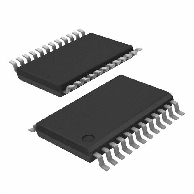
IDTCSP2510C
3.3V PHASE-LOCK LOOP CLOCK DRIVER
0ºC TO 85ºC TEMPERATURE RANGE
IDTCSP2510C
3.3V PHASE-LOCK LOOP
CLOCK DRIVER
ZERO DELAY BUFFER
FEATURES:
DESCRIPTION:
• Phase-Lock Loop Clock Distribution for Synchronous DRAM
Applications
• Distributes one clock input to one bank of ten outputs
• Output enable bank control
• External feedback (FBIN) pin is used to synchronize the
outputs to the clock input signal
• No external RC network required for PLL loop stability
• Operates at 3.3V VDD
• tpd Phase Error at 133MHz: < ±150ps
• Jitter (peak-to-peak) at 133MHz: < ±75ps @ 133MHz
• Spread Spectrum Compatible
• Operating frequency 25MHz to 140MHz
• Available in 24-Pin TSSOP package
The CSP2510C is a high performance, low-skew, low-jitter, phase-lock
loop (PLL) clock driver. It uses a PLL to precisely align, in both frequency
and phase, the feedback (FBOUT) output to the clock (CLK) input signal.
It is specifically designed for use with synchronous DRAMs. The CSP2510C
operates at 3.3V.
One bank of ten outputs provide low-skew, low-jitter copies of CLK.
Output signal duty cycles are adjusted to 50 percent, independent of the
duty cycle at CLK. The outputs can be enabled or disabled via the control
G input. When the G input is high, the outputs switch in phase and frequency
with CLK; when the G input is low, the outputs are disabled to the logic-low
state.
Unlike many products containing PLLs, the CSP2510C does not require
external RC networks. The loop filter for the PLL is included on-chip,
minimizing component count, board space, and cost.
Because it is based on PLL circuitry, the CSP2510C requires a
stabilization time to achieve phase lock of the feedback signal to the
reference signal. This stabilization time is required, following power up and
application of a fixed-frequency, fixed-phase signal at CLK, as well as
following any changes to the PLL reference or feedback signals. The PLL
can be bypassed for the test purposes by strapping AVDD to ground.
The CSP2510C is specified for operation from 0°C to +85°C. This
device is also available (on special order) in Industrial temperature range
(-40°C to +85°C). See ordering information for details.
APPLICATIONS:
• SDRAM Modules
• PC Motherboards
• Workstations
FUNCTIONAL BLOCK DIAGRAM
11
G
3
Y0
4
Y1
5
Y2
8
Y3
9
Y4
15
Y5
16
Y6
17
CLK
24
Y7
PLL
20
13
Y8
FBIN
21
AV DD
Y9
23
12
FBOUT
0ººC TO 85ººC TEMPERATURE RANGE
c
2008
NOVEMBER 2008
1
Integrated Device Technology, Inc.
DSC-5180/4
�IDTCSP2510C
3.3V PHASE-LOCK LOOP CLOCK DRIVER
0ºC TO 85ºC TEMPERATURE RANGE
PIN CONFIGURATION
ABSOLUTE MAXIMUM RATINGS(1)
AGND
1
24
CLK
VDD
2
23
AVDD
Y0
3
22
VDD
Y1
4
21
Y9
Symbol
Rating
VDD
Supply Voltage Range
–0.5 to +4.6
V
VI(1)
VO(1,2)
Input Voltage Range
Voltage range applied to any
–0.5 to +6.5
–0.5 to VDD + 0.5
V
V
IIK
output in the high or low state
Input clamp current
–50
mA
(VI
很抱歉,暂时无法提供与“CSP2510CPGG8”相匹配的价格&库存,您可以联系我们找货
免费人工找货