To our customers,
Old Company Name in Catalogs and Other Documents
On April 1st, 2010, NEC Electronics Corporation merged with Renesas Technology
Corporation, and Renesas Electronics Corporation took over all the business of both
companies. Therefore, although the old company name remains in this document, it is a valid
Renesas Electronics document. We appreciate your understanding.
Renesas Electronics website: http://www.renesas.com
April 1st, 2010
Renesas Electronics Corporation
Issued by: Renesas Electronics Corporation (http://www.renesas.com)
Send any inquiries to http://www.renesas.com/inquiry.
�Notice
1.
2.
3.
4.
5.
6.
7.
All information included in this document is current as of the date this document is issued. Such information, however, is
subject to change without any prior notice. Before purchasing or using any Renesas Electronics products listed herein, please
confirm the latest product information with a Renesas Electronics sales office. Also, please pay regular and careful attention to
additional and different information to be disclosed by Renesas Electronics such as that disclosed through our website.
Renesas Electronics does not assume any liability for infringement of patents, copyrights, or other intellectual property rights
of third parties by or arising from the use of Renesas Electronics products or technical information described in this document.
No license, express, implied or otherwise, is granted hereby under any patents, copyrights or other intellectual property rights
of Renesas Electronics or others.
You should not alter, modify, copy, or otherwise misappropriate any Renesas Electronics product, whether in whole or in part.
Descriptions of circuits, software and other related information in this document are provided only to illustrate the operation of
semiconductor products and application examples. You are fully responsible for the incorporation of these circuits, software,
and information in the design of your equipment. Renesas Electronics assumes no responsibility for any losses incurred by
you or third parties arising from the use of these circuits, software, or information.
When exporting the products or technology described in this document, you should comply with the applicable export control
laws and regulations and follow the procedures required by such laws and regulations. You should not use Renesas
Electronics products or the technology described in this document for any purpose relating to military applications or use by
the military, including but not limited to the development of weapons of mass destruction. Renesas Electronics products and
technology may not be used for or incorporated into any products or systems whose manufacture, use, or sale is prohibited
under any applicable domestic or foreign laws or regulations.
Renesas Electronics has used reasonable care in preparing the information included in this document, but Renesas Electronics
does not warrant that such information is error free. Renesas Electronics assumes no liability whatsoever for any damages
incurred by you resulting from errors in or omissions from the information included herein.
Renesas Electronics products are classified according to the following three quality grades: “Standard”, “High Quality”, and
“Specific”. The recommended applications for each Renesas Electronics product depends on the product’s quality grade, as
indicated below. You must check the quality grade of each Renesas Electronics product before using it in a particular
application. You may not use any Renesas Electronics product for any application categorized as “Specific” without the prior
written consent of Renesas Electronics. Further, you may not use any Renesas Electronics product for any application for
which it is not intended without the prior written consent of Renesas Electronics. Renesas Electronics shall not be in any way
liable for any damages or losses incurred by you or third parties arising from the use of any Renesas Electronics product for an
application categorized as “Specific” or for which the product is not intended where you have failed to obtain the prior written
consent of Renesas Electronics. The quality grade of each Renesas Electronics product is “Standard” unless otherwise
expressly specified in a Renesas Electronics data sheets or data books, etc.
“Standard”:
8.
9.
10.
11.
12.
Computers; office equipment; communications equipment; test and measurement equipment; audio and visual
equipment; home electronic appliances; machine tools; personal electronic equipment; and industrial robots.
“High Quality”: Transportation equipment (automobiles, trains, ships, etc.); traffic control systems; anti-disaster systems; anticrime systems; safety equipment; and medical equipment not specifically designed for life support.
“Specific”:
Aircraft; aerospace equipment; submersible repeaters; nuclear reactor control systems; medical equipment or
systems for life support (e.g. artificial life support devices or systems), surgical implantations, or healthcare
intervention (e.g. excision, etc.), and any other applications or purposes that pose a direct threat to human life.
You should use the Renesas Electronics products described in this document within the range specified by Renesas Electronics,
especially with respect to the maximum rating, operating supply voltage range, movement power voltage range, heat radiation
characteristics, installation and other product characteristics. Renesas Electronics shall have no liability for malfunctions or
damages arising out of the use of Renesas Electronics products beyond such specified ranges.
Although Renesas Electronics endeavors to improve the quality and reliability of its products, semiconductor products have
specific characteristics such as the occurrence of failure at a certain rate and malfunctions under certain use conditions. Further,
Renesas Electronics products are not subject to radiation resistance design. Please be sure to implement safety measures to
guard them against the possibility of physical injury, and injury or damage caused by fire in the event of the failure of a
Renesas Electronics product, such as safety design for hardware and software including but not limited to redundancy, fire
control and malfunction prevention, appropriate treatment for aging degradation or any other appropriate measures. Because
the evaluation of microcomputer software alone is very difficult, please evaluate the safety of the final products or system
manufactured by you.
Please contact a Renesas Electronics sales office for details as to environmental matters such as the environmental
compatibility of each Renesas Electronics product. Please use Renesas Electronics products in compliance with all applicable
laws and regulations that regulate the inclusion or use of controlled substances, including without limitation, the EU RoHS
Directive. Renesas Electronics assumes no liability for damages or losses occurring as a result of your noncompliance with
applicable laws and regulations.
This document may not be reproduced or duplicated, in any form, in whole or in part, without prior written consent of Renesas
Electronics.
Please contact a Renesas Electronics sales office if you have any questions regarding the information contained in this
document or Renesas Electronics products, or if you have any other inquiries.
(Note 1) “Renesas Electronics” as used in this document means Renesas Electronics Corporation and also includes its majorityowned subsidiaries.
(Note 2) “Renesas Electronics product(s)” means any product developed or manufactured by or for Renesas Electronics.
�User’s Manual
16
The revision list can be viewed directly by
clicking the title page.
The revision list summarizes the locations of
revisions and additions. Details should always
be checked by referring to the relevant text.
H8S/2138 Group, H8S/2134 Group,
H8S/2138F-ZTAT™, H8S/2134F-ZTAT™,
H8S/2132F-ZTAT™
Hardware Manual
Renesas 16-Bit Single-Chip Microcomputer
H8S Family/H8S/2100 Series
H8S/2138
H8S/2137
HD6432138S
HD6432138SW
HD64F2138
HD64F2138V
HD64F2138A
HD64F2138AV
HD6432137S
HD6432137SW
H8S/2134
H8S/2133
H8S/2132
H8S/2130
HD6432134S
HD64F2134
HD64F2134V
HD64F2134A
HD64F2134AV
HD6432133S
HD6432132
HD64F2132R
HD64F2132RV
HD6432130
Rev.4.00 2006.06
�Keep safety first in your circuit designs!
1. Renesas Technology Corp. puts the maximum effort into making semiconductor products better and
more reliable, but there is always the possibility that trouble may occur with them. Trouble with
semiconductors may lead to personal injury, fire or property damage.
Remember to give due consideration to safety when making your circuit designs, with appropriate
measures such as (i) placement of substitutive, auxiliary circuits, (ii) use of nonflammable material or
(iii) prevention against any malfunction or mishap.
Notes regarding these materials
1. These materials are intended as a reference to assist our customers in the selection of the Renesas
Technology Corp. product best suited to the customer's application; they do not convey any license
under any intellectual property rights, or any other rights, belonging to Renesas Technology Corp. or
a third party.
2. Renesas Technology Corp. assumes no responsibility for any damage, or infringement of any thirdparty's rights, originating in the use of any product data, diagrams, charts, programs, algorithms, or
circuit application examples contained in these materials.
3. All information contained in these materials, including product data, diagrams, charts, programs and
algorithms represents information on products at the time of publication of these materials, and are
subject to change by Renesas Technology Corp. without notice due to product improvements or
other reasons. It is therefore recommended that customers contact Renesas Technology Corp. or
an authorized Renesas Technology Corp. product distributor for the latest product information
before purchasing a product listed herein.
The information described here may contain technical inaccuracies or typographical errors.
Renesas Technology Corp. assumes no responsibility for any damage, liability, or other loss rising
from these inaccuracies or errors.
Please also pay attention to information published by Renesas Technology Corp. by various means,
including the Renesas Technology Corp. Semiconductor home page (http://www.renesas.com).
4. When using any or all of the information contained in these materials, including product data,
diagrams, charts, programs, and algorithms, please be sure to evaluate all information as a total
system before making a final decision on the applicability of the information and products. Renesas
Technology Corp. assumes no responsibility for any damage, liability or other loss resulting from the
information contained herein.
5. Renesas Technology Corp. semiconductors are not designed or manufactured for use in a device or
system that is used under circumstances in which human life is potentially at stake. Please contact
Renesas Technology Corp. or an authorized Renesas Technology Corp. product distributor when
considering the use of a product contained herein for any specific purposes, such as apparatus or
systems for transportation, vehicular, medical, aerospace, nuclear, or undersea repeater use.
6. The prior written approval of Renesas Technology Corp. is necessary to reprint or reproduce in
whole or in part these materials.
7. If these products or technologies are subject to the Japanese export control restrictions, they must
be exported under a license from the Japanese government and cannot be imported into a country
other than the approved destination.
Any diversion or reexport contrary to the export control laws and regulations of Japan and/or the
country of destination is prohibited.
8. Please contact Renesas Technology Corp. for further details on these materials or the products
contained therein.
Rev. 4.00 Jun 06, 2006 page ii of liv
�General Precautions on Handling of Product
1. Treatment of NC Pins
Note: Do not connect anything to the NC pins.
The NC (not connected) pins are either not connected to any of the internal circuitry or are
used as test pins or to reduce noise. If something is connected to the NC pins, the
operation of the LSI is not guaranteed.
2. Treatment of Unused Input Pins
Note: Fix all unused input pins to high or low level.
Generally, the input pins of CMOS products are high-impedance input pins. If unused pins
are in their open states, intermediate levels are induced by noise in the vicinity, a passthrough current flows internally, and a malfunction may occur.
3. Processing before Initialization
Note: When power is first supplied, the product’s state is undefined.
The states of internal circuits are undefined until full power is supplied throughout the
chip and a low level is input on the reset pin. During the period where the states are
undefined, the register settings and the output state of each pin are also undefined. Design
your system so that it does not malfunction because of processing while it is in this
undefined state. For those products which have a reset function, reset the LSI immediately
after the power supply has been turned on.
4. Prohibition of Access to Undefined or Reserved Addresses
Note: Access to undefined or reserved addresses is prohibited.
The undefined or reserved addresses may be used to expand functions, or test registers
may have been be allocated to these addresses. Do not access these registers; the system’s
operation is not guaranteed if they are accessed.
Rev. 4.00 Jun 06, 2006 page iii of liv
�Configuration of This Manual
This manual comprises the following items:
1. General Precautions on Handling of Product
2. Configuration of This Manual
3. Preface
4. Main Revisions for This Edition
The list of revisions is a summary of points that have been revised or added to earlier versions.
This does not include all of the revised contents. For details, see the actual locations in this
manual.
5. Contents
6 Overview
7. Description of Functional Modules
•
CPU and System-Control Modules
•
On-Chip Peripheral Modules
The configuration of the functional description of each module differs according to the
module. However, the generic style includes the following items:
i) Feature
ii) Input/Output Pin
iii) Register Description
iv) Operation
v) Usage Note
When designing an application system that includes this LSI, take notes into account. Each section
includes notes in relation to the descriptions given, and usage notes are given, as required, as the
final part of each section.
8. List of Registers
9. Electrical Characteristics
10. Appendix
Rev. 4.00 Jun 06, 2006 page iv of liv
�Preface
The H8S/2138 Group and H8S/2134 Group comprise high-performance microcomputers with a
32-bit H8S/2000 CPU core, and a set of on-chip supporting functions required for system
configuration.
The H8S/2000 CPU can execute basic instructions in one state, and is provided with sixteen
internal 16-bit general registers with a 32-bit configuration, and a concise and optimized
instruction set. The CPU can handle a 16-Mbyte linear address space (architecturally 4 Gbytes).
Programs based on the high-level language C can also be run efficiently.
Single-power-supply flash memory (F-ZTAT™*) and mask ROM versions are available,
providing a quick and flexible response to conditions from ramp-up through full-scale volume
production, even for applications with frequently changing specifications.
On-chip peripheral functions include a 16-bit free-running timer (FRT), 8-bit timer (TMR),
watchdog timer (WDT), two PWM timers (PWM and PWMX), a serial communication interface
(SCI, IrDA), host interface (HIF), D/A converter (DAC), A/D converter (ADC), and I/O ports. An
2
I C bus interface (IIC) can also be incorporated as an option.
An on-chip data transfer controller (DTC) is also provided, enabling high-speed data transfer
without CPU intervention.
The H8S/2138 Group has all the above on-chip supporting functions, and can also be provided
with an IIC module as an option. The H8S/2134 Group comprises reduced-function versions, with
fewer TMR channels, and no PWM, HIF, IIC, or DTC modules.
Use of the H8S/2138 or H8S/2134 Group enables compact, high-performance systems to be
implemented easily. The comprehensive PC-related interface functions and 16 × 8 matrix key-scan
functions are ideal for applications such as notebook PC keyboard control and intelligent battery
and power supply control, while the various timer functions and their interconnectability (timer
2
connection), plus the interlinked operation of the I C bus interface and data transfer controller
(DTC), in particular, make these devices ideal for use in PC monitors. In addition, the combination
of F-ZTAT™* and reduced-function versions is ideal for applications such as system units in
which on-chip program memory is essential to meet performance requirements, product start-up
times are short, and program modifications may be necessary after end-product assembly.
This manual describes the hardware of the H8S/2138 Group and H8S/2134 Group. Refer to the
H8S/2600 Series and H8S/2000 Series Software Manual for a detailed description of the
instruction set.
Note: * F-ZTAT (Flexible-ZTAT) is a trademark of Renesas Technology Corp.
Rev. 4.00 Jun 06, 2006 page v of liv
�On-Chip Supporting Modules
Group
H8S/2138 Group
H8S/2134 Group
Product names
H8S/2138, 2137
H8S/2134, 2133, 2132,
2130
Bus controller (BSC)
Available (8 bits)
Available (8 bits)
Data transfer controller (DTC)
Available
—
8-bit PWM timer (PWM)
×16
—
14-bit PWM timer (PWMX)
×2
×2
16-bit free-running timer (FRT)
×1
×1
8-bit timer (TMR)
×4
×3
Timer connection
Available
—
Watchdog timer (WDT)
×2
×2
Serial communication interface (SCI)
×3
×3
I C bus interface (IIC)
×2 (option)
—
Host interface (HIF)
×2
—
D/A converter
×2
×2
A/D converter
×8 (analog input)
×8 (analog input)
2
×8
×8
(expansion A/D inputs) (expansion A/D inputs)
Rev. 4.00 Jun 06, 2006 page vi of liv
�Main Revisions for This Edition
Item
Page
Revision (See Manual for Details)
All
—
• Notification of change in company name amended
(Before) Hitachi, Ltd. → (After) Renesas Technology Corp.
• Product naming convention amended
(Before) H8S/2138 Series → (After) H8S/2138 Group
(Before) H8S/2134 Series → (After) H8S/2134 Group
Description amended
(Before) Serial/timer control register → (After) Serial timer
control register
1.3.2 Pin Functions in
Each Operating Mode
12
Pin Name
Pin No.
Table 1.2 H8S/2138
Group Pin Functions in
Each Operating Mode
2.6.1 Overview
Table 2.1 Instruction
Classification
Table amended
FP-80A
TFP-80C
28
42
Expanded Modes
Single-Chip Modes
Mode 1
Mode 2 (EXPE = 1)
Mode 3 (EXPE = 1)
Mode 2 (EXPE = 0)
Mode 3 (EXPE = 0)
P67/TMOX/CIN7/
KIN7/IRQ7
P67/TMOX/CIN7/
KIN7/IRQ7
P67/TMOX/CIN7/
KIN7/IRQ7
Flash Memory
Programmer
Mode
VSS
Table amended
Function
Instructions
Size
Types
Arithmetic
operations
ADD, SUB, CMP, NEG
BWL
19
ADDX, SUBX, DAA, DAS
B
INC, DEC
BWL
Rev. 4.00 Jun 06, 2006 page vii of liv
�Item
Page
Revision (See Manual for Details)
9.3.1 Correspondence
between PWM Data
Register Contents and
Output Waveform
251
Table amended
Upper 4 Bits
0000
Basic Pulse Waveform (Internal)
0 1 2 3 4 5 6 7 8 9 A B C D E F 0
0001
Table 9.4 Duty Cycle
of Basic Pulse
0010
0011
0100
0101
0110
0111
..
.
1000
1001
1010
1011
1100
1101
1110
1111
10.1.3 Pin configuration 255
Channel deleted
Table 10.1 Input and
Output Pins
12.1 Overview
305
Description amended
The H8S/2138 Series also has two similar 8-bit timer channels
(TMRX and TMRY). These channels can be used in a
connected configuration using the timer connection function.
TMRX and TMRY have greater input/output and interrupt
function related restrictions than TMR0 and TMR1.
TMRX has a built-in H8S/2138, but does not have a built-in
H8S/2134.
Rev. 4.00 Jun 06, 2006 page viii of liv
�Item
Page
Revision (See Manual for Details)
16.4 Usage Notes
514 to
521
• Notes on WAIT Function
• Notes on ICDR Reads and ICCR Access in Slave Transmit
Mode
• Notes on TRS Bit Setting in Slave Mode
• Notes on Notes on Arbitration Lost in Master Mode
• Notes on Interrupt Occurrence after ACKB Reception
Description added
17.1.3 Input and Output 525
Pins
Table 17.1 Host
Interface Input/Output
Pins
19.4.3 Input Sampling
and A/D Conversion
Time
566
Note * amended
Note: * Selection of CS2 or ECS2 is by means of the CS2E
bit in SYSCR and ...
Figure 19.5 amended
(1)
φ
Figure 19.5 A/D
Conversion Timing
Address
(2)
Write signal
Input sampling
timing
ADF
tD
tSPL
tCONV
19.6 Usage Notes
572
Note added
Note: Values are reference values.
Figure 19.11 Example
of Analog Input Circuit
21.5.2 Flash Memory
Control Register 2
(FLMCR2)
590
21.6.1 Boot Mode
597
Description amended
Bits 6 to 2Reserved: Always write 0 when writing to these
bits.
Description amended
... H'(FF)E080 to H'(FF)EFFF (3968 bytes) in the 128-kbyte
versions including H8S/2132, except for H8S/2132R or
H'(FF)E880 to H'(FF)EFFF (1920 bytes) in the 64-kbyte
versions including H8S/2132R, except for H8S/2132.
Rev. 4.00 Jun 06, 2006 page ix of liv
�Item
Page
Revision (See Manual for Details)
21.6.1 Boot Mode
597
Figure 21.10 amended
1
Programming control* program area (3,968 bytes)
Figure 21.10 RAM
Areas in Boot Mode
Boot program area* (128 bytes)
2
(a) 128-kbyte versions (including H8S/2132)
(b) 64-kbyte versions (except for H8S/2132)
Note 1 added
Note: 1. In H8S/2132 F-ZTAT (Mask ROM version),
H'(FF)E080 to H'(FF)E87F is a reserved area that is used only
for boot mode operation. Do not use this area for other
purpose.
598
Description amended
· Before branching to the programming control program (RAM
area H'(FF)E080 (128-kbyte versions including H8S/2132,
except for H8S/2132R or H'(FF)E880 (64-kbyte versions,
including H8S/2132R, except for H8S/2132)), ...
22.4.5 Register
Configuration
632
Table 22.4 amended
3
3
(Before) * → (After) R/W*
23.7 Subclock Input
Circuit
678
"Note on Subclock Usage" description added
24.1 Overview
682
Table 24.1 amended
Table 22.4 Flash
Memory Registers
Table 24.1 H8S/2138
Group and H8S/2134
Group Internal States in
Each Mode
Function
On-chip
RAM
supporting
module
I/O
operation
HighSpeed
MediumSpeed
Sleep
Software
Subactive Subsleep Standby
Hardware
Standby
Functioning
Functioning
Function- Functioning (DTC) ing
Retained
Functioning
Retained
Retained
Retained
Functioning
Functioning
Functioning
Retained
Functioning
Functioning
Retained
High
impedance
24.12 Usage Notes
702
Section 24.12 added
25.2.2 DC
Characteristics
709
Note *4 amended
Module
Stop
Functioning
Watch
Note: 4. P52/SCK0/SCL0 and P97/SDA0 are NMOS push-pull
outputs in H8S/2138. ... P52/SCK0 and P97 (ICE = 0) high
levels are driven by NMOS in H8S/2138.
Table 25.3 DC
Characteristics (1)
Table 25.3 DC
Characteristics (2)
712
Table 25.3 DC
Characteristics (3)
715
Note *4 amended
Note: 4. P52/SCK0/SCL0 and P97/SDA0 are NMOS push-pull
outputs in H8S/2138. ... P52/SCK0 and P97 (ICE = 0) high
levels are driven by NMOS in H8S/2138.
Note *4 amended
Note: 4. P52/SCK0/SCL0 and P97/SDA0 are NMOS push-pull
outputs in H8S/2138. ... P52/SCK0 and P97 (ICE = 0) high
levels are driven by NMOS in H8S/2138.
Rev. 4.00 Jun 06, 2006 page x of liv
�Item
Page
Revision (See Manual for Details)
25.2.7 Usage Note
732
Description amended
Figure 25.3 Connection
of External Capacitor
(Mask ROM Type
Incorporating Step-Down
Circuit and Product Not
Incorporating Step-Down
Circuit)
25.3.2 DC
Characteristics
HD6432138S, HD6432138SW, HD6432137S,
HD6432137SW, HD6432134S, HD6432133S, HD64F2138A,
HD64F2134A
735
Table 25.16 DC
Characteristics (1)
736
Table 25.16 (1) amended
Item
Symbol
Min
Typ
Max
Test
Unit Conditions
Output high All output pins
voltage
(except P97, and
4
5
P52* )*
4
P97, P52*
VOH
VCC –0.5
—
—
V
IOH = –200 µA
3.5
—
—
V
IOH = –1 mA
2.0
—
—
V
IOH = –200 µA,
VCC = 4.5 to
5.5 V
Note *4 amended
Note: 4. P52/SCK0/SCL0 and P97/SDA0 are NMOS push-pull
outputs in H8S/2138. ... P52/SCK0 and P97 (ICE = 0) high
levels are driven by NMOS in H8S/2138.
Table 25.16 DC
Characteristics (2)
738
Table 25.16 (2) amended
Item
Symbol
Min
Typ
Max
Test
Unit Conditions
Output high All output pins
voltage
(except P97, and
4
5
P52* )*
VOH
VCC –0.5
—
—
V
IOH = –200 µA
3.5
—
—
V
IOH = –1 mA,
VCC=
4.5 V to 5.5 V
3.0
—
—
V
IOH = –1 mA,
VCC < 4.5 V
1.5
—
—
V
IOH = –200 µA,
VCC = 4.0 to
5.5 V
4
P97, P52*
739
Note *4 amended
Note: 4. P52/SCK0/SCL0 and P97/SDA0 are NMOS push-pull
outputs in H8S/2138. ... P52/SCK0 and P97 (ICE = 0) high
levels are driven by NMOS in H8S/2138.
Rev. 4.00 Jun 06, 2006 page xi of liv
�Item
Page
Revision (See Manual for Details)
25.3.2 DC
Characteristics
740
Table 25.16 (3) amended
Table 25.16 DC
Characteristics (3)
Item
Symbol
Min
Typ Max
Test
Unit Conditions
Output high All output pins
(except P97, and
voltage
4
5
P52* )*
VOH
VCC –0.5
—
—
V
IOH = –200 µA
VCC –1.0
—
—
V
IOH = –1 mA
0.5
—
—
V
IOH = –200 µA,
VCC = 2.7 to
3.5 V
P97, P52*
742
4
Note *4 amended
Note: 4. P52/SCK0/SCL0 and P97/SDA0 are NMOS push-pull
outputs in H8S/2138. ... P52/SCK0 and P97 (ICE = 0) high
levels are driven by NMOS in H8S/2138.
25.3.6 Flash Memory
Characteristics
756
Table 25.27 amended
Item
Table 25.27 Flash
Memory Characteristics
(Programming/Erasing
Operating Range)
Reprogramming count
Data retention time*10
757
Symbol Min
100*8
Typ
Max
10000*9 —
Unit
tDRP
—
Years
NWEC
10
—
Test
Condition
Times
Notes 8 to 10 added
Notes: 8. Minimum number of times for which all
characteristics are guaranteed after rewriting (Guarantee
range is 1 to minimum value).
9. Reference value for 25C° (as a guide line, rewriting should
normally function up to this value).
10. Data retention characteristics when rewriting is performed
within the specification range, including the minimum value.
25.4.2 DC
Characteristics
761
Table 25.29 (1) amended
Item
Table 25.29 DC
Characteristics (1)
Three-state
leakage
current
(off state)
Ports 1 to 6, 8, 9
Input pull-up Ports 1 to 3
MOS current
Port 6
Table 25.29 DC
Characteristics (3)
766
Table 25.40 DC
Characteristics (1)
782
Typ
Max
Test
Unit Conditions
ITSI
—
—
1.0
µA
Vin = 0.5 to
VCC –0.5 V
–IP
50
—
300
µA
60
—
500
µA
Vin = 0 V, VCC
= 5 V ±10%
Note *5 added to test conditions for input pull-up MOS current
5
V = 0 V, V = 2.7 V* to 3.6 V
in
25.5.2 DC
Characteristics
Symbol Min
CC
Table 25.40 (1) amended
Item
Input
pull-up
MOS
current
Rev. 4.00 Jun 06, 2006 page xii of liv
Ports 1 to 3
Port 6
Symbol
Min
Typ
Max
Test
Unit Conditions
–IP
30
—
300
µA
60
—
600
µA
Vin = 0 V, VCC
= 5 V ±10%
�Item
Page
Revision (See Manual for Details)
25.5.6 Flash Memory
Characteristics
797
Table 25.49 amended
Item
Table 25.49 Flash
Memory Characteristics
(Programming/Erasing
Operating Range)
Reprogramming count
Data retention time*10
798
Symbol Min
100*8
Typ
Max
10000*9 —
Times
tDRP
—
Years
NWEC
10
—
Unit
Test
Condition
Notes 8 to 10 added
Notes: 8. Minimum number of times for which all
characteristics are guaranteed after rewriting (Guarantee
range is 1 to minimum value).
9. Reference value for 25C° (as a guide line, rewriting should
normally function up to this value).
10. Data retention characteristics when rewriting is performed
within the specification range, including the minimum value.
B.3 Function
906
SYSCR2 H'FF83 HIF
Figure amended
Bit
7
6
5
4
3
2
1
0
KWUL1
KWUL0
P6PUE
—
SDE
CS4E
CS3E
HI12E
Initial value
0
0
0
0
0
0
0
0
Read/Write
R/W
R/W
R/W
—
R/W
R/W
R/W
R/W
Host interface enable
0
Host interface function
disabled
1
Host interface function
enabled
CS3 enable
0
Host interface pin channel 3
functions disabled
1
Host interface pin channel 3
functions enabled
CS4 enable
907
0
Host interface pin channel 4
functions disabled
1
Host interface pin channel 4
functions enabled
EBR1, 2 H'FF82, H'FF83 Flash memory
Note *2 amended
Note: 2. Bits EB8 and EB9 are not present in the 64-kbyte
versions; these bits cannot be modified and are always read
as 0.
Rev. 4.00 Jun 06, 2006 page xiii of liv
�Item
Page
Revision (See Manual for Details)
B.3 Function
938
STCR H'FFC3 System
Figure amended
Bit
7
6
5
4
3
2
1
0
—
IICX1
IICX0
IICE
FLSHE
—
ICKS1
ICKS0
Initial value
0
0
0
0
0
0
0
0
Read/Write
R/W
R/W
R/W
R/W
R/W
R/W
R/W
R/W
Internal Clock Source
Select 1 and 0*1
Reserved
Flash memory control register enable
I2C
0
Flash memory control register not selected
1
Flash memory control register selected
master enable
0
CPU access to SCI0, SCI1, and SCI2 control
registers is enabled
1
CPU access to I2C bus interface data, PWMX data
registers and control registers is enabled
I2C transfer select 1 and 0*2
Reserved
939
SYSCR H'FFC4 System
Figure amended
Bit
7
6
5
4
3
2
1
0
CS2E
IOSE
INTM1
INTM0
XRST
NMIEG
HIE
RAME
Initial value
0
0
0
0
1
0
0
1
Read/Write
R/W
R/W
R
R/W
R
R/W
R/W
R/W
RAM Enable
0
On-chip RAM is disabled
1
On-chip RAM is enabled
Host interface enable
0 Addresses H'(FF)FFF0 to H'(FF)FFF7
and H'(FF)FFFC to H'(FF)FFFF are
used for access to 8-bit timer (channel
X and Y) data registers and control
registers, and timer connection
control registers
1
Addresses H'(FF)FFF0 to H'(FF)FFF7
and H'(FF)FFFC to H'(FF)FFFF are
used for access to host interface data
registers and control registers, and
keyboard controller and MOS input
pull-up control registers
NMI edge select
0
Falling edge
1
Rising edge
External reset
0
Reset generated by watchdog timer overflow
1
Reset generated by an external reset
Interrupt control selection mode 1 and 0
Bit 5
Bit 4
Interrupt
INTM1 INTM0 control mode
0
1
Rev. 4.00 Jun 06, 2006 page xiv of liv
Description
0
0
Interrupts controlled by I bit
1
1
Interrupts controlled by I and UI bits, and ICR
(Initial value)
0
2
Cannot be used in the LSI
1
3
Cannot be used in the LSI
�Item
Page
Revision (See Manual for Details)
B.3 Function
942
WSCR H'FFC7 Bus Controller
Figure amended
7
6
RAMS
RAM0
Bit
Initial value
0
0
Read/Write
R/W
R/W
Reserved
Note: Always write 0
when writing to
these bits in
the A-mask
version.
959
STR1, 2 H'FFF6, H'FFFE HIF
Figure amended
Bit
1
0
IBF
OBF
Initial value
0
0
Slave R/W
R
R/(W)
Host R/W
R
R
Output data register full
0
[Clearing condition]
When the host processor
reads ODR or the slave
writes 0 in the OBF bit
1
[Setting condition]
When the slave processor
writes to ODR
Input data register full
0
[Clearing condition]
When the slave processor reads IDR
1
[Setting condition]
When the host processor writes to IDR
Rev. 4.00 Jun 06, 2006 page xv of liv
�Item
Page
Revision (See Manual for Details)
Appendix G Package
Dimensions
1002
Figure replaced
1003
Figure replaced
Figure G.1 Package
Dimensions (FP-80A)
Figure G.2 Package
Dimensions (TFP-80C)
Rev. 4.00 Jun 06, 2006 page xvi of liv
�Contents
Section 1 Overview .............................................................................................................
1.1
1.2
1.3
1
Overview........................................................................................................................... 1
Internal Block Diagram..................................................................................................... 7
Pin Arrangement and Functions........................................................................................ 9
1.3.1 Pin Arrangement .................................................................................................. 9
1.3.2 Pin Functions in Each Operating Mode ............................................................... 11
1.3.3 Pin Functions ....................................................................................................... 18
Section 2 CPU ...................................................................................................................... 25
2.1
2.2
2.3
2.4
2.5
2.6
2.7
2.8
Overview...........................................................................................................................
2.1.1 Features................................................................................................................
2.1.2 Differences between H8S/2600 CPU and H8S/2000 CPU ..................................
2.1.3 Differences from H8/300 CPU ............................................................................
2.1.4 Differences from H8/300H CPU..........................................................................
CPU Operating Modes ......................................................................................................
Address Space...................................................................................................................
Register Configuration......................................................................................................
2.4.1 Overview..............................................................................................................
2.4.2 General Registers .................................................................................................
2.4.3 Control Registers .................................................................................................
2.4.4 Initial Register Values..........................................................................................
Data Formats.....................................................................................................................
2.5.1 General Register Data Formats ............................................................................
2.5.2 Memory Data Formats .........................................................................................
Instruction Set ...................................................................................................................
2.6.1 Overview..............................................................................................................
2.6.2 Instructions and Addressing Modes .....................................................................
2.6.3 Table of Instructions Classified by Function .......................................................
2.6.4 Basic Instruction Formats ....................................................................................
2.6.5 Notes on Use of Bit-Manipulation Instructions ...................................................
Addressing Modes and Effective Address Calculation .....................................................
2.7.1 Addressing Mode.................................................................................................
2.7.2 Effective Address Calculation .............................................................................
Processing States...............................................................................................................
2.8.1 Overview..............................................................................................................
2.8.2 Reset State............................................................................................................
2.8.3 Exception-Handling State ....................................................................................
2.8.4 Program Execution State......................................................................................
25
25
26
27
27
28
33
34
34
35
36
38
39
39
41
42
42
43
44
53
54
55
55
58
62
62
63
64
65
Rev. 4.00 Jun 06, 2006 page xvii of liv
�2.8.5 Bus-Released State...............................................................................................
2.8.6 Power-Down State ...............................................................................................
2.9 Basic Timing .....................................................................................................................
2.9.1 Overview..............................................................................................................
2.9.2 On-Chip Memory (ROM, RAM) .........................................................................
2.9.3 On-Chip Supporting Module Access Timing ......................................................
2.9.4 External Address Space Access Timing ..............................................................
2.10 Usage Note........................................................................................................................
2.10.1 TAS Instruction....................................................................................................
2.10.2 STM/LDM Instruction .........................................................................................
65
65
66
66
66
68
69
70
70
70
Section 3 MCU Operating Modes .................................................................................. 71
3.1
3.2
3.3
3.4
3.5
Overview...........................................................................................................................
3.1.1 Operating Mode Selection ...................................................................................
3.1.2 Register Configuration.........................................................................................
Register Descriptions ........................................................................................................
3.2.1 Mode Control Register (MDCR) .........................................................................
3.2.2 System Control Register (SYSCR) ......................................................................
3.2.3 Bus Control Register (BCR) ................................................................................
3.2.4 Serial Timer Control Register (STCR) ................................................................
Operating Mode Descriptions ...........................................................................................
3.3.1 Mode 1 .................................................................................................................
3.3.2 Mode 2 .................................................................................................................
3.3.3 Mode 3 .................................................................................................................
Pin Functions in Each Operating Mode ............................................................................
Memory Map in Each Operating Mode ............................................................................
71
71
72
72
72
73
75
76
78
78
78
78
79
79
Section 4 Exception Handling ......................................................................................... 91
4.1
4.2
4.3
4.4
4.5
4.6
Overview...........................................................................................................................
4.1.1 Exception Handling Types and Priority...............................................................
4.1.2 Exception Handling Operation.............................................................................
4.1.3 Exception Sources and Vector Table ...................................................................
Reset..................................................................................................................................
4.2.1 Overview..............................................................................................................
4.2.2 Reset Sequence ....................................................................................................
4.2.3 Interrupts after Reset............................................................................................
Interrupts ...........................................................................................................................
Trap Instruction.................................................................................................................
Stack Status after Exception Handling..............................................................................
Notes on Use of the Stack .................................................................................................
Rev. 4.00 Jun 06, 2006 page xviii of liv
91
91
92
92
94
94
94
96
97
98
99
100
�Section 5 Interrupt Controller .......................................................................................... 101
5.1
5.2
5.3
5.4
5.5
5.6
5.7
Overview...........................................................................................................................
5.1.1 Features................................................................................................................
5.1.2 Block Diagram .....................................................................................................
5.1.3 Pin Configuration.................................................................................................
5.1.4 Register Configuration.........................................................................................
Register Descriptions ........................................................................................................
5.2.1 System Control Register (SYSCR) ......................................................................
5.2.2 Interrupt Control Registers A to C (ICRA to ICRC)............................................
5.2.3 IRQ Enable Register (IER) ..................................................................................
5.2.4 IRQ Sense Control Registers H and L (ISCRH, ISCRL).....................................
5.2.5 IRQ Status Register (ISR)....................................................................................
5.2.6 Keyboard Matrix Interrupt Mask Register (KMIMR) .........................................
5.2.7 Address Break Control Register (ABRKCR).......................................................
5.2.8 Break Address Registers A, B, C (BARA, BARB, BARC).................................
Interrupt Sources...............................................................................................................
5.3.1 External Interrupts ...............................................................................................
5.3.2 Internal Interrupts.................................................................................................
5.3.3 Interrupt Exception Vector Table ........................................................................
Address Breaks .................................................................................................................
5.4.1 Features................................................................................................................
5.4.2 Block Diagram .....................................................................................................
5.4.3 Operation .............................................................................................................
5.4.4 Usage Notes .........................................................................................................
Interrupt Operation............................................................................................................
5.5.1 Interrupt Control Modes and Interrupt Operation ................................................
5.5.2 Interrupt Control Mode 0 .....................................................................................
5.5.3 Interrupt Control Mode 1 .....................................................................................
5.5.4 Interrupt Exception Handling Sequence ..............................................................
5.5.5 Interrupt Response Times ....................................................................................
Usage Notes ......................................................................................................................
5.6.1 Contention between Interrupt Generation and Disabling.....................................
5.6.2 Instructions that Disable Interrupts ......................................................................
5.6.3 Interrupts during Execution of EEPMOV Instruction..........................................
DTC Activation by Interrupt.............................................................................................
5.7.1 Overview..............................................................................................................
5.7.2 Block Diagram .....................................................................................................
5.7.3 Operation .............................................................................................................
101
101
102
102
103
104
104
105
106
106
107
109
111
112
113
113
115
115
118
118
118
119
119
121
121
124
126
129
131
132
132
133
133
134
134
134
135
Section 6 Bus Controller ................................................................................................... 137
6.1
Overview........................................................................................................................... 137
Rev. 4.00 Jun 06, 2006 page xix of liv
�6.2
6.3
6.4
6.5
6.6
6.7
6.1.1 Features................................................................................................................
6.1.2 Block Diagram .....................................................................................................
6.1.3 Pin Configuration.................................................................................................
6.1.4 Register Configuration.........................................................................................
Register Descriptions ........................................................................................................
6.2.1 Bus Control Register (BCR) ................................................................................
6.2.2 Wait State Control Register (WSCR) ..................................................................
Overview of Bus Control ..................................................................................................
6.3.1 Bus Specifications................................................................................................
6.3.2 Advanced Mode...................................................................................................
6.3.3 Normal Mode.......................................................................................................
6.3.4 I/O Select Signal ..................................................................................................
Basic Bus Interface ...........................................................................................................
6.4.1 Overview..............................................................................................................
6.4.2 Data Size and Data Alignment.............................................................................
6.4.3 Valid Strobes........................................................................................................
6.4.4 Basic Timing........................................................................................................
6.4.5 Wait Control ........................................................................................................
Burst ROM Interface.........................................................................................................
6.5.1 Overview..............................................................................................................
6.5.2 Basic Timing........................................................................................................
6.5.3 Wait Control ........................................................................................................
Idle Cycle ..........................................................................................................................
6.6.1 Operation .............................................................................................................
6.6.2 Pin States in Idle Cycle ........................................................................................
Bus Arbitration..................................................................................................................
6.7.1 Overview..............................................................................................................
6.7.2 Operation .............................................................................................................
6.7.3 Bus Transfer Timing ............................................................................................
137
138
139
139
140
140
141
143
143
144
144
145
146
146
146
147
148
151
153
153
153
155
155
155
156
157
157
157
158
Section 7 Data Transfer Controller [H8S/2138 Group]............................................ 159
7.1
7.2
Overview...........................................................................................................................
7.1.1 Features................................................................................................................
7.1.2 Block Diagram .....................................................................................................
7.1.3 Register Configuration.........................................................................................
Register Descriptions ........................................................................................................
7.2.1 DTC Mode Register A (MRA) ............................................................................
7.2.2 DTC Mode Register B (MRB).............................................................................
7.2.3 DTC Source Address Register (SAR)..................................................................
7.2.4 DTC Destination Address Register (DAR)..........................................................
7.2.5 DTC Transfer Count Register A (CRA) ..............................................................
Rev. 4.00 Jun 06, 2006 page xx of liv
159
159
160
161
162
162
164
165
165
165
�7.3
7.4
7.5
7.2.6 DTC Transfer Count Register B (CRB)...............................................................
7.2.7 DTC Enable Registers (DTCER) .........................................................................
7.2.8 DTC Vector Register (DTVECR)........................................................................
7.2.9 Module Stop Control Register (MSTPCR) ..........................................................
Operation ..........................................................................................................................
7.3.1 Overview..............................................................................................................
7.3.2 Activation Sources ...............................................................................................
7.3.3 DTC Vector Table................................................................................................
7.3.4 Location of Register Information in Address Space ............................................
7.3.5 Normal Mode.......................................................................................................
7.3.6 Repeat Mode ........................................................................................................
7.3.7 Block Transfer Mode ...........................................................................................
7.3.8 Chain Transfer .....................................................................................................
7.3.9 Operation Timing.................................................................................................
7.3.10 Number of DTC Execution States........................................................................
7.3.11 Procedures for Using the DTC.............................................................................
7.3.12 Examples of Use of the DTC ...............................................................................
Interrupts ...........................................................................................................................
Usage Notes ......................................................................................................................
166
166
167
168
169
169
171
173
175
176
177
178
180
181
182
184
185
187
187
Section 8 I/O Ports .............................................................................................................. 189
8.1
8.2
8.3
8.4
8.5
Overview...........................................................................................................................
Port 1.................................................................................................................................
8.2.1 Overview..............................................................................................................
8.2.2 Register Configuration.........................................................................................
8.2.3 Pin Functions in Each Mode ................................................................................
8.2.4 MOS Input Pull-Up Function...............................................................................
Port 2.................................................................................................................................
8.3.1 Overview..............................................................................................................
8.3.2 Register Configuration.........................................................................................
8.3.3 Pin Functions in Each Mode ................................................................................
8.3.4 MOS Input Pull-Up Function...............................................................................
Port 3.................................................................................................................................
8.4.1 Overview..............................................................................................................
8.4.2 Register Configuration.........................................................................................
8.4.3 Pin Functions in Each Mode ................................................................................
8.4.4 MOS Input Pull-Up Function...............................................................................
Port 4.................................................................................................................................
8.5.1 Overview..............................................................................................................
8.5.2 Register Configuration.........................................................................................
8.5.3 Pin Functions .......................................................................................................
189
195
195
197
199
201
201
201
203
205
207
208
208
209
211
212
213
213
213
214
Rev. 4.00 Jun 06, 2006 page xxi of liv
�8.6
Port 5.................................................................................................................................
8.6.1 Overview..............................................................................................................
8.6.2 Register Configuration.........................................................................................
8.6.3 Pin Functions .......................................................................................................
8.7 Port 6.................................................................................................................................
8.7.1 Overview..............................................................................................................
8.7.2 Register Configuration.........................................................................................
8.7.3 Pin Functions .......................................................................................................
8.7.4 MOS Input Pull-Up Function...............................................................................
8.8 Port 7.................................................................................................................................
8.8.1 Overview..............................................................................................................
8.8.2 Register Configuration.........................................................................................
8.8.3 Pin Functions .......................................................................................................
8.9 Port 8.................................................................................................................................
8.9.1 Overview..............................................................................................................
8.9.2 Register Configuration.........................................................................................
8.9.3 Pin Functions .......................................................................................................
8.10 Port 9.................................................................................................................................
8.10.1 Overview..............................................................................................................
8.10.2 Register Configuration.........................................................................................
8.10.3 Pin Functions .......................................................................................................
218
218
218
220
221
221
222
225
227
228
228
228
229
230
230
230
231
234
234
235
236
Section 9 8-Bit PWM Timers [H8S/2138 Group]...................................................... 241
9.1
9.2
9.3
Overview...........................................................................................................................
9.1.1 Features................................................................................................................
9.1.2 Block Diagram .....................................................................................................
9.1.3 Pin Configuration.................................................................................................
9.1.4 Register Configuration.........................................................................................
Register Descriptions ........................................................................................................
9.2.1 PWM Register Select (PWSL).............................................................................
9.2.2 PWM Data Registers (PWDR0 to PWDR15) ......................................................
9.2.3 PWM Data Polarity Registers A and B (PWDPRA and PWDPRB)....................
9.2.4 PWM Output Enable Registers A and B (PWOERA and PWOERB) .................
9.2.5 Peripheral Clock Select Register (PCSR) ............................................................
9.2.6 Port 1 Data Direction Register (P1DDR).............................................................
9.2.7 Port 2 Data Direction Register (P2DDR).............................................................
9.2.8 Port 1 Data Register (P1DR)................................................................................
9.2.9 Port 2 Data Register (P2DR)................................................................................
9.2.10 Module Stop Control Register (MSTPCR) ..........................................................
Operation ..........................................................................................................................
Rev. 4.00 Jun 06, 2006 page xxii of liv
241
241
242
243
243
244
244
246
246
247
248
248
249
249
249
250
251
�9.3.1
Correspondence between PWM Data Register Contents
and Output Waveform.......................................................................................... 251
Section 10 14-Bit PWM D/A ...........................................................................................
10.1 Overview...........................................................................................................................
10.1.1 Features................................................................................................................
10.1.2 Block Diagram .....................................................................................................
10.1.3 Pin Configuration.................................................................................................
10.1.4 Register Configuration.........................................................................................
10.2 Register Descriptions ........................................................................................................
10.2.1 PWM D/A Counter (DACNT) .............................................................................
10.2.2 D/A Data Registers A and B (DADRA and DADRB).........................................
10.2.3 PWM D/A Control Register (DACR) ..................................................................
10.2.4 Module Stop Control Register (MSTPCR) ..........................................................
10.3 Bus Master Interface .........................................................................................................
10.4 Operation ..........................................................................................................................
253
253
253
254
255
255
256
256
257
259
261
262
265
Section 11 16-Bit Free-Running Timer......................................................................... 269
11.1 Overview...........................................................................................................................
11.1.1 Features................................................................................................................
11.1.2 Block Diagram .....................................................................................................
11.1.3 Input and Output Pins ..........................................................................................
11.1.4 Register Configuration.........................................................................................
11.2 Register Descriptions ........................................................................................................
11.2.1 Free-Running Counter (FRC) ..............................................................................
11.2.2 Output Compare Registers A and B (OCRA, OCRB) .........................................
11.2.3 Input Capture Registers A to D (ICRA to ICRD) ................................................
11.2.4 Output Compare Registers AR and AF (OCRAR, OCRAF) ...............................
11.2.5 Output Compare Register DM (OCRDM) ...........................................................
11.2.6 Timer Interrupt Enable Register (TIER) ..............................................................
11.2.7 Timer Control/Status Register (TCSR) ................................................................
11.2.8 Timer Control Register (TCR) .............................................................................
11.2.9 Timer Output Compare Control Register (TOCR) ..............................................
11.2.10 Module Stop Control Register (MSTPCR) ..........................................................
11.3 Operation ..........................................................................................................................
11.3.1 FRC Increment Timing ........................................................................................
11.3.2 Output Compare Output Timing ..........................................................................
11.3.3 FRC Clear Timing................................................................................................
11.3.4 Input Capture Input Timing .................................................................................
11.3.5 Timing of Input Capture Flag (ICF) Setting ........................................................
11.3.6 Setting of Output Compare Flags A and B (OCFA, OCFB)................................
269
269
270
271
272
273
273
273
274
275
276
276
278
282
284
286
287
287
288
289
289
292
293
Rev. 4.00 Jun 06, 2006 page xxiii of liv
�11.3.7 Setting of FRC Overflow Flag (OVF) .................................................................
11.3.8 Automatic Addition of OCRA and OCRAR/OCRAF .........................................
11.3.9 ICRD and OCRDM Mask Signal Generation ......................................................
11.4 Interrupts ...........................................................................................................................
11.5 Sample Application...........................................................................................................
11.6 Usage Notes ......................................................................................................................
294
294
295
296
297
298
Section 12 8-Bit Timers .....................................................................................................
12.1 Overview...........................................................................................................................
12.1.1 Features................................................................................................................
12.1.2 Block Diagram .....................................................................................................
12.1.3 Pin Configuration.................................................................................................
12.1.4 Register Configuration.........................................................................................
12.2 Register Descriptions ........................................................................................................
12.2.1 Timer Counter (TCNT)........................................................................................
12.2.2 Time Constant Register A (TCORA)...................................................................
12.2.3 Time Constant Register B (TCORB) ...................................................................
12.2.4 Timer Control Register (TCR) .............................................................................
12.2.5 Timer Control/Status Register (TCSR) ................................................................
12.2.6 Serial Timer Control Register (STCR) ................................................................
12.2.7 System Control Register (SYSCR) ......................................................................
12.2.8 Timer Connection Register S (TCONRS)............................................................
12.2.9 Input Capture Register (TICR) [TMRX Additional Function] ............................
12.2.10 Time Constant Register C (TCORC) [TMRX Additional Function]...................
12.2.11 Input Capture Registers R and F (TICRR, TICRF)
[TMRX Additional Functions].............................................................................
12.2.12 Timer Input Select Register (TISR) [TMRY Additional Function].....................
12.2.13 Module Stop Control Register (MSTPCR) ..........................................................
12.3 Operation ..........................................................................................................................
12.3.1 TCNT Incrementation Timing .............................................................................
12.3.2 Compare-Match Timing.......................................................................................
12.3.3 TCNT External Reset Timing ..............................................................................
12.3.4 Timing of Overflow Flag (OVF) Setting .............................................................
12.3.5 Operation with Cascaded Connection..................................................................
12.3.6 Input Capture Operation ......................................................................................
12.4 Interrupt Sources...............................................................................................................
12.5 8-Bit Timer Application Example.....................................................................................
12.6 Usage Notes ......................................................................................................................
12.6.1 Contention between TCNT Write and Clear........................................................
12.6.2 Contention between TCNT Write and Increment ................................................
12.6.3 Contention between TCOR Write and Compare-Match ......................................
305
305
305
306
307
308
309
309
310
311
312
315
319
320
320
321
322
Rev. 4.00 Jun 06, 2006 page xxiv of liv
322
323
324
325
325
326
328
328
329
330
333
334
335
335
336
337
�12.6.4 Contention between Compare-Matches A and B................................................. 338
12.6.5 Switching of Internal Clocks and TCNT Operation............................................. 338
Section 13 Timer Connection [H8S/2138 Group]...................................................... 341
13.1 Overview...........................................................................................................................
13.1.1 Features................................................................................................................
13.1.2 Block Diagram .....................................................................................................
13.1.3 Input and Output Pins ..........................................................................................
13.1.4 Register Configuration.........................................................................................
13.2 Register Descriptions ........................................................................................................
13.2.1 Timer Connection Register I (TCONRI) .............................................................
13.2.2 Timer Connection Register O (TCONRO) ..........................................................
13.2.3 Timer Connection Register S (TCONRS)............................................................
13.2.4 Edge Sense Register (SEDGR) ............................................................................
13.2.5 Module Stop Control Register (MSTPCR) ..........................................................
13.3 Operation ..........................................................................................................................
13.3.1 PWM Decoding (PDC Signal Generation) ..........................................................
13.3.2 Clamp Waveform Generation (CL1/CL2/CL3 Signal Generation) .....................
13.3.3 Measurement of 8-Bit Timer Divided Waveform Period ....................................
13.3.4 IHI Signal and 2fH Modification .........................................................................
13.3.5 IVI Signal Fall Modification and IHI Synchronization .......................................
13.3.6 Internal Synchronization Signal Generation
(IHG/IVG/CL4 Signal Generation) .....................................................................
13.3.7 HSYNCO Output .................................................................................................
13.3.8 VSYNCO Output .................................................................................................
13.3.9 CBLANK Output .................................................................................................
341
341
342
343
344
344
344
347
349
351
354
355
355
357
358
360
362
364
367
368
369
Section 14 Watchdog Timer (WDT) .............................................................................. 371
14.1 Overview...........................................................................................................................
14.1.1 Features................................................................................................................
14.1.2 Block Diagram .....................................................................................................
14.1.3 Pin Configuration.................................................................................................
14.1.4 Register Configuration.........................................................................................
14.2 Register Descriptions ........................................................................................................
14.2.1 Timer Counter (TCNT)........................................................................................
14.2.2 Timer Control/Status Register (TCSR) ................................................................
14.2.3 System Control Register (SYSCR) ......................................................................
14.2.4 Notes on Register Access.....................................................................................
14.3 Operation ..........................................................................................................................
14.3.1 Watchdog Timer Operation .................................................................................
14.3.2 Interval Timer Operation .....................................................................................
371
371
372
374
374
375
375
376
379
380
381
381
382
Rev. 4.00 Jun 06, 2006 page xxv of liv
�14.3.3 Timing of Setting of Overflow Flag (OVF) .........................................................
14.4 Interrupts ...........................................................................................................................
14.5 Usage Notes ......................................................................................................................
14.5.1 Contention between Timer Counter (TCNT) Write and Increment .....................
14.5.2 Changing Value of CKS2 to CKS0......................................................................
14.5.3 Switching between Watchdog Timer Mode and Interval Timer Mode................
14.5.4 Counter Value in Transitions between High-Speed Mode, Subactive Mode,
and Watch Mode..................................................................................................
14.5.5 OVF Flag Clear Condition...................................................................................
383
384
384
384
385
385
385
386
Section 15 Serial Communication Interface (SCI, IrDA) ........................................
15.1 Overview...........................................................................................................................
15.1.1 Features................................................................................................................
15.1.2 Block Diagram .....................................................................................................
15.1.3 Pin Configuration.................................................................................................
15.1.4 Register Configuration.........................................................................................
15.2 Register Descriptions ........................................................................................................
15.2.1 Receive Shift Register (RSR) ..............................................................................
15.2.2 Receive Data Register (RDR) ..............................................................................
15.2.3 Transmit Shift Register (TSR) .............................................................................
15.2.4 Transmit Data Register (TDR).............................................................................
15.2.5 Serial Mode Register (SMR)................................................................................
15.2.6 Serial Control Register (SCR)..............................................................................
15.2.7 Serial Status Register (SSR) ................................................................................
15.2.8 Bit Rate Register (BRR) ......................................................................................
15.2.9 Serial Interface Mode Register (SCMR)..............................................................
15.2.10 Module Stop Control Register (MSTPCR) ..........................................................
15.2.11 Keyboard Comparator Control Register (KBCOMP) ..........................................
15.3 Operation ..........................................................................................................................
15.3.1 Overview..............................................................................................................
15.3.2 Operation in Asynchronous Mode .......................................................................
15.3.3 Multiprocessor Communication Function............................................................
15.3.4 Operation in Synchronous Mode .........................................................................
15.3.5 IrDA Operation ....................................................................................................
15.4 SCI Interrupts....................................................................................................................
15.5 Usage Notes ......................................................................................................................
387
387
387
389
390
390
392
392
392
393
393
394
397
401
405
413
414
416
417
417
419
430
438
447
450
451
Section 16 I2C Bus Interface [H8S/2138 Group Option] ......................................... 455
16.1 Overview........................................................................................................................... 455
16.1.1 Features................................................................................................................ 455
16.1.2 Block Diagram ..................................................................................................... 456
Rev. 4.00 Jun 06, 2006 page xxvi of liv
�16.1.3 Input/Output Pins .................................................................................................
16.1.4 Register Configuration.........................................................................................
16.2 Register Descriptions ........................................................................................................
2
16.2.1 I C Bus Data Register (ICDR) .............................................................................
16.2.2 Slave Address Register (SAR) .............................................................................
16.2.3 Second Slave Address Register (SARX) .............................................................
2
16.2.4 I C Bus Mode Register (ICMR) ...........................................................................
2
16.2.5 I C Bus Control Register (ICCR) .........................................................................
2
16.2.6 I C Bus Status Register (ICSR)............................................................................
16.2.7 Serial Timer Control Register (STCR) ................................................................
16.2.8 DDC Switch Register (DDCSWR) ......................................................................
16.2.9 Module Stop Control Register (MSTPCR) ..........................................................
16.3 Operation ..........................................................................................................................
2
16.3.1 I C Bus Data Format ............................................................................................
16.3.2 Master Transmit Operation ..................................................................................
16.3.3 Master Receive Operation....................................................................................
16.3.4 Slave Receive Operation......................................................................................
16.3.5 Slave Transmit Operation ....................................................................................
16.3.6 IRIC Setting Timing and SCL Control ................................................................
2
16.3.7 Automatic Switching from Formatless Mode to I C Bus Format ........................
16.3.8 Operation Using the DTC ....................................................................................
16.3.9 Noise Canceler .....................................................................................................
16.3.10 Sample Flowcharts...............................................................................................
16.3.11 Initialization of Internal State ..............................................................................
16.4 Usage Notes ......................................................................................................................
458
459
460
460
463
464
465
468
475
480
481
484
485
485
487
489
492
495
496
498
499
500
500
505
506
Section 17 Host Interface [H8S/2138 Group] ............................................................. 523
17.1 Overview...........................................................................................................................
17.1.1 Features................................................................................................................
17.1.2 Block Diagram .....................................................................................................
17.1.3 Input and Output Pins ..........................................................................................
17.1.4 Register Configuration.........................................................................................
17.2 Register Descriptions ........................................................................................................
17.2.1 System Control Register (SYSCR) ......................................................................
17.2.2 System Control Register 2 (SYSCR2) .................................................................
17.2.3 Host Interface Control Register (HICR) ..............................................................
17.2.4 Input Data Register 1 (IDR1)...............................................................................
17.2.5 Output Data Register 1 (ODR1)...........................................................................
17.2.6 Status Register 1 (STR1) .....................................................................................
17.2.7 Input Data Register 2 (IDR2)...............................................................................
17.2.8 Output Data Register 2 (ODR2)...........................................................................
523
523
524
525
526
527
527
528
529
530
530
531
532
533
Rev. 4.00 Jun 06, 2006 page xxvii of liv
�17.2.9 Status Register 2 (STR2) .....................................................................................
17.2.10 Module Stop Control Register (MSTPCR) ..........................................................
17.3 Operation ..........................................................................................................................
17.3.1 Host Interface Operation......................................................................................
17.3.2 Control States.......................................................................................................
17.3.3 A20 Gate ..............................................................................................................
17.3.4 Host Interface Pin Shutdown Function ................................................................
17.4 Interrupts ...........................................................................................................................
17.4.1 IBF1, IBF2 ...........................................................................................................
17.4.2 HIRQ11, HIRQ1, and HIRQ12............................................................................
17.5 Usage Note........................................................................................................................
533
535
536
536
536
537
539
541
541
541
542
Section 18 D/A Converter ................................................................................................. 543
18.1 Overview...........................................................................................................................
18.1.1 Features................................................................................................................
18.1.2 Block Diagram .....................................................................................................
18.1.3 Input and Output Pins ..........................................................................................
18.1.4 Register Configuration.........................................................................................
18.2 Register Descriptions ........................................................................................................
18.2.1 D/A Data Registers 0 and 1 (DADR0, DADR1) .................................................
18.2.2 D/A Control Register (DACR) ............................................................................
18.2.3 Module Stop Control Register (MSTPCR) ..........................................................
18.3 Operation ..........................................................................................................................
543
543
544
545
545
546
546
546
548
549
Section 19 A/D Converter ................................................................................................. 551
19.1 Overview...........................................................................................................................
19.1.1 Features................................................................................................................
19.1.2 Block Diagram .....................................................................................................
19.1.3 Pin Configuration.................................................................................................
19.1.4 Register Configuration.........................................................................................
19.2 Register Descriptions ........................................................................................................
19.2.1 A/D Data Registers A to D (ADDRA to ADDRD)..............................................
19.2.2 A/D Control/Status Register (ADCSR) ...............................................................
19.2.3 A/D Control Register (ADCR) ............................................................................
19.2.4 Keyboard Comparator Control Register (KBCOMP) ..........................................
19.2.5 Module Stop Control Register (MSTPCR) ..........................................................
19.3 Interface to Bus Master .....................................................................................................
19.4 Operation ..........................................................................................................................
19.4.1 Single Mode (SCAN = 0) ....................................................................................
19.4.2 Scan Mode (SCAN = 1).......................................................................................
19.4.3 Input Sampling and A/D Conversion Time .........................................................
Rev. 4.00 Jun 06, 2006 page xxviii of liv
551
551
552
553
554
555
555
556
558
559
560
561
562
562
564
565
�19.4.4 External Trigger Input Timing............................................................................. 567
19.5 Interrupts ........................................................................................................................... 567
19.6 Usage Notes ...................................................................................................................... 568
Section 20 RAM ..................................................................................................................
20.1 Overview...........................................................................................................................
20.1.1 Block Diagram .....................................................................................................
20.1.2 Register Configuration.........................................................................................
20.2 System Control Register (SYSCR) ...................................................................................
20.3 Operation ..........................................................................................................................
20.3.1 Expanded Mode (Modes 1, 2, and 3 (EXPE = 1)) ...............................................
20.3.2 Single-Chip Mode (Modes 2 and 3 (EXPE = 0)) .................................................
573
573
573
574
574
575
575
575
Section 21 ROM (Mask ROM Version, H8S/2138 F-ZTAT,
H8S/2134 F-ZTAT, and H8S/2132 F-ZTAT) ....................................... 577
21.1 Overview...........................................................................................................................
21.1.1 Block Diagram .....................................................................................................
21.1.2 Register Configuration.........................................................................................
21.2 Register Descriptions ........................................................................................................
21.2.1 Mode Control Register (MDCR) .........................................................................
21.3 Operation ..........................................................................................................................
21.4 Overview of Flash Memory ..............................................................................................
21.4.1 Features................................................................................................................
21.4.2 Block Diagram .....................................................................................................
21.4.3 Flash Memory Operating Modes .........................................................................
21.4.4 Pin Configuration.................................................................................................
21.4.5 Register Configuration.........................................................................................
21.5 Register Descriptions ........................................................................................................
21.5.1 Flash Memory Control Register 1 (FLMCR1).....................................................
21.5.2 Flash Memory Control Register 2 (FLMCR2).....................................................
21.5.3 Erase Block Registers 1 and 2 (EBR1, EBR2).....................................................
21.5.4 Serial Timer Control Register (STCR) ................................................................
21.6 On-Board Programming Modes........................................................................................
21.6.1 Boot Mode ...........................................................................................................
21.6.2 User Program Mode.............................................................................................
21.7 Programming/Erasing Flash Memory ...............................................................................
21.7.1 Program Mode .....................................................................................................
21.7.2 Program-Verify Mode..........................................................................................
21.7.3 Erase Mode ..........................................................................................................
21.7.4 Erase-Verify Mode ..............................................................................................
21.8 Flash Memory Protection..................................................................................................
577
577
578
578
578
579
580
580
581
582
586
586
587
587
589
591
592
593
594
599
600
600
601
603
603
605
Rev. 4.00 Jun 06, 2006 page xxix of liv
�21.9
21.10
21.11
21.12
21.8.1 Hardware Protection ............................................................................................
21.8.2 Software Protection..............................................................................................
21.8.3 Error Protection....................................................................................................
Interrupt Handling when Programming/Erasing Flash Memory.......................................
Flash Memory Programmer Mode ....................................................................................
21.10.1 Programmer Mode Setting ...................................................................................
21.10.2 Socket Adapters and Memory Map .....................................................................
21.10.3 Programmer Mode Operation ..............................................................................
21.10.4 Memory Read Mode ............................................................................................
21.10.5 Auto-Program Mode ............................................................................................
21.10.6 Auto-Erase Mode.................................................................................................
21.10.7 Status Read Mode ................................................................................................
21.10.8 Status Polling .......................................................................................................
21.10.9 Programmer Mode Transition Time ....................................................................
21.10.10 Notes on Memory Programming......................................................................
Flash Memory Programming and Erasing Precautions.....................................................
Note on Switching from F-ZTAT Version to Mask ROM Version ..................................
605
605
606
608
609
609
610
610
611
615
617
618
620
620
621
621
622
Section 22 ROM (H8S/2138 F-ZTAT A-Mask Version,
H8S/2134 F-ZTAT A-Mask Version) ...................................................... 623
22.1 Overview...........................................................................................................................
22.1.1 Block Diagram .....................................................................................................
22.1.2 Register Configuration.........................................................................................
22.2 Register Descriptions ........................................................................................................
22.2.1 Mode Control Register (MDCR) .........................................................................
22.3 Operation ..........................................................................................................................
22.4 Overview of Flash Memory ..............................................................................................
22.4.1 Features................................................................................................................
22.4.2 Block Diagram .....................................................................................................
22.4.3 Flash Memory Operating Modes .........................................................................
22.4.4 Pin Configuration.................................................................................................
22.4.5 Register Configuration.........................................................................................
22.5 Register Descriptions ........................................................................................................
22.5.1 Flash Memory Control Register 1 (FLMCR1).....................................................
22.5.2 Flash Memory Control Register 2 (FLMCR2).....................................................
22.5.3 Erase Block Registers 1 and 2 (EBR1, EBR2).....................................................
22.5.4 Serial Timer Control Register (STCR) ................................................................
22.6 On-Board Programming Modes........................................................................................
22.6.1 Boot Mode ...........................................................................................................
22.6.2 User Program Mode.............................................................................................
22.7 Programming/Erasing Flash Memory ...............................................................................
Rev. 4.00 Jun 06, 2006 page xxx of liv
623
623
624
624
624
625
626
626
627
628
632
632
633
633
635
637
638
639
640
645
646
�22.7.1 Program Mode .....................................................................................................
22.7.2 Program-Verify Mode..........................................................................................
22.7.3 Erase Mode ..........................................................................................................
22.7.4 Erase-Verify Mode ..............................................................................................
Flash Memory Protection..................................................................................................
22.8.1 Hardware Protection ............................................................................................
22.8.2 Software Protection..............................................................................................
22.8.3 Error Protection....................................................................................................
Interrupt Handling when Programming/Erasing Flash Memory.......................................
Flash Memory Programmer Mode ....................................................................................
22.10.1 Programmer Mode Setting ...................................................................................
22.10.2 Socket Adapters and Memory Map .....................................................................
22.10.3 Programmer Mode Operation ..............................................................................
22.10.4 Memory Read Mode ............................................................................................
22.10.5 Auto-Program Mode ............................................................................................
22.10.6 Auto-Erase Mode.................................................................................................
22.10.7 Status Read Mode ................................................................................................
22.10.8 Status Polling .......................................................................................................
22.10.9 Programmer Mode Transition Time ....................................................................
22.10.10 Notes on Memory Programming......................................................................
Flash Memory Programming and Erasing Precautions.....................................................
Note on Switching from F-ZTAT Version to Mask ROM Version ..................................
646
647
649
649
651
651
651
652
654
655
655
656
656
657
661
663
664
666
666
667
667
668
Section 23 Clock Pulse Generator ..................................................................................
23.1 Overview...........................................................................................................................
23.1.1 Block Diagram .....................................................................................................
23.1.2 Register Configuration.........................................................................................
23.2 Register Descriptions ........................................................................................................
23.2.1 Standby Control Register (SBYCR) ....................................................................
23.2.2 Low-Power Control Register (LPWRCR) ...........................................................
23.3 Oscillator...........................................................................................................................
23.3.1 Connecting a Crystal Resonator...........................................................................
23.3.2 External Clock Input ............................................................................................
23.4 Duty Adjustment Circuit...................................................................................................
23.5 Medium-Speed Clock Divider ..........................................................................................
23.6 Bus Master Clock Selection Circuit ..................................................................................
23.7 Subclock Input Circuit ......................................................................................................
23.8 Subclock Waveform Shaping Circuit................................................................................
23.9 Clock Selection Circuit .....................................................................................................
669
669
669
670
670
670
671
672
672
674
677
677
677
677
678
679
22.8
22.9
22.10
22.11
22.12
Rev. 4.00 Jun 06, 2006 page xxxi of liv
�Section 24 Power-Down State ......................................................................................... 681
24.1 Overview...........................................................................................................................
24.1.1 Register Configuration.........................................................................................
24.2 Register Descriptions ........................................................................................................
24.2.1 Standby Control Register (SBYCR) ....................................................................
24.2.2 Low-Power Control Register (LPWRCR) ...........................................................
24.2.3 Timer Control/Status Register (TCSR) ................................................................
24.2.4 Module Stop Control Register (MSTPCR) ..........................................................
24.3 Medium-Speed Mode........................................................................................................
24.4 Sleep Mode .......................................................................................................................
24.4.1 Sleep Mode ..........................................................................................................
24.4.2 Clearing Sleep Mode............................................................................................
24.5 Module Stop Mode ...........................................................................................................
24.5.1 Module Stop Mode ..............................................................................................
24.5.2 Usage Note...........................................................................................................
24.6 Software Standby Mode....................................................................................................
24.6.1 Software Standby Mode.......................................................................................
24.6.2 Clearing Software Standby Mode ........................................................................
24.6.3 Setting Oscillation Settling Time after Clearing Software Standby Mode ..........
24.6.4 Software Standby Mode Application Example....................................................
24.6.5 Usage Note...........................................................................................................
24.7 Hardware Standby Mode ..................................................................................................
24.7.1 Hardware Standby Mode .....................................................................................
24.7.2 Hardware Standby Mode Timing.........................................................................
24.8 Watch Mode......................................................................................................................
24.8.1 Watch Mode.........................................................................................................
24.8.2 Clearing Watch Mode ..........................................................................................
24.9 Subsleep Mode..................................................................................................................
24.9.1 Subsleep Mode.....................................................................................................
24.9.2 Clearing Subsleep Mode ......................................................................................
24.10 Subactive Mode ................................................................................................................
24.10.1 Subactive Mode ...................................................................................................
24.10.2 Clearing Subactive Mode.....................................................................................
24.11 Direct Transition ...............................................................................................................
24.11.1 Overview of Direct Transition .............................................................................
24.12 Usage Notes ......................................................................................................................
681
685
685
685
687
689
690
691
692
692
692
693
693
694
695
695
695
696
696
697
697
697
698
699
699
699
700
700
700
701
701
701
702
702
702
Section 25 Electrical Characteristics.............................................................................. 703
25.1 Voltage of Power Supply and Operating Range ............................................................... 703
25.2 Electrical Characteristics of H8S/2138 F-ZTAT............................................................... 706
25.2.1 Absolute Maximum Ratings ................................................................................ 706
Rev. 4.00 Jun 06, 2006 page xxxii of liv
�25.3
25.4
25.5
25.6
25.2.2 DC Characteristics ...............................................................................................
25.2.3 AC Characteristics ...............................................................................................
25.2.4 A/D Conversion Characteristics...........................................................................
25.2.5 D/A Conversion Characteristics...........................................................................
25.2.6 Flash Memory Characteristics .............................................................................
25.2.7 Usage Note...........................................................................................................
Electrical Characteristics of H8S/2138 F-ZTAT (A-Mask Version),
and Mask ROM Versions of H8S/2138 and H8S/2137 ....................................................
25.3.1 Absolute Maximum Ratings ................................................................................
25.3.2 DC Characteristics ...............................................................................................
25.3.3 AC Characteristics ...............................................................................................
25.3.4 A/D Conversion Characteristics...........................................................................
25.3.5 D/A Conversion Characteristics...........................................................................
25.3.6 Flash Memory Characteristics .............................................................................
25.3.7 Usage Note...........................................................................................................
Electrical Characteristics of H8S/2134 F-ZTAT, H8S/2132 F-ZTAT,
and Mask ROM Versions of H8S/2132 and H8S/2130 ....................................................
25.4.1 Absolute Maximum Ratings ................................................................................
25.4.2 DC Characteristics ...............................................................................................
25.4.3 AC Characteristics ...............................................................................................
25.4.4 A/D Conversion Characteristics...........................................................................
25.4.5 D/A Conversion Characteristics...........................................................................
25.4.6 Flash Memory Characteristics .............................................................................
25.4.7 Usage Note...........................................................................................................
Electrical Characteristics of H8S/2134 F-ZTAT (A-Mask Version),
and Mask ROM Versions of H8S/2134 and H8S/2133 ....................................................
25.5.1 Absolute Maximum Ratings ................................................................................
25.5.2 DC Characteristics ...............................................................................................
25.5.3 AC Characteristics ...............................................................................................
25.5.4 A/D Conversion Characteristics...........................................................................
25.5.5 D/A Conversion Characteristics...........................................................................
25.5.6 Flash Memory Characteristics .............................................................................
25.5.7 Usage Note...........................................................................................................
Operational Timing ...........................................................................................................
25.6.1 Clock Timing .......................................................................................................
25.6.2 Control Signal Timing .........................................................................................
25.6.3 Bus Timing ..........................................................................................................
25.6.4 Timing of On-Chip Supporting Modules.............................................................
707
718
727
729
730
731
733
733
734
744
753
755
756
758
759
759
760
768
775
777
778
779
780
780
781
787
794
796
797
799
800
800
802
803
807
Appendix A Instruction Set .............................................................................................. 813
A.1
Instruction ......................................................................................................................... 813
Rev. 4.00 Jun 06, 2006 page xxxiii of liv
�A.2
A.3
A.4
A.5
Instruction Codes ..............................................................................................................
Operation Code Map.........................................................................................................
Number of States Required for Execution ........................................................................
Bus States during Instruction Execution ...........................................................................
831
845
849
862
Appendix B Internal I/O Registers ................................................................................. 878
B.1
B.2
B.3
Addresses .......................................................................................................................... 878
Register Selection Conditions ........................................................................................... 884
Functions........................................................................................................................... 891
Appendix C I/O Port Block Diagrams........................................................................... 965
C.1
C.2
C.3
C.4
C.5
C.6
C.7
C.8
C.9
Port 1 Block Diagram .......................................................................................................
Port 2 Block Diagrams......................................................................................................
Port 3 Block Diagram .......................................................................................................
Port 4 Block Diagrams......................................................................................................
Port 5 Block Diagrams......................................................................................................
Port 6 Block Diagrams......................................................................................................
Port 7 Block Diagrams......................................................................................................
Port 8 Block Diagrams......................................................................................................
Port 9 Block Diagrams......................................................................................................
965
966
969
970
977
980
985
986
992
Appendix D Pin States ....................................................................................................... 997
D.1
Port States in Each Processing State ................................................................................. 997
Appendix E Timing of Transition to and Recovery
from Hardware Standby Mode ................................................................ 999
E.1
E.2
Timing of Transition to Hardware Standby Mode ............................................................ 999
Timing of Recovery from Hardware Standby Mode......................................................... 999
Appendix F Product Code Lineup ................................................................................ 1000
Appendix G Package Dimensions ................................................................................ 1002
Rev. 4.00 Jun 06, 2006 page xxxiv of liv
�Figures
Section 1 Overview
Figure 1.1
Internal Block Diagram of H8S/2138 Group..................................................... 7
Figure 1.2
Internal Block Diagram of H8S/2134 Group..................................................... 8
Figure 1.3
Pin Arrangement of H8S/2138 Group (FP-80A, TFP-80C: Top View) ............ 9
Figure 1.4
Pin Arrangement of H8S/2134 Group (FP-80A, TFP-80C: Top View) ............ 10
Section 2 CPU
Figure 2.1
CPU Operating Modes.......................................................................................
Figure 2.2
Exception Vector Table (Normal Mode) ...........................................................
Figure 2.3
Stack Structure in Normal Mode .......................................................................
Figure 2.4
Exception Vector Table (Advanced Mode) .......................................................
Figure 2.5
Stack Structure in Advanced Mode ...................................................................
Figure 2.6
Memory Map .....................................................................................................
Figure 2.7
CPU Registers ...................................................................................................
Figure 2.8
Usage of General Registers ...............................................................................
Figure 2.9
Stack ..................................................................................................................
Figure 2.10
General Register Data Formats..........................................................................
Figure 2.11
Memory Data Formats.......................................................................................
Figure 2.12
Instruction Formats (Examples) ........................................................................
Figure 2.13
Branch Address Specification in Memory Indirect Mode .................................
Figure 2.14
Processing States ...............................................................................................
Figure 2.15
State Transitions ................................................................................................
Figure 2.16
Stack Structure after Exception Handling (Examples) ......................................
Figure 2.17
On-Chip Memory Access Cycle........................................................................
Figure 2.18
Pin States during On-Chip Memory Access ......................................................
Figure 2.19
On-Chip Supporting Module Access Cycle.......................................................
Figure 2.20
Pin States during On-Chip Supporting Module Access.....................................
28
29
30
31
32
33
34
35
36
39
41
54
57
62
63
65
67
67
68
69
Section 3 MCU Operating Modes
Figure 3.1
H8S/2138 (Except for F-ZTAT A-Mask Version) and H8S/2134 Memory Map
in Each Operating Mode....................................................................................
Figure 3.2
H8S/2138 F-ZTAT A-Mask Version Memory Map in Each Operating Mode
Figure 3.3
H8S/2133 Memory Map in Each Operating Mode............................................
Figure 3.4
H8S/2137 and H8S/2132 Memory Map in Each Operating Mode....................
Figure 3.5
H8S/2130 Memory Map in Each Operating Mode............................................
80
82
84
86
88
Section 4 Exception Handling
Figure 4.1
Exception Sources ............................................................................................. 92
Rev. 4.00 Jun 06, 2006 page xxxv of liv
�Figure 4.2
Figure 4.3
Figure 4.4
Figure 4.5 (1)
Figure 4.5 (2)
Figure 4.6
Reset Sequence (Mode 3) ..................................................................................
Reset Sequence (Mode 1) ..................................................................................
Interrupt Sources and Number of Interrupts ......................................................
Stack Status after Exception Handling (Normal Mode) ....................................
Stack Status after Exception Handling (Advanced Mode) ................................
Operation When SP Value Is Odd .....................................................................
95
96
97
99
99
100
Section 5 Interrupt Controller
Figure 5.1
Block Diagram of Interrupt Controller ..............................................................
Figure 5.2
Relationship between Interrupts IRQ6, Interrupts KIN7 to KIN0,
and Registers KMIMR ......................................................................................
Figure 5.3
Block Diagram of Interrupts IRQ7 to IRQ0 ......................................................
Figure 5.4
Timing of IRQnF Setting...................................................................................
Figure 5.5
Block Diagram of Address Break Function.......................................................
Figure 5.6
Examples of Address Break Timing..................................................................
Figure 5.7
Block Diagram of Interrupt Control Operation .................................................
Figure 5.8
Flowchart of Procedure Up to Interrupt Acceptance in Interrupt Control
Mode 0...............................................................................................................
Figure 5.9
Example of State Transitions in Interrupt Control Mode 1 ...............................
Figure 5.10
Flowchart of Procedure Up to Interrupt Acceptance in Interrupt
Control Mode 1 .................................................................................................
Figure 5.11
Interrupt Exception Handling ............................................................................
Figure 5.12
Contention between Interrupt Generation and Disabling ..................................
Figure 5.13
Interrupt Control for DTC .................................................................................
128
130
132
134
Section 6 Bus Controller
Figure 6.1
Block Diagram of Bus Controller......................................................................
Figure 6.2
IOS Signal Output Timing.................................................................................
Figure 6.3
Access Sizes and Data Alignment Control (8-Bit Access Space)......................
Figure 6.4
Access Sizes and Data Alignment Control (16-Bit Access Space)....................
Figure 6.5
Bus Timing for 8-Bit 2-State Access Space ......................................................
Figure 6.6
Bus Timing for 8-Bit 3-State Access Space ......................................................
Figure 6.7
Example of Wait State Insertion Timing ...........................................................
Figure 6.8 (a) Example of Burst ROM Access Timing (When AST = BRSTS1 = 1)..............
Figure 6.8 (b) Example of Burst ROM Access Timing (When AST = BRSTS1 = 0)..............
Figure 6.9
Example of Idle Cycle Operation ......................................................................
138
145
146
147
149
150
152
154
154
156
102
110
114
114
118
120
122
125
126
Section 7 Data Transfer Controller [H8S/2138 Group]
Figure 7.1
Block Diagram of DTC ..................................................................................... 160
Figure 7.2
Flowchart of DTC Operation............................................................................. 169
Figure 7.3
Block Diagram of DTC Activation Source Control .......................................... 172
Rev. 4.00 Jun 06, 2006 page xxxvi of liv
�Figure 7.4
Figure 7.5
Figure 7.6
Figure 7.7
Figure 7.8
Figure 7.9
Figure 7.10
Figure 7.11
Figure 7.12
Correspondence between DTC Vector Address and Register Information .......
Location of DTC Register Information in Address Space.................................
Memory Mapping in Normal Mode ..................................................................
Memory Mapping in Repeat Mode....................................................................
Memory Mapping in Block Transfer Mode.......................................................
Memory Mapping in Chain Transfer .................................................................
DTC Operation Timing (Normal Mode or Repeat Mode).................................
DTC Operation Timing (Block Transfer Mode, with Block Size of 2).............
DTC Operation Timing (Chain Transfer)..........................................................
173
175
176
177
179
180
181
181
182
Section 8 I/O Ports
Figure 8.1
Port 1 Pin Functions ..........................................................................................
Figure 8.2
Port 1 Pin Functions (Mode 1) ..........................................................................
Figure 8.3
Port 1 Pin Functions (Modes 2 and 3 (EXPE = 1)) ...........................................
Figure 8.4
Port 1 Pin Functions (Modes 2 and 3 (EXPE = 0)) ...........................................
Figure 8.5
Port 2 Pin Functions ..........................................................................................
Figure 8.6
Port 2 Pin Functions (Mode 1) ..........................................................................
Figure 8.7
Port 2 Pin Functions (Modes 2 and 3 (EXPE = 1)) ...........................................
Figure 8.8
Port 2 Pin Functions (Modes 2 and 3 (EXPE = 0)) ...........................................
Figure 8.9
Port 3 Pin Functions ..........................................................................................
Figure 8.10
Port 3 Pin Functions (Modes 1, 2, and 3 (EXPE = 1)) ......................................
Figure 8.11
Port 3 Pin Functions (Modes 2 and 3 (EXPE = 0)) ...........................................
Figure 8.12
Port 4 Pin Functions ..........................................................................................
Figure 8.13
Port 5 Pin Functions ..........................................................................................
Figure 8.14
Port 6 Pin Functions ..........................................................................................
Figure 8.15
Port 7 Pin Functions ..........................................................................................
Figure 8.16
Port 8 Pin Functions ..........................................................................................
Figure 8.17
Port 9 Pin Functions ..........................................................................................
196
199
199
200
202
205
206
206
208
211
211
213
218
221
228
230
234
Section 9 8-Bit PWM Timers [H8S/2138 Group]
Figure 9.1
Block Diagram of PWM Timer Module............................................................ 242
Figure 9.2
Example of Additional Pulse Timing
(When Upper 4 Bits of PWDR = 1000)............................................................. 252
Section 10 14-Bit PWM D/A
Figure 10.1
PWM D/A Block Diagram ................................................................................
Figure 10.2 (a) Access to DACNT (CPU Writes H'AA57 to DACNT) .....................................
Figure 10.2 (b) Access to DACNT (CPU Reads H'AA57 from DACNT) .................................
Figure 10.3
PWM D/A Operation.........................................................................................
Figure 10.4 (1) Output Waveform..............................................................................................
Figure 10.4 (2) Output Waveform..............................................................................................
254
263
264
265
267
267
Rev. 4.00 Jun 06, 2006 page xxxvii of liv
�Figure 10.4 (3) Output Waveform.............................................................................................. 268
Figure 10.4 (4) Output Waveform.............................................................................................. 268
Section 11 16-Bit Free-Running Timer
Figure 11.1
Block Diagram of 16-Bit Free-Running Timer .................................................
Figure 11.2
Input Capture Buffering (Example)...................................................................
Figure 11.3
Increment Timing with Internal Clock Source ..................................................
Figure 11.4
Increment Timing with External Clock Source .................................................
Figure 11.5
Timing of Output Compare A Output ...............................................................
Figure 11.6
Clearing of FRC by Compare-Match A.............................................................
Figure 11.7
Input Capture Signal Timing (Usual Case)........................................................
Figure 11.8
Input Capture Signal Timing
(Input Capture Input When ICRA/B/C/D Is Read)............................................
Figure 11.9
Buffered Input Capture Timing (Usual Case)....................................................
Figure 11.10 Buffered Input Capture Timing
(Input Capture Input When ICRA or ICRC Is Read) ........................................
Figure 11.11 Setting of Input Capture Flag (ICFA to ICFD)..................................................
Figure 11.12 Setting of Output Compare Flag (OCFA, OCFB) .............................................
Figure 11.13 Setting of Overflow Flag (OVF)........................................................................
Figure 11.14 OCRA Automatic Addition Timing ..................................................................
Figure 11.15 Input Capture Mask Signal Setting Timing .......................................................
Figure 11.16 Input Capture Mask Signal Clearing Timing.....................................................
Figure 11.17 Pulse Output (Example) ....................................................................................
Figure 11.18 FRC Write-Clear Contention.............................................................................
Figure 11.19 FRC Write-Increment Contention .....................................................................
Figure 11.20 Contention between OCR Write and Compare-Match
(When Automatic Addition Function Is Not Used)...........................................
Figure 11.21 Contention between OCRAR/OCRAF Write and Compare-Match
(When Automatic Addition Function Is Used)..................................................
Section 12 8-Bit Timers
Figure 12.1
Block Diagram of 8-Bit Timer Module .............................................................
Figure 12.2
Count Timing for Internal Clock Input..............................................................
Figure 12.3
Count Timing for External Clock Input.............................................................
Figure 12.4
Timing of CMF Setting .....................................................................................
Figure 12.5
Timing of Timer Output ....................................................................................
Figure 12.6
Timing of Compare-Match Clear ......................................................................
Figure 12.7
Timing of Clearing by External Reset Input......................................................
Figure 12.8
Timing of OVF Setting......................................................................................
Figure 12.9
Timing of Input Capture Operation ...................................................................
Rev. 4.00 Jun 06, 2006 page xxxviii of liv
270
274
287
288
288
289
289
290
290
291
292
293
294
294
295
295
297
298
299
300
301
306
325
326
326
327
327
328
328
330
�Figure 12.10
Figure 12.11
Figure 12.12
Figure 12.13
Figure 12.14
Figure 12.15
Timing of Input Capture Signal (When Input Capture Input Signal Enters
while TICRR and TICRF Are Being Read).......................................................
Switching of Input Capture Signal ....................................................................
Pulse Output (Example) ....................................................................................
Contention between TCNT Write and Clear .....................................................
Contention between TCNT Write and Increment..............................................
Contention between TCOR Write and Compare-Match....................................
331
331
334
335
336
337
Section 13 Timer Connection [H8S/2138 Group]
Figure 13.1
Block Diagram of Timer Connection Facility ...................................................
Figure 13.2
Timing Chart for PWM Decoding.....................................................................
Figure 13.3
Timing Chart for Clamp Waveform Generation (CL1 and CL2 Signals) .........
Figure 13.4
Timing Chart for Clamp Waveform Generation (CL3 Signal)..........................
Figure 13.5
Timing Chart for Measurement of IVI Signal and IHI Signal Divided
Waveform Periods .............................................................................................
Figure 13.6
2fH Modification Timing Chart ........................................................................
Figure 13.7
Fall Modification/IHI Synchronization Timing Chart.......................................
Figure 13.8
IVG Signal/IHG Signal/CL4 Signal Timing Chart............................................
Figure 13.9
CBLANK Output Waveform Generation ..........................................................
360
361
363
366
369
Section 14 Watchdog Timer (WDT)
Figure 14.1 (a) Block Diagram of WDT0 ..................................................................................
Figure 14.1 (b) Block Diagram of WDT1 ..................................................................................
Figure 14.2
Format of Data Written to TCNT and TCSR (Example of WDT0) ..................
Figure 14.3
Operation in Watchdog Timer Mode.................................................................
Figure 14.4
Operation in Interval Timer Mode.....................................................................
Figure 14.5
Timing of OVF Setting......................................................................................
Figure 14.6
Contention between TCNT Write and Increment..............................................
372
373
380
382
383
383
384
Section 15 Serial Communication Interface (SCI, IrDA)
Figure 15.1
Block Diagram of SCI .......................................................................................
Figure 15.2
Data Format in Asynchronous Communication
(Example with 8-Bit Data, Parity, Two Stop Bits) ............................................
Figure 15.3
Relation between Output Clock and Transfer Data Phase
(Asynchronous Mode) .......................................................................................
Figure 15.4
Sample SCI Initialization Flowchart .................................................................
Figure 15.5
Sample Serial Transmission Flowchart .............................................................
Figure 15.6
Example of Operation in Transmission in Asynchronous Mode
(Example with 8-Bit Data, Parity, One Stop Bit) ..............................................
Figure 15.7
Sample Serial Reception Data Flowchart ..........................................................
342
356
358
358
389
419
421
422
423
425
426
Rev. 4.00 Jun 06, 2006 page xxxix of liv
�Figure 15.8
Figure 15.9
Figure 15.10
Figure 15.11
Figure 15.12
Figure 15.13
Figure 15.14
Figure 15.15
Figure 15.16
Figure 15.17
Figure 15.18
Figure 15.19
Figure 15.20
Figure 15.21
Figure 15.22
Figure 15.23
Figure 15.24
Example of SCI Operation in Reception
(Example with 8-Bit Data, Parity, One Stop Bit) ..............................................
Example of Inter-Processor Communication Using Multiprocessor Format
(Transmission of Data H'AA to Receiving Station A) ......................................
Sample Multiprocessor Serial Transmission Flowchart ....................................
Example of SCI Operation in Transmission
(Example with 8-Bit Data, Multiprocessor Bit, One Stop Bit) ..........................
Sample Multiprocessor Serial Reception Flowchart..........................................
Example of SCI Operation in Reception
(Example with 8-Bit Data, Multiprocessor Bit, One Stop Bit) ..........................
Data Format in Synchronous Communication...................................................
Sample SCI Initialization Flowchart .................................................................
Sample Serial Transmission Flowchart .............................................................
Example of SCI Operation in Transmission ......................................................
Sample Serial Reception Flowchart...................................................................
Example of SCI Operation in Reception ...........................................................
Sample Flowchart of Simultaneous Serial Transmit and Receive Operations...
Block Diagram of IrDA Function......................................................................
IrDA Transmit/Receive Operations...................................................................
Receive Data Sampling Timing in Asynchronous Mode ..................................
Example of Synchronous Transmission by DTC ..............................................
429
431
432
434
435
437
438
440
441
443
444
445
446
447
448
453
454
Section 16 I2C Bus Interface [H8S/2138 Group Option]
2
Block Diagram of I C Bus Interface ..................................................................
2
I C Bus Interface Connections (Example: H8S/2138 Group Chip as Master)...
2
2
I C Bus Data Formats (I C Bus Formats)...........................................................
Formatless..........................................................................................................
2
I C Bus Data Format (Serial Format) ................................................................
2
I C Bus Timing ..................................................................................................
Example of Master Transmit Mode Operation Timing (MLS = WAIT = 0).....
Example of Master Receive Mode Operation Timing
(MLS = ACKB = 0, WAIT = 1) ........................................................................
Figure 16.8 (b) Example of Master Receive Mode Operation Timing
(MLS = ACKB = 0, WAIT = 1) (cont)..............................................................
Figure 16.9
Example of Slave Receive Mode Operation Timing (1) (MLS = ACKB = 0) ..
Figure 16.10 Example of Slave Receive Mode Operation Timing (2) (MLS = ACKB = 0) ..
Figure 16.11 Example of Slave Transmit Mode Operation Timing (MLS = 0)......................
Figure 16.12 IRIC Setting Timing and SCL Control..............................................................
Figure 16.13 Block Diagram of Noise Canceler .....................................................................
Figure 16.14 Flowchart for Master Transmit Mode (Example)..............................................
Figure 16.15 Flowchart for Master Receive Mode (Example) ...............................................
Figure 16.1
Figure 16.2
Figure 16.3
Figure 16.4
Figure 16.5
Figure 16.6
Figure 16.7
Figure 16.8 (a)
Rev. 4.00 Jun 06, 2006 page xl of liv
457
458
485
486
486
486
489
491
491
493
494
496
497
500
501
502
�Figure 16.16
Figure 16.17
Figure 16.18
Figure 16.19
Figure 16.20
Figure 16.21
Figure 16.22
Figure 16.23
Figure 16.24
Figure 16.25
Figure 16.26
Figure 16.27
Flowchart for Slave Receive Mode (Example)..................................................
Flowchart for Slave Transmit Mode (Example) ................................................
Points for Attention Concerning Reading of Master Receive Data ...................
Flowchart and Timing of Start Condition Instruction Issuance
for Retransmission.............................................................................................
Timing of Stop Condition Issuance ...................................................................
IRIC Flag Clear Timing on WAIT Operation ...................................................
ICDR Read and ICCR Access Timing in Slave Transmit Mode.......................
TRS Bit Setting Timing in Slave Mode.............................................................
Diagram of Erroneous Operation when Arbitration is Lost...............................
Note on Interrupt Occurrence in Slave Mode after ACKB = 1 Reception ........
Notes on ICDR Reading with TRS = 1 Setting in Master Mode.......................
Notes on ICDR Writing with TRS = 0 Setting in Slave Mode ..........................
503
504
511
512
513
514
515
516
517
519
521
521
Section 17 Host Interface [H8S/2138 Group]
Figure 17.1
Block Diagram of Host Interface....................................................................... 524
Figure 17.2
GA20 Output ..................................................................................................... 538
Figure 17.3
HIRQ Output Flowchart .................................................................................... 542
Section 18 D/A Converter
Figure 18.1
Block Diagram of D/A Converter...................................................................... 544
Figure 18.2
D/A Conversion (Example) ............................................................................... 549
Section 19 A/D Converter
Figure 19.1
Block Diagram of A/D Converter......................................................................
Figure 19.2
ADDR Access Operation (Reading H'AA40) ...................................................
Figure 19.3
Example of A/D Converter Operation (Single Mode, Channel 1 Selected) ......
Figure 19.4
Example of A/D Converter Operation (Scan Mode, Channels AN0 to AN2
Selected) ............................................................................................................
Figure 19.5
A/D Conversion Timing ....................................................................................
Figure 19.6
External Trigger Input Timing ..........................................................................
Figure 19.7
Example of Analog Input Protection Circuit .....................................................
Figure 19.8
Analog Input Pin Equivalent Circuit .................................................................
Figure 19.9
A/D Conversion Precision Definitions (1).........................................................
Figure 19.10 A/D Conversion Precision Definitions (2).........................................................
Figure 19.11 Example of Analog Input Circuit ......................................................................
552
561
563
565
566
567
569
569
571
571
572
Section 20 RAM
Figure 20.1
Block Diagram of RAM (H8S/2138, H8S/2134, H8S/2133) ............................ 573
Rev. 4.00 Jun 06, 2006 page xli of liv
�Section 21 ROM (Mask ROM Version, H8S/2138 F-ZTAT, H8S/2134 F-ZTAT,
and H8S/2132 F-ZTAT)
Figure 21.1
ROM Block Diagram (H8S/2138, H8S/2134)...................................................
Figure 21.2
Block Diagram of Flash Memory ......................................................................
Figure 21.3
Flash Memory Mode Transitions.......................................................................
Figure 21.4
Boot Mode.........................................................................................................
Figure 21.5
User Program Mode (Example).........................................................................
Figure 21.6
Flash Memory Block Configuration..................................................................
Figure 21.7
System Configuration in Boot Mode.................................................................
Figure 21.8
Boot Mode Execution Procedure.......................................................................
Figure 21.9
RxD1 Input Signal When Using Automatic SCI Bit Rate Adjustment .............
Figure 21.10 RAM Areas in Boot Mode.................................................................................
Figure 21.11 User Program Mode Execution Procedure ........................................................
Figure 21.12 Program/Program-Verify Flowchart..................................................................
Figure 21.13 Erase/Erase-Verify Flowchart (Single-Block Erase) .........................................
Figure 21.14 Flash Memory State Transitions........................................................................
Figure 21.15 Memory Map in Programmer Mode..................................................................
Figure 21.16 Memory Read Mode Timing Waveforms after Command Write......................
Figure 21.17 Timing Waveforms When Entering Another Mode from Memory
Read Mode ........................................................................................................
Figure 21.18 Timing Waveforms for CE/OE Enable State Read............................................
Figure 21.19 Timing Waveforms for CE/OE Clocked Read ..................................................
Figure 21.20 Auto-Program Mode Timing Waveforms..........................................................
Figure 21.21 Auto-Erase Mode Timing Waveforms ..............................................................
Figure 21.22 Status Read Mode Timing Waveforms..............................................................
Figure 21.23 Oscillation Stabilization Time, Programmer Mode Setup Time,
and Power Supply Fall Sequence ......................................................................
Section 22 ROM (H8S/2138 F-ZTAT A-Mask Version, H8S/2134 F-ZTAT A-Mask
Version)
Figure 22.1
ROM Block Diagram.........................................................................................
Figure 22.2
Block Diagram of Flash Memory ......................................................................
Figure 22.3
Flash Memory Mode Transitions.......................................................................
Figure 22.4
Boot Mode.........................................................................................................
Figure 22.5
User Program Mode (Example).........................................................................
Figure 22.6
Flash Memory Block Configuration..................................................................
Figure 22.7
System Configuration in Boot Mode.................................................................
Figure 22.8
Boot Mode Execution Procedure.......................................................................
Figure 22.9
Automatic SCI Bit Rate Adjustment .................................................................
Figure 22.10 RAM Areas in Boot Mode.................................................................................
Figure 22.11 User Program Mode Execution Procedure ........................................................
Rev. 4.00 Jun 06, 2006 page xlii of liv
577
581
582
583
584
585
594
595
596
597
599
602
604
607
610
612
613
614
614
616
617
619
620
623
627
628
629
630
631
640
641
642
643
645
�Figure 22.12
Figure 22.13
Figure 22.14
Figure 22.15
Figure 22.16
Figure 22.17
Program/Program-Verify Flowchart..................................................................
Erase/Erase-Verify Flowchart (Single-Block Erase) .........................................
Flash Memory State Transitions........................................................................
Memory Map in Programmer Mode..................................................................
Memory Read Mode Timing Waveforms after Command Write......................
Timing Waveforms when Entering Another Mode from Memory
Read Mode ........................................................................................................
Timing Waveforms for CE/OE Enable State Read............................................
Timing Waveforms for CE/OE Clocked Read ..................................................
Auto-Program Mode Timing Waveforms..........................................................
Auto-Erase Mode Timing Waveforms ..............................................................
Status Read Mode Timing Waveforms..............................................................
Oscillation Stabilization Time, Programmer Mode Setup Time,
and Power Supply Fall Sequence ......................................................................
666
Section 23 Clock Pulse Generator
Figure 23.1
Block Diagram of Clock Pulse Generator .........................................................
Figure 23.2
Connection of Crystal Resonator (Example) .....................................................
Figure 23.3
Crystal Resonator Equivalent Circuit ................................................................
Figure 23.4
Example of Incorrect Board Design ..................................................................
Figure 23.5
External Clock Input (Examples) ......................................................................
Figure 23.6
External Clock Input Timing .............................................................................
Figure 23.7
External Clock Output Settling Delay Timing ..................................................
Figure 23.8
Subclock Input Timing ......................................................................................
669
672
672
673
674
675
676
678
Section 24 Power-Down State
Figure 24.1
Mode Transitions...............................................................................................
Figure 24.2
Medium-Speed Mode Transition and Clearance Timing...................................
Figure 24.3
Software Standby Mode Application Example .................................................
Figure 24.4
Hardware Standby Mode Timing ......................................................................
683
692
697
698
Figure 22.18
Figure 22.19
Figure 22.20
Figure 22.21
Figure 22.22
Figure 22.23
Section 25 Electrical Characteristics
Figure 25.1
Darlington Pair Drive Circuit (Example) ..........................................................
Figure 25.2
LED Drive Circuit (Example) ...........................................................................
Figure 25.3
Connection of External Capacitor (Mask ROM Type Incorporating
Step-Down Circuit and Product Not Incorporating Step-Down Circuit)...........
Figure 25.4
Output Load Circuit...........................................................................................
Figure 25.5
System Clock Timing ........................................................................................
Figure 25.6
Oscillation Settling Timing ...............................................................................
Figure 25.7
Oscillation Setting Timing (Exiting Software Standby Mode)..........................
Figure 25.8
Reset Input Timing ............................................................................................
648
650
653
656
658
659
660
660
662
663
665
717
717
732
800
800
801
801
802
Rev. 4.00 Jun 06, 2006 page xliii of liv
�Figure 25.9
Figure 25.10
Figure 25.11
Figure 25.12
Figure 25.13
Figure 25.14
Figure 25.15
Figure 25.16
Figure 25.17
Figure 25.18
Figure 25.19
Figure 25.20
Figure 25.21
Figure 25.22
Figure 25.23
Figure 25.24
Figure 25.25
Figure 25.26
Interrupt Input Timing .......................................................................................
Basic Bus Timing (Two-State Access)..............................................................
Basic Bus Timing (Three-State Access)............................................................
Basic Bus Timing (Three-State Access with One Wait State)...........................
Burst ROM Access Timing (Two-State Access) ...............................................
Burst ROM Access Timing (One-State Access)................................................
I/O Port Input/Output Timing............................................................................
FRT Input/Output Timing .................................................................................
FRT Clock Input Timing ...................................................................................
8-Bit Timer Output Timing ...............................................................................
8-Bit Timer Clock Input Timing .......................................................................
8-Bit Timer Reset Input Timing ........................................................................
PWM, PWMX Output Timing ..........................................................................
SCK Clock Input Timing...................................................................................
SCI Input/Output Timing (Synchronous Mode) ................................................
A/D Converter External Trigger Input Timing..................................................
Host Interface Timing........................................................................................
2
I C Bus Interface Input/Output Timing (Option)...............................................
802
803
804
805
806
807
807
808
808
808
809
809
809
809
810
810
811
812
Appendix A Instruction Set
Figure A.1
Address Bus, RD and WR Timing (8-Bit Bus, Three-State Access,
No Wait States).................................................................................................. 863
Appendix C I/O Port Block Diagrams
Figure C.1
Port 1 Block Diagram ........................................................................................
Figure C.2
Port 2 Block Diagram (Pins P20 to P23) ...........................................................
Figure C.3
Port 2 Block Diagram (Pins P24 to P26) ...........................................................
Figure C.4
Port 2 Block Diagram (Pin P27)........................................................................
Figure C.5
Port 3 Block Diagram ........................................................................................
Figure C.6
Port 4 Block Diagram (Pin P40)........................................................................
Figure C.7
Port 4 Block Diagram (Pin P41)........................................................................
Figure C.8
Port 4 Block Diagram (Pin P42)........................................................................
Figure C.9
Port 4 Block Diagram (Pin P43)........................................................................
Figure C.10
Port 4 Block Diagram (Pin P44)........................................................................
Figure C.11
Port 4 Block Diagram (Pin P45)........................................................................
Figure C.12
Port 4 Block Diagram (Pins P46, P47) ..............................................................
Figure C.13
Port 5 Block Diagram (Pin P50)........................................................................
Figure C.14
Port 5 Block Diagram (Pin P51)........................................................................
Figure C.15
Port 5 Block Diagram (Pin P52)........................................................................
Figure C.16
Port 6 Block Diagram (Pins P60, P62, P63, P65)..............................................
Figure C.17
Port 6 Block Diagram (Pin P61)........................................................................
Rev. 4.00 Jun 06, 2006 page xliv of liv
965
966
967
968
969
970
971
972
973
974
975
976
977
978
979
980
981
�Figure C.18
Figure C.19
Figure C.20
Figure C.21
Figure C.22
Figure C.23
Figure C.24
Figure C.25
Figure C.26
Figure C.27
Figure C.28
Figure C.29
Figure C.30
Figure C.31
Figure C.32
Figure C.33
Port 6 Block Diagram (Pin P64)........................................................................
Port 6 Block Diagram (Pin P66)........................................................................
Port 6 Block Diagram (Pin P67)........................................................................
Port 7 Block Diagram (Pins P70 to P75) ...........................................................
Port 7 Block Diagram (Pins P76, P77) ..............................................................
Port 8 Block Diagram (Pin P80)........................................................................
Port 8 Block Diagram (Pin P81)........................................................................
Port 8 Block Diagram (Pins P82, P83) ..............................................................
Port 8 Block Diagram (Pin P84)........................................................................
Port 8 Block Diagram (Pin P85)........................................................................
Port 8 Block Diagram (Pin P86)........................................................................
Port 9 Block Diagram (Pin P90)........................................................................
Port 9 Block Diagram (Pins P91, P92) ..............................................................
Port 9 Block Diagram (Pins P93 to P95) ...........................................................
Port 9 Block Diagram (Pin P96)........................................................................
Port 9 Block Diagram (Pin P97)........................................................................
982
983
984
985
985
986
987
988
989
990
991
992
993
994
995
996
Appendix E Timing of Transition to and Recovery from Hardware Standby Mode
Figure E.1
Timing of Transition to Hardware Standby Mode............................................. 999
Figure E.2
Timing of Recovery from Hardware Standby Mode ......................................... 999
Appendix G Package Dimensions
Figure G.1
Package Dimensions (FP-80A) ....................................................................... 1002
Figure G.2
Package Dimensions (TFP-80C) ..................................................................... 1003
Rev. 4.00 Jun 06, 2006 page xlv of liv
�Tables
Section 1 Overview
Table 1.1
Overview ................................................................................................................ 2
Table 1.2
H8S/2138 Group Pin Functions in Each Operating Mode ..................................... 11
Table 1.3
H8S/2134 Group Pin Functions in Each Operating Mode ..................................... 15
Table 1.4
Pin Functions.......................................................................................................... 18
Section 2 CPU
Table 2.1
Instruction Classification........................................................................................
Table 2.2
Combinations of Instructions and Addressing Modes............................................
Table 2.3
Instructions Classified by Function ........................................................................
Table 2.4
Addressing Modes..................................................................................................
Table 2.5
Absolute Address Access Ranges ..........................................................................
Table 2.6
Effective Address Calculation................................................................................
Table 2.7
Exception Handling Types and Priority .................................................................
42
43
45
55
56
59
64
Section 3 MCU Operating Modes
Table 3.1
MCU Operating Mode Selection............................................................................ 71
Table 3.2
MCU Registers....................................................................................................... 72
Table 3.3
Pin Functions in Each Mode .................................................................................. 79
Section 4 Exception Handling
Table 4.1
Exception Types and Priority ................................................................................. 91
Table 4.2
Exception Vector Table.......................................................................................... 93
Table 4.3
Status of CCR and EXR after Trap Instruction Exception Handling ..................... 98
Section 5 Interrupt Controller
Table 5.1
Interrupt Controller Pins......................................................................................... 102
Table 5.2
Interrupt Controller Registers................................................................................. 103
Table 5.3
Correspondence between Interrupt Sources and ICR Settings ............................... 105
Table 5.4
Interrupt Sources, Vector Addresses, and Interrupt Priorities ................................ 116
Table 5.5
Interrupt Control Modes......................................................................................... 121
Table 5.6
Interrupts Selected in Each Interrupt Control Mode .............................................. 123
Table 5.7
Operations and Control Signal Functions in Each Interrupt Control Mode ........... 123
Table 5.8
Interrupt Response Times....................................................................................... 131
Table 5.9
Number of States in Interrupt Handling Routine Execution .................................. 131
Table 5.10 Interrupt Source Selection and Clearing Control ................................................... 135
Rev. 4.00 Jun 06, 2006 page xlvi of liv
�Section 6 Bus Controller
Table 6.1
Bus Controller Pins ................................................................................................ 139
Table 6.2
Bus Controller Registers ........................................................................................ 139
Table 6.3
Bus Specifications for Each Area (Basic Bus Interface) ........................................ 144
Table 6.4
IOS Signal Output Range Settings ......................................................................... 145
Table 6.5
Data Buses Used and Valid Strobes ....................................................................... 148
Table 6.6
Pin States in Idle Cycle .......................................................................................... 156
Section 7 Data Transfer Controller [H8S/2138 Group]
Table 7.1
DTC Registers ........................................................................................................ 161
Table 7.2
DTC Functions ....................................................................................................... 170
Table 7.3
Activation Sources and DTCER Clearing .............................................................. 171
Table 7.4
Interrupt Sources, DTC Vector Addresses, and Corresponding DTCEs ................ 174
Table 7.5
Register Information in Normal Mode ................................................................... 176
Table 7.6
Register Information in Repeat Mode .................................................................... 177
Table 7.7
Register Information in Block Transfer Mode ....................................................... 178
Table 7.8
DTC Execution Phases........................................................................................... 182
Table 7.9
Number of States Required for Each Execution Phase .......................................... 183
Section 8 I/O Ports
Table 8.1
H8S/2138 Group Port Functions ............................................................................
Table 8.2
H8S/2134 Group Port Functions ............................................................................
Table 8.3
Port 1 Registers ......................................................................................................
Table 8.4
MOS Input Pull-Up States (Port 1) ........................................................................
Table 8.5
Port 2 Registers ......................................................................................................
Table 8.6
MOS Input Pull-Up States (Port 2) ........................................................................
Table 8.7
Port 3 Registers ......................................................................................................
Table 8.8
MOS Input Pull-Up States (Port 3) ........................................................................
Table 8.9
Port 4 Registers ......................................................................................................
Table 8.10 Port 4 Pin Functions ...............................................................................................
Table 8.11 Port 5 Registers ......................................................................................................
Table 8.12 Port 5 Pin Functions ...............................................................................................
Table 8.13 Port 6 Registers ......................................................................................................
Table 8.14 Port 6 Pin Functions ...............................................................................................
Table 8.15 MOS Input Pull-Up States (Port 6) ........................................................................
Table 8.16 Port 7 Registers ......................................................................................................
Table 8.17 Port 8 Registers ......................................................................................................
Table 8.18 Port 8 Pin Functions ...............................................................................................
Table 8.19 Port 9 Registers ......................................................................................................
Table 8.20 Port 9 Pin Functions ...............................................................................................
190
193
197
201
203
207
209
212
213
215
218
220
222
225
227
228
230
232
235
237
Rev. 4.00 Jun 06, 2006 page xlvii of liv
�Section 9 8-Bit PWM Timers [H8S/2138 Group]
Table 9.1
Pin Configuration ...................................................................................................
Table 9.2
PWM Timer Module Registers ..............................................................................
Table 9.3
Resolution, PWM Conversion Period, and Carrier Frequency
when φ = 20 MHz..................................................................................................
Table 9.4
Duty Cycle of Basic Pulse......................................................................................
Table 9.5
Position of Pulses Added to Basic Pulses...............................................................
245
251
252
Section 10 14-Bit PWM D/A
Table 10.1 Input and Output Pins.............................................................................................
Table 10.2 Register Configuration ...........................................................................................
Table 10.3 Read and Write Access Methods for 16-Bit Registers ...........................................
Table 10.4 Settings and Operation (Examples when φ = 10 MHz) ..........................................
255
255
263
266
Section 11 16-Bit Free-Running Timer
Table 11.1 Input and Output Pins of Free-Running Timer Module .........................................
Table 11.2 Register Configuration ...........................................................................................
Table 11.3 Buffered Input Capture Edge Selection (Example) ................................................
Table 11.4 Free-Running Timer Interrupts ..............................................................................
Table 11.5 Switching of Internal Clock and FRC Operation ...................................................
271
272
275
296
302
243
243
Section 12 8-Bit Timers
Table 12.1 8-Bit Timer Input and Output Pins......................................................................... 307
Table 12.2 8-Bit Timer Registers ............................................................................................. 308
Table 12.3 Input Capture Signal Selection............................................................................... 332
Table 12.4 TMR0 and TMR1 8-Bit Timer Interrupt Sources .................................................. 333
Table 12.5 TMRX 8-Bit Timer Interrupt Source ..................................................................... 333
Table 12.6 TMRY 8-Bit Timer Interrupt Sources.................................................................... 333
Table 12.7 Timer Output Priorities .......................................................................................... 338
Table 12.8 Switching of Internal Clock and TCNT Operation ................................................ 339
Section 13 Timer Connection [H8S/2138 Group]
Table 13.1 Timer Connection Input and Output Pins...............................................................
Table 13.2 Register Configuration ...........................................................................................
Table 13.3 Examples of TCR Settings .....................................................................................
Table 13.4 Examples of TCORB (Pulse Width Threshold) Settings .......................................
Table 13.5 Examples of TCR and TCSR Settings....................................................................
Table 13.6 Examples of TCR, TCSR, TCOR, and OCRDM Settings......................................
Table 13.7 Examples of TCORB, TCR, and TCSR Settings ...................................................
Table 13.8 Examples of OCRAR, OCRAF, TOCR, TCORA, TCORB, TCR,
and TCSR Settings .................................................................................................
Rev. 4.00 Jun 06, 2006 page xlviii of liv
343
344
356
356
359
361
363
365
�Table 13.9 Meaning of HSYNCO Output in Each Mode......................................................... 367
Table 13.10 Meaning of VSYNCO Output in Each Mode......................................................... 368
Section 14 Watchdog Timer (WDT)
Table 14.1 WDT Pin ................................................................................................................ 374
Table 14.2 WDT Registers....................................................................................................... 374
Section 15
Table 15.1
Table 15.2
Table 15.3
Table 15.4
Table 15.5
Table 15.6
Table 15.7
Table 15.8
Table 15.9
Table 15.10
Table 15.11
Table 15.12
Table 15.13
Table 15.14
Serial Communication Interface (SCI, IrDA)
SCI Pins..................................................................................................................
SCI Registers..........................................................................................................
BRR Settings for Various Bit Rates (Asynchronous Mode) ..................................
BRR Settings for Various Bit Rates (Synchronous Mode) ....................................
Maximum Bit Rate for Each Frequency (Asynchronous Mode)............................
Maximum Bit Rate with External Clock Input (Asynchronous Mode)..................
Maximum Bit Rate with External Clock Input (Synchronous Mode) ....................
SMR Settings and Serial Transfer Format Selection..............................................
SMR and SCR Settings and SCI Clock Source Selection ......................................
Serial Transfer Formats (Asynchronous Mode) .....................................................
Receive Errors and Conditions for Occurrence......................................................
Bit IrCKS2 to IrCKS0 Settings ..............................................................................
SCI Interrupt Sources .............................................................................................
State of SSR Status Flags and Transfer of Receive Data ......................................
390
391
406
409
411
412
413
418
418
420
429
449
450
451
2
Section 16 I C Bus Interface [H8S/2138 Group Option]
2
Table 16.1 I C Bus Interface Pins.............................................................................................
Table 16.2 Register Configuration ...........................................................................................
Table 16.3 Flags and Transfer States .......................................................................................
2
Table 16.4 I C Bus Data Format Symbols................................................................................
Table 16.5 Examples of Operation Using the DTC..................................................................
2
Table 16.6 I C Bus Timing (SCL and SDA Output) ................................................................
Table 16.7 Permissible SCL Rise Time (tSr) Values .................................................................
2
Table 16.8 I C Bus Timing (with Maximum Influence of tSr/tSf)...............................................
458
459
474
487
499
507
508
509
Section 17 Host Interface [H8S/2138 Group]
Table 17.1 Host Interface Input/Output Pins........................................................................... 525
Table 17.2 Host Interface Registers ......................................................................................... 526
Table 17.3 Set/Clear Timing for STR1 Flags........................................................................... 532
Table 17.4 Set/Clear Timing for STR2 Flags........................................................................... 535
Table 17.5 Host Interface Channel Selection and Pin Operation ............................................. 536
Table 17.6 Host Interface Operation ........................................................................................ 537
Table 17.7 GA20 (P81) Set/Clear Timing................................................................................ 538
Rev. 4.00 Jun 06, 2006 page xlix of liv
�Table 17.8
Table 17.9
Table 17.10
Table 17.11
Fast A20 Gate Output Signals ................................................................................
Scope of HIF Pin Shutdown in Slave Mode...........................................................
Input Buffer Full Interrupts ....................................................................................
HIRQ Setting/Clearing Conditions.........................................................................
539
540
541
541
Section 18 D/A Converter
Table 18.1 Input and Output Pins of D/A Converter Module .................................................. 545
Table 18.2 D/A Converter Registers ........................................................................................ 545
Section 19 A/D Converter
Table 19.1 A/D Converter Pins ................................................................................................
Table 19.2 A/D Converter Registers ........................................................................................
Table 19.3 Analog Input Channels and Corresponding ADDR Registers................................
Table 19.4 A/D Conversion Time (Single Mode) ....................................................................
Table 19.5 Analog Pin Specifications ......................................................................................
553
554
555
566
569
Section 20 RAM
Table 20.1 Register Configuration ........................................................................................... 574
Section 21 ROM (Mask ROM Version, H8S/2138 F-ZTAT, H8S/2134 F-ZTAT,
and H8S/2132 F-ZTAT)
Table 21.1 ROM Register ........................................................................................................
Table 21.2 Operating Modes and ROM ...................................................................................
Table 21.3 Flash Memory Pins.................................................................................................
Table 21.4 Flash Memory Registers.........................................................................................
Table 21.5 Flash Memory Erase Blocks...................................................................................
Table 21.6 Setting On-Board Programming Modes.................................................................
Table 21.7 System Clock Frequencies for which Automatic Adjustment of H8S/2138
or H8S/2134 Group Bit Rate Is Possible ................................................................
Table 21.8 Hardware Protection...............................................................................................
Table 21.9 Software Protection ................................................................................................
Table 21.10 Programmer Mode Pin Settings .............................................................................
Table 21.11 Settings for Each Operating Mode in Programmer Mode ......................................
Table 21.12 Programmer Mode Commands ..............................................................................
Table 21.13 AC Characteristics in Memory Read Mode ...........................................................
Table 21.14 AC Characteristics When Entering Another Mode from Memory Read Mode .....
Table 21.15 AC Characteristics in Memory Read Mode ...........................................................
Table 21.16 AC Characteristics in Auto-Program Mode ...........................................................
Table 21.17 AC Characteristics in Auto-Erase Mode ................................................................
Table 21.18 AC Characteristics in Status Read Mode ...............................................................
Table 21.19 Status Read Mode Return Commands....................................................................
Rev. 4.00 Jun 06, 2006 page l of liv
578
579
586
586
592
593
596
605
606
609
611
611
612
613
614
615
617
618
619
�Table 21.20 Status Polling Output Truth Table.......................................................................... 620
Table 21.21 Command Wait State Transition Time Specifications ........................................... 620
Table 21.22 Registers Present in F-ZTAT Version but Absent in Mask ROM Version ............ 622
Section 22 ROM (H8S/2138 F-ZTAT A-Mask Version,
H8S/2134 F-ZTAT A-Mask Version)
Table 22.1 ROM Register ........................................................................................................
Table 22.2 Operating Modes and ROM ...................................................................................
Table 22.3 Flash Memory Pins.................................................................................................
Table 22.4 Flash Memory Registers.........................................................................................
Table 22.5 Flash Memory Erase Blocks...................................................................................
Table 22.6 Setting On-Board Programming Modes.................................................................
Table 22.7 System Clock Frequencies for which Automatic Adjustment of the Chip's Bit
Rate Is Possible ......................................................................................................
Table 22.8 Hardware Protection...............................................................................................
Table 22.9 Software Protection ................................................................................................
Table 22.10 Programmer Mode Pin Settings .............................................................................
Table 22.11 Settings for Each Operating Mode in Programmer Mode ......................................
Table 22.12 Programmer Mode Commands ..............................................................................
Table 22.13 AC Characteristics in Memory Read Mode ...........................................................
Table 22.14 AC Characteristics when Entering Another Mode from Memory Read Mode ......
Table 22.15 AC Characteristics in Memory Read Mode ...........................................................
Table 22.16 AC Characteristics in Auto-Program Mode ...........................................................
Table 22.17 AC Characteristics in Auto-Erase Mode ................................................................
Table 22.18 AC Characteristics in Status Read Mode ...............................................................
Table 22.19 Status Read Mode Return Commands....................................................................
Table 22.20 Status Polling Output Truth Table..........................................................................
Table 22.21 Command Wait State Transition Time Specifications ...........................................
Table 22.22 Registers Present in F-ZTAT Version but Absent in Mask ROM Version ............
642
651
652
655
657
657
658
659
660
661
663
664
665
666
666
668
Section 23 Clock Pulse Generator
Table 23.1 CPG Registers ........................................................................................................
Table 23.2 Damping Resistance Value ....................................................................................
Table 23.3 Crystal Resonator Parameters ................................................................................
Table 23.4 External Clock Input Conditions ............................................................................
Table 23.5 External Clock Output Settling Delay Time...........................................................
Table 23.6 Subclock Input Conditions .....................................................................................
670
672
673
675
676
677
624
625
632
632
638
639
Section 24 Power-Down State
Table 24.1 H8S/2138 Group and H8S/2134 Group Internal States in Each Mode .................. 682
Table 24.2 Power-Down Mode Transition Conditions............................................................. 684
Rev. 4.00 Jun 06, 2006 page li of liv
�Table 24.3
Table 24.4
Table 24.5
Power-Down State Registers.................................................................................. 685
MSTP Bits and Corresponding On-Chip Supporting Modules .............................. 694
Oscillation Settling Time Settings.......................................................................... 696
Section 25
Table 25.1
Table 25.1
Table 25.1
Table 25.1
Table 25.2
Table 25.3
Table 25.3
Table 25.3
Table 25.4
Table 25.5
Table 25.6
Table 25.7
Table 25.8
Table 25.9
Table 25.9
Table 25.10
Table 25.11
Electrical Characteristics
Power Supply Voltage and Operating Range (1) (F-ZTAT Products) ...................
Power Supply Voltage and Operating Range (2) (F-ZTAT A-Mask Products) .....
Power Supply Voltage and Operating Range (3) (Mask-ROM Products)..............
Power Supply Voltage and Operating Range (4) (Mask-ROM Products)..............
Absolute Maximum Ratings...................................................................................
DC Characteristics (1) ............................................................................................
DC Characteristics (2) ............................................................................................
DC Characteristics (3) ............................................................................................
Permissible Output Currents ..................................................................................
Bus Drive Characteristics .......................................................................................
Clock Timing .........................................................................................................
Control Signal Timing............................................................................................
Bus Timing.............................................................................................................
Timing of On-Chip Supporting Modules (1)..........................................................
Timing of On-Chip Supporting Modules (2)..........................................................
2
I C Bus Timing.......................................................................................................
A/D Conversion Characteristics
(AN7 to AN0 Input: 134/266-State Conversion) ...................................................
A/D Conversion Characteristics
(CIN7 to CIN0 Input: 134/266-State Conversion) .................................................
D/A Conversion Characteristics .............................................................................
Flash Memory Characteristics (Programming/Erasing Operating Range) .............
Absolute Maximum Ratings...................................................................................
DC Characteristics (1) ............................................................................................
DC Characteristics (2) ............................................................................................
DC Characteristics (3) ............................................................................................
Permissible Output Currents ..................................................................................
Bus Drive Characteristics .......................................................................................
Clock Timing .........................................................................................................
Control Signal Timing............................................................................................
Bus Timing.............................................................................................................
Timing of On-Chip Supporting Modules (1)..........................................................
Timing of On-Chip Supporting Modules (2)..........................................................
2
I C Bus Timing.......................................................................................................
A/D Conversion Characteristics
(AN7 to AN0 Input: 134/266-State Conversion) ...................................................
Table 25.12
Table 25.13
Table 25.14
Table 25.15
Table 25.16
Table 25.16
Table 25.16
Table 25.17
Table 25.18
Table 25.19
Table 25.20
Table 25.21
Table 25.22
Table 25.22
Table 25.23
Table 25.24
Rev. 4.00 Jun 06, 2006 page lii of liv
703
704
704
705
706
707
710
713
716
718
719
720
721
723
725
726
727
728
729
730
733
734
737
740
743
744
745
746
747
749
751
752
753
�Table 25.25 A/D Conversion Characteristics
(CIN7 to CIN0 Input: 134/266-State Conversion) .................................................
Table 25.26 D/A Conversion Characteristics .............................................................................
Table 25.27 Flash Memory Characteristics (Programming/Erasing Operating Range) .............
Table 25.28 Absolute Maximum Ratings...................................................................................
Table 25.29 DC Characteristics (1) ............................................................................................
Table 25.29 DC Characteristics (2) ............................................................................................
Table 25.29 DC Characteristics (3) ............................................................................................
Table 25.30 Permissible Output Currents ..................................................................................
Table 25.31 Clock Timing .........................................................................................................
Table 25.32 Control Signal Timing............................................................................................
Table 25.33 Bus Timing.............................................................................................................
Table 25.34 Timing of On-Chip Supporting Modules ...............................................................
Table 25.35 A/D Conversion Characteristics
(AN7 to AN0 Input: 134/266-State Conversion) ...................................................
Table 25.36 A/D Conversion Characteristics
(CIN7 to CIN0 Input: 134/266-State Conversion) .................................................
Table 25.37 D/A Conversion Characteristics .............................................................................
Table 25.38 Flash Memory Characteristics................................................................................
Table 25.39 Absolute Maximum Ratings...................................................................................
Table 25.40 DC Characteristics (1) ............................................................................................
Table 25.40 DC Characteristics (2) ............................................................................................
Table 25.40 DC Characteristics (3) ............................................................................................
Table 25.41 Permissible Output Currents ..................................................................................
Table 25.42 Clock Timing .........................................................................................................
Table 25.43 Control Signal Timing............................................................................................
Table 25.44 Bus Timing.............................................................................................................
Table 25.45 Timing of On-Chip Supporting Modules ...............................................................
Table 25.46 A/D Conversion Characteristics
(AN7 to AN0 Input: 134/266-State Conversion) ...................................................
Table 25.47 A/D Conversion Characteristics
(CIN7 to CIN0 Input: 134/266-State Conversion) .................................................
Table 25.48 D/A Conversion Characteristics .............................................................................
Table 25.49 Flash Memory Characteristics (Programming/Erasing Operating Range) .............
Appendix A Instruction Set
Table A.1 Instruction Set ........................................................................................................
Table A.2 Instruction Codes....................................................................................................
Table A.3 Operation Code Map (1) ........................................................................................
Table A.3 Operation Code Map (2) ........................................................................................
Table A.3 Operation Code Map (3) ........................................................................................
754
755
756
759
760
762
765
768
769
770
771
773
775
776
777
778
780
781
783
785
787
788
789
790
792
794
795
796
797
815
831
845
846
847
Rev. 4.00 Jun 06, 2006 page liii of liv
�Table A.3
Table A.4
Table A.5
Table A.6
Operation Code Map (4) ........................................................................................
Number of States per Cycle....................................................................................
Number of Cycles per Instruction ..........................................................................
Instruction Execution Cycle ...................................................................................
848
850
851
864
Appendix D Pin States
Table D.1 I/O Port States in Each Processing State ................................................................ 997
Appendix F Product Code Lineup
Table F.1
H8S/2138 Group and H8S/2134 Group Product Code Lineup............................. 1000
Rev. 4.00 Jun 06, 2006 page liv of liv
�Section 1 Overview
Section 1 Overview
1.1
Overview
The H8S/2138 Group and H8S/2134 Group comprise microcomputers (MCUs) built around the
H8S/2000 CPU, employing Renesas Technology proprietary architecture, and equipped with
supporting modules on-chip.
The H8S/2000 CPU has an internal 32-bit architecture, is provided with sixteen 16-bit general
registers and a concise, optimized instruction set designed for high-speed operation, and can
address a 16-Mbyte linear address space. The instruction set is upward-compatible with H8/300
and H8/300H CPU instructions at the object-code level, facilitating migration from the H8/300,
H8/300L, or H8/300H Series.
On-chip supporting modules required for system configuration include a data transfer controller
(DTC) bus master, ROM and RAM, a 16-bit free-running timer module (FRT), 8-bit timer module
(TMR), watchdog timer module (WDT), two PWM timers (PWM and PWMX), serial
communication interface (SCI), host interface (HIF), D/A converter (DAC), A/D converter
2
(ADC), and I/O ports. An I C bus interface (IIC) can also be incorporated as an option.
The on-chip ROM is either flash memory (F-ZTAT™*) or mask ROM, with a capacity of 128, 96,
64, or 32 kbytes. ROM is connected to the CPU via a 16-bit data bus, enabling both byte and word
data to be accessed in one state. Instruction fetching has been speeded up, and processing speed
increased.
Three operating modes, modes 1 to 3, are provided, and there is a choice of address space and
single-chip mode or externally expanded modes.
The features of the H8S/2138 Group and H8S/2134 Group are shown in table 1.1.
Note: * F-ZTAT is a trademark of Renesas Technology Corp.
Rev. 4.00 Jun 06, 2006 page 1 of 1004
REJ09B0301-0400
�Section 1 Overview
Table 1.1
Overview
Item
Specifications
CPU
•
General-register architecture
Sixteen 16-bit general registers (also usable as sixteen 8-bit
registers or eight 32-bit registers)
•
High-speed operation suitable for real-time control
Maximum operating frequency: 20 MHz/5 V, 10 MHz/3 V
High-speed arithmetic operations
8/16/32-bit register-register add/subtract: 50 ns (20-MHz operation)
16 × 16-bit register-register multiply: 1000 ns (20-MHz operation)
32 ÷ 16-bit register-register divide: 1000 ns (20-MHz operation)
•
Instruction set suitable for high-speed operation
Sixty-five basic instructions
8/16/32-bit transfer/arithmetic and logic instructions
Unsigned/signed multiply and divide instructions
Powerful bit-manipulation instructions
•
Two CPU operating modes
Normal mode: 64-kbyte address space
Advanced mode: 16-Mbyte address space
Operating modes
•
Three MCU operating modes
External Data Bus
CPU Operating
Mode Mode
Description
On-Chip Initial
ROM
Value
Maximum
Value
1
Normal
Expanded mode
with on-chip ROM
disabled
Disabled 8 bits
8 bits
2
Advanced
Expanded mode
with on-chip ROM
enabled
Enabled
8 bits
3
Normal
Single-chip mode
Expanded mode
with on-chip ROM
enabled
Single-chip mode
Rev. 4.00 Jun 06, 2006 page 2 of 1004
REJ09B0301-0400
8 bits
None
Enabled
8 bits
None
8 bits
�Section 1 Overview
Item
Specifications
Bus controller
•
2-state or 3-state access space can be designated for external
expansion areas
•
Number of program wait states can be set for external expansion areas
•
Can be activated by internal interrupt or software
•
Multiple transfers or multiple types of transfer possible for one
activation source
•
Transfer possible in repeat mode, block transfer mode, etc.
•
Request can be sent to CPU for interrupt that activated DTC
•
One 16-bit free-running counter (also usable for external event
counting)
•
Two output compare outputs
•
Four input capture inputs (with buffer operation capability)
Data transfer
controller (DTC)
(H8S/2138 Group)
16-bit free-running
timer module
(FRT: 1 channel)
8-bit timer module
(2 channels: TMR0,
TMR1)
Timer connection
and 8-bit timer (TMR)
module (2 channels:
TMRX, TMRY)
(Timer connection
and TMRX provided
in H8S/2138 Group)
Each channel has:
•
One 8-bit up-counter (also usable for external event counting)
•
Two time constant registers
•
The two channels can be connected
Input/output and FRT, TMR1, TMRX, TMRY can be interconnected
•
Measurement of input signal or frequency-divided waveform pulse
width and cycle (FRT, TMR1)
•
Output of waveform obtained by modification of input signal edge (FRT,
TMR1)
•
Determination of input signal duty cycle (TMRX)
•
Output of waveform synchronized with input signal (FRT, TMRX,
TMRY)
•
Automatic generation of cyclical waveform (FRT, TMRY)
Watchdog timer
module
(WDT: 2 channels)
•
Watchdog timer or interval timer function selectable
•
Subclock operation capability (channel 1 only)
8-bit PWM timer
(PWM)
(H8S/2138 Group)
•
Up to 16 outputs
•
Pulse duty cycle settable from 0 to 100%
•
Resolution: 1/256
•
1.25 MHz maximum carrier frequency (20-MHz operation)
Rev. 4.00 Jun 06, 2006 page 3 of 1004
REJ09B0301-0400
�Section 1 Overview
Item
Specifications
14-bit PWM timer
(PWMX)
•
Up to 2 outputs
•
Resolution: 1/16384
•
312.5 kHz maximum carrier frequency (20-MHz operation)
Serial communication •
interface
•
(SCI: 2 channels,
SCI0 and SCI1)
Asynchronous mode or synchronous mode selectable
•
Asynchronous mode or synchronous mode selectable
•
Multiprocessor communication function
•
Compatible with IrDA specification version 1.0
•
TxD and RxD encoding/decoding in IrDA format
•
8-bit host interface (ISA) port
•
Three host interrupt requests (HIRQ11, HIRQ1, HIRQ12)
•
Normal and fast A20 gate output
•
Two register sets (each comprising two data registers and two status
registers)
Keyboard controller
•
Matrix keyboard control using keyboard scan with wakeup interrupt and
sense port configuration
A/D converter
•
Resolution: 10 bits
•
Input:
SCI with IrDA:
1 channel (SCI2)
Host interface (HIF)
(H8S/2138 Group)
Multiprocessor communication function
8 channels (dedicated analog pins)
8 channels (same pins as keyboard sense port)
D/A converter
I/O ports
•
High-speed conversion: 6.7 µs minimum conversion time (20-MHz
operation)
•
Single or scan mode selectable
•
Sample-and-hold function
•
A/D conversion can be activated by external trigger or timer trigger
•
Resolution: 8 bits
•
Output: 2 channels
•
58 input/output pins (including 24 with LED drive capability)
•
8 input-only pins
Rev. 4.00 Jun 06, 2006 page 4 of 1004
REJ09B0301-0400
�Section 1 Overview
Item
Specifications
Memory
•
Flash memory or mask ROM
•
High-speed static RAM
Interrupt controller
Power-down state
Product Name
ROM
RAM
H8S/2134, H8S/2138
128 kbytes
4 kbytes
H8S/2133
96 kbytes
4 kbytes
H8S/2132, H8S/2137
64 kbytes
2 kbytes
H8S/2130
32 kbytes
2 kbytes
•
Nine external interrupt pins (NMI, IRQ0 to IRQ7)
•
39 internal interrupt sources
•
Three priority levels settable
•
Medium-speed mode
•
Sleep mode
•
Module stop mode
•
Software standby mode
•
Hardware standby mode
•
Subclock operation
Clock pulse generator •
Packages
2
I C bus interface
(IIC: 2 channels)
(option in H8S/2138
Group)
On-chip duty correction circuit
•
80-pin plastic QFP (FP-80A)
•
80-pin plastic TQFP (TFP-80C)
•
Conforms to Philips I C bus interface standard
•
Single master mode/slave mode
•
Arbitration lost condition can be identified
•
Supports two slave addresses
2
Rev. 4.00 Jun 06, 2006 page 5 of 1004
REJ09B0301-0400
�Section 1 Overview
Item
Specifications
3
Product Code*
Product lineup
(preliminary)
Group
H8S/2138
Mask ROM
Versions
F-ZTAT™
Versions
ROM/RAM
(Bytes)
HD6432138S
2
HD64F2138*
128 k/4 k
HD6432138SW*
HD64F2138A
HD6432137S
—
64 k/2 k
HD6432134S
HD64F2134
HD64F2134A
128 k/4 k
HD6432133S
—
96 k/4 k
HD6432132
HD64F2132R
64 k/2 k
—
32 k/2 k
1
Packages
FP-80A,
TFP-80C
1
HD6432137SW*
H8S/2134
HD6432130
2
Notes: 1. “W” indicates the I C bus option.
2. FP-80A only
3. For the 3-V version, "V" is added to the product code. See
appendix F, Product Code Lineup.
Rev. 4.00 Jun 06, 2006 page 6 of 1004
REJ09B0301-0400
�Section 1 Overview
1.2
Internal Block Diagram
VCC1
VCC2 (VCL)
VSS
VSS
VSS
An internal block diagram of the H8S/2138 Group is shown in figure 1.1, and an internal block
diagram of the H8S/2134 Group in figure 1.2.
P52/SCK0/SCL0
P51/RxD0
P50/TxD0
Port 2
Port 1
P37/D7/HDB7
P36/D6/HDB6
P35/D5/HDB5
P34/D4/HDB4
P33/D3/HDB3
P32/D2/HDB2
P31/D1/HDB1
P30/D0/HDB0
Port 9
P17/A7/PW7
P16/A6/PW6
P15/A5/PW5
P14/A4/PW4
P13/A3/PW3
P12/A2/PW2
P11/A1/PW1
P10/A0/PW0
WDT0, WDT1
Port 6
RAM
8-bit PWM
16-bit FRT
14-bit PWM
8-bit timer × 4ch
(TMR0, TMR1,
TMRX, TMRY)
Timer connection
Host interface
10-bit A/D
SCI × 3ch
(IrDA × 1ch)
8-bit D/A
IIC × 2ch
(option)
Port 7
AVCC
AVSS
P86/IRQ5/SCK1/SCL1
P85/IRQ4/RxD1
P84/IRQ3/TxD1
P83
P82/HIFSD
P81/CS2/GA20
P80/HA0
Port 8
P77/AN7/DA1
P76/AN6/DA0
P75/AN5
P74/AN4
P73/AN3
P72/AN2
P71/AN1
P70/AN0
P47/PWX1
P46/PWX0
P45/TMRI1/HIRQ12/CSYNCI
P44/TMO1/HIRQ1/HSYNCO
P43/TMCI1/HIRQ11/HSYNCI
P42/TMRI0/SCK2/SDA1
P41/TMO0/RxD2/IrRxD
P40/TMCI0/TxD2/IrTxD
DTC
P27/A15/PW15/CBLANK
P26/A14/PW14
P25/A13/PW13
P24/A12/PW12
P23/A11/PW11
P22/A10/PW10
P21/A9/PW9
P20/A8/PW8
ROM
Port 4
P67/TMOX/CIN7/KIN7/IRQ7
P66/FTOB/CIN6/KIN6/IRQ6
P65/FTID/CIN5/KIN5
P64/FTIC/CIN4/KIN4/CLAMPO
P63/FTIB/CIN3/KIN3/VFBACKI
P62/FTIA/CIN2/KIN2/VSYNCI/TMIY
P61/FTOA/CIN1/KIN1/VSYNCO
P60/FTCI/CIN0/KIN0/HFBACKI/TMIX
Interrupt
controller
Port 5
P97/WAIT/SDA0
P96/φ/EXCL
P95/AS/IOS/CS1
P94/WR/IOW
P93/RD/IOR
P92/IRQ0
P91/IRQ1
P90/IRQ2/ADTRG/ECS2
H8S/2000 CPU
Port 3
MD1
MD0
NMI
STBY
Bus controller
EXTAL
Internal data bus
Clock pulse generator
XTAL
Internal address bus
RES
Figure 1.1 Internal Block Diagram of H8S/2138 Group
Rev. 4.00 Jun 06, 2006 page 7 of 1004
REJ09B0301-0400
�NMI
STBY
P97/WAIT
P96/φ/EXCL
Interrupt
controller
P47/PWX1
P46/PWX0
P45/TMRI1
P44/TMO1
P43/TMCI1
P42/TMRI0/SCK2
P41/TMO0/RxD2/IrRxD
P40/TMCI0/TxD2/IrTxD
RAM
P23/A11
P22/A10
P17/A7
P16/A6
P15/A5
P14/A4
P13/A3
P12/A2
P11/A1
P10/A0
16-bit FRT
Port 3
14-bit PWM
8-bit timer × 3ch
(TMR0, TMR1, TMRY)
10-bit A/D
SCI × 3ch
(IrDA × 1ch)
8-bit D/A
Port 5
P77/AN7/DA1
P76/AN6/DA0
P75/AN5
Port 7
AVCC
AVSS
P83
P82
P81
P80
P86/IRQ5/SCK1
P85/IRQ4/RxD1
P84/IRQ3/TxD1
Port 8
P74/AN4
P73/AN3
P72/AN2
P71/AN1
P70/AN0
P52/SCK0
P51/RxD0
P50/TxD0
Port 1
Port 6
WDT0, WDT1
P67/CIN7/KIN7/IRQ7
P66/FTOB/CIN6/KIN6/IRQ6
P65/FTID/CIN5/KIN5
P64/FTIC/CIN4/KIN4
P63/FTIB/CIN3/KIN3
P62/FTIA/CIN2/KIN2/TMIY
P61/FTOA/CIN1/KIN1
P60/FTCI/CIN0/KIN0
P25/A13
P24/A12
P21/A9
P20/A8
ROM
Port 4
P93/RD
P92/IRQ0
P91/IRQ1
P90/IRQ2/ADTRG
P27/A15
P26/A14
Port 9
P95/AS/IOS
P94/WR
H8S/2000 CPU
Port 2
MD1
MD0
Bus controller
EXTAL
Internal data bus
Clock pulse generator
RES
XTAL
Internal address bus
VSS
VSS
VSS
VCC1
VCC2 (VCL)
Section 1 Overview
Figure 1.2 Internal Block Diagram of H8S/2134 Group
Rev. 4.00 Jun 06, 2006 page 8 of 1004
REJ09B0301-0400
P37/D7
P36/D6
P35/D5
P34/D4
P33/D3
P32/D2
P31/D1
P30/D0
�Section 1 Overview
1.3
Pin Arrangement and Functions
1.3.1
Pin Arrangement
P42/TMRI0/SCK2/SDA1
P43/TMCI1/HIRQ11/HSYNCI
P44/TMO1/HIRQ1/HSYNCO
P45/TMRI1/HIRQ12/CSYNCI
P46/PWX0
P47/PWX1
VCC1
P27/A15/PW15/CBLANK
P26/A14/PW14
P25/A13/PW13
P24/A12/PW12
P23/A11/PW11
P22/A10/PW10
P21/A9/PW9
P20/A8/PW8
VSS
P17/A7/PW7
P16/A6/PW6
P15/A5/PW5
P14/A4/PW4
The pin arrangement of the H8S/2138 Group is shown in figure 1.3, and the pin arrangement of
the H8S/2134 Group in figure 1.4.
PW3/A3/P13
60 59 58 57 56 55 54 53 52 51 50 49 48 47 46 45 44 43 42 41
61
40
P41/TMO0/RxD2/IrRxD
PW2/A2/P12
62
39
P40/TMCI0/TxD2/IrTxD
PW1/A1/P11
63
38
AVSS
PW0/A0/P10
64
37
P77/AN7/DA1
HDB0/D0/P30
65
36
P76/AN6/DA0
HDB1/D1/P31
66
35
P75/AN5
HDB2/D2/P32
67
34
P74/AN4
HDB3/D3/P33
68
33
P73/AN3
HDB4/D4/P34
69
32
P72/AN2
HDB5/D5/P35
70
31
P71/AN1
HDB6/D6/P36
71
30
P70/AN0
HDB7/D7/P37
72
29
AVCC
VSS
73
28
P67/TMOX/CIN7/KIN7/IRQ7
HA0/P80
74
27
P66/FTOB/CIN6/KIN6/IRQ6
GA20/CS2/P81
75
26
P65/FTID/CIN5/KIN5
HIFSD/P82
76
25
P64/FTIC/CIN4/KIN4/CLAMPO
P83
77
24
P63/FTIB/CIN3/KIN3/VFBACKI
TxD1/IRQ3/P84
78
23
P62/FTIA/CIN2/KIN2/VSYNCI/TMIY
RxD1/IRQ4/P85
79
22
SCL1/SCK1/IRQ5/P86
80
21
9 10 11 12 13 14 15 16 17 18 19 20
NMI
STBY
VCC2 (VCL)
P61/FTOA/CIN1/KIN1/VSYNCO
P60/FTCI/CIN0/KIN0/HFBACKI/TMIX
ADTRG/ECS2/IRQ2/P90
MD0
IRQ1/P91
MD1
IRQ0/P92
EXTAL
IOR/RD/P93
RES
IOW/WR/P94
8
CS1/IOS/AS/P95
7
EXCL/φ/P96
6
SDA0/WAIT/P97
5
VSS
4
TxD0/P50
3
RxD0/P51
2
SCL0/SCK0/P52
1
XTAL
FP-80A
TFP-80C
(Top view)
Figure 1.3 Pin Arrangement of H8S/2138 Group (FP-80A, TFP-80C: Top View)
Rev. 4.00 Jun 06, 2006 page 9 of 1004
REJ09B0301-0400
�P42/TMRI0/SCK2
P43/TMCI1
P44/TMO1
P45/TMRI1
P46/PWX0
P47/PWX1
VCC1
P27/A15
P26/A14
P25/A13
P24/A12
P23/A11
P22/A10
P21/A9
P20/A8
VSS
P17/A7
P16/A6
P15/A5
P14/A4
Section 1 Overview
A3/P13
60 59 58 57 56 55 54 53 52 51 50 49 48 47 46 45 44 43 42 41
61
40
P41/TMO0/RxD2/IrRxD
A2/P12
62
39
P40/TMCI0/TxD2/IrTxD
A1/P11
63
38
AVSS
A0/P10
64
37
P77/AN7/DA1
D0/P30
65
36
P76/AN6/DA0
D1/P31
66
35
P75/AN5
D2/P32
67
34
P74/AN4
D3/P33
68
33
P73/AN3
D4/P34
69
32
P72/AN2
D5/P35
70
31
P71/AN1
D6/P36
71
30
P70/AN0
D7/P37
72
29
AVCC
VSS
73
28
P67/CIN7/KIN7/IRQ7
P80
74
27
P66/FTOB/CIN6/KIN6/IRQ6
P81
75
26
P65/FTID/CIN5/KIN5
P82
76
25
P64/FTIC/CIN4/KIN4
P83
77
24
P63/FTIB/CIN3/KIN3
TxD1/IRQ3/P84
78
23
P62/FTIA/CIN2/KIN2/TMIY
RxD1/IRQ4/P85
79
22
P61/FTOA/CIN1/KIN1
SCK1/IRQ5/P86
80
MD0
NMI
STBY
VCC2 (VCL)
SCK0/P52
P60/FTCI/CIN0/KIN0
ADTRG/IRQ2/P90
MD1
IRQ1/P91
EXTAL
IRQ0/P92
RES
RD/P93
8
WR/P94
7
IOS/AS/P95
6
EXCL/φ/P96
5
WAIT/P97
4
VSS
3
TxD0/P50
2
RxD0/P51
1
21
9 10 11 12 13 14 15 16 17 18 19 20
XTAL
FP-80A
TFP-80C
(Top view)
Figure 1.4 Pin Arrangement of H8S/2134 Group (FP-80A, TFP-80C: Top View)
Rev. 4.00 Jun 06, 2006 page 10 of 1004
REJ09B0301-0400
�Section 1 Overview
1.3.2
Pin Functions in Each Operating Mode
Tables 1.2 and 1.3 show the pin functions of the H8S/2138 Group and H8S/2134 Group in each of
the operating modes.
Table 1.2
H8S/2138 Group Pin Functions in Each Operating Mode
Pin Name
Pin No.
Expanded Modes
Mode 2 (EXPE = 1)
Mode 3 (EXPE = 1)
Single-Chip Modes
Mode 2 (EXPE = 0)
Mode 3 (EXPE = 0)
Flash Memory
Programmer
Mode
FP-80A
TFP-80C
Mode 1
1
RES
RES
RES
RES
2
XTAL
XTAL
XTAL
XTAL
3
EXTAL
EXTAL
EXTAL
EXTAL
4
MD1
MD1
MD1
VSS
5
MD0
MD0
MD0
VSS
6
NMI
NMI
NMI
FA9
7
STBY
STBY
STBY
VCC
8
VCC2 (VCL)
VCC2 (VCL)
VCC2 (VCL)
VCC
9
P52/SCK0/SCL0
P52/SCK0/SCL0
P52/SCK0/SCL0
NC
10
P51/RxD0
P51/RxD0
P51/RxD0
FA17
11
P50/TxD0
P50/TxD0
P50/TxD0
NC
12
VSS
VSS
VSS
VSS
13
P97/WAIT/SDA0
P97/WAIT/SDA0
P97/SDA0
VCC
14
φ/P96/EXCL
φ/P96/EXCL
P96/φ/EXCL
NC
15
AS/IOS
AS/IOS
P95/CS1
FA16
16
WR
WR
P94/IOW
FA15
17
RD
RD
P93/IOR
WE
18
P92/IRQ0
P92/IRQ0
P92/IRQ0
VSS
19
P91/IRQ1
P91/IRQ1
P91/IRQ1
VCC
20
P90/IRQ2/
ADTRG
P90/IRQ2/ADTRG
P90/IRQ2/ADTRG/
ECS2
VCC
21
P60/FTCI/CIN0/
KIN0/TMIX/
HFBACKI
P60/FTCI/CIN0/
KIN0/TMIX/
HFBACKI
P60/FTCI/CIN0/
KIN0/TMIX/
HFBACKI
NC
22
P61/FTOA/CIN1/
KIN1/VSYNCO
P61/FTOA/CIN1/
KIN1/VSYNCO
P61/FTOA/CIN1/
KIN1/VSYNCO
NC
Rev. 4.00 Jun 06, 2006 page 11 of 1004
REJ09B0301-0400
�Section 1 Overview
Pin Name
Pin No.
FP-80A
TFP-80C
Expanded Modes
Single-Chip Modes
Mode 2 (EXPE = 0)
Mode 3 (EXPE = 0)
Flash Memory
Programmer
Mode
Mode 1
Mode 2 (EXPE = 1)
Mode 3 (EXPE = 1)
23
P62/FTIA/CIN2/
KIN2/TMIY/
VSYNCI
P62/FTIA/CIN2/
KIN2/TMIY/
VSYNCI
P62/FTIA/CIN2/
KIN2/TMIY/
VSYNCI
NC
24
P63/FTIB/CIN3/
KIN3/VFBACKI
P63/FTIB/CIN3/
KIN3/VFBACKI
P63/FTIB/CIN3/
KIN3/VFBACKI
NC
25
P64/FTIC/CIN4/
KIN4/CLAMPO
P64/FTIC/CIN4/
KIN4/CLAMPO
P64/FTIC/CIN4/
KIN4/CLAMPO
NC
26
P65/FTID/CIN5/
KIN5
P65/FTID/CIN5/
KIN5
P65/FTID/CIN5/
KIN5
NC
27
P66/FTOB/CIN6/
KIN6/IRQ6
P66/FTOB/CIN6/
KIN6/IRQ6
P66/FTOB/CIN6/
KIN6/IRQ6
NC
28
P67/TMOX/CIN7/
KIN7/IRQ7
P67/TMOX/CIN7/
KIN7/IRQ7
P67/TMOX/CIN7/
KIN7/IRQ7
VSS
29
AVCC
AVCC
AVCC
VCC
30
P70/AN0
P70/AN0
P70/AN0
NC
31
P71/AN1
P71/AN1
P71/AN1
NC
32
P72/AN2
P72/AN2
P72/AN2
NC
33
P73/AN3
P73/AN3
P73/AN3
NC
34
P74/AN4
P74/AN4
P74/AN4
NC
35
P75/AN5
P75/AN5
P75/AN5
NC
36
P76/AN6/DA0
P76/AN6/DA0
P76/AN6/DA0
NC
37
P77/AN7/DA1
P77/AN7/DA1
P77/AN7/DA1
NC
38
AVSS
AVSS
AVSS
VSS
39
P40/TMCI0/
TxD2/IrTxD
P40/TMCI0/
TxD2/IrTxD
P40/TMCI0/
TxD2/IrTxD
NC
40
P41/TMO0/
RxD2/IrRxD
P41/TMO0/
RxD2/IrRxD
P41/TMO0/
RxD2/IrRxD
NC
41
P42/TMRI0/
SCK2/SDA1
P42/TMRI0/
SCK2/SDA1
P42/TMRI0/
SCK2/SDA1
NC
42
P43/TMCI1/
HSYNCI
P43/TMCI1/
HSYNCI
P43/TMCI1/
HIRQ11/HSYNCI
NC
43
P44/TMO1/
HSYNCO
P44/TMO1/
HSYNCO
P44/TMO1/HIRQ1/
HSYNCO
NC
44
P45/TMRI1/
CSYNCI
P45/TMRI1/
CSYNCI
P45/TMRI1/
HIRQ12/CSYNCI
NC
Rev. 4.00 Jun 06, 2006 page 12 of 1004
REJ09B0301-0400
�Section 1 Overview
Pin Name
Pin No.
Expanded Modes
Single-Chip Modes
Mode 1
Mode 2 (EXPE = 1)
Mode 3 (EXPE = 1)
Mode 2 (EXPE = 0)
Mode 3 (EXPE = 0)
Flash Memory
Programmer
Mode
P46/PWX0
P46/PWX0
P46/PWX0
NC
P47/PWX1
P47/PWX1
P47/PWX1
NC
47
VCC1
VCC1
VCC1
VCC
48
A15
A15/P27/PW15/
CBLANK
P27/PW15/
CBLANK
CE
49
A14
A14/P26/PW14
P26/PW14
FA14
50
A13
A13/P25/PW13
P25/PW13
FA13
51
A12
A12/P24/PW12
P24/PW12
FA12
52
A11
A11/P23/PW11
P23/PW11
FA11
53
A10
A10/P22/PW10
P22/PW10
FA10
54
A9
A9/P21/PW9
P21/PW9
OE
FP-80A
TFP-80C
45
46
55
A8
A8/P20/PW8
P20/PW8
FA8
56
VSS
VSS
VSS
VSS
57
A7
A7/P17/PW7
P17/PW7
FA7
58
A6
A6/P16/PW6
P16/PW6
FA6
59
A5
A5/P15/PW5
P15/PW5
FA5
60
A4
A4/P14/PW4
P14/PW4
FA4
61
A3
A3/P13/PW3
P13/PW3
FA3
62
A2
A2/P12/PW2
P12/PW2
FA2
63
A1
A1/P11/PW1
P11/PW1
FA1
64
A0
A0/P10/PW0
P10/PW0
FA0
65
D0
D0
P30/HDB0
FO0
66
D1
D1
P31/HDB1
FO1
67
D2
D2
P32/HDB2
FO2
68
D3
D3
P33/HDB3
FO3
69
D4
D4
P34/HDB4
FO4
70
D5
D5
P35/HDB5
FO5
71
D6
D6
P36/HDB6
FO6
72
D7
D7
P37/HDB7
FO7
73
VSS
VSS
VSS
VSS
74
P80
P80
P80/HA0
NC
Rev. 4.00 Jun 06, 2006 page 13 of 1004
REJ09B0301-0400
�Section 1 Overview
Pin Name
Pin No.
Expanded Modes
Single-Chip Modes
Mode 1
Mode 2 (EXPE = 1)
Mode 3 (EXPE = 1)
Mode 2 (EXPE = 0)
Mode 3 (EXPE = 0)
Flash Memory
Programmer
Mode
P81
P81
P81/CS2/GA20
NC
76
P82
P82
P82/HIFSD
NC
77
P83
P83
P83
NC
78
P84/IRQ3/TxD1
P84/IRQ3/TxD1
P84/IRQ3/TxD1
NC
79
P85/IRQ4/RxD1
P85/IRQ4/RxD1
P85/IRQ4/RxD1
NC
80
P86/IRQ5/SCK1/
SCL1
P86/IRQ5/SCK1/
SCL1
P86/IRQ5/SCK1/
SCL1
NC
FP-80A
TFP-80C
75
Rev. 4.00 Jun 06, 2006 page 14 of 1004
REJ09B0301-0400
�Section 1 Overview
Table 1.3
H8S/2134 Group Pin Functions in Each Operating Mode
Pin Name
Pin No.
Expanded Modes
Mode 2 (EXPE = 1)
Mode 3 (EXPE = 1)
Single-Chip Modes
Mode 2 (EXPE = 0)
Mode 3 (EXPE = 0)
Flash Memory
Programmer
Mode
FP-80A
TFP-80C
Mode 1
1
RES
RES
RES
RES
2
XTAL
XTAL
XTAL
XTAL
3
EXTAL
EXTAL
EXTAL
EXTAL
4
MD1
MD1
MD1
VSS
5
MD0
MD0
MD0
VSS
6
NMI
NMI
NMI
FA9
7
STBY
STBY
STBY
VCC
8
VCC2 (VCL)
VCC2 (VCL)
VCC2 (VCL)
VCC
9
P52/SCK0
P52/SCK0
P52/SCK0
NC
10
P51/RxD0
P51/RxD0
P51/RxD0
FA17
11
P50/TxD0
P50/TxD0
P50/TxD0
NC
12
VSS
VSS
VSS
VSS
13
P97/WAIT
P97/WAIT
P97
VCC
14
φ/P96/EXCL
φ/P96/EXCL
φ/P96/EXCL
NC
15
AS/IOS
AS/IOS
P95
FA16
16
WR
WR
P94
FA15
17
RD
RD
P93
WE
18
P92/IRQ0
P92/IRQ0
P92/IRQ0
VSS
19
P91/IRQ1
P91/IRQ1
P91/IRQ1
VCC
20
P90/IRQ2/ADTRG
P90/IRQ2/ADTRG
P90/IRQ2/ADTRG
VCC
21
P60/FTCI/CIN0/
KIN0
P60/FTCI/CIN0/
KIN0
P60/FTCI/CIN0/
KIN0
NC
22
P61/FTOA/CIN1/
KIN1
P61/FTOA/CIN1/
KIN1
P61/FTOA/CIN1/
KIN1
NC
23
P62/FTIA/CIN2/
KIN2/TMIY
P62/FTIA/CIN2/
KIN2/TMIY
P62/FTIA/CIN2/
KIN2/TMIY
NC
24
P63/FTIB/CIN3/
KIN3
P63/FTIB/CIN3/
KIN3
P63/FTIB/CIN3/
KIN3
NC
25
P64/FTIC/CIN4/
KIN4
P64/FTIC/CIN4/
KIN4
P64/FTIC/CIN4/
KIN4
NC
Rev. 4.00 Jun 06, 2006 page 15 of 1004
REJ09B0301-0400
�Section 1 Overview
Pin Name
Pin No.
FP-80A
TFP-80C
Expanded Modes
Single-Chip Modes
Mode 2 (EXPE = 0)
Mode 3 (EXPE = 0)
Flash Memory
Programmer
Mode
Mode 1
Mode 2 (EXPE = 1)
Mode 3 (EXPE = 1)
26
P65/FTID/CIN5/
KIN5
P65/FTID/CIN5/
KIN5
P65/FTID/CIN5/
KIN5
NC
27
P66/FTOB/CIN6/
KIN6/IRQ6
P66/FTOB/CIN6/
KIN6/IRQ6
P66/FTOB/CIN6/
KIN6/IRQ6
NC
28
P67/CIN7/KIN7/
IRQ7
P67/CIN7/KIN7/
IRQ7
P67/CIN7/KIN7/
IRQ7
VSS
29
AVCC
AVCC
AVCC
VCC
30
P70/AN0
P70/AN0
P70/AN0
NC
31
P71/AN1
P71/AN1
P71/AN1
NC
32
P72/AN2
P72/AN2
P72/AN2
NC
33
P73/AN3
P73/AN3
P73/AN3
NC
34
P74/AN4
P74/AN4
P74/AN4
NC
35
P75/AN5
P75/AN5
P75/AN5
NC
36
P76/AN6/DA0
P76/AN6/DA0
P76/AN6/DA0
NC
37
P77/AN7/DA1
P77/AN7/DA1
P77/AN7/DA1
NC
38
AVSS
AVSS
AVSS
VSS
39
P40/TMCI0/
TxD2/IrTxD
P40/TMCI0/
TxD2/IrTxD
P40/TMCI0/
TxD2/IrTxD
NC
40
P41/TMO0/
RxD2/IrRxD
P41/TMO0/
RxD2/IrRxD
P41/TMO0/
RxD2/IrRxD
NC
41
P42/TMRI0/
SCK2
P42/TMRI0/
SCK2
P42/TMRI0/
SCK2
NC
42
P43/TMCI1
P43/TMCI1
P43/TMCI1
NC
43
P44/TMO1
P44/TMO1
P44/TMO1
NC
44
P45/TMRI1
P45/TMRI1
P45/TMRI1
NC
45
P46/PWX0
P46/PWX0
P46/PWX0
NC
46
P47/PWX1
P47/PWX1
P47/PWX1
NC
47
VCC1
VCC1
VCC1
VCC
48
A15
A15/P27
P27
CE
49
A14
A14/P26
P26
FA14
50
A13
A13/P25
P25
FA13
51
A12
A12/P24
P24
FA12
52
A11
A11/P23
P23
FA11
Rev. 4.00 Jun 06, 2006 page 16 of 1004
REJ09B0301-0400
�Section 1 Overview
Pin Name
Pin No.
FP-80A
TFP-80C
53
54
Expanded Modes
Single-Chip Modes
Mode 1
Mode 2 (EXPE = 1)
Mode 3 (EXPE = 1)
Mode 2 (EXPE = 0)
Mode 3 (EXPE = 0)
Flash Memory
Programmer
Mode
A10
A10/P22
P22
FA10
A9
A9/P21
P21
OE
55
A8
A8/P20
P20
FA8
56
VSS
VSS
VSS
VSS
57
A7
A7/P17
P17
FA7
58
A6
A6/P16
P16
FA6
59
A5
A5/P15
P15
FA5
60
A4
A4/P14
P14
FA4
61
A3
A3/P13
P13
FA3
62
A2
A2/P12
P12
FA2
63
A1
A1/P11
P11
FA1
64
A0
A0/P10
P10
FA0
65
D0
D0
P30
FO0
66
D1
D1
P31
FO1
67
D2
D2
P32
FO2
68
D3
D3
P33
FO3
69
D4
D4
P34
FO4
70
D5
D5
P35
FO5
71
D6
D6
P36
FO6
72
D7
D7
P37
FO7
73
VSS
VSS
VSS
VSS
74
P80
P80
P80
NC
75
P81
P81
P81
NC
76
P82
P82
P82
NC
77
P83
P83
P83
NC
78
P84/IRQ3/TxD1
P84/IRQ3/TxD1
P84/IRQ3/TxD1
NC
79
P85/IRQ4/RxD1
P85/IRQ4/RxD1
P85/IRQ4/RxD1
NC
80
P86/IRQ5/SCK1
P86/IRQ5/SCK1
P86/IRQ5/SCK1
NC
Rev. 4.00 Jun 06, 2006 page 17 of 1004
REJ09B0301-0400
�Section 1 Overview
1.3.3
Pin Functions
Table 1.4 summarizes the functions of the H8S/2138 Group and H8S/2134 Group pins.
Table 1.4
Pin Functions
Pin No.
Type
Power
supply
Clock
FP-80A
TFP-80C
I/O
Name and Function
VCC1,
VCC2
8*, 47
Input
Power supply: For connection to the power
supply. All VCC1 and VCC2* pins should be
connected to the system power supply.
VCL
8*
Input
Internal step-down voltage pin: A power supply
pin for the product, applicable to product lines that
have an internal step-down voltage. In the 5-V and
4-V versions, connect external capacitors to
stabilize the internal step-down voltage between
this pin and the VSS pin. Do not connect it to Vcc.
In the 3-V version, connect this pin and the VCC1
pin to the power supply for the system. For details,
See Section 25, Electrical Characteristics.
VSS
12, 56, 73
Input
Ground: For connection to the power supply (0 V).
All VSS pins should be connected to the system
power supply (0 V).
XTAL
2
Input
Connected to a crystal oscillator. See section 23,
Clock Pulse Generator, for typical connection
diagrams for a crystal oscillator and external clock
input.
EXTAL
3
Input
Connected to a crystal oscillator. The EXTAL pin
can also input an external clock. See section 23,
Clock Pulse Generator, for typical connection
diagrams for a crystal oscillator and external clock
input.
φ
14
Output System clock: Supplies the system clock to
external devices.
EXCL
14
Input
Symbol
Rev. 4.00 Jun 06, 2006 page 18 of 1004
REJ09B0301-0400
External subclock input: Input a 32.768 kHz
external subclock.
�Section 1 Overview
Pin No.
Type
Symbol
FP-80A
TFP-80C
Operating
mode
control
MD1
MD0
4
5
I/O
Name and Function
Input
Mode pins: These pins set the operating mode.
The relation between the settings of pins MD1 and
MD0 and the operating mode is shown below.
These pins should not be changed while the MCU
is operating.
MD1
MD0
Operating
Mode
Description
0
1
Mode 1
Normal
Expanded mode with
on-chip ROM disabled
1
0
Mode 2
Advanced
Expanded mode with
on-chip ROM enabled
or single-chip mode
1
1
Mode 3
Normal
Expanded mode with
on-chip ROM enabled
or single-chip mode
RES
1
Input
Reset input: When this pin is driven low, the chip is
reset.
STBY
7
Input
Standby: When this pin is driven low, a transition is
made to hardware standby mode.
Address
bus
A15 to
A0
48 to 55,
57 to 64
Output Address bus: These pins output an address.
Data bus
D7 to
D0
72 to 65
Input/
output
Data bus (upper): Bidirectional data bus.
Used for 8-bit data.
Bus control
WAIT
13
Input
Wait: Requests insertion of a wait state in the bus
cycle when accessing external 3-state address
space.
RD
17
Output Read: When this pin is low, it indicates that the
external address space is being read.
WR
16
Output Write: When this pin is low, it indicates that the
external address space is being written to.
AS/IOS
15
Output Address strobe: When this pin is low, it indicates
that address output on the address bus is valid.
System
control
Rev. 4.00 Jun 06, 2006 page 19 of 1004
REJ09B0301-0400
�Section 1 Overview
Pin No.
Type
Symbol
FP-80A
TFP-80C
I/O
Name and Function
Interrupt
signals
NMI
6
Input
Nonmaskable interrupt: Requests a nonmaskable
interrupt.
IRQ0 to
IRQ7
18 to 20,
78 to 80,
27, 28
Input
Interrupt request 0 to 7: These pins request a
maskable interrupt.
FRT counter clock input: Input pin for an external
clock signal for the free-running counter (FRC).
16-bit free- FTCI
running
timer (FRT) FTOA
21
Input
22
Output FRT output compare A output: The output
compare A output pin.
FTOB
27
Output FRT output compare B output: The output
compare B output pin.
FTIA
23
Input
FRT input capture A input: The input capture A
input pin.
FTIB
24
Input
FRT input capture B input: The input capture B
input pin.
FTIC
25
Input
FRT input capture C input: The input capture C
input pin.
FTID
26
Input
FRT input capture D input: The input capture D
input pin.
TMO0
TMO1
TMOX
40
43
28
Output Compare-match output: TMR0, TMR1, and TMRX
compare-match output pins.
TMCI0
TMCI1
39
42
Input
Counter external clock input: Input pins for the
external clock input to the TMR0 and TMR1
counters.
TMRI0
TMRI1
41
44
Input
Counter external reset input: TMR0 and TMR1
counter reset input pins.
TMIX
TMIY
21
23
Input
Counter external clock input and reset input:
Dual function as TMRX and TMRY counter clock
input pin and reset input pin.
PW15 to
PW0
48 to 55,
57 to 64
Output PWM timer output: PWM timer pulse output pins.
45
46
Output PWMX timer output: PWM D/A pulse output pins.
8-bit timer
(TMR0,
TMR1,
TMRX,
TMRY)
PWM timer
(PWM)
14-bit PWM PWX0
timer
PWX1
(PWMX)
Rev. 4.00 Jun 06, 2006 page 20 of 1004
REJ09B0301-0400
�Section 1 Overview
Pin No.
Type
Symbol
FP-80A
TFP-80C
Serial communication
interface
(SCI0, SCI1,
SCI2)
TxD0
TxD1
TxD2
11
78
39
Output Transmit data: Data output pins.
RxD0
RxD1
RxD2
10
79
40
Input
Receive data: Data input pins.
SCK0
SCK1
SCK2
9
80
41
Input/
output
Serial clock: Clock input/output pins.
SCI with
IrTxD
IrDA (SCI2) IrRxD
39
40
Output IrDA transmit data/receive data: Input and output
Input
pins for data encoded for IrDA use.
Host
interface
(HIF)
HDB7 to
HDB0
72 to 65
Input/
output
Host interface data bus: Bidirectional 8-bit bus for
accessing the host interface.
CS1,
CS2,
ECS2
15, 75, 20
Input
Chip select 1 and 2: Input pins for selecting host
interface channel 1 or 2.
IOR
17
Input
I/O read: Input pin that enables reading from the
host interface.
IOW
16
Input
I/O write: Input pin that enables writing to the host
interface.
HA0
74
Input
Command/data: Input pin that indicates whether
an access is a data access or command access.
GA20
75
Output GATE A20: A20 gate control signal output pin.
HIRQ11
HIRQ1
HIRQ12
42
43
44
Output Host interrupt 11, 1, and 12: Output pins for
interrupt requests to the host.
HIFSD
76
Input
Host interface shutdown: Control input pin used
to place host interface input/output pins in the highimpedance/cutoff state.
KIN0 to
KIN7
21 to 24,
25 to 28
Input
Keyboard input: Matrix keyboard input pins.
Normally, P10 to P17 and P20 to P27 are used as
key-scan outputs. This enables a maximum 16output × 16-input, 256-key matrix to be configured.
Keyboard
control
I/O
Name and Function
The SCK0 output type is NMOS push-pull in the
H8S/2138 Group and CMOS output in the
H8S/2134 Group.
Rev. 4.00 Jun 06, 2006 page 21 of 1004
REJ09B0301-0400
�Section 1 Overview
Pin No.
FP-80A
TFP-80C
I/O
Name and Function
AN7 to
AN0
37 to 30
Input
Analog input: A/D converter analog input pins.
CN0 to
CN7
21 to 24,
25 to 28
Input
Expansion A/D inputs: Expansion A/D input pins
can be connected to the A/D converter, but since
they are also used as digital input/output pins,
precision will fall.
ADTRG
20
Input
A/D conversion external trigger input: Pin for
input of an external trigger to start A/D conversion.
D/A
converter
(DAC)
DA0
DA1
36
37
Output Analog output: D/A converter analog output pins.
A/D
converter
AVCC
29
Input
Type
Symbol
A/D
converter
(ADC)
D/A
converter
Timer
connection
2
I C bus
interface
(IIC)
(option)
Analog reference voltage: The analog power
supply pin for the A/D converter and D/A converter.
When the A/D and D/A converters are not used, this
pin should be connected to the system power
supply (+5 V or +3 V).
AVSS
38
Input
Analog ground: The ground pin for the A/D
converter and D/A converter. This pin should be
connected to the system power supply (0 V).
VSYNCI,
HSYNCI,
CSYNCI,
VFBACKI,
HFBACKI
23
42
44
24
21
Input
Timer connection input: Timer connection
synchronous signal input pins.
VSYNCO,
HSYNCO,
CLAMPO,
CBLANK
22
43
25
48
Output Timer connection output: Timer connection
synchronous signal output pins.
SCL0
SCL1
9
80
Input/
output
I C clock input/output (channels 0 and 1): I C
clock I/O pins. These pins have a bus drive
function.
The SCL0 output form is NMOS open-drain
SDA0
SDA1
13
41
Input/
output
I C data input/output (channels 0 and 1): I C data
I/O pins. These pins have a bus drive function.
The SDA0 output form is NMOS open-drain.
Rev. 4.00 Jun 06, 2006 page 22 of 1004
REJ09B0301-0400
2
2
2
2
�Section 1 Overview
Pin No.
Type
Symbol
I/O ports
P17 to
P10
Note:
*
FP-80A
TFP-80C
I/O
Name and Function
57 to 64
Input/
output
Port 1: Eight input/output pins. The data direction of
each pin can be selected in the port 1 data direction
register (P1DDR). These pins have on-chip MOS
input pull-ups, and also have LED drive capability.
P27 to
P20
48 to 55
Input/
output
Port 2: Eight input/output pins. The data direction of
each pin can be selected in the port 2 data direction
register (P2DDR). These pins have on-chip MOS
input pull-ups, and also have LED drive capability.
P37 to
P30
72 to 65
Input/
output
Port 3: Eight input/output pins. The data direction of
each pin can be selected in the port 3 data direction
register (P3DDR). These pins have on-chip MOS
input pull-ups, and also have LED drive capability.
P47 to
P40
46 to 39
Input/
output
Port 4: Eight input/output pins. The data direction of
each pin can be selected in the port 4 data direction
register (P4DDR).
P52 to
P50
9 to 11
Input/
output
Port 5: Three input/output pins. The data direction
of each pin can be selected in the port 5 data
direction register (P5DDR). P52 is an NMOS pushpull output in the H8S/2138 Group and is a CMOS
output in the H8S/2134 Group.
P67 to
P60
28 to 21
Input/
output
Port 6: Eight input/output pins. The data direction of
each pin can be selected in the port 6 data direction
register (P6DDR). These pins have on-chip MOS
input pull-ups.
P77 to
P70
37 to 30
Input
Port 7: Eight input pins.
P86 to
P80
80 to 74
Input/
output
Port 8: Seven input/output pins. The data direction
of each pin can be selected in the port 8 data
direction register (P8DDR).
P97 to
P90
13 to 20
Input/
output
Port 9: Eight input/output pins. The data direction of
each pin (except P96) can be selected in the port 9
data direction register (P9DDR). P97 is an NMOS
push-pull output in the H8S/2138 Group and is a
CMOS output in the H8S/2134 Group.
In F-ZTAT and mask ROM versions of HD64F2138A, HD64F2134A, HD6432138S,
HD6432138SW HD6432137S, HD6432137SW, HD6432134S, and HD6432133S,
VCC2 pin (8 pin) is the VCL pin.
Rev. 4.00 Jun 06, 2006 page 23 of 1004
REJ09B0301-0400
�Section 1 Overview
Rev. 4.00 Jun 06, 2006 page 24 of 1004
REJ09B0301-0400
�Section 2 CPU
Section 2 CPU
2.1
Overview
The H8S/2000 CPU is a high-speed central processing unit with an internal 32-bit architecture that
is upward-compatible with the H8/300 and H8/300H CPUs. The H8S/2000 CPU has sixteen 16-bit
general registers, can address a 16-Mbyte (architecturally 4-Gbyte) linear address space, and is
ideal for realtime control.
2.1.1
Features
The H8S/2000 CPU has the following features.
• Upward-compatible with H8/300 and H8/300H CPUs
Can execute H8/300 and H8/300H object programs
• General-register architecture
Sixteen 16-bit general registers (also usable as sixteen 8-bit registers or eight 32-bit
registers)
• Sixty-five basic instructions
8/16/32-bit arithmetic and logic instructions
Multiply and divide instructions
Powerful bit-manipulation instructions
• Eight addressing modes
Register direct [Rn]
Register indirect [@ERn]
Register indirect with displacement [@(d:16,ERn) or @(d:32,ERn)]
Register indirect with post-increment or pre-decrement [@ERn+ or @–ERn]
Absolute address [@aa:8, @aa:16, @aa:24, or @aa:32]
Immediate [#xx:8, #xx:16, or #xx:32]
Program-counter relative [@(d:8,PC) or @(d:16,PC)]
Memory indirect [@@aa:8]
• 16-Mbyte address space
Program: 16 Mbytes
Data:
16 Mbytes (4 Gbytes architecturally)
Rev. 4.00 Jun 06, 2006 page 25 of 1004
REJ09B0301-0400
�Section 2 CPU
• High-speed operation
All frequently-used instructions execute in one or two states
Maximum clock rate:
20 MHz
8/16/32-bit register-register add/subtract: 50 ns
8 × 8-bit register-register multiply:
600 ns
16 ÷ 8-bit register-register divide:
600 ns
16 × 16-bit register-register multiply:
1000 ns
32 ÷ 16-bit register-register divide:
1000 ns
• Two CPU operating modes
Normal mode
Advanced mode
• Power-down state
Transition to power-down state by SLEEP instruction
CPU clock speed selection
2.1.2
Differences between H8S/2600 CPU and H8S/2000 CPU
The differences between the H8S/2600 CPU and the H8S/2000 CPU are shown below.
• Register configuration
The MAC register is supported only by the H8S/2600 CPU.
• Basic instructions
The four instructions MAC, CLRMAC, LDMAC, and STMAC are supported only by the
H8S/2600 CPU.
• Number of execution states
The number of execution states of the MULXU and MULXS instructions differ as follows.
Number of Execution States
Instruction
MULXU
MULXS
Mnemonic
H8S/2600
H8S/2000
MULXU.B Rs, Rd
3
12
MULXU.W Rs, ERd
4
20
MULXS.B Rs, Rd
4
13
MULXS.W Rs, ERd
5
21
There are also differences in the address space, EXR register functions, power-down state, etc.,
depending on the product.
Rev. 4.00 Jun 06, 2006 page 26 of 1004
REJ09B0301-0400
�Section 2 CPU
2.1.3
Differences from H8/300 CPU
In comparison to the H8/300 CPU, the H8S/2000 CPU has the following enhancements.
• More general registers and control registers
Eight 16-bit extended registers, and one 8-bit control register, have been added.
• Expanded address space
Normal mode supports the same 64-kbyte address space as the H8/300 CPU.
Advanced mode supports a maximum 16-Mbyte address space.
• Enhanced addressing
The addressing modes have been enhanced to make effective use of the 16-Mbyte address
space.
• Enhanced instructions
Addressing modes of bit-manipulation instructions have been enhanced.
Signed multiply and divide instructions have been added.
Two-bit shift instructions have been added.
Instructions for saving and restoring multiple registers have been added.
A test and set instruction has been added.
• Higher speed
Basic instructions execute twice as fast.
2.1.4
Differences from H8/300H CPU
In comparison to the H8/300H CPU, the H8S/2000 CPU has the following enhancements.
• Additional control register
One 8-bit control register has been added.
• Enhanced instructions
Addressing modes of bit-manipulation instructions have been enhanced.
Two-bit shift instructions have been added.
Instructions for saving and restoring multiple registers have been added.
A test and set instruction has been added.
• Higher speed
Basic instructions execute twice as fast.
Rev. 4.00 Jun 06, 2006 page 27 of 1004
REJ09B0301-0400
�Section 2 CPU
2.2
CPU Operating Modes
The H8S/2000 CPU has two operating modes: normal and advanced. Normal mode supports a
maximum 64-kbyte address space. Advanced mode supports a maximum 16-Mbyte total address
space (architecturally the maximum total address space is 4 Gbytes, with a maximum of 16
Mbytes for the program area and a maximum of 4 Gbytes for the data area). The mode is selected
by the mode pins of the microcontroller.
Normal mode
Maximum 64 kbytes for program
and data areas combined
CPU operating modes
Advanced mode
Maximum 16 Mbytes for
program and data areas
combined
Figure 2.1 CPU Operating Modes
(1) Normal Mode
The exception vector table and stack have the same structure as in the H8/300 CPU.
Address Space: A maximum address space of 64 kbytes can be accessed.
Extended Registers (En): The extended registers (E0 to E7) can be used as 16-bit registers, or as
the upper 16-bit segments of 32-bit registers. When En is used as a 16-bit register it can contain
any value, even when the corresponding general register (Rn) is used as an address register. If the
general register is referenced in the register indirect addressing mode with pre-decrement (@–Rn)
or post-increment (@Rn+) and a carry or borrow occurs, however, the value in the corresponding
extended register (En) will be affected.
Instruction Set: All instructions and addressing modes can be used. Only the lower 16 bits of
effective addresses (EA) are valid.
Rev. 4.00 Jun 06, 2006 page 28 of 1004
REJ09B0301-0400
�Section 2 CPU
Exception Vector Table and Memory Indirect Branch Addresses: In normal mode the top area
starting at H'0000 is allocated to the exception vector table. One branch address is stored per 16
bits. The configuration of the exception vector table in normal mode is shown in figure 2.2. For
details of the exception vector table, see section 4, Exception Handling.
H'0000
H'0001
H'0002
H'0003
H'0004
H'0005
H'0006
H'0007
H'0008
H'0009
H'000A
H'000B
Reset exception vector
(Reserved for system use)
Exception
vector table
Exception vector 1
Exception vector 2
Figure 2.2 Exception Vector Table (Normal Mode)
The memory indirect addressing mode (@@aa:8) employed in the JMP and JSR instructions uses
an 8-bit absolute address included in the instruction code to specify a memory operand that
contains a branch address. In normal mode the operand is a 16-bit word operand, providing a 16bit branch address. Branch addresses can be stored in the top area from H'0000 to H'00FF. Note
that this area is also used for the exception vector table.
Rev. 4.00 Jun 06, 2006 page 29 of 1004
REJ09B0301-0400
�Section 2 CPU
Stack Structure: When the program counter (PC) is pushed onto the stack in a subroutine call,
and the PC and condition-code register (CCR) are pushed onto the stack in exception handling,
they are stored as shown in figure 2.3. The extended control register (EXR) is not pushed onto the
stack. For details, see section 4, Exception Handling.
SP
PC
(16 bits)
SP
CCR
CCR*
PC
(16 bits)
(a) Subroutine Branch
(b) Exception Handling
Note: * Ignored when returning.
Figure 2.3 Stack Structure in Normal Mode
(2) Advanced Mode
Address Space: Linear access is provided to a 16-Mbyte maximum address space (architecturally
a maximum 16-Mbyte program area and a maximum 4-Gbyte data area, with a maximum of 4
Gbytes for program and data areas combined).
Extended Registers (En): The extended registers (E0 to E7) can be used as 16-bit registers, or as
the upper 16-bit segments of 32-bit registers or address registers.
Instruction Set: All instructions and addressing modes can be used.
Rev. 4.00 Jun 06, 2006 page 30 of 1004
REJ09B0301-0400
�Section 2 CPU
Exception Vector Table and Memory Indirect Branch Addresses: In advanced mode the top
area starting at H'00000000 is allocated to the exception vector table in units of 32 bits. In each 32
bits, the upper 8 bits are ignored and a branch address is stored in the lower 24 bits (figure 2.4).
For details of the exception vector table, see section 4, Exception Handling.
H'00000000
Reserved
Reset exception vector
H'00000003
H'00000004
Reserved
H'00000007
H'00000008
Exception vector table
H'0000000B
(Reserved for system use)
H'0000000C
H'00000010
Reserved
Exception vector 1
Figure 2.4 Exception Vector Table (Advanced Mode)
The memory indirect addressing mode (@@aa:8) employed in the JMP and JSR instructions uses
an 8-bit absolute address included in the instruction code to specify a memory operand that
contains a branch address. In advanced mode the operand is a 32-bit longword operand, providing
a 32-bit branch address. The upper 8 bits of these 32 bits are a reserved area that is regarded as
H'00. Branch addresses can be stored in the area from H'00000000 to H'000000FF. Note that the
first part of this range is also the exception vector table.
Rev. 4.00 Jun 06, 2006 page 31 of 1004
REJ09B0301-0400
�Section 2 CPU
Stack Structure: In advanced mode, when the program counter (PC) is pushed onto the stack in a
subroutine call, and the PC and condition-code register (CCR) are pushed onto the stack in
exception handling, they are stored as shown in figure 2.5. The extended control register (EXR) is
not pushed onto the stack. For details, see section 4, Exception Handling.
SP
Reserved
PC
(24 bits)
(a) Subroutine Branch
CCR
SP
PC
(24 bits)
(b) Exception Handling
Figure 2.5 Stack Structure in Advanced Mode
Rev. 4.00 Jun 06, 2006 page 32 of 1004
REJ09B0301-0400
�Section 2 CPU
2.3
Address Space
Figure 2.6 shows a memory map of the H8S/2000 CPU. The H8S/2000 CPU provides linear
access to a maximum 64-kbyte address space in normal mode, and a maximum 16-Mbyte
(architecturally 4-Gbyte) address space in advanced mode.
H'0000
H'00000000
H'FFFF
Program area
H'00FFFFFF
Data area
Cannot be
used by the
H8S/2138
Group or
H8S/2134
Group
H'FFFFFFFF
(a) Normal Mode
(b) Advanced Mode
Figure 2.6 Memory Map
Rev. 4.00 Jun 06, 2006 page 33 of 1004
REJ09B0301-0400
�Section 2 CPU
2.4
Register Configuration
2.4.1
Overview
The CPU has the internal registers shown in figure 2.7. There are two types of registers: general
registers and control registers.
General Registers (Rn) and Extended Registers (En)
15
07
07
0
ER0
E0
R0H
R0L
ER1
E1
R1H
R1L
ER2
E2
R2H
R2L
ER3
E3
R3H
R3L
ER4
E4
R4H
R4L
ER5
E5
R5H
R5L
ER6
E6
R6H
R6L
ER7 (SP)
E7
R7H
R7L
Control Registers (CR)
23
0
PC
7 6 5 4 3 2 1 0
EXR* T — — — — I2 I1 I0
7 6 5 4 3 2 1 0
CCR I UI H U N Z V C
Legend:
SP:
PC:
EXR:
T:
I2 to I0:
CCR:
I:
UI:
Stack pointer
Program counter
Extended control register
Trace bit
Interrupt mask bits
Condition-code register
Interrupt mask bit
User bit or interrupt mask bit
H:
U:
N:
Z:
V:
C:
Half-carry flag
User bit
Negative flag
Zero flag
Overflow flag
Carry flag
Note: * Does not affect operation in the H8S/2138 Group and H8S/2134 Group.
Figure 2.7 CPU Registers
Rev. 4.00 Jun 06, 2006 page 34 of 1004
REJ09B0301-0400
�Section 2 CPU
2.4.2
General Registers
The CPU has eight 32-bit general registers. These general registers are all functionally alike and
can be used as both address registers and data registers. When a general register is used as a data
register, it can be accessed as a 32-bit, 16-bit, or 8-bit register. When the general registers are used
as 32-bit registers or address registers, they are designated by the letters ER (ER0 to ER7).
The ER registers divide into 16-bit general registers designated by the letters E (E0 to E7) and R
(R0 to R7). These registers are functionally equivalent, providing a maximum of sixteen 16-bit
registers. The E registers (E0 to E7) are also referred to as extended registers.
The R registers divide into 8-bit general registers designated by the letters RH (R0H to R7H) and
RL (R0L to R7L). These registers are functionally equivalent, providing a maximum of sixteen 8bit registers.
Figure 2.8 illustrates the usage of the general registers. The usage of each register can be selected
independently.
• Address registers
• 32-bit registers
• 16-bit registers
• 8-bit registers
E registers (extended registers)
(E0 to E7)
RH registers
(R0H to R7H)
ER registers
(ER0 to ER7)
R registers
(R0 to R7)
RL registers
(R0L to R7L)
Figure 2.8 Usage of General Registers
General register ER7 has the function of stack pointer (SP) in addition to its general-register
function, and is used implicitly in exception handling and subroutine calls. Figure 2.9 shows the
stack.
Rev. 4.00 Jun 06, 2006 page 35 of 1004
REJ09B0301-0400
�Section 2 CPU
Free area
SP (ER7)
Stack area
Figure 2.9 Stack
2.4.3
Control Registers
The control registers are the 24-bit program counter (PC), 8-bit extended control register (EXR),
and 8-bit condition-code register (CCR).
(1) Program Counter (PC)
This 24-bit counter indicates the address of the next instruction the CPU will execute. The length
of all CPU instructions is 2 bytes (one word), so the least significant PC bit is ignored. (When an
instruction is fetched, the least significant PC bit is regarded as 0.)
(2) Extended Control Register (EXR)
An 8-bit register. In the H8S/2138 Group and H8S/2134 Group, this register does not affect
operation.
Bit 7—Trace Bit (T): This bit is reserved. In the H8S/2138 Group and H8S/2134 Group, this bit
does not affect operation.
Bits 6 to 3—Reserved: These bits are reserved. They are always read as 1.
Bits 2 to 0—Interrupt Mask Bits (I2 to I0): These bits are reserved. In the H8S/2138 Group and
H8S/2134 Group, these bits do not affect operation.
Rev. 4.00 Jun 06, 2006 page 36 of 1004
REJ09B0301-0400
�Section 2 CPU
(3) Condition-Code Register (CCR)
This 8-bit register contains internal CPU status information, including an interrupt mask bit (I) and
half-carry (H), negative (N), zero (Z), overflow (V), and carry (C) flags.
Bit 7—Interrupt Mask Bit (I): Masks interrupts other than NMI when set to 1. (NMI is accepted
regardless of the I bit setting.) The I bit is set to 1 by hardware at the start of an exceptionhandling sequence. For details, refer to section 5, Interrupt Controller.
Bit 6—User Bit or Interrupt Mask Bit (UI): Can be written and read by software using the
LDC, STC, ANDC, ORC, and XORC instructions. This bit can also be used as an interrupt mask
bit. For details, refer to section 5, Interrupt Controller.
Bit 5—Half-Carry Flag (H): When the ADD.B, ADDX.B, SUB.B, SUBX.B, CMP.B, or NEG.B
instruction is executed, this flag is set to 1 if there is a carry or borrow at bit 3, and cleared to 0
otherwise. When the ADD.W, SUB.W, CMP.W, or NEG.W instruction is executed, the H flag is
set to 1 if there is a carry or borrow at bit 11, and cleared to 0 otherwise. When the ADD.L,
SUB.L, CMP.L, or NEG.L instruction is executed, the H flag is set to 1 if there is a carry or
borrow at bit 27, and cleared to 0 otherwise.
Bit 4—User Bit (U): Can be written and read by software using the LDC, STC, ANDC, ORC, and
XORC instructions.
Bit 3—Negative Flag (N): Stores the value of the most significant bit (sign bit) of data.
Bit 2—Zero Flag (Z): Set to 1 to indicate zero data, and cleared to 0 to indicate non-zero data.
Bit 1—Overflow Flag (V): Set to 1 when an arithmetic overflow occurs, and cleared to 0
otherwise.
Bit 0—Carry Flag (C): Set to 1 when a carry occurs, and cleared to 0 otherwise. Used by:
• Add instructions, to indicate a carry
• Subtract instructions, to indicate a borrow
• Shift and rotate instructions, to store the carry
The carry flag is also used as a bit accumulator by bit-manipulation instructions.
Some instructions leave some or all of the flag bits unchanged. For the action of each instruction
on the flag bits, refer to appendix A.1, Instruction.
Rev. 4.00 Jun 06, 2006 page 37 of 1004
REJ09B0301-0400
�Section 2 CPU
Operations can be performed on the CCR bits by the LDC, STC, ANDC, ORC, and XORC
instructions. The N, Z, V, and C flags are used as branching conditions for conditional branch
(Bcc) instructions.
2.4.4
Initial Register Values
Reset exception handling loads the CPU’s program counter (PC) from the vector table, clears the
trace bit in EXR to 0, and sets the interrupt mask bits in CCR and EXR to 1. The other CCR bits
and the general registers are not initialized. In particular, the stack pointer (ER7) is not initialized.
The stack pointer should therefore be initialized by an MOV.L instruction executed immediately
after a reset.
Rev. 4.00 Jun 06, 2006 page 38 of 1004
REJ09B0301-0400
�Section 2 CPU
2.5
Data Formats
The CPU can process 1-bit, 4-bit (BCD), 8-bit (byte), 16-bit (word), and 32-bit (longword) data.
Bit-manipulation instructions operate on 1-bit data by accessing bit n (n = 0, 1, 2, …, 7) of byte
operand data. The DAA and DAS decimal-adjust instructions treat byte data as two digits of 4-bit
BCD data.
2.5.1
General Register Data Formats
Figure 2.10 shows the data formats in general registers.
Data Type
General Register
Data Format
1-bit data
RnH
7
0
7 6 5 4 3 2 1 0
Don’t care
Don’t care
7
0
7 6 5 4 3 2 1 0
4 3
7
0
Upper digit Lower digit
Don’t care
Don’t care
4 3
7
0
Upper digit Lower digit
1-bit data
4-bit BCD data
4-bit BCD data
Byte data
RnL
RnH
RnL
RnH
7
0
Don’t care
MSB
Byte data
LSB
RnL
7
0
Don’t care
MSB
LSB
Figure 2.10 General Register Data Formats
Rev. 4.00 Jun 06, 2006 page 39 of 1004
REJ09B0301-0400
�Section 2 CPU
Data Type
General Register
Word data
Rn
Word data
En
Data Format
15
0
MSB
15
0
MSB
Longword data
LSB
ERn
31
MSB
LSB
16 15
En
0
Rn
Legend:
ERn: General register ER
En:
General register E
Rn:
General register R
RnH: General register RH
RnL: General register RL
MSB: Most significant bit
LSB: Least significant bit
Figure 2.10 General Register Data Formats (cont)
Rev. 4.00 Jun 06, 2006 page 40 of 1004
REJ09B0301-0400
LSB
�Section 2 CPU
2.5.2
Memory Data Formats
Figure 2.11 shows the data formats in memory. The CPU can access word data and longword data
in memory, but word or longword data must begin at an even address. If an attempt is made to
access word or longword data at an odd address, no address error occurs but the least significant
bit of the address is regarded as 0, so the access starts at the preceding address. This also applies to
instruction fetches.
Data Type
Address
Data Format
7
1-bit data
Address L
Byte data
Address L MSB
Word data
7
0
6
5
4
2
1
0
LSB
Address 2M MSB
Address 2M + 1
Longword data
3
LSB
Address 2N MSB
Address 2N + 1
Address 2N + 2
Address 2N + 3
LSB
Figure 2.11 Memory Data Formats
When ER7 (SP) is used as an address register to access the stack, the operand size should be word
size or longword size.
Rev. 4.00 Jun 06, 2006 page 41 of 1004
REJ09B0301-0400
�Section 2 CPU
2.6
Instruction Set
2.6.1
Overview
The H8S/2000 CPU has 65 types of instructions. The instructions are classified by function in
table 2.1.
Table 2.1
Instruction Classification
Function
Instructions
Size
Types
Data transfer
MOV
1
1
POP* , PUSH*
BWL
5
WL
5
5
LDM* , STM*
3
3
MOVFPE* , MOVTPE*
L
ADD, SUB, CMP, NEG
BWL
ADDX, SUBX, DAA, DAS
B
INC, DEC
BWL
ADDS, SUBS
L
MULXU, DIVXU, MULXS, DIVXS
BW
EXTU, EXTS
4
TAS*
B
Logic operations
AND, OR, XOR, NOT
BWL
4
Shift
SHAL, SHAR, SHLL, SHLR, ROTL, ROTR, ROTXL, ROTXR BWL
8
Bit manipulation
B
14
Branch
BSET, BCLR, BNOT, BTST, BLD, BILD, BST, BIST, BAND,
BIAND, BOR, BIOR, BXOR, BIXOR
2
Bcc* , JMP, BSR, JSR, RTS
—
5
System control
TRAPA, RTE, SLEEP, LDC, STC, ANDC, ORC, XORC, NOP —
9
Arithmetic
operations
Block data transfer EEPMOV
B
19
WL
—
1
Total: 65 types
Legend: B: Byte
W: Word
L: Longword
Notes: 1. POP.W Rn and PUSH.W Rn are identical to MOV.W @SP+, Rn and MOV.W Rn,
@-SP. POP.L ERn and PUSH.L ERn are identical to MOV.L @SP+, ERn and MOV.L
ERn, @-SP.
2. Bcc is the general name for conditional branch instructions.
3. Cannot be used in the H8S/2138 Group or H8S/2134 Group.
4. Only register ER0, ER1, ER4, or ER5 should be used when using the TAS instruction.
5. Only registers ER0 to ER6 should be used when using the STM/LDM instruction.
Rev. 4.00 Jun 06, 2006 page 42 of 1004
REJ09B0301-0400
�Section 2 CPU
2.6.2
Instructions and Addressing Modes
Table 2.2 indicates the combinations of instructions and addressing modes that the H8S/2000 CPU
can use.
Table 2.2
Combinations of Instructions and Addressing Modes
@aa:16
@aa:24
@aa:32
@(d:8,PC)
@(d:16,PC)
@@aa:8
—
Arithmetic
operations
Logic
operations
MOV
POP, PUSH
3
3
LDM* , STM*
1
*
MOVFPE ,
1
MOVTPE*
ADD, CMP
SUB
ADDX, SUBX
ADDS, SUBS
INC, DEC
DAA, DAS
MULXU, DIVXU
MULXS, DIVXS
NEG
EXTU, EXTS
2
TAS*
AND, OR, XOR
NOT
@–ERn/@ERn+
@aa:8
Data
transfer
@(d:32,ERn)
BWL BWL BWL BWL BWL BWL
—
—
—
—
—
—
—
—
—
—
—
—
—
—
—
—
—
—
B
—
—
—
BWL
—
—
B
—
—
—
—
BWL
—
—
—
—
—
—
—
—
—
—
—
—
—
—
—
—
WL
L
—
BWL
WL
B
—
—
—
—
—
—
—
—
BWL
—
—
—
—
—
—
—
—
—
B
—
B
—
—
—
—
—
—
—
—
—
—
—
—
—
—
B
—
—
—
—
—
—
—
—
—
—
—
—
—
—
—
—
—
—
—
—
—
—
—
B
—
—
—
—
—
—
W
W
—
—
—
—
—
—
—
—
—
—
—
—
—
—
—
—
—
—
—
—
—
—
—
—
—
—
—
—
—
—
—
B
—
—
—
—
—
—
W
W
—
—
—
—
—
—
—
—
—
—
—
—
—
—
—
—
—
—
—
—
—
—
—
—
—
—
—
—
—
—
—
—
—
—
—
—
—
—
—
—
—
—
—
—
—
—
—
—
—
—
—
—
—
—
—
—
—
—
—
—
—
—
—
—
—
—
—
—
—
—
—
—
—
—
—
—
—
—
—
—
—
—
—
—
—
—
—
—
—
—
—
—
—
—
—
—
BW
BWL
BWL
B
L
BWL
B
BW
BW
BWL
WL
—
BWL
BWL
BWL
B
—
—
—
—
—
—
B
B
—
@ERn
Rn
Instruction
#xx
Function
@(d:16,ERn)
Addressing Modes
—
—
—
—
—
—
—
—
—
—
B
—
—
—
B
—
—
—
—
—
—
W
W
—
—
—
—
—
—
—
—
—
—
—
—
—
—
—
—
—
—
—
—
—
—
W
W
—
—
—
—
—
—
—
—
—
—
—
—
—
—
—
—
—
—
—
—
—
—
W
W
—
—
—
—
—
—
—
—
—
—
—
—
—
—
—
—
—
—
—
—
—
—
W
W
—
Shift
Bit manipulation
Branch
Bcc, BSR
JMP, JSR
RTS
—
System
TRAPA
—
control
RTE
—
SLEEP
—
LDC
—
STC
—
ANDC, ORC,
—
XORC
NOP
—
—
—
—
—
—
—
—
—
—
Block data transfer
—
—
—
—
—
—
—
—
—
—
Legend: B: Byte
W: Word
L: Longword
Notes: 1. Cannot be used in the H8S/2138 Group or H8S/2134 Group.
2. Only register ER0, ER1, ER4, or ER5 should be used when using the TAS instruction.
3. Only registers ER0 to ER6 should be used when using the STM/LDM instruction.
Rev. 4.00 Jun 06, 2006 page 43 of 1004
REJ09B0301-0400
�Section 2 CPU
2.6.3
Table of Instructions Classified by Function
Table 2.3 summarizes the instructions in each functional category. The notation used in table 2.3
is defined below.
Operation Notation
Rs
General register (destination)*
General register (source)*
Rn
General register*
ERn
General register (32-bit register)
(EAd)
Destination operand
(EAs)
Source operand
EXR
Extended control register
CCR
Condition-code register
N
N (negative) flag in CCR
Z
Z (zero) flag in CCR
V
V (overflow) flag in CCR
C
C (carry) flag in CCR
PC
Program counter
SP
Stack pointer
Rd
#IMM
Immediate data
disp
Displacement
+
Addition
–
Subtraction
×
Multiplication
÷
Division
∧
Logical AND
∨
Logical OR
⊕
Logical exclusive OR
→
Move
¬
NOT (logical complement)
:8/:16/:24/:32
Note:
*
8-, 16-, 24-, or 32-bit length
General registers include 8-bit registers (R0H to R7H, R0L to R7L), 16-bit registers (R0
to R7, E0 to E7), and 32-bit registers (ER0 to ER7).
Rev. 4.00 Jun 06, 2006 page 44 of 1004
REJ09B0301-0400
�Section 2 CPU
Table 2.3
Instructions Classified by Function
Type
Instruction
Size*
Function
Data transfer
MOV
B/W/L
(EAs) → Rd, Rs → (EAd)
Moves data between two general registers or between a
general register and memory, or moves immediate data
to a general register.
MOVFPE
B
Cannot be used in the H8S/2138 Group or H8S/2134
Group.
MOVTPE
B
Cannot be used in the H8S/2138 Group or H8S/2134
Group.
POP
W/L
@SP+ → Rn
Pops a general register from the stack.
1
POP.W Rn is identical to MOV.W @SP+, Rn.
POP.L ERn is identical to MOV.L @SP+, ERn.
PUSH
W/L
Rn → @–SP
Pushes a general register onto the stack.
PUSH.W Rn is identical to MOV.W Rn, @–SP.
PUSH.L ERn is identical to MOV.L ERn, @–SP.
3
LDM*
L
@SP+ → Rn (register list)
Pops two or more general registers from the stack.
3
STM*
L
Rn (register list) → @–SP
Pushes two or more general registers onto the stack.
Rev. 4.00 Jun 06, 2006 page 45 of 1004
REJ09B0301-0400
�Section 2 CPU
Type
Instruction
Size*
Function
Arithmetic
operations
ADD
SUB
B/W/L
Rd ± Rs → Rd, Rd ± #IMM → Rd
Performs addition or subtraction on data in two general
registers, or on immediate data and data in a general
register. (Immediate byte data cannot be subtracted
from byte data in a general register. Use the SUBX or
ADD instruction.)
ADDX
SUBX
B
Rd ± Rs ± C → Rd, Rd ± #IMM ± C → Rd
Performs addition or subtraction with carry on byte data
in two general registers, or on immediate data and data
in a general register.
INC
DEC
B/W/L
Rd ± 1 → Rd, Rd ± 2 → Rd
Increments or decrements a general register by 1 or 2.
(Byte operands can be incremented or decremented by
1 only.)
ADDS
SUBS
L
Rd ± 1 → Rd, Rd ± 2 → Rd, Rd ± 4 → Rd
Adds or subtracts the value 1, 2, or 4 to or from data in a
32-bit register.
DAA
DAS
B
Rd decimal adjust → Rd
Decimal-adjusts an addition or subtraction result in a
general register by referring to the CCR to produce 4-bit
BCD data.
MULXU
B/W
Rd × Rs → Rd
Performs unsigned multiplication on data in two general
registers: either 8 bits × 8 bits → 16 bits or 16 bits ×
16 bits → 32 bits.
MULXS
B/W
Rd × Rs → Rd
Performs signed multiplication on data in two general
registers: either 8 bits × 8 bits → 16 bits or 16 bits ×
16 bits → 32 bits.
DIVXU
B/W
Rd ÷ Rs → Rd
Performs unsigned division on data in two general
registers: either 16 bits ÷ 8 bits → 8-bit quotient and 8-bit
remainder or 32 bits ÷ 16 bits → 16-bit quotient and 16bit remainder.
1
Rev. 4.00 Jun 06, 2006 page 46 of 1004
REJ09B0301-0400
�Section 2 CPU
Type
Instruction
Size*
Function
Arithmetic
operations
DIVXS
B/W
Rd ÷ Rs → Rd
Performs signed division on data in two general
registers: either 16 bits ÷ 8 bits → 8-bit quotient and 8-bit
remainder or 32 bits ÷ 16 bits → 16-bit quotient and 16bit remainder.
CMP
B/W/L
Rd – Rs, Rd – #IMM
Compares data in a general register with data in another
general register or with immediate data, and sets CCR
bits according to the result.
NEG
B/W/L
0 – Rd → Rd
Takes the two's complement (arithmetic complement) of
data in a general register.
EXTU
W/L
Rd (zero extension) → Rd
Extends the lower 8 bits of a 16-bit register to word size,
or the lower 16 bits of a 32-bit register to longword size,
by padding with zeros on the left.
EXTS
W/L
TAS
B
Rd (sign extension) → Rd
Extends the lower 8 bits of a 16-bit register to word size,
or the lower 16 bits of a 32-bit register to longword size,
by extending the sign bit.
2
@ERd – 0, 1 → ( of @ERd)*
Tests memory contents, and sets the most significant bit
(bit 7) to 1.
1
Rev. 4.00 Jun 06, 2006 page 47 of 1004
REJ09B0301-0400
�Section 2 CPU
Type
Instruction
Size*
Function
Logic
operations
AND
B/W/L
Rd ∧ Rs → Rd, Rd ∧ #IMM → Rd
Performs a logical AND operation on a general register
and another general register or immediate data.
OR
B/W/L
Rd ∨ Rs → Rd, Rd ∨ #IMM → Rd
Performs a logical OR operation on a general register
and another general register or immediate data.
XOR
B/W/L
Rd ⊕ Rs → Rd, Rd ⊕ #IMM → Rd
Performs a logical exclusive OR operation on a general
register and another general register or immediate data.
NOT
B/W/L
¬ (Rd) → (Rd)
Takes the one's complement (logical complement) of
general register contents.
SHAL
SHAR
B/W/L
Rd (shift) → Rd
Performs an arithmetic shift on general register contents.
A 1-bit or 2-bit shift is possible.
SHLL
SHLR
B/W/L
Rd (shift) → Rd
Performs a logical shift on general register contents.
A 1-bit or 2-bit shift is possible.
ROTL
ROTR
B/W/L
Rd (rotate) → Rd
Rotates general register contents.
1-bit or 2-bit rotation is possible.
ROTXL
ROTXR
B/W/L
Rd (rotate) → Rd
Rotates general register contents through the carry flag.
1-bit or 2-bit rotation is possible.
Shift
operations
1
Rev. 4.00 Jun 06, 2006 page 48 of 1004
REJ09B0301-0400
�Section 2 CPU
Type
Instruction
Size*
Function
Bitmanipulation
instructions
BSET
B
1 → ( of )
Sets a specified bit in a general register or memory
operand to 1. The bit number is specified by 3-bit
immediate data or the lower three bits of a general
register.
BCLR
B
0 → ( of )
Clears a specified bit in a general register or memory
operand to 0. The bit number is specified by 3-bit
immediate data or the lower three bits of a general
register.
BNOT
B
¬ ( of ) → ( of )
Inverts a specified bit in a general register or memory
operand. The bit number is specified by 3-bit immediate
data or the lower three bits of a general register.
BTST
B
¬ ( of ) → Z
Tests a specified bit in a general register or memory
operand and sets or clears the Z flag accordingly. The
bit number is specified by 3-bit immediate data or the
lower three bits of a general register.
BAND
B
C ∧ ( of ) → C
ANDs the carry flag with a specified bit in a general
register or memory operand and stores the result in the
carry flag.
BIAND
B
C ∧ [¬ ( of )] → C
ANDs the carry flag with the inverse of a specified bit in
a general register or memory operand and stores the
result in the carry flag.
The bit number is specified by 3-bit immediate data.
BOR
B
C ∨ ( of ) → C
ORs the carry flag with a specified bit in a general
register or memory operand and stores the result in the
carry flag.
BIOR
B
C ∨ [¬ ( of )] → C
ORs the carry flag with the inverse of a specified bit in a
general register or memory operand and stores the
result in the carry flag.
The bit number is specified by 3-bit immediate data.
1
Rev. 4.00 Jun 06, 2006 page 49 of 1004
REJ09B0301-0400
�Section 2 CPU
Type
Instruction
Size*
Function
Bitmanipulation
instructions
BXOR
B
C ⊕ ( of ) → C
Exclusive-ORs the carry flag with a specified bit in a
general register or memory operand and stores the
result in the carry flag.
BIXOR
B
C ⊕ [¬ ( of )] → C
Exclusive-ORs the carry flag with the inverse of a
specified bit in a general register or memory operand
and stores the result in the carry flag.
The bit number is specified by 3-bit immediate data.
BLD
B
( of ) → C
Transfers a specified bit in a general register or memory
operand to the carry flag.
BILD
B
¬ ( of ) → C
Transfers the inverse of a specified bit in a general
register or memory operand to the carry flag.
The bit number is specified by 3-bit immediate data.
BST
B
C → ( of )
Transfers the carry flag value to a specified bit in a
general register or memory operand.
BIST
B
¬ C → ( of )
Transfers the inverse of the carry flag value to a
specified bit in a general register or memory operand.
The bit number is specified by 3-bit immediate data.
1
Rev. 4.00 Jun 06, 2006 page 50 of 1004
REJ09B0301-0400
�Section 2 CPU
Type
Instruction
Size*
Function
Branch
instructions
Bcc
—
Branches to a specified address if a specified condition
is true. The branching conditions are listed below.
1
Mnemonic
Description
Condition
BRA(BT)
Always (true)
Always
BRN(BF)
Never (false)
Never
BHI
High
C∨Z=0
BLS
Low or same
C∨Z=1
BCC(BHS)
Carry clear
(high or same)
C=0
BCS(BLO)
Carry set (low)
C=1
BNE
Not equal
Z=0
BEQ
Equal
Z=1
BVC
Overflow clear
V=0
BVS
Overflow set
V=1
BPL
Plus
N=0
BMI
Minus
N=1
BGE
Greater or equal
N⊕V=0
BLT
Less than
N⊕V=1
BGT
Greater than
Z∨(N ⊕ V) = 0
BLE
Less or equal
Z∨(N ⊕ V) = 1
JMP
—
Branches unconditionally to a specified address.
BSR
—
Branches to a subroutine at a specified address.
JSR
—
Branches to a subroutine at a specified address.
RTS
—
Returns from a subroutine
Rev. 4.00 Jun 06, 2006 page 51 of 1004
REJ09B0301-0400
�Section 2 CPU
Type
Instruction
Size*
Function
System
control
instructions
TRAPA
—
Starts trap-instruction exception handling.
RTE
—
Returns from an exception-handling routine.
1
SLEEP
—
Causes a transition to a power-down state.
LDC
B/W
(EAs) → CCR, (EAs) → EXR
Moves contents of a general register or memory or
immediate data to CCR or EXR. Although CCR and EXR
are 8-bit registers, word-size transfers are performed
between them and memory. The upper 8 bits are valid.
STC
B/W
CCR → (EAd), EXR → (EAd)
Transfers CCR or EXR contents to a general register or
memory. Although CCR and EXR are 8-bit registers,
word-size transfers are performed between them and
memory. The upper 8 bits are valid.
ANDC
B
CCR ∧ #IMM → CCR, EXR ∧ #IMM → EXR
Logically ANDs the CCR or EXR contents with
immediate data.
ORC
B
CCR ∨ #IMM → CCR, EXR ∨ #IMM → EXR
Logically ORs the CCR or EXR contents with immediate
data.
XORC
B
CCR ⊕ #IMM → CCR, EXR ⊕ #IMM → EXR
Logically exclusive-ORs the CCR or EXR contents with
immediate data.
NOP
—
PC + 2 → PC
Only increments the program counter.
Rev. 4.00 Jun 06, 2006 page 52 of 1004
REJ09B0301-0400
�Section 2 CPU
Type
Instruction
Size*
Function
Block data
transfer
instructions
EEPMOV.B
—
if R4L ≠ 0 then
Repeat @ER5+ → @ER6+
R4L–1 → R4L
Until R4L = 0
else next;
EEPMOV.W
—
if R4 ≠ 0 then
Repeat @ER5+ → @ER6+
R4–1 → R4
Until R4 = 0
else next;
1
Block transfer instruction. Transfers the number of data
bytes specified by R4L or R4 from locations starting at
the address indicated by ER5 to locations starting at the
address indicated by ER6. After the transfer, the next
instruction is executed.
Notes: 1. Size refers to the operand size.
B: Byte
W: Word
L: Longword
2. Only register ER0, ER1, ER4, or ER5 should be used when using the TAS instruction.
3. Only registers ER0 to ER6 should be used when using the STM/LDM instruction.
2.6.4
Basic Instruction Formats
The CPU instructions consist of 2-byte (1-word) units. An instruction consists of an operation
field (op field), a register field (r field), an effective address extension (EA field), and a condition
field (cc).
Operation Field: Indicates the function of the instruction, the addressing mode, and the operation
to be carried out on the operand. The operation field always includes the first four bits of the
instruction. Some instructions have two operation fields.
Register Field: Specifies a general register. Address registers are specified by 3 bits, data registers
by 3 bits or 4 bits. Some instructions have two register fields. Some have no register field.
Effective Address Extension: Eight, 16, or 32 bits specifying immediate data, an absolute
address, or a displacement.
Condition Field: Specifies the branching condition of Bcc instructions.
Rev. 4.00 Jun 06, 2006 page 53 of 1004
REJ09B0301-0400
�Section 2 CPU
Figure 2.12 shows examples of instruction formats.
(1) Operation field only
op
NOP, RTS, etc.
(2) Operation field and register fields
op
rm
rn
ADD.B Rn, Rm, etc.
(3) Operation field, register fields, and effective address extension
op
rn
rm
MOV.B @(d:16, Rn), Rm, etc.
EA (disp)
(4) Operation field, effective address extension, and condition field
op
cc
EA (disp)
BRA d:16, etc
Figure 2.12 Instruction Formats (Examples)
2.6.5
Notes on Use of Bit-Manipulation Instructions
The BSET, BCLR, BNOT, BST, and BIST instructions read a byte of data, carry out bit
manipulation, then write back the byte of data. Caution is therefore required when using these
instructions on a register containing write-only bits, or a port.
The BCLR instruction can be used to clear internal I/O register flags to 0. In this case, the relevant
flag need not be read beforehand if it is clear that it has been set to 1 in an interrupt handling
routine, etc.
Rev. 4.00 Jun 06, 2006 page 54 of 1004
REJ09B0301-0400
�Section 2 CPU
2.7
Addressing Modes and Effective Address Calculation
2.7.1
Addressing Mode
The CPU supports the eight addressing modes listed in table 2.4. Each instruction uses a subset of
these addressing modes. Arithmetic and logic instructions can use the register direct and
immediate modes. Data transfer instructions can use all addressing modes except program-counter
relative and memory indirect. Bit-manipulation instructions use register direct, register indirect, or
absolute addressing mode to specify an operand, and register direct (BSET, BCLR, BNOT, and
BTST instructions) or immediate (3-bit) addressing mode to specify a bit number in the operand.
Table 2.4
Addressing Modes
No.
Addressing Mode
Symbol
1
Register direct
Rn
2
Register indirect
@ERn
3
Register indirect with displacement
@(d:16,ERn)/@(d:32,ERn)
4
Register indirect with post-increment
Register indirect with pre-decrement
@ERn+
@-ERn
5
Absolute address
@aa:8/@aa:16/@aa:24/@aa:32
6
Immediate
#xx:8/#xx:16/#xx:32
7
Program-counter relative
@(d:8,PC)/@(d:16,PC)
8
Memory indirect
@@aa:8
Register Direct—Rn: The register field of the instruction code specifies an 8-, 16-, or 32-bit
general register containing the operand. R0H to R7H and R0L to R7L can be specified as 8-bit
registers. R0 to R7 and E0 to E7 can be specified as 16-bit registers. ER0 to ER7 can be specified
as 32-bit registers.
Register Indirect—@ERn: The register field of the instruction code specifies an address register
(ERn) which contains the address of the operand in memory. If the address is a program
instruction address, the lower 24 bits are valid and the upper 8 bits are all assumed to be 0 (H'00).
Register Indirect with Displacement—@(d:16, ERn) or @(d:32, ERn): A 16-bit or 32-bit
displacement contained in the instruction is added to an address register (ERn) specified by the
register field of the instruction, and the sum gives the address of a memory operand. A 16-bit
displacement is sign-extended when added.
Rev. 4.00 Jun 06, 2006 page 55 of 1004
REJ09B0301-0400
�Section 2 CPU
Register Indirect with Post-Increment or Pre-Decrement—@ERn+ or @-ERn:
• Register indirect with post-increment—@ERn+
The register field of the instruction code specifies an address register (ERn) which contains the
address of a memory operand. After the operand is accessed, 1, 2, or 4 is added to the address
register contents and the sum is stored in the address register. The value added is 1 for byte
access, 2 for word access, or 4 for longword access. For word or longword access, the register
value should be even.
• Register indirect with pre-decrement—@-ERn
The value 1, 2, or 4 is subtracted from an address register (ERn) specified by the register field
in the instruction code, and the result becomes the address of a memory operand. The result is
also stored in the address register. The value subtracted is 1 for byte access, 2 for word access,
or 4 for longword access. For word or longword access, the register value should be even.
Absolute Address—@aa:8, @aa:16, @aa:24, or @aa:32: The instruction code contains the
absolute address of a memory operand. The absolute address may be 8 bits long (@aa:8), 16 bits
long (@aa:16), 24 bits long (@aa:24), or 32 bits long (@aa:32).
To access data, the absolute address should be 8 bits (@aa:8), 16 bits (@aa:16), or 32 bits
(@aa:32) long. For an 8-bit absolute address, the upper 24 bits are all assumed to be 1 (H'FFFF).
For a 16-bit absolute address the upper 16 bits are a sign extension. A 32-bit absolute address can
access the entire address space.
A 24-bit absolute address (@aa:24) indicates the address of a program instruction. The upper 8
bits are all assumed to be 0 (H'00).
Table 2.5 indicates the accessible absolute address ranges.
Table 2.5
Absolute Address Access Ranges
Absolute Address
Data address
Normal Mode
Advanced Mode
8 bits (@aa:8)
H'FF00 to H'FFFF
H'FFFF00 to H'FFFFFF
16 bits (@aa:16)
H'0000 to H'FFFF
H'000000 to H'007FFF,
H'FF8000 to H'FFFFFF
32 bits (@aa:32)
Program instruction
address
24 bits (@aa:24)
Rev. 4.00 Jun 06, 2006 page 56 of 1004
REJ09B0301-0400
H'000000 to H'FFFFFF
�Section 2 CPU
Immediate—#xx:8, #xx:16, or #xx:32: The instruction contains 8-bit (#xx:8), 16-bit (#xx:16), or
32-bit (#xx:32) immediate data as an operand.
The ADDS, SUBS, INC, and DEC instructions contain immediate data implicitly. Some bit
manipulation instructions contain 3-bit immediate data in the instruction code, specifying a bit
number. The TRAPA instruction contains 2-bit immediate data in its instruction code, specifying a
vector address.
Program-Counter Relative—@(d:8, PC) or @(d:16, PC): This mode is used in the Bcc and
BSR instructions. An 8-bit or 16-bit displacement contained in the instruction is sign-extended and
added to the 24-bit PC contents to generate a branch address. Only the lower 24 bits of this branch
address are valid; the upper 8 bits are all assumed to be 0 (H'00). The PC value to which the
displacement is added is the address of the first byte of the next instruction, so the possible
branching range is –126 to +128 bytes (–63 to +64 words) or –32766 to +32768 bytes (–16383 to
+16384 words) from the branch instruction. The resulting value should be an even number.
Memory Indirect—@@aa:8: This mode can be used by the JMP and JSR instructions. The
instruction code contains an 8-bit absolute address specifying a memory operand. This memory
operand contains a branch address. The upper bits of the absolute address are all assumed to be 0,
so the address range is 0 to 255 (H'0000 to H'00FF in normal mode, H'000000 to H'0000FF in
advanced mode). In normal mode the memory operand is a word operand and the branch address
is 16 bits long. In advanced mode the memory operand is a longword operand, the first byte of
which is assumed to be all 0 (H'00).
Note that the first part of the address range is also the exception vector area. For further details,
refer to section 4, Exception Handling.
Specified
by @aa:8
Branch address
Specified
by @aa:8
Reserved
Branch address
(a) Normal Mode
(b) Advanced Mode
Figure 2.13 Branch Address Specification in Memory Indirect Mode
Rev. 4.00 Jun 06, 2006 page 57 of 1004
REJ09B0301-0400
�Section 2 CPU
If an odd address is specified in word or longword memory access, or as a branch address, the
least significant bit is regarded as 0, causing data to be accessed or an instruction code to be
fetched at the address preceding the specified address. (For further information, see section 2.5.2,
Memory Data Formats.)
2.7.2
Effective Address Calculation
Table 2.6 indicates how effective addresses are calculated in each addressing mode. In normal
mode the upper 8 bits of the effective address are ignored in order to generate a 16-bit address.
Rev. 4.00 Jun 06, 2006 page 58 of 1004
REJ09B0301-0400
�Section 2 CPU
Table 2.6
Effective Address Calculation
No.
Addressing Mode and
Instruction Format
1
Register direct (Rn)
op
2
Effective Address
Calculation
Effective Address (EA)
Operand is general register
contents.
rm rn
Register indirect (@ERn)
31
0
3
24 23
0
Don’t
care
General register contents
op
31
r
Register indirect with displacement
@(d:16, ERn) or @(d:32, ERn)
31
0
General register contents
31
op
r
disp
31
0
0
Sign extension
4
24 23
Don’t
care
disp
Register indirect with post-increment or pre-decrement
•
Register indirect with post-increment @ERn+
31
0
24 23
0
Don’t
care
General register contents
op
31
r
1, 2, or
4
•
Register indirect with pre-decrement @-ERn
31
0
General register contents
31
op
24 23
0
Don’t
care
r
Operand
Size
Byte
Word
Longword
Value
Added
1
2
4
1, 2, or
4
Rev. 4.00 Jun 06, 2006 page 59 of 1004
REJ09B0301-0400
�Section 2 CPU
No.
Addressing Mode and
Instruction Format
5
Absolute address
Effective Address
Calculation
Effective Address (EA)
@aa:8
31
op
abs
@aa:16
31
op
0
H'FFFF
24 23 16 15
Sign
extension
0
24 23
0
Don’t
care
abs
@aa:24
31
op
87
24 23
Don’t
care
Don’t
care
abs
@aa:32
op
31
abs
6
Immediate #xx:8/#xx:16/#xx:32
op
7
24 23
0
Don’t
care
Operand is immediate data.
IMM
Program-counter relative
@(d:8, PC)/@(d:16, PC)
0
23
PC contents
op
disp
Rev. 4.00 Jun 06, 2006 page 60 of 1004
REJ09B0301-0400
23
Sign
extension
0
disp
31
24 23
Don’t
care
0
�Section 2 CPU
No.
Addressing Mode and
Instruction Format
8
Memory indirect @@aa:8
•
Effective Address
Calculation
Effective Address (EA)
Normal mode
op
abs
31
87
0
abs
H'000000
31
24 23
Don’t
care
16 15
0
H'00
0
15
Memory
contents
•
Advanced mode
op
abs
31
87
H'000000
31
0
abs
0
Memory contents
31
24 23
0
Don’t
care
Rev. 4.00 Jun 06, 2006 page 61 of 1004
REJ09B0301-0400
�Section 2 CPU
2.8
Processing States
2.8.1
Overview
The CPU has five main processing states: the reset state, exception-handling state, program
execution state, bus-released state, and power-down state. Figure 2.14 shows a diagram of the
processing states. Figure 2.15 indicates the state transitions.
Reset state
The CPU and all on-chip supporting modules have been
initialized and are stopped.
Exception-handling
state
A transient state in which the CPU changes the normal
processing flow in response to a reset, interrupt, or trap
instruction.
Processing
states
Program execution
state
The CPU executes program instructions in sequence.
Bus-released state
The external bus has been released in response to a bus
request signal from a bus master other than the CPU.
Sleep mode
Power-down state
CPU operation is stopped
to conserve power.*
Software standby
mode
Hardware standby
mode
Note: * The power-down state also includes a medium-speed mode, module stop mode,
sub-active mode, sub-sleep mode, and watch mode.
Figure 2.14 Processing States
Rev. 4.00 Jun 06, 2006 page 62 of 1004
REJ09B0301-0400
�Section 2 CPU
End of bus request
Bus request
Program execution
state
End of bus
request
SLEEP
instruction
with
LSON = 0,
PSS = 0,
SSBY = 1
Bus
request
Bus-released state
End of
exception
handling
SLEEP
instruction
with
LSON = 0,
SSBY = 0
Request for
exception
handling
Sleep mode
Interrupt
request
Exception-handling state
External interrupt
Software standby mode
RES = high
Reset state*1
STBY = high, RES = low
Hardware standby mode*2
Power-down state*3
Notes: 1. From any state except hardware standby mode, a transition to the reset state occurs whenever RES
goes low. A transition can also be made to the reset state when the watchdog timer overflows.
2. From any state, a transition to hardware standby mode occurs when STBY goes low.
3. The power-down state also includes a watch mode, subactive mode, subsleep mode, etc. For details,
refer to section 24, Power-Down State.
Figure 2.15 State Transitions
2.8.2
Reset State
When the RES input goes low all current processing stops and the CPU enters the reset state. All
interrupts are disabled in the reset state. Reset exception handling starts when the RES signal
changes from low to high.
The reset state can also be entered by a watchdog timer overflow. For details, refer to section 14,
Watchdog Timer.
Rev. 4.00 Jun 06, 2006 page 63 of 1004
REJ09B0301-0400
�Section 2 CPU
2.8.3
Exception-Handling State
The exception-handling state is a transient state that occurs when the CPU alters the normal
processing flow due to a reset, interrupt, or trap instruction. The CPU fetches a start address
(vector) from the exception vector table and branches to that address.
Types of Exception Handling and Their Priority: Exception handling is performed for resets,
interrupts, and trap instructions. Table 2.7 indicates the types of exception handling and their
priority. Trap instruction exception handling is always accepted in the program execution state.
Exception handling and the stack structure depend on the interrupt control mode set in SYSCR.
Table 2.7
Exception Handling Types and Priority
Priority
Type of Exception
Detection Timing
Start of Exception Handling
High
Reset
Synchronized with clock
Exception handling starts
immediately after a low-to-high
transition at the RES pin, or
when the watchdog timer
overflows.
Interrupt
End of instruction
execution or end of
exception-handling
1
sequence*
When an interrupt is requested,
exception handling starts at the
end of the current instruction or
current exception-handling
sequence.
Trap instruction
When TRAPA instruction
is executed
Exception handling starts when
a trap (TRAPA) instruction is
2
executed.*
Low
Notes: 1. Interrupts are not detected at the end of the ANDC, ORC, XORC, and LDC instructions,
or immediately after reset exception handling.
2. Trap instruction exception handling is always accepted in the program execution state.
Reset Exception Handling: After the RES pin has gone low and the reset state has been entered,
when RES goes high again, reset exception handling starts. When reset exception handling starts
the CPU fetches a start address (vector) from the exception vector table and starts program
execution from that address. All interrupts, including NMI, are disabled during reset exception
handling and after it ends.
Interrupt Exception Handling and Trap Instruction Exception Handling: When interrupt or
trap-instruction exception handling begins, the CPU references the stack pointer (ER7) and pushes
the program counter and other control registers onto the stack. Next, the CPU alters the settings of
the interrupt mask bits in the control registers. Then the CPU fetches a start address (vector) from
the exception vector table and program execution starts from that start address.
Rev. 4.00 Jun 06, 2006 page 64 of 1004
REJ09B0301-0400
�Section 2 CPU
Figure 2.16 shows the stack after exception handling ends.
Normal mode
SP
Advanced mode
CCR
CCR*
SP
CCR
PC
(24 bits)
PC
(16 bits)
Note: * Ignored when returning.
Figure 2.16 Stack Structure after Exception Handling (Examples)
2.8.4
Program Execution State
In this state the CPU executes program instructions in sequence.
2.8.5
Bus-Released State
This is a state in which the bus has been released in response to a bus request from a bus master
other than the CPU. While the bus is released, the CPU halts except for internal operations.
There is one other bus master in addition to the CPU: the data transfer controller (DTC).
For further details, refer to section 6, Bus Controller.
2.8.6
Power-Down State
The power-down state includes both modes in which the CPU stops operating and modes in which
the CPU does not stop. There are five modes in which the CPU stops operating: sleep mode,
software standby mode, hardware standby mode, subsleep mode, and watch mode. There are also
three other power-down modes: medium-speed mode, module stop mode, and subactive mode. In
medium-speed mode, the CPU and other bus masters operate on a medium-speed clock. Module
Rev. 4.00 Jun 06, 2006 page 65 of 1004
REJ09B0301-0400
�Section 2 CPU
stop mode permits halting of the operation of individual modules, other than the CPU. Subactive
mode, subsleep mode, and watch mode are power-down modes that use subclock input. For
details, refer to section 24, Power-Down State.
Sleep Mode: A transition to sleep mode is made if the SLEEP instruction is executed while the
software standby bit (SSBY) in the standby control register (SBYCR) and the LSON bit in the
low-power control register (LPWRCR) are both cleared to 0. In sleep mode, CPU operations stop
immediately after execution of the SLEEP instruction. The contents of CPU registers are retained.
Software Standby Mode: A transition to software standby mode is made if the SLEEP
instruction is executed while the SSBY bit in SBYCR is set to 1 and the LSON bit in LPWRCR
and the PSS bit in the WDT1 timer control/status register (TCSR) are both cleared to 0. In
software standby mode, the CPU and clock halt and all MCU operations stop. As long as a
specified voltage is supplied, the contents of CPU registers and on-chip RAM are retained. The
I/O ports also remain in their existing states.
Hardware Standby Mode: A transition to hardware standby mode is made when the STBY pin
goes low. In hardware standby mode, the CPU and clock halt and all MCU operations stop. The
on-chip supporting modules are reset, but as long as a specified voltage is supplied, on-chip RAM
contents are retained.
2.9
Basic Timing
2.9.1
Overview
The CPU is driven by a system clock, denoted by the symbol φ. The period from one rising edge
of φ to the next is referred to as a “state.” The memory cycle or bus cycle consists of one, two, or
three states. Different methods are used to access on-chip memory, on-chip supporting modules,
and the external address space.
2.9.2
On-Chip Memory (ROM, RAM)
On-chip memory is accessed in one state. The data bus is 16 bits wide, permitting both byte and
word transfer instruction. Figure 2.17 shows the on-chip memory access cycle. Figure 2.18 shows
the pin states.
Rev. 4.00 Jun 06, 2006 page 66 of 1004
REJ09B0301-0400
�Section 2 CPU
Bus cycle
T1
φ
Internal address bus
Address
Internal read signal
Read
access
Internal data bus
Read data
Internal write signal
Write
access
Internal data bus
Write data
Figure 2.17 On-Chip Memory Access Cycle
Bus cycle
T1
φ
Address bus
Unchanged
AS
High
RD
High
WR
High
Data bus
High impedance
Figure 2.18 Pin States during On-Chip Memory Access
Rev. 4.00 Jun 06, 2006 page 67 of 1004
REJ09B0301-0400
�Section 2 CPU
2.9.3
On-Chip Supporting Module Access Timing
The on-chip supporting modules are accessed in two states. The data bus is either 8 bits or 16 bits
wide, depending on the particular internal I/O register being accessed. Figure 2.19 shows the
access timing for the on-chip supporting modules. Figure 2.20 shows the pin states.
Bus cycle
T1
T2
φ
Internal address bus
Address
Internal read signal
Read
access
Internal data bus
Read data
Internal write signal
Write
access
Internal data bus
Write data
Figure 2.19 On-Chip Supporting Module Access Cycle
Rev. 4.00 Jun 06, 2006 page 68 of 1004
REJ09B0301-0400
�Section 2 CPU
Bus cycle
T1
T2
φ
Address bus
Unchanged
AS
High
RD
High
WR
High
Data bus
High impedance
Figure 2.20 Pin States during On-Chip Supporting Module Access
2.9.4
External Address Space Access Timing
The external address space is accessed with an 8-bit data bus width in a two-state or three-state
bus cycle. In three-state access, wait states can be inserted. For further details, refer to section 6,
Bus Controller.
Rev. 4.00 Jun 06, 2006 page 69 of 1004
REJ09B0301-0400
�Section 2 CPU
2.10
Usage Note
2.10.1
TAS Instruction
Only register ER0, ER1, ER4, or ER5 should be used when using the TAS instruction. The TAS
instruction is not generated by the Renesas H8S and H8/300 series C/C++ compilers. If the TAS
instruction is used as a user-defined intrinsic function, ensure that only register ER0, ER1, ER4, or
ER5 is used.
2.10.2
STM/LDM Instruction
ER7 is not used as the register that can be saved (STM)/restored (LDM) when using STM/LDM
instruction, because ER7 is the stack pointer. Two, three, or four registers can be saved/restored by
one STM/LDM instruction. The following ranges can be specified in the register list.
Two registers: ER0–ER1, ER2–ER3, or ER4–ER5
Three registers: ER0–ER2, or ER4–ER6
Four registers: ER0–ER3
The STM/LDM instruction including ER7 is not generated by the Renesas H8S and H8/300 series
C/C++ compilers.
Rev. 4.00 Jun 06, 2006 page 70 of 1004
REJ09B0301-0400
�Section 3 MCU Operating Modes
Section 3 MCU Operating Modes
3.1
Overview
3.1.1
Operating Mode Selection
The H8S/2138 Group and H8S/2134 Group have three operating modes (modes 1 to 3). These
modes enable selection of the CPU operating mode and enabling/disabling of on-chip ROM, by
setting the mode pins (MD1 and MD0).
Table 3.1 lists the MCU operating modes.
Table 3.1
MCU Operating Mode Selection
MCU
Operating
Mode
MD0
CPU
Operating
Mode
MD1
Description
On-Chip
ROM
0
0
0
—
—
—
1
Normal
Expanded mode with on-chip ROM disabled
Disabled
1
0
Advanced
Expanded mode with on-chip ROM enabled
Enabled
1
2
Single-chip mode
3
1
Normal
Expanded mode with on-chip ROM enabled
Single-chip mode
The CPU’s architecture allows for 4 Gbytes of address space, but the H8S/2138 Group and
H8S/2134 Group actually access a maximum of 16 Mbytes. However, as there are 16 external
address output pins, advanced mode is enabled only in single-chip mode or in expanded mode
with on-chip ROM enabled when a specific area in the external address space is accessed using
IOS. The external data bus width is 8 bits.
Mode 1 is an externally expanded mode that allows access to external memory and peripheral
devices. With modes 2 and 3, operation begins in single-chip mode after reset release, but a
transition can be made to external expansion mode by setting the EXPE bit in MDCR.
The H8S/2138 Group and H8S/2134 Group can only be used in modes 1 to 3. These means that
the mode pins must select one of these modes. Do not changes the inputs at the mode pins during
operation.
Rev. 4.00 Jun 06, 2006 page 71 of 1004
REJ09B0301-0400
�Section 3 MCU Operating Modes
3.1.2
Register Configuration
The H8S/2138 Group and H8S/2134 Group have a mode control register (MDCR) that indicates
the inputs at the mode pins (MD1 and MD0), a system control register (SYSCR) and bus control
register (BCR) that control the operation of the MCU, and a serial timer control register (STCR)
that controls the operation of the supporting modules. Table 3.2 summarizes these registers.
Table 3.2
MCU Registers
Name
Abbreviation
R/W
Initial Value
Address*
Mode control register
MDCR
R/W
Undetermined
H'FFC5
System control register
SYSCR
R/W
H'09
H'FFC4
Bus control register
BCR
R/W
H'D7
H'FFC6
Serial timer control register
STCR
R/W
H'00
H'FFC3
Note:
*
Lower 16 bits of the address.
3.2
Register Descriptions
3.2.1
Mode Control Register (MDCR)
Bit
7
6
5
4
3
2
1
0
EXPE
—
—
—
—
—
MDS1
MDS0
Initial value
—*
0
0
0
0
0
—*
—*
Read/Write
R/W*
—
—
—
—
—
R
R
Note: * Determined by pins MD1 and MD0.
MDCR is an 8-bit read-only register that indicates the operating mode setting and the current
operating mode of the MCU.
The EXPE bit is initialized in coordination with the mode pin states by a reset and in hardware
standby mode.
Rev. 4.00 Jun 06, 2006 page 72 of 1004
REJ09B0301-0400
�Section 3 MCU Operating Modes
Bit 7—Expanded Mode Enable (EXPE): Sets expanded mode. In mode 1, this bit is fixed at 1
and cannot be modified. In modes 2 and 3, this bit has an initial value of 0, and can be read and
written.
Bit 7
EXPE
Description
0
Single chip mode is selected
1
Expanded mode is selected
Bits 6 to 2—Reserved: These bits cannot be modified and are always read as 0.
Bits 1 and 0—Mode Select 1 and 0 (MDS1, MDS0): These bits indicate the input levels at pins
MD1 and MD0 (the current operating mode). Bits MDS1 and MDS0 correspond to MD1 and
MD0. MDS1 and MDS0 are read-only bits—they cannot be written to. The mode pin (MD1 and
MD0) input levels are latched into these bits when MDCR is read.
3.2.2
System Control Register (SYSCR)
7
6
5
4
3
2
1
0
CS2E
IOSE
INTM1
INTM0
XRST
NMIEG
HIE
RAME
Initial value
0
0
0
0
1
0
0
1
Read/Write
R/W
R/W
R
R/W
R
R/W
R/W
R/W
Bit
SYSCR is an 8-bit readable/writable register that performs selection of system pin functions, reset
source monitoring, interrupt control mode selection, NMI detected edge selection, supporting
module pin location selection, supporting module register access control, and RAM address space
control.
Only bits 7, 6, 3, 1, and 0 are described here. For a detailed description of these bits, refer also to
the description of the relevant modules (host interface, bus controller, watchdog timer, RAM,
etc.). For information on bits 5, 4, and 2, see section 5.2.1, System Control Register (SYSCR).
SYSCR is initialized to H'09 by a reset and in hardware standby mode. It is not initialized in
software standby mode.
Bit 7—Chip Select 2 Enable (CS2E): Specifies the location of the host interface control pin
(CS2). For details, see section 17, Host Interface. The H8S/2134 Group does not incorporate a
host interface, so do not set this bit to 1 in the H8S/2134 Group.
Rev. 4.00 Jun 06, 2006 page 73 of 1004
REJ09B0301-0400
�Section 3 MCU Operating Modes
Bit 6—IOS Enable (IOSE): Controls the function of the AS/IOS pin in expanded mode.
Bit 6
IOSE
Description
0
The AS/IOS pin functions as the address strobe pin (AS)
(Low output when accessing an external area)
The AS/IOS pin functions as the I/O strobe pin (IOS)
(Low output when accessing a specified address from H'(FF)F000 to H'(FF)FE4F)*
1
Note:
(Initial value)
*
In the H8S/2138 F-ZTAT A-mask version, the address range is from H'(FF)F000 to
H'(FF)F7FF.
Bit 3—External Reset (XRST): Indicates the reset source. When the watchdog timer is used, a
reset can be generated by watchdog timer overflow as well as by external reset input. XRST is a
read-only bit. It is set to 1 by an external reset and cleared to 0 by watchdog timer overflow.
Bit 3
XRST
Description
0
A reset is generated by watchdog timer overflow
1
A reset is generated by an external reset
(Initial value)
Bit 1—Host Interface Enable (HIE): This bit controls CPU access to the host interface data
registers and control registers (HICR, IDR1, ODR1, STR1, IDR2, ODR2, and STR2), the
keyboard controller and MOS input pull-up control registers (KMIMR and KMPCR), the 8-bit
timer (channel X and Y) data registers and control registers (TCRX/TCRY, TCSRX/TCSRY,
TICRR/TCORAY, TICRF/TCORBY, TCNTX/TCNTY, TCORC/TISR, TCORAX, and
TCORBX), and the timer connection control registers (TCONRI, TCONRO, TCONRS, and
SEDGR).
Bit 1
HIE
Description
0
In areas H'(FF)FFF0 to H'(FF)FFF7 and H'(FF)FFFC to H'(FF)FFFF, CPU access to 8bit timer (channel X and Y) data registers and control registers, and timer connection
control registers, is permitted
(Initial value)
1
In areas H'(FF)FFF0 to H'(FF)FFF7 and H'(FF)FFFC to H'(FF)FFFF, CPU access to
host interface data registers and control registers, and keyboard controller and MOS
input pull-up control registers, is permitted
Rev. 4.00 Jun 06, 2006 page 74 of 1004
REJ09B0301-0400
�Section 3 MCU Operating Modes
Bit 0—RAM Enable (RAME): Enables or disables the on-chip RAM. The RAME bit is
initialized when the reset state is released. It is not initialized in software standby mode.
Bit 0
RAME
Description
0
On-chip RAM is disabled
1
On-chip RAM is enabled
3.2.3
(Initial value)
Bus Control Register (BCR)
7
Bit
ICIS1
6
5
4
3
ICIS0 BRSTRM BRSTS1 BRSTS0
2
1
0
—
IOS1
IOS0
Initial value
1
1
0
1
0
1
1
1
Read/Write
R/W
R/W
R/W
R/W
R/W
R/W
R/W
R/W
BCR is an 8-bit readable/writable register that specifies the external memory space access mode,
and the I/O area range when the AS pin is designated for use as the I/O strobe. For details on bits 7
to 2, see section 6.2.1, Bus Control Register (BCR).
BCR is initialized to H'D7 by a reset and in hardware standby mode.
Bits 1 and 0—IOS Select 1 and 0 (IOS1, IOS0): These bits specify the addresses for which the
AS/IOS pin output goes low when IOSE = 1.
BCR
Bit 1
Bit 0
IOS1
IOS0
Description
0
0
The AS/IOS pin output goes low in accesses to addresses
H'(FF)F000 to H'(FF)F03F
1
The AS/IOS pin output goes low in accesses to addresses
H'(FF)F000 to H'(FF)F0FF
0
The AS/IOS pin output goes low in accesses to addresses
H'(FF)F000 to H'(FF)F3FF
1
The AS/IOS pin output goes low in accesses to addresses
H'(FF)F000 to H'(FF)FE4F*
(Initial value)
1
Note:
*
In the H8S/2138 F-ZTAT A-mask version, the address range is from H'(FF)F000 to
H'(FF)F7FF.
Rev. 4.00 Jun 06, 2006 page 75 of 1004
REJ09B0301-0400
�Section 3 MCU Operating Modes
3.2.4
Serial Timer Control Register (STCR)
Bit
7
6
5
4
3
2
1
0
—
IICX1
IICX0
IICE
FLSHE
—
ICKS1
ICKS0
Initial value
0
0
0
0
0
0
0
0
Read/Write
R/W
R/W
R/W
R/W
R/W
R/W
R/W
R/W
STCR is an 8-bit readable/writable register that controls register access, the IIC operating mode
(when the on-chip IIC option is included), an on-chip flash memory control (in F-ZTAT versions),
and also selects the TCNT input clock. For details of functions other than register access control,
see the descriptions of the relevant modules. If a module controlled by STCR is not used, do not
write 1 to the corresponding bit.
STCR is initialized to H'00 by a reset and in hardware standby mode.
Bit 7—Reserved: Do not write 1 to this bit.
2
2
Bits 6 and 5—I C Transfer Select (IICX1, IICX0): These bits control the operation of the I C
bus interface when the on-chip IIC option is included. For details, see section 16.2.7, Serial Timer
Control Register (STCR).
2
2
Bit 4—I C Master Enable (IICE): Controls CPU access to the I C bus interface data registers
and control registers (ICCR, ICSR, ICDR/SARX, and ICMR/SAR), the PWMX data registers and
control registers (DADRAH/DACR, DADRAL, DADRBH/DACNTH, and DADRBL/DACNTL),
and the SCI control registers (SMR, BRR, and SCMR).
Rev. 4.00 Jun 06, 2006 page 76 of 1004
REJ09B0301-0400
�Section 3 MCU Operating Modes
Bit 4
IICE
Description
0
Addresses H'(FF)FF88 and H'(FF)FF89, and H'(FF)FF8E and H'(FF)FF8F, are used
for SCI1 control register access
(Initial value)
Addresses H'(FF)FFA0 and H'(FF)FFA1, and H'(FF)FFA6 and H'(FF)FFA7, are used
for SCI2 control register access
Addresses H'(FF)FFD8 and H'(FF)FFD9, and H'(FF)FFDE and H'(FF)FFDF, are used
for SCI0 control register access
1
Addresses H'(FF)FF88 and H'(FF)FF89, and H'(FF)FF8E and H'(FF)FF8F, are used
for IIC1 data register and control register access
Addresses H'(FF)FFA0 and H'(FF)FFA1, and H'(FF)FFA6 and H'(FF)FFA7, are used
for PWMX data register and control register access
Addresses H'(FF)FFD8 and H'(FF)FFD9, and H'(FF)FFDE and H'(FF)FFDF, are used
for IIC0 data register and control register access
Bit 3—Flash Memory Control Register Enable (FLSHE): Controls CPU access to the flash
memory control registers (FLMCR1, FLMCR2, EBR1, and EBR2), the power-down mode control
registers (SBYCR, LPWRCR, MSTPCRH, and MSTPCRL), and the supporting module control
registers (PCSR and SYSCR2).
Bit 3
FLSHE
Description
0
Addresses H'(FF)FF80 to H'(FF)FF87 are used for power-down mode control register
and supporting module control register access
(Initial value)
1
Addresses H'(FF)FF80 to H'(FF)FF87 are used for flash memory control register
access (F-ZTAT version only)
Bit 2—Reserved: Do not write 1 to this bit.
Bits 1 and 0—Internal Clock Select 1 and 0 (ICKS1, ICKS0): These bits, together with bits
CKS2 to CKS0 in TCR, select the clock to be input to TCNT. For details, see section 12.2.4,
Timer Control Register (TCR).
Rev. 4.00 Jun 06, 2006 page 77 of 1004
REJ09B0301-0400
�Section 3 MCU Operating Modes
3.3
Operating Mode Descriptions
3.3.1
Mode 1
The CPU can access a 64-kbyte address space in normal mode. The on-chip ROM is disabled.
Ports 1 and 2 function as an address bus, port 3 function as a data bus, and part of port 9 carries
bus control signals.
3.3.2
Mode 2
The CPU can access a 16-Mbyte address space in advanced mode. The on-chip ROM is enabled.
After a reset, single-chip mode is set, and the EXPE bit in MDCR must be set to 1 in order to use
external addresses. However, as these groups have a maximum of 16 address outputs, an external
address can be specified correctly only when the I/O strobe function of the AS/IOS pin is used.
When the EXPE bit in MDCR is set to 1, ports 1 and 2 function as input ports after a reset. They
can be set to output addresses by setting the corresponding bits in the data direction register
(DDR) to 1. Port 3 function as a data bus, and part of port 9 carries bus control signals.
3.3.3
Mode 3
The CPU can access a 64-kbyte address space in normal mode. The on-chip ROM is enabled.
After a reset, single-chip mode is set, and the EXPE bit in MDCR must be set to 1 in order to use
external addresses.
When the EXPE bit in MDCR is set to 1, ports 1 and 2 function as input ports after a reset. They
can be set to output addresses by setting the corresponding bits in the data direction register
(DDR) to 1. Port 3 function as a data bus, and part of port 9 carries bus control signals.
In products with an on-chip ROM capacity of 64 kbytes or more, the amount of on-chip ROM that
can be used is limited to 56 kbytes.
Rev. 4.00 Jun 06, 2006 page 78 of 1004
REJ09B0301-0400
�Section 3 MCU Operating Modes
3.4
Pin Functions in Each Operating Mode
The pin functions of ports 1 to 3, and 9 vary depending on the operating mode. Table 3.3 shows
their functions in each operating mode.
Table 3.3
Pin Functions in Each Mode
Port
Mode 1
Mode 2
Mode 3
Port 1
A
Port 2
A
P*/A
P*/A
P*/A
P*/A
Port 3
P97
D
P*/C
P*/D
P*/C
P*/D
P*/C
P96
C*/P
P95 to P93
C
P*/C
P*/C
P*/C
P*/C
P92 to P90
P
P
P
Port 9
Legend:
P: I/O port
A: Address bus output
D: Data bus I/O
C: Control signals, clock I/O
*: After reset
3.5
Memory Map in Each Operating Mode
Figures 3.1 to 3.4 show memory maps for each of the operating modes.
The address space is 64 kbytes in modes 1 and 3 (normal modes), and 16 Mbytes in mode 2
(advanced mode).
The on-chip ROM capacity is 32 kbytes (H8S/2130), 64 kbytes (H8S/2132 and H8S/2137), 96
kbytes (H8S/2133), or 128 kbytes (H8S/2134 and H8S/2138), but for products with an on-chip
ROM capacity of 64 kbytes or more, the amount of on-chip ROM that can be used is limited to 56
kbytes in mode 3 (normal mode). Do not access the reserved area and addresses of modules not
supported by the product. Note that normal operation is not guaranteed when these regions are
accessed.
For details, see section 6, Bus Controller.
Rev. 4.00 Jun 06, 2006 page 79 of 1004
REJ09B0301-0400
�Section 3 MCU Operating Modes
Mode 1
(normal expanded mode
with on-chip ROM disabled)
H'0000
Mode 3/EXPE = 1
(normal expanded mode
with on-chip ROM enabled)
H'0000
External address
space
Mode 3/EXPE = 0
(normal single-chip mode)
H'0000
On-chip ROM
H'DFFF
On-chip ROM
H'DFFF
External address
space
H'E080
H'E080
On-chip RAM*
On-chip RAM*
H'EFFF
H'E080
H'EFFF
H'EFFF
External address
space
H'FE50
H'FEFF Internal I/O registers 2
On-chip RAM
H'FF00
(128 bytes)*
H'FF7F
H'FF80
Internal I/O registers 1
H'FFFF
On-chip RAM
External address
space
H'FE50
H'FEFF Internal I/O registers 2
On-chip RAM
H'FF00
(128 bytes)*
H'FF7F
H'FF80
Internal I/O registers 1
H'FFFF
H'FE50
H'FEFF Internal I/O registers 2
On-chip RAM
H'FF00
(128 bytes)
H'FF7F
H'FF80
Internal I/O registers 1
H'FFFF
Note: * External addresses can be accessed by clearing the RAME bit in SYSCR to 0.
Figure 3.1 H8S/2138 (Except for F-ZTAT A-Mask Version) and H8S/2134 Memory Map in
Each Operating Mode
Rev. 4.00 Jun 06, 2006 page 80 of 1004
REJ09B0301-0400
�Section 3 MCU Operating Modes
Mode 2/EXPE = 1
(advanced expanded mode
with on-chip ROM enabled)
H'000000
Mode 2/EXPE = 0
(advanced single-chip mode)
H'000000
On-chip ROM
H'01FFFF
H'020000
On-chip ROM
H'01FFFF
External address
space*2
H'FFE080
H'FFE080
On-chip RAM*1
On-chip RAM
H'FFEFFF
H'FFEFFF
External address
space*2
H'FFFE50
H'FFFEFF Internal I/O registers 2
On-chip RAM
H'FFFF00
(128 bytes)*1
H'FFFF7F
H'FFFF80
Internal I/O registers 1
H'FFFFFF
H'FFFE50
H'FFFEFF
H'FFFF00
H'FFFF7F
H'FFFF80
H'FFFFFF
Internal I/O registers 2
On-chip RAM
(128 bytes)
Internal I/O registers 1
Notes: 1. External addresses can be accessed by clearing the RAME bit in SYSCR to 0.
2. For these models, the maximum number of external address pins is 16. An external address can
only be specified correctly for an area that uses the I/O strobe function.
Figure 3.1 H8S/2138 (Except for F-ZTAT A-Mask Version) and H8S/2134 Memory Map in
Each Operating Mode (cont)
Rev. 4.00 Jun 06, 2006 page 81 of 1004
REJ09B0301-0400
�Section 3 MCU Operating Modes
Mode 1
(normal expanded mode
with on-chip ROM disabled)
H'0000
Mode 3/EXPE = 1
(normal expanded mode
with on-chip ROM enabled)
H'0000
External address
space
Mode 3/EXPE = 0
(normal single-chip mode)
H'0000
On-chip ROM
H'DFFF
On-chip ROM
H'DFFF
External address
space
H'E080
H'E080
H'E080
On-chip RAM*
On-chip RAM*
H'EFFF
H'EFFF
H'EFFF
External address
space
H'F800
Reserved area
H'FE4F
H'FE50
H'FEFF Internal I/O registers 2
On-chip RAM
H'FF00
(128 bytes)*
H'FF7F
H'FF80
Internal I/O registers 1
H'FFFF
On-chip RAM
External address
space
H'F800
Reserved area
H'FE4F
H'FE50
H'FEFF Internal I/O registers 2
On-chip RAM
H'FF00
(128 bytes)*
H'FF7F
H'FF80
Internal I/O registers 1
H'FFFF
H'FE50
H'FEFF Internal I/O registers 2
On-chip RAM
H'FF00
(128 bytes)
H'FF7F
H'FF80
Internal I/O registers 1
H'FFFF
Note: * External addresses can be accessed by clearing the RAME bit in SYSCR to 0.
Figure 3.2 H8S/2138 F-ZTAT A-Mask Version Memory Map in Each Operating Mode
Rev. 4.00 Jun 06, 2006 page 82 of 1004
REJ09B0301-0400
�Section 3 MCU Operating Modes
Mode 2/EXPE = 1
(advanced expanded mode
with on-chip ROM enabled)
H'000000
Mode 2/EXPE = 0
(advanced single-chip mode)
H'000000
On-chip ROM
H'01FFFF
H'020000
On-chip ROM
H'01FFFF
External address
space*2
H'FFE080
H'FFE080
On-chip RAM*1
On-chip RAM
H'FFEFFF
H'FFEFFF
External address
space*2
H'FFF800
Reserved area
H'FFFE4F
H'FFFE50
H'FFFEFF Internal I/O registers 2
On-chip RAM
H'FFFF00
(128 bytes)*1
H'FFFF7F
H'FFFF80
Internal I/O registers 1
H'FFFFFF
H'FFFE50
H'FFFEFF
H'FFFF00
H'FFFF7F
H'FFFF80
H'FFFFFF
Internal I/O registers 2
On-chip RAM
(128 bytes)
Internal I/O registers 1
Notes: 1. External addresses can be accessed by clearing the RAME bit in SYSCR to 0.
2. For these models, the maximum number of external address pins is 16. An external address can
only be specified correctly for an area that uses the I/O strobe function.
Figure 3.2 H8S/2138 F-ZTAT A-Mask Version Memory Map in Each Operating Mode
(cont)
Rev. 4.00 Jun 06, 2006 page 83 of 1004
REJ09B0301-0400
�Section 3 MCU Operating Modes
Mode 1
(normal expanded mode
with on-chip ROM disabled)
H'0000
Mode 3/EXPE = 1
(normal expanded mode
with on-chip ROM enabled)
H'0000
External address
space
Mode 3/EXPE = 0
(normal single-chip mode)
H'0000
On-chip ROM
H'DFFF
On-chip ROM
H'DFFF
External address
space
H'E080
H'E080
H'E080
On-chip RAM*
On-chip RAM*
H'EFFF
H'EFFF
H'EFFF
External address
space
H'FE50
H'FEFF Internal I/O registers 2
On-chip RAM
H'FF00
(128 bytes)*
H'FF7F
H'FF80
Internal I/O registers 1
H'FFFF
On-chip RAM
External address
space
H'FE50
H'FEFF Internal I/O registers 2
On-chip RAM
H'FF00
(128 bytes)*
H'FF7F
H'FF80
Internal I/O registers 1
H'FFFF
H'FE50
H'FEFF Internal I/O registers 2
On-chip RAM
H'FF00
(128 bytes)
H'FF7F
H'FF80
Internal I/O registers 1
H'FFFF
Note: * External addresses can be accessed by clearing the RAME bit in SYSCR to 0.
Figure 3.3 H8S/2133 Memory Map in Each Operating Mode
Rev. 4.00 Jun 06, 2006 page 84 of 1004
REJ09B0301-0400
�Section 3 MCU Operating Modes
Mode 2/EXPE = 1
(advanced expanded mode
with on-chip ROM enabled)
H'000000
Mode 2/EXPE = 0
(advanced single-chip mode)
H'000000
On-chip ROM
On-chip ROM
H'017FFF
H'017FFF
Reserved area
H'01FFFF
H'020000
Reserved area
H'01FFFF
External address
space*2
H'FFE080
H'FFE080
On-chip RAM*1
On-chip RAM
H'FFEFFF
H'FFEFFF
External address
space*2
H'FFFE50
H'FFFEFF Internal I/O registers 2
On-chip RAM
H'FFFF00
(128 bytes)*1
H'FFFF7F
H'FFFF80
Internal I/O registers 1
H'FFFFFF
H'FFFE50
H'FFFEFF
H'FFFF00
H'FFFF7F
H'FFFF80
H'FFFFFF
Internal I/O registers 2
On-chip RAM
(128 bytes)
Internal I/O registers 1
Notes: 1. External addresses can be accessed by clearing the RAME bit in SYSCR to 0.
2. For these models, the maximum number of external address pins is 16. An external address can
only be specified correctly for an area that uses the I/O strobe function.
Figure 3.3 H8S/2133 Memory Map in Each Operating Mode (cont)
Rev. 4.00 Jun 06, 2006 page 85 of 1004
REJ09B0301-0400
�Section 3 MCU Operating Modes
Mode 1
(normal expanded mode
with on-chip ROM disabled)
H'0000
Mode 3/EXPE = 1
(normal expanded mode
with on-chip ROM enabled)
H'0000
Mode 3/EXPE = 0
(normal single-chip mode)
H'0000
On-chip ROM
On-chip ROM
External address
space
H'DFFF
H'DFFF
External address
space
H'E080
H'E880
H'EFFF
H'E080
H'E080
Reserved area*
Reserved area*
On-chip RAM*
H'E880
H'EFFF
External address
space
H'FE50
H'FEFF Internal I/O registers 2
On-chip RAM
H'FF00
(128 bytes)*
H'FF7F
H'FF80
Internal I/O registers 1
H'FFFF
On-chip RAM*
Reserved area
H'E880
H'EFFF
On-chip RAM
External address
space
H'FE50
H'FEFF Internal I/O registers 2
On-chip RAM
H'FF00
(128 bytes)*
H'FF7F
H'FF80
Internal I/O registers 1
H'FFFF
H'FE50
H'FEFF Internal I/O registers 2
On-chip RAM
H'FF00
(128 bytes)
H'FF7F
H'FF80
Internal I/O registers 1
H'FFFF
Note: * External addresses can be accessed by clearing the RAME bit in SYSCR to 0.
Figure 3.4 H8S/2137 and H8S/2132 Memory Map in Each Operating Mode
Rev. 4.00 Jun 06, 2006 page 86 of 1004
REJ09B0301-0400
�Section 3 MCU Operating Modes
Mode 2/EXPE = 1
(advanced expanded mode
with on-chip ROM enabled)
H'000000
Mode 2/EXPE = 0
(advanced single-chip mode)
H'000000
On-chip ROM
On-chip ROM
H'00FFFF
H'00FFFF
Reserved area
H'01FFFF
H'020000
Reserved area
H'01FFFF
External address
space*2
H'FFE080
H'FFE080
Reserved area*1
H'FFE880
H'FFEFFF
On-chip RAM*1
Reserved area
H'FFE880
H'FFEFFF
On-chip RAM
External address
space*2
H'FFFE50
H'FFFEFF Internal I/O registers 2
On-chip RAM
H'FFFF00
(128 bytes)*1
H'FFFF7F
H'FFFF80
Internal I/O registers 1
H'FFFFFF
H'FFFE50
H'FFFEFF
H'FFFF00
H'FFFF7F
H'FFFF80
H'FFFFFF
Internal I/O registers 2
On-chip RAM
(128 bytes)
Internal I/O registers 1
Notes: 1. External addresses can be accessed by clearing the RAME bit in SYSCR to 0.
2. For these models, the maximum number of external address pins is 16. An external address can
only be specified correctly for an area that uses the I/O strobe function.
Figure 3.4 H8S/2137 and H8S/2132 Memory Map in Each Operating Mode (cont)
Rev. 4.00 Jun 06, 2006 page 87 of 1004
REJ09B0301-0400
�Section 3 MCU Operating Modes
Mode 1
(normal expanded mode
with on-chip ROM disabled)
H'0000
Mode 3/EXPE = 1
(normal expanded mode
with on-chip ROM enabled)
H'0000
Mode 3/EXPE = 0
(normal single-chip mode)
H'0000
On-chip ROM
On-chip ROM
External address
space
H'7FFF
H'7FFF
Reserved area
H'DFFF
Reserved area
H'DFFF
External address
space
H'E080
H'E880
H'EFFF
H'E080
H'E080
Reserved area*
Reserved area*
On-chip RAM*
H'E880
H'EFFF
External address
space
H'FE50
H'FEFF Internal I/O registers 2
On-chip RAM
H'FF00
(128 bytes)*
H'FF7F
H'FF80
Internal I/O registers 1
H'FFFF
On-chip RAM*
Reserved area
H'E880
H'EFFF
On-chip RAM
External address
space
H'FE50
H'FEFF Internal I/O registers 2
On-chip RAM
H'FF00
(128 bytes)*
H'FF7F
H'FF80
Internal I/O registers 1
H'FFFF
H'FE50
H'FEFF Internal I/O registers 2
On-chip RAM
H'FF00
(128 bytes)
H'FF7F
H'FF80
Internal I/O registers 1
H'FFFF
Note: * External addresses can be accessed by clearing the RAME bit in SYSCR to 0.
Figure 3.5 H8S/2130 Memory Map in Each Operating Mode
Rev. 4.00 Jun 06, 2006 page 88 of 1004
REJ09B0301-0400
�Section 3 MCU Operating Modes
Mode 2/EXPE = 1
(advanced expanded mode
with on-chip ROM enabled)
Mode 2/EXPE = 0
(advanced single-chip mode)
H'000000
H'000000
On-chip ROM
On-chip ROM
H'007FFF
H'007FFF
Reserved area
H'01FFFF
H'020000
Reserved area
H'01FFFF
External address
space*2
H'FFE080
H'FFE080
Reserved area*1
H'FFE880
H'FFEFFF
On-chip RAM*1
Reserved area
H'FFE880
H'FFEFFF
On-chip RAM
External address
space*2
H'FFFE50
H'FFFEFF Internal I/O registers 2
On-chip RAM
H'FFFF00
(128 bytes)*1
H'FFFF7F
H'FFFF80
Internal I/O registers 1
H'FFFFFF
H'FFFE50
H'FFFEFF
H'FFFF00
H'FFFF7F
H'FFFF80
H'FFFFFF
Internal I/O registers 2
On-chip RAM
(128 bytes)
Internal I/O registers 1
Notes: 1. External addresses can be accessed by clearing the RAME bit in SYSCR to 0.
2. For these models, the maximum number of external address pins is 16. An external address can
only be specified correctly for an area that uses the I/O strobe function.
Figure 3.5 H8S/2130 Memory Map in Each Operating Mode (cont)
Rev. 4.00 Jun 06, 2006 page 89 of 1004
REJ09B0301-0400
�Section 3 MCU Operating Modes
Rev. 4.00 Jun 06, 2006 page 90 of 1004
REJ09B0301-0400
�Section 4 Exception Handling
Section 4 Exception Handling
4.1
Overview
4.1.1
Exception Handling Types and Priority
As table 4.1 indicates, exception handling may be caused by a reset, direct transition, trap
instruction, or interrupt. Exception handling is prioritized as shown in table 4.1. If two or more
exceptions occur simultaneously, they are accepted and processed in order of priority. Trap
instruction exceptions are accepted at all times in the program execution state.
Exception handling sources, the stack structure, and the operation of the CPU vary depending on
the interrupt control mode set by the INTM0 and INTM1 bits in SYSCR.
Table 4.1
Exception Types and Priority
Priority
Exception Type
Start of Exception Handling
High
Reset
Starts immediately after a low-to-high transition at the RES
pin, or when the watchdog timer overflows.
Trace
Starts when execution of the current instruction or exception
handling ends, if the trace (T) bit is set to 1.
(Cannot be used with this LSI.)
Interrupt
Starts when execution of the current instruction or exception
1
handling ends, if an interrupt request has been issued.*
Direct transition
Started by a direct transition resulting from execution of a
SLEEP instruction.
Low
2
Trap instruction (TRAPA)* Started by execution of a trap instruction (TRAPA).
Notes: 1. Interrupt detection is not performed on completion of ANDC, ORC, XORC, or LDC
instruction execution, or on completion of reset exception handling.
2. Trap instruction exception handling requests are accepted at all times in the program
execution state.
Rev. 4.00 Jun 06, 2006 page 91 of 1004
REJ09B0301-0400
�Section 4 Exception Handling
4.1.2
Exception Handling Operation
Exceptions originate from various sources. Trap instructions and interrupts are handled as follows:
1. The program counter (PC) and condition-code register (CCR) are pushed onto the stack.
2. The interrupt mask bits are updated. The T bit is cleared to 0.
3. A vector address corresponding to the exception source is generated, and program execution
starts from that address.
For a reset exception, steps 2 and 3 above are carried out.
4.1.3
Exception Sources and Vector Table
The exception sources are classified as shown in figure 4.1. Different vector addresses are
assigned to different exception sources.
Table 4.2 lists the exception sources and their vector addresses.
Reset
Trace
Exception
sources
(Cannot be used in the H8S/2138 Group or H8S/2134 Group)
External interrupts: NMI, IRQ7 to IRQ0
Interrupts
Internal interrupts: interrupt sources in
on-chip supporting modules
Direct transition
Trap instruction
Figure 4.1 Exception Sources
Rev. 4.00 Jun 06, 2006 page 92 of 1004
REJ09B0301-0400
�Section 4 Exception Handling
Table 4.2
Exception Vector Table
Vector Address*
1
Exception Source
Vector Number
Normal Mode
Advanced Mode
Reset
0
H'0000 to H'0001
H'0000 to H'0003
Reserved for system use
1
H'0002 to H'0003
H'0004 to H'0007
2
H'0004 to H'0005
H'0008 to H'000B
3
H'0006 to H'0007
H'000C to H'000F
4
H'0008 to H'0009
H'0010 to H'0013
5
H'000A to H'000B
H'0014 to H'0017
6
H'000C to H'000D
H'0018 to H'001B
7
H'000E to H'000F
H'001C to H'001F
8
H'0010 to H'0011
H'0020 to H'0023
9
H'0012 to H'0013
H'0024 to H'0027
10
H'0014 to H'0015
H'0028 to H'002B
11
H'0016 to H'0017
H'002C to H'002F
12
H'0018 to H'0019
H'0030 to H'0033
13
H'001A to H'001B
H'0034 to H'0037
14
H'001C to H'001D
H'0038 to H'003B
15
H'001E to H'001F
H'003C to H'003F
IRQ0
16
H'0020 to H'0021
H'0040 to H'0043
IRQ1
17
H'0022 to H'0023
H'0044 to H'0047
IRQ2
18
H'0024 to H'0025
H'0048 to H'004B
IRQ3
19
H'0026 to H'0027
H'004C to H'004F
IRQ4
20
H'0028 to H'0029
H'0050 to H'0053
IRQ5
21
H'002A to H'002B
H'0054 to H'0057
IRQ6
22
H'002C to H'002D
H'0058 to H'005B
IRQ7
23
H'002E to H'002F
H'005C to H'005F
24
103
H'0030 to H'0031
H'00CE to H'00CF
H'0060 to H'0063
H'019C to H'019F
Direct transition
External interrupt
NMI
Trap instruction (4 sources)
Reserved for system use
External interrupt
2
Internal interrupt*
Notes: 1. Lower 16 bits of the address.
2. For details on internal interrupt vectors, see section 5.3.3, Interrupt Exception Vector
Table.
Rev. 4.00 Jun 06, 2006 page 93 of 1004
REJ09B0301-0400
�Section 4 Exception Handling
4.2
Reset
4.2.1
Overview
A reset has the highest exception priority.
When the RES pin goes low, all processing halts and the MCU enters the reset state. A reset
initializes the internal state of the CPU and the registers of on-chip supporting modules.
Immediately after a reset, interrupt control mode 0 is set.
Reset exception handling begins when the RES pin changes from low to high.
H8S/2138 Group and H8S/2134 Group MCUs can also be reset by overflow of the watchdog
timer. For details, see section 14, Watchdog Timer (WDT).
4.2.2
Reset Sequence
The MCU enters the reset state when the RES pin goes low.
To ensure that the chip is reset, hold the RES pin low for at least 20 ms when powering on. To
reset the chip during operation, hold the RES pin low for at least 20 states. For pin states in a reset,
see appendix D.1, Port States in Each Processing State.
When the RES pin goes high after being held low for the necessary time, the chip starts reset
exception handling as follows:
[1] The internal state of the CPU and the registers of the on-chip supporting modules are
initialized, and the I bit is set to 1 in CCR.
[2] The reset exception vector address is read and transferred to the PC, and program execution
starts from the address indicated by the PC.
Figures 4.2 and 4.3 show examples of the reset sequence.
Rev. 4.00 Jun 06, 2006 page 94 of 1004
REJ09B0301-0400
�Section 4 Exception Handling
Fetch of
Vector Internal
first program
fetch processing instruction
φ
RES
Internal
address bus
(1)
(3)
Internal read
signal
Internal write
signal
Internal data
bus
(1)
(2)
(3)
(4)
High
(2)
(4)
Reset exception vector address ((1) = H'0000)
Start address (contents of reset exception vector address)
Start address ((3) = (2))
First program instruction
Figure 4.2 Reset Sequence (Mode 3)
Rev. 4.00 Jun 06, 2006 page 95 of 1004
REJ09B0301-0400
�Section 4 Exception Handling
Vector fetch
φ
Internal
processing
Fetch of
first program
instruction
*
*
*
(1)
(3)
(5)
RES
Address bus
RD
High
WR
(2)
D7 to D0
(1) (3)
(2) (4)
(5)
(6)
(4)
(6)
Reset exception vector address ((1) = H'0000, (3) = H'0001)
Start address (contents of reset exception vector address)
Start address ((5) = (2) (4))
First program instruction
Note: * 3 program wait states are inserted.
Figure 4.3 Reset Sequence (Mode 1)
4.2.3
Interrupts after Reset
If an interrupt is accepted after a reset but before the stack pointer (SP) is initialized, the PC and
CCR will not be saved correctly, leading to a program crash. To prevent this, all interrupt requests,
including NMI, are disabled immediately after a reset. Since the first instruction of a program is
always executed immediately after the reset state ends, make sure that this instruction initializes
the stack pointer (example: MOV.L #xx:32, SP).
Rev. 4.00 Jun 06, 2006 page 96 of 1004
REJ09B0301-0400
�Section 4 Exception Handling
4.3
Interrupts
Interrupt exception handling can be requested by nine external sources (NMI and IRQ7 to IRQ0)
from 17 input pins (NMI, IRQ7 to IRQ0, and KIN7 to KIN0), and internal sources in the on-chip
supporting modules. Figure 4.4 shows the interrupt sources and the number of interrupts of each
type.
The on-chip supporting modules that can request interrupts include the watchdog timer (WDT),
16-bit free-running timer (FRT), 8-bit timer (TMR), serial communication interface (SCI), data
transfer controller (DTC) (only in the H8S/2138 Group), A/D converter (ADC), host interface
2
(HIF) (only in the H8S/2138 Group), and I C bus interface (option). Each interrupt source has a
separate vector address.
NMI is the highest-priority interrupt. Interrupts are controlled by the interrupt controller. The
interrupt controller has two interrupt control modes and can assign interrupts other than NMI and
address break to either three priority/mask levels to enable multiplexed interrupt control.
For details on interrupts, see section 5, Interrupt Controller.
External
interrupts
Interrupts
Internal
interrupts
NMI (1)
IRQ7 to IRQ0 (8)
WDT* (2)
FRT (7)
TMR (10)
SCI (12)
DTC (1)
ADC (1)
HIF (2)
IIC (3) (option)
Other (1)
Note: Numbers in parentheses are the numbers of interrupt sources.
* When the watchdog timer is used as an interval timer, it generates an interrupt
request at each counter overflow.
Figure 4.4 Interrupt Sources and Number of Interrupts
Rev. 4.00 Jun 06, 2006 page 97 of 1004
REJ09B0301-0400
�Section 4 Exception Handling
4.4
Trap Instruction
Trap instruction exception handling starts when a TRAPA instruction is executed. Trap instruction
exception handling can be executed at all times in the program execution state.
The TRAPA instruction fetches a start address from a vector table entry corresponding to a vector
number from 0 to 3, as specified in the instruction code.
Table 4.3 shows the status of CCR and EXR after execution of trap instruction exception handling.
Table 4.3
Status of CCR and EXR after Trap Instruction Exception Handling
CCR
EXR
Interrupt Control Mode
I
UI
I2 to I0
T
0
1
—
—
—
1
1
1
—
—
Legend:
1: Set to 1
0: Cleared to 0
—: Retains value prior to execution.
Rev. 4.00 Jun 06, 2006 page 98 of 1004
REJ09B0301-0400
�Section 4 Exception Handling
4.5
Stack Status after Exception Handling
Figure 4.5 shows the stack after completion of trap instruction exception handling and interrupt
exception handling.
SP
CCR
CCR*
PC
(16 bits)
Interrupt control modes 0 and 1
Note: * Ignored on return.
Figure 4.5 (1) Stack Status after Exception Handling (Normal Mode)
SP
CCR
PC
(24 bits)
Interrupt control modes 0 and 1
Note: * Ignored on return.
Figure 4.5 (2) Stack Status after Exception Handling (Advanced Mode)
Rev. 4.00 Jun 06, 2006 page 99 of 1004
REJ09B0301-0400
�Section 4 Exception Handling
4.6
Notes on Use of the Stack
When accessing word data or longword data, the H8S/2138 Group or H8S/2134 Group chip
assumes that the lowest address bit is 0. The stack should always be accessed by word transfer
instruction or longword transfer instruction, and the value of the stack pointer (SP: ER7) should
always be kept even. Use the following instructions to save registers:
PUSH.W
Rn
(or MOV.W Rn, @-SP)
PUSH.L
ERn
(or MOV.L ERn, @-SP)
Use the following instructions to restore registers:
POP.W
Rn
(or MOV.W @SP+, Rn)
POP.L
ERn
(or MOV.L @SP+, ERn)
Setting SP to an odd value may lead to a malfunction. Figure 4.6 shows an example of what
happens when the SP value is odd.
CCR
SP
R1L
SP
PC
PC
SP
H'FFEFFA
H'FFEFFB
H'FFEFFC
H'FFEFFD
H'FFEFFF
TRAP instruction executed MOV.B R1L, @–ER7
SP set to H'FFFEFF
Data saved above SP
Contents of CCR lost
Legend:
CCR: Condition-code register
PC: Program counter
R1L: General register R1L
SP: Stack pointer
Note: This diagram illustrates an example in which the interrupt control mode is 0, in advanced
mode.
Figure 4.6 Operation When SP Value Is Odd
Rev. 4.00 Jun 06, 2006 page 100 of 1004
REJ09B0301-0400
�Section 5 Interrupt Controller
Section 5 Interrupt Controller
5.1
Overview
5.1.1
Features
H8S/2138 Group and H8S/2134 Group MCUs control interrupts by means of an interrupt
controller. The interrupt controller has the following features:
• Two interrupt control modes
Either of two interrupt control modes can be set by means of the INTM1 and INTM0 bits
in the system control register (SYSCR).
• Priorities settable with ICR
An interrupt control register (ICR) is provided for setting interrupt priorities. Three priority
levels can be set for each module for all interrupts except NMI and address break.
• Independent vector addresses
All interrupt sources are assigned independent vector addresses, making it unnecessary for
the source to be identified in the interrupt handling routine.
• Fifteen external interrupt pins (nine external sources)
NMI is the highest-priority interrupt, and is accepted at all times. A rising or falling edge at
the NMI pin can be selected for the NMI interrupt.
Falling edge, rising edge, or both edge detection, or level sensing, at pins IRQ7 to IRQ0
can be selected for interrupts IRQ7 to IRQ0.
The IRQ6 interrupt is shared by the interrupt from the IRQ6 pin and eight external interrupt
inputs (KIN7 to KIN0).
• DTC control
DTC activation is controlled by means of interrupts.
Rev. 4.00 Jun 06, 2006 page 101 of 1004
REJ09B0301-0400
�Section 5 Interrupt Controller
5.1.2
Block Diagram
A block diagram of the interrupt controller is shown in figure 5.1.
CPU
INTM1 INTM0
SYSCR
NMIEG
NMI input
NMI input unit
IRQ input
IRQ input unit
ISR
ISCR
Interrupt
request
Vector
number
Priority
determination
IER
I, UI
Internal interrupt
requests
SWDTEND to IICI1
CCR
ICR
Interrupt controller
Legend:
ISCR:
IER:
ISR:
ICR:
SYSCR:
IRQ sense control register
IRQ enable register
IRQ status register
Interrupt control register
System control register
Figure 5.1 Block Diagram of Interrupt Controller
5.1.3
Pin Configuration
Table 5.1 summarizes the pins of the interrupt controller.
Table 5.1
Interrupt Controller Pins
Name
Symbol
I/O
Function
Nonmaskable interrupt
NMI
Input
Nonmaskable external interrupt; rising or
falling edge can be selected
External interrupt
requests 7 to 0
IRQ7 to IRQ0 Input
Maskable external interrupts; rising, falling, or
both edges, or level sensing, can be selected.
Key input interrupt
requests 7 to 0
KIN7 to KIN0
Maskable external interrupts: falling edge or
level sensing can be selected.
Input
Rev. 4.00 Jun 06, 2006 page 102 of 1004
REJ09B0301-0400
�Section 5 Interrupt Controller
5.1.4
Register Configuration
Table 5.2 summarizes the registers of the interrupt controller.
Table 5.2
Interrupt Controller Registers
Name
Abbreviation
R/W
Initial Value
1
Address*
System control register
SYSCR
R/W
H'09
H'FFC4
IRQ sense control register H
ISCRH
R/W
H'00
H'FEEC
IRQ sense control register L
ISCRL
R/W
H'00
H'FEED
IRQ enable register
IER
R/W
H'00
H'FFC2
IRQ status register
ISR
2
R/(W)*
H'00
Keyboard matrix interrupt mask KMIMR
register
R/W
H'BF
H'FEEB
3
H'FFF1*
Interrupt control register A
ICRA
R/W
H'00
H'FEE8
Interrupt control register B
ICRB
R/W
H'00
H'FEE9
Interrupt control register C
ICRC
R/W
H'00
H'FEEA
Address break control register
ABRKCR
R/W
H'00
H'FEF4
Break address register A
BARA
R/W
H'00
H'FEF5
Break address register B
BARB
R/W
H'00
H'FEF6
Break address register C
BARC
R/W
H'00
H'FEF7
Notes: 1. Lower 16 bits of the address.
2. Only 0 can be written, for flag clearing.
3. When setting KMIMR, the HIE bit in SYSCR must be set to 1, and also MSTP2 bit in
MSTPCRL must be set to 0.
Rev. 4.00 Jun 06, 2006 page 103 of 1004
REJ09B0301-0400
�Section 5 Interrupt Controller
5.2
Register Descriptions
5.2.1
System Control Register (SYSCR)
Bit
7
6
5
4
3
2
1
0
CS2E
IOSE
INTM1
INTM0
XRST
NMIEG
HIE
RAME
Initial value
0
0
0
0
1
0
0
1
Read/Write
R/W
R/W
R
R/W
R
R/W
R/W
R/W
SYSCR is an 8-bit readable/writable register of which bits 5, 4, and 2 select the interrupt control
mode and the detected edge for NMI.
Only bits 5, 4, and 2 are described here; for details on the other bits, see section 3.2.2, System
Control Register (SYSCR).
SYSCR is initialized to H'09 by a reset and in hardware standby mode. It is not initialized in
software standby mode.
Bits 5 and 4—Interrupt Control Mode 1 and 0 (INTM1, INTM0): These bits select one of four
interrupt control modes for the interrupt controller. The INTM1 bit must not be set to 1.
Bit 5
Bit 4
INTM1
INTM0
Interrupt
Control Mode
Description
0
0
0
Interrupts are controlled by I bit
1
1
Interrupts are controlled by I and UI bits and ICR
0
2
Cannot be used in the H8S/2138 Group or H8S/2134 Group
1
3
Cannot be used in the H8S/2138 Group or H8S/2134 Group
1
(Initial value)
Bit 2—NMI Edge Select (NMIEG): Selects the input edge for the NMI pin.
Bit 2
NMIEG
Description
0
Interrupt request generated at falling edge of NMI input
1
Interrupt request generated at rising edge of NMI input
Rev. 4.00 Jun 06, 2006 page 104 of 1004
REJ09B0301-0400
(Initial value)
�Section 5 Interrupt Controller
5.2.2
Interrupt Control Registers A to C (ICRA to ICRC)
Bit
7
6
5
4
3
2
1
0
ICR7
ICR6
ICR5
ICR4
ICR3
ICR2
ICR1
ICR0
Initial value
0
0
0
0
0
0
0
0
Read/Write
R/W
R/W
R/W
R/W
R/W
R/W
R/W
R/W
The ICR registers are three 8-bit readable/writable registers that set the interrupt control level for
interrupts other than NMI and address break.
The correspondence between ICR settings and interrupt sources is shown in table 5.3.
The ICR registers are initialized to H'00 by a reset and in hardware standby mode.
Bit n—Interrupt Control Level (ICRn): Sets the control level for the corresponding interrupt
source.
Bit n
ICRn
Description
0
Corresponding interrupt source is control level 0 (non-priority)
1
Corresponding interrupt source is control level 1 (priority)
(Initial value)
(n = 7 to 0)
Table 5.3
Correspondence between Interrupt Sources and ICR Settings
Bits
Register 7
6
5
4
3
2
1
ICRA
IRQ1
IRQ2
IRQ4
IRQ6
DTC
IRQ3
IRQ5
IRQ7
Watchdog Watchdog
timer 0
timer 1
—
—
8-bit
8-bit
8-bit
HIF
timer
timer
timer
channel 0 channel 1 channels
X, Y
IRQ0
ICRB
A/D
Freeconverter running
timer
ICRC
SCI
SCI
SCI
IIC
IIC
—
channel 0 channel 1 channel 2 channel 0 channel 1
(option) (option)
—
0
—
Rev. 4.00 Jun 06, 2006 page 105 of 1004
REJ09B0301-0400
�Section 5 Interrupt Controller
5.2.3
IRQ Enable Register (IER)
Bit
7
6
5
4
3
2
1
0
IRQ7E
IRQ6E
IRQ5E
IRQ4E
IRQ3E
IRQ2E
IRQ1E
IRQ0E
Initial value
0
0
0
0
0
0
0
0
Read/Write
R/W
R/W
R/W
R/W
R/W
R/W
R/W
R/W
IER is an 8-bit readable/writable register that controls enabling and disabling of interrupt requests
IRQ7 to IRQ0.
IER is initialized to H'00 by a reset and in hardware standby mode.
Bits 7 to 0—IRQ7 to IRQ0 Enable (IRQ7E to IRQ0E): These bits select whether IRQ7 to
IRQ0 are enabled or disabled.
Bit n
IRQnE
Description
0
IRQn interrupt disabled
1
IRQn interrupt enabled
(Initial value)
(n = 7 to 0)
5.2.4
IRQ Sense Control Registers H and L (ISCRH, ISCRL)
• ISCRH
Bit
15
14
13
12
11
10
9
8
IRQ7SCB IRQ7SCA IRQ6SCB IRQ6SCA IRQ5SCB IRQ5SCA IRQ4SCB IRQ4SCA
Initial value
0
0
0
0
0
0
0
0
Read/Write
R/W
R/W
R/W
R/W
R/W
R/W
R/W
R/W
7
6
5
4
3
2
1
0
• ISCRL
Bit
IRQ3SCB IRQ3SCA IRQ2SCB IRQ2SCA IRQ1SCB IRQ1SCA IRQ0SCB IRQ0SCA
Initial value
0
0
0
0
0
0
0
0
Read/Write
R/W
R/W
R/W
R/W
R/W
R/W
R/W
R/W
Rev. 4.00 Jun 06, 2006 page 106 of 1004
REJ09B0301-0400
�Section 5 Interrupt Controller
ISCRH and ISCRL are 8-bit readable/writable registers that select rising edge, falling edge, or
both edge detection, or level sensing, for the input at pins IRQ7 to IRQ0.
Each of the ISCR registers is initialized to H'00 by a reset and in hardware standby mode.
ISCRH Bits 7 to 0, ISCRL Bits 7 to 0: IRQ7 Sense Control A and B (IRQ7SCA, IRQ7SCB) to
IRQ0 Sense Control A and B (IRQ0SCA, IRQ0SCB)
ISCRH Bits 7 to 0
ISCRL Bits 7 to 0
IRQ7SCB to
IRQ0SCB
IRQ7SCA to
IRQ0SCA
0
0
Interrupt request generated at IRQ7 to IRQ0 input low level
(Initial value)
1
Interrupt request generated at falling edge of IRQ7 to IRQ0 input
1
5.2.5
Description
0
Interrupt request generated at rising edge of IRQ7 to IRQ0 input
1
Interrupt request generated at both falling and rising edges of
IRQ7 to IRQ0 input
IRQ Status Register (ISR)
7
6
5
4
3
2
1
0
IRQ7F
IRQ6F
IRQ5F
IRQ4F
IRQ3F
IRQ2F
IRQ1F
IRQ0F
Initial value
0
0
0
0
0
0
0
0
Read/Write
R/(W)*
R/(W)*
R/(W)*
R/(W)*
R/(W)*
R/(W)*
R/(W)*
R/(W)*
Bit
Note: * Only 0 can be written, to clear the flag.
ISR is an 8-bit readable/writable register that indicates the status of IRQ7 to IRQ0 interrupt
requests.
ISR is initialized to H'00 by a reset and in hardware standby mode.
Bits 7 to 0—IRQ7 to IRQ0 Flags (IRQ7F to IRQ0F): These bits indicate the status of IRQ7 to
IRQ0 interrupt requests.
Rev. 4.00 Jun 06, 2006 page 107 of 1004
REJ09B0301-0400
�Section 5 Interrupt Controller
Bit n
IRQnF
Description
0
[Clearing conditions]
1
Note:
(Initial value)
•
•
Cleared by reading IRQnF when set to 1, then writing 0 in IRQnF
•
When IRQn interrupt exception handling is executed when falling, rising, or bothedge detection is set (IRQnSCB = 1 or IRQnSCA = 1)*
When interrupt exception handling is executed when low-level detection is set
(IRQnSCB = IRQnSCA = 0) and IRQn input is high*
[Setting conditions]
•
When IRQn input goes low when low-level detection is set (IRQnSCB = IRQnSCA =
0)
•
When a falling edge occurs in IRQn input when falling edge detection is set
(IRQnSCB = 0, IRQnSCA = 1)
•
When a rising edge occurs in IRQn input when rising edge detection is set
(IRQnSCB = 1, IRQnSCA = 0)
•
When a falling or rising edge occurs in IRQn input when both-edge detection is set
(IRQnSCB = IRQnSCA = 1)
*
(1)
(2)
(3)
(4)
(n = 7 to 0)
When a product, in which a DTC is incorporated, is used in the following settings, the
corresponding flag bit is not automatically cleared even when exception handling, which
is a clear condition, is executed and the bit is held at 1.
When DTCEA3 is set to 1 (ADI is set to an interrupt source), IRQ4F flag is not
automatically cleared.
When DTCEA2 is set to 1 (ICIA is set to an interrupt source), IRQ5F flag is not
automatically cleared.
When DTCEA1 is set to 1 (ICIB is set to an interrupt source), IRQ6F flag is not
automatically cleared.
When DTCEA0 is set to 1 (OCIA is set to an interrupt source), IRQ7F flag is not
automatically cleared.
When activation interrupt sources of DTC and IRQ interrupts are used with the above
combinations, clear the interrupt flag by software in the interrupt handling routine of the
corresponding IRQ.
Rev. 4.00 Jun 06, 2006 page 108 of 1004
REJ09B0301-0400
�Section 5 Interrupt Controller
5.2.6
Keyboard Matrix Interrupt Mask Register (KMIMR)
7
Bit
6
5
4
3
2
1
0
KMIMR7 KMIMR6 KMIMR5 KMIMR4 KMIMR3 KMIMR2 KMIMR1 KMIMR0
Initial value
1
0
1
1
1
1
1
1
Read/Write
R/W
R/W
R/W
R/W
R/W
R/W
R/W
R/W
KMIMR is an 8-bit readable/writable register that performs mask control for the keyboard matrix
interrupt inputs (pins KIN7 to KIN0) and IRQ6 pin. To enable key-sense input interrupts from
multiple pin inputs in keyboard matrix scanning/sensing, clear the corresponding mask bits to 0.
KMIMR is initialized to H'BF by a reset and in hardware standby mode, and only IRQ6 (KIN6)
input is enabled.
Bits 7 to 0—Keyboard Matrix Interrupt Mask (KMIMR7 to KMIMR0): These bits control
key-sense input interrupt requests (KIN7 to KIN0).
Bits 7 to 0
KMIMR7 to
KMIMR0
Description
0
Key-sense input interrupt requests enabled
1
Key-sense input interrupt requests disabled
Note:
*
(Initial value)*
However, the initial value of KMIMR6 is 0 because the KMIMR6 bit controls both IRQ6
interrupt request masking and key-sense input enabling.
Figure 5.2 shows the relationship between interrupts IRQ6, interrupts KIN7 to KIN0, and registers
KMIMR.
Rev. 4.00 Jun 06, 2006 page 109 of 1004
REJ09B0301-0400
�Section 5 Interrupt Controller
KMIMR0 (initial value 1)
P60/KIN0
KMIMR5 (initial value 1)
P65/KIN5
IRQ6 internal signal
KMIMR6 (initial value 0)
P66/KIN6/IRQ6
KMIMR7 (initial value 1)
P67/KIN7/IRQ7
IRQ6E
IRQ6SC
Edge/level
selection
enable/disable
circuit
IRQ6
interrupt
Figure 5.2 Relationship between Interrupts IRQ6, Interrupts KIN7 to KIN0,
and Registers KMIMR
When pins KIN7 to KIN0 are used as key-sense interrupt input pins, either low-level sensing or
falling-edge sensing must be designated as the interrupt sense condition for the corresponding
interrupt source (IRQ6).
Rev. 4.00 Jun 06, 2006 page 110 of 1004
REJ09B0301-0400
�Section 5 Interrupt Controller
5.2.7
Address Break Control Register (ABRKCR)
7
6
5
4
3
2
1
0
CMF
—
—
—
—
—
—
BIE
Initial value
0
0
0
0
0
0
0
0
Read/Write
R
—
—
—
—
—
—
R/W
Bit
ABRKCR is an 8-bit readable/writable register that performs address break control.
ABRKCR is initialized to H'00 by a reset and in hardware standby mode. It is not initialized in
software standby mode.
Bit 7—Condition Match Flag (CMF): This is the address break source flag, used to indicate that
the address set by BAR has been prefetched. When the CMF flag and BIE flag are both set to 1, an
address break is requested.
Bit 7
CMF
Description
0
[Clearing condition]
When address break interrupt exception handling is executed
1
(Initial value)
[Setting condition]
When address set by BARA to BARC is prefetched while BIE = 1
Bits 6 to 1—Reserved: These bits cannot be modified and are always read as 0.
Bit 0—Break Interrupt Enable (BIE): Selects address break enabling or disabling.
Bit 0
BIE
Description
0
Address break disabled
1
Address break enabled
(Initial value)
Rev. 4.00 Jun 06, 2006 page 111 of 1004
REJ09B0301-0400
�Section 5 Interrupt Controller
5.2.8
Break Address Registers A, B, C (BARA, BARB, BARC)
Bit
7
6
5
4
3
2
1
0
A23
A22
A21
A20
A19
A18
A17
A16
Initial value
0
0
0
0
0
0
0
0
Read/Write
R/W
R/W
R/W
R/W
R/W
R/W
R/W
R/W
7
6
5
4
3
2
1
0
A15
A14
A13
A12
A11
A10
A9
A8
Initial value
0
0
0
0
0
0
0
0
Read/Write
R/W
R/W
R/W
R/W
R/W
R/W
R/W
R/W
7
6
5
4
3
2
1
0
A7
A6
A5
A4
A3
A2
A1
—
BARA
Bit
BARB
Bit
BARC
Initial value
0
0
0
0
0
0
0
0
Read/Write
R/W
R/W
R/W
R/W
R/W
R/W
R/W
—
BAR consists of three 8-bit readable/writable registers (BARA, BARB, and BARC), and is used to
specify the address at which an address break is to be executed.
Each of the BAR registers is initialized to H'00 by a reset and in hardware standby mode. They are
not initialized in software standby mode.
BARA Bits 7 to 0—Address 23 to 16 (A23 to A16)
BARB Bits 7 to 0—Address 15 to 8 (A15 to A8)
BARC Bits 7 to 1—Address 7 to 1 (A7 to A1)
These bits specify the address at which an address break is to be executed. BAR bits A15 to A1
are compared with internal address bus lines A15 to A1, respectively.
The address at which the first instruction byte is located should be specified as the break address.
Occurrence of the address break condition may not be recognized for other addresses.
In normal mode, no comparison is made with address lines A23 to A16.
BARC Bit 0—Reserved: This bit cannot be modified and is always read as 0.
Rev. 4.00 Jun 06, 2006 page 112 of 1004
REJ09B0301-0400
�Section 5 Interrupt Controller
5.3
Interrupt Sources
Interrupt sources comprise external interrupts (NMI and IRQ7 to IRQ0) and internal interrupts.
5.3.1
External Interrupts
There are nine external interrupt sources from 17 input pins (15 actual pins): NMI, IRQ7 to IRQ0,
and KIN7 to KIN0. KIN7 to KIN0 share the IRQ6 interrupt source. Of these, NMI, IRQ7, IRQ6,
and IRQ2 to IRQ0 can be used to restore the H8S/2138 Group or H8S/2134 Group chip from
software standby mode.
NMI Interrupt: NMI is the highest-priority interrupt, and is always accepted by the CPU
regardless of the interrupt control mode and the status of the CPU interrupt mask bits. The
NMIEG bit in SYSCR can be used to select whether an interrupt is requested at a rising edge or a
falling edge on the NMI pin.
The vector number for NMI interrupt exception handling is 7.
IRQ7 to IRQ0 Interrupts: Interrupts IRQ7 to IRQ0 are requested by an input signal at pins IRQ7
to IRQ0. Interrupts IRQ7 to IRQ0 have the following features:
• Using ISCR, it is possible to select whether an interrupt is generated by a low level, falling
edge, rising edge, or both edges, at pins IRQ7 to IRQ0.
• Enabling or disabling of interrupt requests IRQ7 to IRQ0 can be selected with IER.
• The interrupt control level can be set with ICR.
• The status of interrupt requests IRQ7 to IRQ0 is indicated in ISR. ISR flags can be cleared to 0
by software.
A block diagram of interrupts IRQ7 to IRQ0 is shown in figure 5.3.
Rev. 4.00 Jun 06, 2006 page 113 of 1004
REJ09B0301-0400
�Section 5 Interrupt Controller
IRQnE
IRQnSCA, IRQnSCB
IRQnF
Edge/level
detection circuit
S
Q
IRQn interrupt
request
R
IRQn input
Clear signal
Note: n: 7 to 0
Figure 5.3 Block Diagram of Interrupts IRQ7 to IRQ0
Figure 5.4 shows the timing of IRQnF setting.
φ
IRQn
input pin
IRQnF
Figure 5.4 Timing of IRQnF Setting
The vector numbers for IRQ7 to IRQ0 interrupt exception handling are 23 to 16.
Detection of IRQ7 to IRQ0 interrupts does not depend on whether the relevant pin has been set for
input or output. Therefore, when a pin is used as an external interrupt input pin, do not clear the
corresponding DDR bit to 0 and use the pin as an I/O pin for another function. When the IRQ6 pin
is assigned as the IRQ6 interrupt input pin, then set the KMIMR6 bit to 0.
As interrupt request flags IRQ7F to IRQ0F are set when the setting condition is met, regardless of
the IER setting, only the necessary flags should be referenced.
Rev. 4.00 Jun 06, 2006 page 114 of 1004
REJ09B0301-0400
�Section 5 Interrupt Controller
Interrupts KIN7 to KIN0: Interrupts KIN7 to KIN0 are requested by input signals at pins KIN7
to KIN0. When any of pins KIN7 to KIN0 are used as key-sense inputs, the corresponding
KMIMR bits should be cleared to 0 to enable those key-sense input interrupts. The remaining
unused key-sense input KMIMR bits should be set to 1 to disable those interrupts. Interrupts KIN7
to KIN0 correspond to the IRQ6 interrupt. Interrupt request generation pin conditions, interrupt
request enabling, interrupt control level setting, and interrupt request status indications, are all in
accordance with the IRQ6 interrupt settings.
When pins KIN7 to KIN0 are used as key-sense interrupt input pins, either low-level sensing or
falling-edge sensing must be designated as the interrupt sense condition for the corresponding
interrupt source (IRQ6).
5.3.2
Internal Interrupts
There are 38 sources for internal interrupts from on-chip supporting modules, plus one software
interrupt source (address break).
• For each on-chip supporting module there are flags that indicate the interrupt request status,
and enable bits that select enabling or disabling of these interrupts. If any one of these is set to
1, an interrupt request is issued to the interrupt controller.
• The interrupt control level can be set by means of ICR.
• The DTC can be activated by an FRT, TMR, SCI, or other interrupt request. When the DTC is
activated by an interrupt, the interrupt control mode and interrupt mask bits have no effect.
5.3.3
Interrupt Exception Vector Table
Table 5.4 shows interrupt exception handling sources, vector addresses, and interrupt priorities.
For default priorities, the lower the vector number, the higher the priority.
Priorities among modules can be set by means of ICR. The situation when two or more modules
are set to the same priority, and priorities within a module, are fixed as shown in table 5.4.
Rev. 4.00 Jun 06, 2006 page 115 of 1004
REJ09B0301-0400
�Section 5 Interrupt Controller
Table 5.4
Interrupt Sources, Vector Addresses, and Interrupt Priorities
Interrupt Source
NMI
IRQ0
Origin of
Interrupt
Source
External
pin
Vector Address
Vector
Normal
Number Mode
Advanced
Mode
ICR
Priority
7
H'000E
H'00001C
High
16
H'0020
H'000040
ICRA7
IRQ1
17
H'0022
H'000044
ICRA6
IRQ2
IRQ3
18
19
H'0024
H'0026
H'000048
H'00004C
ICRA5
IRQ4
IRQ5
20
21
H'0028
H'002A
H'000050
H'000054
ICRA4
IRQ6, KIN7 to KIN0
IRQ7
22
23
H'002C
H'002E
H'000058
H'00005C
ICRA3
SWDTEND (software activation
interrupt end)
DTC
24
H'0030
H'000060
ICRA2
WOVI0 (interval timer)
Watchdog
timer 0
25
H'0032
H'000064
ICRA1
WOVI1 (interval timer)
Watchdog
timer 1
26
H'0034
H'000068
ICRA0
Address break (PC break)
—
27
H'0036
H'00006C
ADI (A/D conversion end)
A/D
28
H'0038
H'000070
Reserved
—
29
to
47
H'003A
to
H'005E
H'000074
to
H'0000BC
ICIA (input capture A)
ICIB (input capture B)
ICIC (input capture C)
ICID (input capture D)
OCIA (output compare A)
OCIB (output compare B)
FOVI (overflow)
Reserved
Freerunning
timer
48
49
50
51
52
53
54
55
H'0060
H'0062
H'0064
H'0066
H'0068
H'006A
H'006C
H'006E
H'0000C0
H'0000C4
H'0000C8
H'0000CC
H'0000D0
H'0000D4
H'0000D8
H'0000DC
Reserved
—
56
to
63
H'0070
to
H'007E
H'0000E0
to
H'0000FC
Rev. 4.00 Jun 06, 2006 page 116 of 1004
REJ09B0301-0400
ICRB7
ICRB6
Low
�Section 5 Interrupt Controller
Interrupt Source
Origin of
Interrupt
Source
Vector Address
Vector
Normal
Number Mode
Advanced
Mode
ICR
CMIA0 (compare-match A)
CMIB0 (compare-match B)
OVI0 (overflow)
Reserved
8-bit timer
channel 0
64
65
66
67
H'0080
H'0082
H'0084
H'0086
H'000100
H'000104
H'000108
H'00010C
ICRB3
CMIA1 (compare-match A)
CMIB1 (compare-match B)
OVI1 (overflow)
Reserved
8-bit timer
channel 1
68
69
70
71
H'0088
H'008A
H'008C
H'008E
H'000110
H'000114
H'000118
H'00011C
ICRB2
CMIAY (compare-match A)
CMIBY (compare-match B)
OVIY (overflow)
ICIX (input capture X)
8-bit timer
channels
Y, X
72
73
74
75
H'0090
H'0092
H'0094
H'0096
H'000120
H'000124
H'000128
H'00012C
ICRB1
IBF1 (IDR1 reception completed) Host
IBF2 (IDR2 reception completed) interface
Reserved
Reserved
76
77
78
79
H'0098
H'009A
H'009C
H'009E
H'000130
H'000134
H'000138
H'00013C
ICRB0
ERI0 (receive error 0)
RXI0 (reception completed 0)
TXI0 (transmit data empty 0)
TEI0 (transmission end 0)
SCI
channel 0
80
81
82
83
H'00A0
H'00A2
H'00A4
H'00A6
H'000140
H'000144
H'000148
H'00014C
ICRC7
ERI1 (receive error 1)
RXI1 (reception completed 1)
TXI1 (transmit data empty 1)
TEI1 (transmission end 1)
SCI
channel 1
84
85
86
87
H'00A8
H'00AA
H'00AC
H'00AE
H'000150
H'000154
H'000158
H'00015C
ICRC6
ERI2 (receive error 2)
RXI2 (reception completed 2)
TXI2 (transmit data empty 2)
TEI2 (transmission end 2)
SCI
channel 2
88
89
90
91
H'00B0
H'00B2
H'00B4
H'00B6
H'000160
H'000164
H'000168
H'00016C
ICRC5
IICI0 (1-byte transmission/
reception completed)
DDCSWI (format switch)
IIC
channel 0
(option)
92
H'00B8
H'000170
ICRC4
93
H'00BA
H'000174
IICI1 (1-byte transmission/
reception completed)
Reserved
IIC
channel 1
(option)
94
H'00BC
H'000178
95
H'00BE
H'00017C
Reserved
—
96
to
103
H'00C0
to
H'00CE
H'000180
to
H'00019C
Priority
High
ICRC3
Low
Rev. 4.00 Jun 06, 2006 page 117 of 1004
REJ09B0301-0400
�Section 5 Interrupt Controller
5.4
Address Breaks
5.4.1
Features
With the H8S/2138 Group and H8S/2134 Group, it is possible to identify the prefetch of a specific
address by the CPU and generate an address break interrupt, using the ABRKCR and BAR
registers. When an address break interrupt is generated, address break interrupt exception handling
is executed.
This function can be used to detect the beginning of execution of a bug location in the program,
and branch to a correction routine.
5.4.2
Block Diagram
A block diagram of the address break function is shown in figure 5.5.
BAR
Comparator
ABRKCR
Match
signal
Control logic
Address break
interrupt request
Internal address
Prefetch signal
(internal signal)
Figure 5.5 Block Diagram of Address Break Function
Rev. 4.00 Jun 06, 2006 page 118 of 1004
REJ09B0301-0400
�Section 5 Interrupt Controller
5.4.3
Operation
ABRKCR and BAR settings can be made so that an address break interrupt is generated when the
CPU prefetches the address set in BAR. This address break function issues an interrupt request to
the interrupt controller when the address is prefetched, and the interrupt controller determines the
interrupt priority. When the interrupt is accepted, interrupt exception handling is started on
completion of the currently executing instruction. With an address break interrupt, interrupt mask
control by the I and UI bits in the CPU’s CCR is ineffective.
The register settings when the address break function is used are as follows.
1. Set the break address in bits A23 to A1 in BAR.
2. Set the BIE bit in ABRKCR to 1 to enable address breaks. An address break will not be
requested if the BIE bit is cleared to 0.
When the setting condition occurs, the CMF flag in ABRKCR is set to 1 and an interrupt is
requested. If necessary, the source should be identified in the interrupt handling routine.
5.4.4
Usage Notes
1. With the address break function, the address at which the first instruction byte is located
should be specified as the break address. Occurrence of the address break condition may not be
recognized for other addresses.
2. In normal mode, no comparison is made with address lines A23 to A16.
3. If a branch instruction (Bcc, BSR), jump instruction (JMP, JSR), RTS instruction, or RTE
instruction is located immediately before the address set in BAR, execution of this instruction
will output a prefetch signal for that address, and an address break may be requested. This can
be prevented by not making a break address setting for an address immediately following one
of these instructions, or by determining within the interrupt handling routine whether interrupt
handling was initiated by a genuine condition occurrence.
4. As an address break interrupt is generated by a combination of the internal prefetch signal and
address, the timing of the start of interrupt exception handling depends on the content and
execution cycle of the instruction at the set address and the preceding instruction. Figure 5.6
shows some address timing examples.
Rev. 4.00 Jun 06, 2006 page 119 of 1004
REJ09B0301-0400
�Section 5 Interrupt Controller
• Program area in on-chip memory, 1-state execution instruction at specified break address
Instruction Instruction Instruction Instruction Instruction Internal
fetch
fetch
fetch
fetch
fetch
operation
Vector
fetch
Stack save
Internal Instruction
operation
fetch
φ
Address bus
H'0310
H'0312
H'0314
H'0316
H'0318
SP-2
NOP
NOP
NOP
execution execution execution
SP-4
H'0036
Interrupt exception handling
Break request
signal
H'0310
H'0312
H'0314
H'0316
NOP
NOP
NOP
NOP
Breakpoint
NOP instruction is executed at breakpoint address H'0312 and
next address, H'0314; fetch from address H'0316 starts after
end of exception handling.
• Program area in on-chip memory, 2-state execution instruction at specified break address
Instruction Instruction Instruction Instruction Instruction Internal
fetch
fetch
fetch
fetch
fetch
operation
Vector
fetch
Stack save
Internal Instruction
operation
fetch
φ
Address bus
H'0310
H'0312
NOP
execution
H'0314
H'0316
H'0318
MOV.W
execution
SP-2
SP-4
H'0036
Interrupt exception handling
Break request
signal
H'0310
H'0312
H'0316
H'0318
NOP
MOV.W
NOP
NOP
#xx:16,Rd
Breakpoint
MOV instruction is executed at breakpoint address H'0312,
NOP instruction at next address, H'0316, is not executed;
fetch from address H'0316 starts after end of exception handling.
• Program area in external memory (2-state access, 16-bit-bus access),
1-state execution instruction at specified break address
Instruction
fetch
Instruction
fetch
Instruction
fetch
Internal
operation
Stack save
Vector
fetch
Internal
operation
φ
Address bus
H'0310
H'0312
NOP
execution
H'0314
SP-2
SP-4
H'0036
Interrupt exception handling
Break request
signal
H'0310
H'0312
H'0314
H'0316
NOP
NOP
NOP
NOP
Breakpoint
NOP instruction at breakpoint address H'0312 is not executed;
fetch from address H'0312 starts after end of exception handling.
Figure 5.6 Examples of Address Break Timing
Rev. 4.00 Jun 06, 2006 page 120 of 1004
REJ09B0301-0400
�Section 5 Interrupt Controller
5.5
Interrupt Operation
5.5.1
Interrupt Control Modes and Interrupt Operation
Interrupt operations in the H8S/2138 Group and H8S/2134 Group differ depending on the
interrupt control mode.
NMI and address break interrupts are accepted at all times except in the reset state and the
hardware standby state. In the case of IRQ interrupts and on-chip supporting module interrupts, an
enable bit is provided for each interrupt. Clearing an enable bit to 0 disables the corresponding
interrupt request. Interrupt sources for which the enable bits are set to 1 are controlled by the
interrupt controller.
Table 5.5 shows the interrupt control modes.
The interrupt controller performs interrupt control according to the interrupt control mode set by
the INTM1 and INTM0 bits in SYSCR, the priorities set in ICR, and the masking state indicated
by the I and UI bits in the CPU’s CCR.
Table 5.5
Interrupt Control Modes
SYSCR
Interrupt
Control Mode INTM1 INTM0
Priority Setting
Register
Interrupt
Mask Bits
0
ICR
I
0
0
Description
Interrupt mask control is
performed by the I bit
Priority can be set with ICR
1
1
ICR
I, UI
3-level interrupt mask control
is performed by the I and UI
bits
Priority can be set with ICR
Rev. 4.00 Jun 06, 2006 page 121 of 1004
REJ09B0301-0400
�Section 5 Interrupt Controller
Figure 5.7 shows a block diagram of the priority decision circuit.
I
UI
ICR
Interrupt
source
Interrupt
acceptance control
and 3-level mask
control
Default priority
determination
Vector
number
Interrupt control modes
0 and 1
Figure 5.7 Block Diagram of Interrupt Control Operation
Interrupt Acceptance Control and 3-Level Control: In interrupt control modes 0 and 1,
interrupt acceptance control and 3-level mask control is performed by means of the I and UI bits in
CCR, and ICR (control level).
Table 5.6 shows the interrupts selected in each interrupt control mode.
Rev. 4.00 Jun 06, 2006 page 122 of 1004
REJ09B0301-0400
�Section 5 Interrupt Controller
Table 5.6
Interrupts Selected in Each Interrupt Control Mode
Interrupt Mask Bits
Interrupt Control Mode
I
UI
Selected Interrupts
0
0
*
All interrupts (control level 1 has priority)
1
*
NMI and address break interrupts
0
*
All interrupts (control level 1 has priority)
1
0
NMI, address break and control level 1
interrupts
1
NMI and address break interrupts
1
Legend:
*: Don’t care
Default Priority Determination: The priority is determined for the selected interrupt, and a
vector number is generated.
If the same value is set for ICR, acceptance of multiple interrupts is enabled, and so only the
interrupt source with the highest priority according to the preset default priorities is selected and
has a vector number generated.
Interrupt sources with a lower priority than the accepted interrupt source are held pending.
Table 5.7 shows operations and control signal functions in each interrupt control mode.
Table 5.7
Operations and Control Signal Functions in Each Interrupt Control Mode
0
1
Interrupt Acceptance Control
3-Level Control
Setting
Interrupt
Control Mode
INTM1
INTM0
0
0
1
Default Priority
Determination
T
(Trace)
I
UI
ICR
O
IM
—
PR
O
—
O
IM
IM
PR
O
—
Legend:
O: Interrupt operation control performed
IM: Used as interrupt mask bit
PR: Sets priority
—: Not used
Rev. 4.00 Jun 06, 2006 page 123 of 1004
REJ09B0301-0400
�Section 5 Interrupt Controller
5.5.2
Interrupt Control Mode 0
Enabling and disabling of IRQ interrupts and on-chip supporting module interrupts can be set by
means of the I bit in the CPU’s CCR, and ICR. Interrupts are enabled when the I bit is cleared to
0, and disabled when set to 1. Control level 1 interrupt sources have higher priority.
Figure 5.8 shows a flowchart of the interrupt acceptance operation in this case.
1. If an interrupt source occurs when the corresponding interrupt enable bit is set to 1, an
interrupt request is sent to the interrupt controller.
2. When interrupt requests are sent to the interrupt controller, a control level 1 interrupt,
according to the control level set in ICR, has priority for selection, and other interrupt requests
are held pending. If a number of interrupt requests with the same control level setting are
generated at the same time, the interrupt request with the highest priority according to the
priority system shown in table 5.4 is selected.
3. The I bit is then referenced. If the I bit is cleared to 0, the interrupt request is accepted. If the I
bit is set to 1, only NMI and address break interrupts are accepted, and other interrupt requests
are held pending.
4. When an interrupt request is accepted, interrupt exception handling starts after execution of the
current instruction has been completed.
5. The PC and CCR are saved to the stack area by interrupt exception handling. The PC saved on
the stack shows the address of the first instruction to be executed after returning from the
interrupt handling routine.
6. Next, the I bit in CCR is set to 1. This disables all interrupts except NMI and address break
interrupts.
7. A vector address is generated for the accepted interrupt, and execution of the interrupt
handling routine starts at the address indicated by the contents of that vector address.
Rev. 4.00 Jun 06, 2006 page 124 of 1004
REJ09B0301-0400
�Section 5 Interrupt Controller
Program execution state
No
Interrupt generated?
Yes
Yes
NMI?
No
No
Control level 1
interrupt?
Hold pending
Yes
No
No
IRQ0?
Yes
IRQ0?
No
Yes
IRQ1?
Yes
No
IRQ1?
Yes
IICI1?
IICI1?
Yes
Yes
No
I = 0?
Yes
Save PC and CCR
I←1
Read vector address
Branch to interrupt handling routine
Figure 5.8 Flowchart of Procedure Up to Interrupt Acceptance in
Interrupt Control Mode 0
Rev. 4.00 Jun 06, 2006 page 125 of 1004
REJ09B0301-0400
�Section 5 Interrupt Controller
5.5.3
Interrupt Control Mode 1
Three-level masking is implemented for IRQ interrupts and on-chip supporting module interrupts
by means of the I and UI bits in the CPU’s CCR, and ICR.
• Control level 0 interrupt requests are enabled when the I bit is cleared to 0, and disabled when
set to 1.
• Control level 1 interrupt requests are enabled when the I bit or UI bit is cleared to 0, and
disabled when both the I bit and the UI bit are set to 1.
For example, if the interrupt enable bit for an interrupt request is set to 1, and H'20, H'00, and H'00
are set in ICRA, ICRB, and ICRC, respectively, (i.e. IRQ2 and IRQ3 interrupts are set to control
level 1 and other interrupts to control level 0), the situation is as follows:
• When I = 0, all interrupts are enabled
(Priority order: NMI > IRQ2 > IRQ3 > address break > IRQ0 > IRQ1 ...)
• When I = 1 and UI = 0, only NMI, IRQ2, IRQ3, and address break interrupts are enabled
• When I = 1 and UI = 1, only NMI and address break interrupts are enabled
Figure 5.9 shows the state transitions in these cases.
I←0
All interrupts enabled
Only NMI, IRQ2, IRQ3,
and address break interrupts
enabled
I←1, UI←0
I←0
UI←0
Exception handling execution
or UI←1
Exception handling execution
or I←1, UI←1
Only NMI and address
break interrupts enabled
Figure 5.9 Example of State Transitions in Interrupt Control Mode 1
Rev. 4.00 Jun 06, 2006 page 126 of 1004
REJ09B0301-0400
�Section 5 Interrupt Controller
Figure 5.10 shows a flowchart of the interrupt acceptance operation in this case.
1. If an interrupt source occurs when the corresponding interrupt enable bit is set to 1, an
interrupt request is sent to the interrupt controller.
2. When interrupt requests are sent to the interrupt controller, a control level 1 interrupt,
according to the control level set in ICR, has priority for selection, and other interrupt requests
are held pending. If a number of interrupt requests with the same control level setting are
generated at the same time, the interrupt request with the highest priority according to the
priority system shown in table 5.4 is selected.
3. The I bit is then referenced. If the I bit is cleared to 0, the UI bit has no effect.
An interrupt request set to interrupt control level 0 is accepted when the I bit is cleared to 0. If
the I bit is set to 1, only NMI and address break interrupts are accepted, and other interrupt
requests are held pending.
An interrupt request set to interrupt control level 1 has priority over an interrupt request set to
interrupt control level 0, and is accepted if the I bit is cleared to 0, or if the I bit is set to 1 and
the UI bit is cleared to 0.
When both the I bit and the UI bit are set to 1, only NMI and address break interrupts are
accepted, and other interrupt requests are held pending.
4. When an interrupt request is accepted, interrupt exception handling starts after execution of the
current instruction has been completed.
5. The PC and CCR are saved to the stack area by interrupt exception handling. The PC saved on
the stack shows the address of the first instruction to be executed after returning from the
interrupt handling routine.
6. Next, the I and UI bits in CCR are set to 1. This disables all interrupts except NMI and address
break.
7. A vector address is generated for the accepted interrupt, and execution of the interrupt
handling routine starts at the address indicated by the contents of that vector address.
Rev. 4.00 Jun 06, 2006 page 127 of 1004
REJ09B0301-0400
�Section 5 Interrupt Controller
Program execution state
No
Interrupt generated?
Yes
Yes
NMI?
No
No
Control level 1
interrupt?
Hold pending
Yes
IRQ0?
Yes
No
No
IRQ0?
No
Yes
IRQ1?
No
IRQ1?
Yes
Yes
IICI1?
IICI1?
Yes
Yes
No
I = 0?
Yes
UI = 0?
I = 0?
No
No
Yes
Yes
Save PC and CCR
I ← 1, UI ← 1
Read vector address
Branch to interrupt handling routine
Figure 5.10 Flowchart of Procedure Up to Interrupt Acceptance in
Interrupt Control Mode 1
Rev. 4.00 Jun 06, 2006 page 128 of 1004
REJ09B0301-0400
�Section 5 Interrupt Controller
5.5.4
Interrupt Exception Handling Sequence
Figure 5.11 shows the interrupt exception handling sequence. The example shown is for the case
where interrupt control mode 0 is set in advanced mode, and the program area and stack area are
in on-chip memory.
Rev. 4.00 Jun 06, 2006 page 129 of 1004
REJ09B0301-0400
�Rev. 4.00 Jun 06, 2006 page 130 of 1004
REJ09B0301-0400
Figure 5.11 Interrupt Exception Handling
(1)
(2)
(4)
(3)
Instruction
prefetch
Internal
operation
Instruction prefetch address (Not executed.
This is the contents of the saved PC, the return address.)
(2) (4) Instruction code (Not executed.)
(3)
Instruction prefetch address (Not executed.)
(5)
SP-2
(7)
SP-4
(1)
Internal
data bus
Internal
write signal
Internal
read signal
Internal
address bus
Interrupt
request signal
φ
Interrupt level determination
Wait for end of instruction
Interrupt
acceptance
(5)
(7)
(8)
(9)
(10)
Vector fetch
(12)
(11)
Internal
operation
(14)
(13)
Interrupt handling
routine instruction
prefetch
(6) (8)
Saved PC and saved CCR
(9) (11) Vector address
(10) (12) Interrupt handling routine start address (vector
address contents)
(13)
Interrupt handling routine start address ((13) = (10) (12))
(14)
First instruction of interrupt handling routine
(6)
Stack
Section 5 Interrupt Controller
�Section 5 Interrupt Controller
5.5.5
Interrupt Response Times
The H8S/2138 Group and H8S/2134 Group are capable of fast word access to on-chip memory,
and high-speed processing can be achieved by providing the program area in on-chip ROM and
the stack area in on-chip RAM.
Table 5.8 shows interrupt response times—the interval between generation of an interrupt request
and execution of the first instruction in the interrupt handling routine. The symbols used in table
5.8 are explained in table 5.9.
Table 5.8
Interrupt Response Times
Number of States
No.
Item
Normal Mode
Advanced Mode
1
1
Interrupt priority determination*
3
3
2
Number of wait states until executing
2
instruction ends*
1 to (19+2·SI)
1 to 19+(2·SI)
3
PC, CCR stack save
2·SK
2·SK
4
Vector fetch
SI
2·SI
5
3
Instruction fetch*
2·SI
2·SI
6
4
Internal processing*
2
2
11 to 31
12 to 32
Total (using on-chip memory)
Notes: 1.
2.
3.
4.
Table 5.9
Two states in case of internal interrupt.
Refers to MULXS and DIVXS instructions.
Prefetch after interrupt acceptance and interrupt handling routine prefetch.
Internal processing after interrupt acceptance and internal processing after vector fetch.
Number of States in Interrupt Handling Routine Execution
Object of Access
External Device
8-Bit Bus
Symbol
Internal Memory
2-State Access
3-State Access
Instruction fetch
SI
1
4
6+2m
Branch address read
SJ
Stack manipulation
SK
Legend:
m: Number of wait states in an external device access
Rev. 4.00 Jun 06, 2006 page 131 of 1004
REJ09B0301-0400
�Section 5 Interrupt Controller
5.6
Usage Notes
5.6.1
Contention between Interrupt Generation and Disabling
When an interrupt enable bit is cleared to 0 to disable interrupts, the disabling becomes effective
after execution of the instruction.
In other words, when an interrupt enable bit is cleared to 0 by an instruction such as BCLR or
MOV, if an interrupt is generated during execution of the instruction, the interrupt concerned will
still be enabled on completion of the instruction, and so interrupt exception handling for that
interrupt will be executed on completion of the instruction. However, if there is an interrupt
request of higher priority than that interrupt, interrupt exception handling will be executed for the
higher-priority interrupt, and the lower-priority interrupt will be ignored.
The same also applies when an interrupt source flag is cleared to 0.
Figure 5.12 shows an example in which the CMIEA bit in 8-bit timer register TCR is cleared to 0.
TCR write cycle by CPU
CMIA exception handling
φ
Internal
address bus
TCR address
Internal
write signal
CMIEA
CMFA
CMIA
interrupt signal
Figure 5.12 Contention between Interrupt Generation and Disabling
Rev. 4.00 Jun 06, 2006 page 132 of 1004
REJ09B0301-0400
�Section 5 Interrupt Controller
The above contention will not occur if an enable bit or interrupt source flag is cleared to 0 while
the interrupt is masked.
5.6.2
Instructions that Disable Interrupts
Instructions that disable interrupts are LDC, ANDC, ORC, and XORC. After any of these
instructions is executed, all interrupts, including NMI, are disabled, and the next instruction is
always executed. When the I bit or UI bit is set by one of these instructions, the new value
becomes valid two states after execution of the instruction ends.
5.6.3
Interrupts during Execution of EEPMOV Instruction
Interrupt operation differs between the EEPMOV.B instruction and the EEPMOV.W instruction.
With the EEPMOV.B instruction, an interrupt request (including NMI) issued during the transfer
is not accepted until the move is completed.
With the EEPMOV.W instruction, if an interrupt request is issued during the transfer, interrupt
exception handling starts at a break in the transfer cycle. The PC value saved on the stack in this
case is the address of the next instruction.
Therefore, if an interrupt is generated during execution of an EEPMOV.W instruction, the
following coding should be used.
L1:
EEPMOV.W
MOV.W
R4,R4
BNE
L1
Rev. 4.00 Jun 06, 2006 page 133 of 1004
REJ09B0301-0400
�Section 5 Interrupt Controller
5.7
DTC Activation by Interrupt
5.7.1
Overview
The DTC can be activated by an interrupt. In this case, the following options are available:
• Interrupt request to CPU
• Activation request to DTC
• Both of the above
For details of interrupt requests that can be used to activate the DTC, see section 7, Data Transfer
Controller [H8S/2138 Group].
5.7.2
Block Diagram
Figure 5.13 shows a block diagram of the DTC and interrupt controller.
Interrupt
request
IRQ
interrupt
On-chip
supporting
module
Interrupt source
clear signal
DTC activation
request vector
number
Selection
circuit
Select
signal
Clear signal
DTCER
Control logic
DTC
Clear signal
DTVECR
SWDTE
clear signal
Interrupt controller
Determination of
priority
Figure 5.13 Interrupt Control for DTC
Rev. 4.00 Jun 06, 2006 page 134 of 1004
REJ09B0301-0400
CPU interrupt
request vector
number
CPU
I, UI
�Section 5 Interrupt Controller
5.7.3
Operation
The interrupt controller has three main functions in DTC control.
Selection of Interrupt Source: It is possible to select DTC activation request or CPU interrupt
request with the DTCE bit of DTCERA to DTCERE in the DTC.
After a DTC data transfer, the DTCE bit can be cleared to 0 and an interrupt request sent to the
CPU in accordance with the specification of the DISEL bit of MRB in the DTC.
When the DTC performs the specified number of data transfers and the transfer counter reaches 0,
following the DTC data transfer the DTCE bit is cleared to 0 and an interrupt request is sent to the
CPU.
Determination of Priority: The DTC activation source is selected in accordance with the default
priority order, and is not affected by mask or priority levels. See section 7.3.3, DTC Vector Table,
for the respective priorities.
Operation Order: If the same interrupt is selected as a DTC activation source and a CPU
interrupt source, the DTC data transfer is performed first, followed by CPU interrupt exception
handling.
Table 5.10 summarizes interrupt source selection and interrupt source clearance control according
to the settings of the DTCE bit of DTCERA to DTCERE in the DTC and the DISEL bit of MRB
in the DTC.
Table 5.10 Interrupt Source Selection and Clearing Control
Settings
DTC
Interrupt Source Selection/Clearing Control
DTCE
DISEL
DTC
CPU
0
*
×
∆
1
0
∆
×
1
O
∆
Legend:
∆: The relevant interrupt is used. Interrupt source clearing is performed.
(The CPU should clear the source flag in the interrupt handling routine.)
O: The relevant interrupt is used. The interrupt source is not cleared.
×: The relevant bit cannot be used.
*: Don’t care
Rev. 4.00 Jun 06, 2006 page 135 of 1004
REJ09B0301-0400
�Section 5 Interrupt Controller
Usage Note: SCI, IIC, and A/D converter interrupt sources are cleared when the DTC reads or
writes to the prescribed register, and are not dependent upon the DISEL bit.
Rev. 4.00 Jun 06, 2006 page 136 of 1004
REJ09B0301-0400
�Section 6 Bus Controller
Section 6 Bus Controller
6.1
Overview
The H8S/2138 Group and H8S/2134 Group have an on-chip bus controller (BSC) that allows
external address space bus specifications, such as bus width and number of access states, to be set.
The bus controller also has a bus arbitration function, and controls the operation of the internal bus
masters: the CPU and data transfer controller (DTC).
6.1.1
Features
The features of the bus controller are listed below.
• Basic bus interface
2-state access or 3-state access can be selected
Program wait states can be inserted
• Burst ROM interface
External space can be designated as ROM interface space
1-state or 2-state burst access can be selected
• Idle cycle insertion
An idle cycle can be inserted when an external write cycle immediately follows an external
read cycle
• Bus arbitration function
Includes a bus arbiter that arbitrates bus mastership between the CPU and DTC
Rev. 4.00 Jun 06, 2006 page 137 of 1004
REJ09B0301-0400
�Section 6 Bus Controller
6.1.2
Block Diagram
Figure 6.1 shows a block diagram of the bus controller.
External bus control signals
Internal
control signals
Bus controller
Bus mode signal
WSCR
BCR
WAIT
Internal
data bus
Wait controller
CPU bus request signal
DTC bus request signal
Bus arbiter
CPU bus acknowledge signal
DTC bus acknowledge signal
Figure 6.1 Block Diagram of Bus Controller
Rev. 4.00 Jun 06, 2006 page 138 of 1004
REJ09B0301-0400
�Section 6 Bus Controller
6.1.3
Pin Configuration
Table 6.1 summarizes the pins of the bus controller.
Table 6.1
Bus Controller Pins
Name
Symbol
I/O
Function
Address strobe
AS
Output
Strobe signal indicating that address output on
address bus is enabled (when IOSE bit is 0)
I/O select
IOS
Output
I/O select signal (when IOSE bit is 1)
Read
RD
Output
Strobe signal indicating that external space is
being read
Write
WR
Output
Strobe signal indicating that external space is
being written to, and that data bus is enabled
Wait
WAIT
Input
Wait request signal when external 3-state access
space is accessed
6.1.4
Register Configuration
Table 6.2 summarizes the registers of the bus controller.
Table 6.2
Bus Controller Registers
Name
Abbreviation
R/W
Initial Value
Address*
Bus control register
BCR
R/W
H'D7
H'FFC6
Wait state control register
WSCR
R/W
H'33
H'FFC7
Note:
*
Lower 16 bits of the address.
Rev. 4.00 Jun 06, 2006 page 139 of 1004
REJ09B0301-0400
�Section 6 Bus Controller
6.2
Register Descriptions
6.2.1
Bus Control Register (BCR)
7
6
ICIS1
ICIS0
Initial value
1
1
0
1
Read/Write
R/W
R/W
R/W
R/W
Bit
5
4
3
2
1
0
—
IOS1
IOS0
0
1
1
1
R/W
R/W
R/W
R/W
BRSTRM BRSTS1 BRSTS0
BCR is an 8-bit readable/writable register that specifies the external memory space access mode,
and the extent of the I/O area when the I/O strobe function has been selected for the AS pin.
BCR is initialized to H'D7 by a reset and in hardware standby mode. It is not initialized in
software standby mode.
Bit 7—Idle Cycle Insert 1 (ICIS1): Reserved. Do not write 0 to this bit.
Bit 6—Idle Cycle Insert 0 (ICIS0): Selects whether or not a one-state idle cycle is to be inserted
between bus cycles when successive external read and external write cycles are performed.
Bit 6
ICIS0
Description
0
Idle cycle not inserted in case of successive external read and external write cycles
1
Idle cycle inserted in case of successive external read and external write cycles
(Initial value)
Bit 5—Burst ROM Enable (BRSTRM): Selects whether external space is designated as a burst
ROM interface space. The selection applies to the entire external space .
Bit 5
BRSTRM
Description
0
Basic bus interface
1
Burst ROM interface
Rev. 4.00 Jun 06, 2006 page 140 of 1004
REJ09B0301-0400
(Initial value)
�Section 6 Bus Controller
Bit 4—Burst Cycle Select 1 (BRSTS1): Selects the number of burst cycles for the burst ROM
interface.
Bit 4
BRSTS1
Description
0
Burst cycle comprises 1 state
1
Burst cycle comprises 2 states
(Initial value)
Bit 3—Burst Cycle Select 0 (BRSTS0): Selects the number of words that can be accessed in a
burst ROM interface burst access.
Bit 3
BRSTS0
Description
0
Max. 4 words in burst access
1
Max. 8 words in burst access
(Initial value)
Bit 2—Reserved: Do not write 0 to this bit.
Bits 1 and 0—IOS Select 1 and 0 (IOS1, IOS0): See table 6.4.
6.2.2
Wait State Control Register (WSCR)
Bit
7
6
5
4
3
2
1
0
RAMS
RAM0
ABW
AST
WMS1
WMS0
WC1
WC0
Initial value
0
0
1
1
0
0
1
1
Read/Write
R/W
R/W
R/W
R/W
R/W
R/W
R/W
R/W
WSCR is an 8-bit readable/writable register that specifies the data bus width, number of access
states, wait mode, and number of wait states for external memory space. The on-chip memory and
internal I/O register bus width and number of access states are fixed, irrespective of the WSCR
settings.
WSCR is initialized to H'33 by a reset and in hardware standby mode. It is not initialized in
software standby mode.
Rev. 4.00 Jun 06, 2006 page 141 of 1004
REJ09B0301-0400
�Section 6 Bus Controller
Bit 7—RAM Select (RAMS)/Bit 6—RAM Area Setting (RAM0): These are reserved bits.
Always write 0 when writing to these bits in the A-mask version.
Bit 5—Bus Width Control (ABW): Specifies whether the external memory space is 8-bit access
space or 16-bit access space.
However, a 16-bit access space cannot be specified for these group, and therefore 0 should not be
written to this bit.
Bit 5
ABW
Description
0
External memory space is designated as 16-bit access space (A 16-bit access space
cannot be specified for these group)
1
External memory space is designated as 8-bit access space
(Initial value)
Bit 4—Access State Control (AST): Specifies whether the external memory space is 2-state
access space or 3-state access space, and simultaneously enables or disables wait state insertion.
Bit 4
AST
Description
0
External memory space is designated as 2-state access space
Wait state insertion in external memory space accesses is disabled
1
External memory space is designated as 3-state access space
Wait state insertion in external memory space accesses is enabled
(Initial value)
Bits 3 and 2—Wait Mode Select 1 and 0 (WMS1, WMS0): These bits select the wait mode
when external memory space is accessed while the AST bit is set to 1.
Bit 3
Bit 2
WMS1
WMS0
Description
0
0
Program wait mode
1
Wait-disabled mode
1
0
Pin wait mode
1
Pin auto-wait mode
Rev. 4.00 Jun 06, 2006 page 142 of 1004
REJ09B0301-0400
(Initial value)
�Section 6 Bus Controller
Bits 1 and 0—Wait Count 1 and 0 (WC1, WC0): These bits select the number of program wait
states when external memory space is accessed while the AST bit is set to 1.
Bit 1
Bit 0
WC1
WC0
Description
0
0
No program wait states are inserted
1
1 program wait state is inserted in external memory space accesses
0
2 program wait states are inserted in external memory space accesses
1
3 program wait states are inserted in external memory space accesses
(Initial value)
1
6.3
Overview of Bus Control
6.3.1
Bus Specifications
The external space bus specifications consist of three elements: bus width, number of access
states, and wait mode and number of program wait states.
The bus width and number of access states for on-chip memory and internal I/O registers are
fixed, and are not affected by the bus controller.
Bus Width: A bus width of 8 or 16 bits can be selected with the ABW bit. A 16-bit access space
cannot be specified for these group.
Number of Access States: Two or three access states can be selected with the AST bit.
When 2-state access space is designated, wait insertion is disabled. The number of access states on
the burst ROM interface is determined without regard to the AST bit setting.
Wait Mode and Number of Program Wait States: When 3-state access space is designated by
the AST bit, the wait mode and the number of program wait states to be inserted automatically is
selected with WMS1, WMS0, WC1, and WC0. From 0 to 3 program wait states can be selected.
Table 6.3 shows the bus specifications for each basic bus interface area.
Rev. 4.00 Jun 06, 2006 page 143 of 1004
REJ09B0301-0400
�Section 6 Bus Controller
Table 6.3
Bus Specifications for Each Area (Basic Bus Interface)
Bus Specifications (Basic Bus Interface)
Access
States
Program
Wait States
ABW
AST
WMS1 WMS0 WC1
WC0
Bus Width
0
0
—
—
—
—
Cannot be used in the H8S/2138 Group or
H8S/2134 Group.
1
0
—
—
—
—
8
2
0
1
0
1
—
—
8
3
0
—*
—*
0
0
3
0
1
Note:
6.3.2
*
1
1
0
2
1
3
Except when WMS1 = 0 and WMS0 = 1
Advanced Mode
The H8S/2138 and H8S/2134 have 16 address output pins, so there are no pins for output of the
upper address bits (A16 to A23) in advanced mode. H'FFF000 to H'FFFE4F (H'FFF000 to
H'FFF7FF in the H8S/2138 F-ZTAT A mask version) can be accessed by designating the AS pin
as an I/O strobe pin. The accessible external space is therefore H'FFF000 to H'FFFE4F (H'FFF000
to H'FFF7FF in the H8S/2138 F-ZTAT A mask version) even when expanded mode with ROM
enabled is selected in advanced mode.
The initial state of the external space is basic bus interface, three-state access space. In ROMenabled expanded mode, the space excluding the on-chip ROM, on-chip RAM, and internal I/O
registers is external space. The on-chip RAM is enabled when the RAME bit in the system control
register (SYSCR) is set to 1; when the RAME bit is cleared to 0, the on-chip RAM is disabled and
the corresponding space becomes external space.
6.3.3
Normal Mode
The initial state of the external memory space is basic bus interface, three-state access space. In
ROM-disabled expanded mode, the space excluding the on-chip RAM and internal I/O registers is
external space. In ROM-enabled expanded mode, the space excluding the on-chip ROM, on-chip
RAM, and internal I/O registers is external space. The on-chip RAM is enabled when the RAME
bit in the system control register (SYSCR) is set to 1; when the RAME bit is cleared to 0, the onchip RAM is disabled and the corresponding space becomes external space.
Rev. 4.00 Jun 06, 2006 page 144 of 1004
REJ09B0301-0400
�Section 6 Bus Controller
6.3.4
I/O Select Signal
In the H8S/2138 Group and H8S/2134 Group, an I/O select signal (IOS) can be output, with the
signal output going low when the designated external space is accessed.
Figure 6.2 shows an example of IOS signal output timing.
Bus cycle
T1
T2
T3
φ
Address bus
External address in IOS set range
IOS
Figure 6.2 IOS Signal Output Timing
Enabling or disabling of IOS signal output is controlled by the setting of the IOSE bit in SYSCR.
In expanded mode, this pin operates as the AS output pin after a reset, and therefore the IOSE bit
in SYSCR must be set to 1 in order to use this pin as the IOS signal output. See section 8, I/O
Ports, for details.
The range of addresses for which the IOS signal is output can be set with bits IOS1 and IOS0 in
BCR. The IOS signal address ranges are shown in table 6.4.
Table 6.4
IOS Signal Output Range Settings
IOS1
IOS0
IOS Signal Output Range
0
0
H'(FF)F000 to H'(FF)F03F
1
H'(FF)F000 to H'(FF)F0FF
0
H'(FF)F000 to H'(FF)F3FF
1
H'(FF)F000 to H'(FF)FE4F*
1
Note:
*
(Initial value)
In the H8S/2138 F-ZTAT A-mask version, the address range is from H'(FF)F000 to
H'(FF)F7FF.
Rev. 4.00 Jun 06, 2006 page 145 of 1004
REJ09B0301-0400
�Section 6 Bus Controller
6.4
Basic Bus Interface
6.4.1
Overview
The basic bus interface enables direct connection of ROM, SRAM, and so on.
The bus specifications can be selected with the AST bit, and the WMS1, WMS0, WC1, and WC0
bits (see table 6.3).
6.4.2
Data Size and Data Alignment
Data sizes for the CPU and other internal bus masters are byte, word, and longword. The bus
controller has a data alignment function, and when accessing external space, controls whether the
upper data bus (D15 to D8) or lower data bus (D7 to D0) is used according to the bus
specifications for the area being accessed (8-bit access space or 16-bit access space) and the data
size.
These group only have an upper data bus, and only 8-bit access space alignment is used. In these
group, the upper data bus pins are designated D7 to D0.
8-Bit Access Space: Figure 6.3 illustrates data alignment control for the 8-bit access space. With
the 8-bit access space, the upper data bus (D15 to D8) is always used for accesses. The amount of
data that can be accessed at one time is one byte: a word access is performed as two byte accesses,
and a longword access, as four byte accesses.
Upper data bus
Lower data bus
D15
D8 D7
D0
Byte size
Word size
1st bus cycle
2nd bus cycle
1st bus cycle
Longword size
2nd bus cycle
3rd bus cycle
4th bus cycle
Figure 6.3 Access Sizes and Data Alignment Control (8-Bit Access Space)
Rev. 4.00 Jun 06, 2006 page 146 of 1004
REJ09B0301-0400
�Section 6 Bus Controller
16-Bit Access Space (Cannot Be Used in the H8S/2138 Group or H8S/2134 Group): Figure
6.4 illustrates data alignment control for the 16-bit access space. With the 16-bit access space, the
upper data bus (D15 to D8) and lower data bus (D7 to D0) are used for accesses. The amount of
data that can be accessed at one time is one byte or one word, and a longword access is executed
as two word accesses.
In byte access, whether the upper or lower data bus is used is determined by whether the address is
even or odd. The upper data bus is used for an even address, and the lower data bus for an odd
address.
Lower data bus
Upper data bus
D15
D8 D7
D0
Byte size
• Even address
Byte size
• Odd address
Word size
Longword
size
1st bus cycle
2nd bus cycle
Figure 6.4 Access Sizes and Data Alignment Control (16-Bit Access Space)
6.4.3
Valid Strobes
Table 6.5 shows the data buses used and valid strobes for the access spaces.
In a read, the RD signal is valid without discrimination between the upper and lower halves of the
data bus.
In a write, the HWR signal is valid for the upper half of the data bus, and the LWR signal for the
lower half.
These group only have an upper data bus, and only the RD and HWR signals are valid. In these
group, the HWR signal pin is designated WR.
Rev. 4.00 Jun 06, 2006 page 147 of 1004
REJ09B0301-0400
�Section 6 Bus Controller
Table 6.5
Data Buses Used and Valid Strobes
Area
8-bit access
space
Access
Size
Read/
Write
Address
Valid
Strobe
Upper Data Bus
1
(D15 to D8)*
Lower Data Bus
3
(D7 to D0)*
Byte
Read
—
RD
Valid
Port, etc.
—
2
HWR*
Even
RD
16-bit access
Byte
space (Cannot
be used in the
H8S/2138 Group
or H8S/2134
Group)
Word
Write
Read
Odd
Port, etc.
Valid
Invalid
Invalid
Valid
Even
HWR
Valid
Undefined
Odd
LWR
Undefined
Valid
Read
—
RD
Valid
Valid
Write
—
HWR,
LWR
Valid
Valid
Write
Notes: Undefined: Undefined data is output.
Invalid: Input state; input value is ignored.
Port, etc.: Pins are used as port or on-chip supporting module input/output pins, and not as
data bus pins.
1. The pin names in these group are D7 to D0.
2. The pin name in these group is WR.
3. There are no lower data bus pins in these group.
6.4.4
Basic Timing
8-Bit 2-State Access Space: Figure 6.5 shows the bus timing for an 8-bit 2-state access space.
When an 8-bit access space is accessed, the upper half (D15 to D8) of the data bus is used.
Wait states cannot be inserted.
These group have no lower data bus (D7 to D0) pins or LWR pin. In these group, the upper data
bus (D15 to D8) pins are designated D7 to D0, and the HWR signal pin is designated WR.
Rev. 4.00 Jun 06, 2006 page 148 of 1004
REJ09B0301-0400
�Section 6 Bus Controller
Bus cycle
T1
T2
φ
Address bus
AS/IOS (IOSE = 1)
AS/IOS (IOSE = 0)
RD
Read
D15 to D8
Valid
D7 to D0
Invalid
HWR
Write
D15 to D8
Valid
Figure 6.5 Bus Timing for 8-Bit 2-State Access Space
Rev. 4.00 Jun 06, 2006 page 149 of 1004
REJ09B0301-0400
�Section 6 Bus Controller
8-Bit 3-State Access Space: Figure 6.6 shows the bus timing for an 8-bit 3-state access space.
When an 8-bit access space is accessed, the upper half (D15 to D8) of the data bus is used.
Wait states can be inserted.
These group have no lower data bus (D7 to D0) pins or LWR pin. In these group, the upper data
bus (D15 to D8) pins are designated D7 to D0, and the HWR signal pin is designated WR.
Bus cycle
T1
T2
T3
φ
Address bus
AS/IOS (IOSE = 1)
AS/IOS (IOSE = 0)
RD
Read
D15 to D8
Valid
D7 to D0
Invalid
HWR
Write
D15 to D8
Valid
Figure 6.6 Bus Timing for 8-Bit 3-State Access Space
Rev. 4.00 Jun 06, 2006 page 150 of 1004
REJ09B0301-0400
�Section 6 Bus Controller
6.4.5
Wait Control
When accessing external space, the MCU can extend the bus cycle by inserting one or more wait
states (TW). There are three ways of inserting wait states: program wait insertion, pin wait insertion
using the WAIT pin, and a combination of the two.
Program Wait Mode
In program wait mode, the number of TW states specified by bits WC1 and WC0 are always
inserted between the T2 and T3 states when external space is accessed.
Pin Wait Mode
In pin wait mode, the number of TW states specified by bits WC1 and WC0 are always inserted
between the T2 and T3 states when external space is accessed. If the WAIT pin is low at the fall of
φ in the last T2 or TW state, another TW state is inserted. If the WAIT pin is held low, TW states are
inserted until it goes high.
Pin wait mode is useful for inserting four or more wait states, or for changing the number of TW
states for different external devices.
Pin Auto-Wait Mode
In pin auto-wait mode, if the WAIT pin is low at the fall of the system clock in the T2 state, the
number of TW states specified by bits WC1 and WC0 are inserted between the T2 and T3 states
when external space is accessed. No additional TW states are inserted even if the WAIT pin
remains low. Pin auto-wait mode can be used for an easy interface to low-speed memory, simply
by routing the chip select signal to the WAIT pin.
Figure 6.7 shows an example of wait state insertion timing.
Rev. 4.00 Jun 06, 2006 page 151 of 1004
REJ09B0301-0400
�Section 6 Bus Controller
By program wait
T1
T2
Tw
By WAIT pin
Tw
Tw
T3
φ
WAIT
Address bus
AS (IOSE = 0)
RD
Read
Data bus
Read data
WR
Write
Data bus
Note:
Write data
indicates the timing of WAIT pin sampling using the φ clock.
Figure 6.7 Example of Wait State Insertion Timing
The settings after a reset are: 3-state access, insertion of 3 program wait states, and WAIT input
disabled.
Rev. 4.00 Jun 06, 2006 page 152 of 1004
REJ09B0301-0400
�Section 6 Bus Controller
6.5
Burst ROM Interface
6.5.1
Overview
With the H8S/2138 Group and H8S/2134 Group, external space area 0 can be designated as burst
ROM space, and burst ROM interfacing can be performed.
External space can be designated as burst ROM space by means of the BRSTRM bit in BCR.
Consecutive burst accesses of a maximum of 4 words or 8 words can be performed for CPU
instruction fetches only. One or two states can be selected for burst access.
6.5.2
Basic Timing
The number of states in the initial cycle (full access) of the burst ROM interface is in accordance
with the setting of the AST bit. Also, when the AST bit is set to 1, wait state insertion is possible.
One or two states can be selected for the burst cycle, according to the setting of the BRSTS1 bit in
BCR. Wait states cannot be inserted.
When the BRSTS0 bit in BCR is cleared to 0, burst access of up to 4 words is performed; when
the BRSTS0 bit is set to 1, burst access of up to 8 words is performed.
The basic access timing for burst ROM space is shown in figures 6.8 (a) and (b). The timing
shown in figure 6.8 (a) is for the case where the AST and BRSTS1 bits are both set to 1, and that
in figure 6.8 (b) is for the case where both these bits are cleared to 0.
Rev. 4.00 Jun 06, 2006 page 153 of 1004
REJ09B0301-0400
�Section 6 Bus Controller
Full access
T1
T2
Burst access
T3
T1
T2
T1
T2
φ
Only lower address changed
Address bus
AS/IOS (IOSE = 0)
RD
Data bus
Read data
Read data
Read data
Figure 6.8 (a) Example of Burst ROM Access Timing (When AST = BRSTS1 = 1)
Full access
T1
T2
Burst access
T1
T1
φ
Only lower address changed
Address bus
AS/IOS (IOSE = 0)
RD
Data bus
Read data
Read data Read data
Figure 6.8 (b) Example of Burst ROM Access Timing (When AST = BRSTS1 = 0)
Rev. 4.00 Jun 06, 2006 page 154 of 1004
REJ09B0301-0400
�Section 6 Bus Controller
6.5.3
Wait Control
As with the basic bus interface, either program wait insertion or pin wait insertion using the WAIT
pin can be used in the initial cycle (full access) of the burst ROM interface. See section 6.4.5, Wait
Control.
Wait states cannot be inserted in a burst cycle.
6.6
Idle Cycle
6.6.1
Operation
When the H8S/2138 Group or H8S/2134 Group chip accesses external space, it can insert a 1-state
idle cycle (TI) between bus cycles when a write cycle occurs immediately after a read cycle. By
inserting an idle cycle it is possible, for example, to avoid data collisions between ROM, with a
long output floating time, and high-speed memory, I/O interfaces, and so on.
If an external write occurs after an external read while the ICIS0 bit in BCR is set to 1, an idle
cycle is inserted at the start of the write cycle. This is enabled in advanced mode and normal
mode.
Figure 6.9 shows an example of the operation in this case. In this example, bus cycle A is a read
cycle from ROM with a long output floating time, and bus cycle B is a CPU write cycle. In (a), an
idle cycle is not inserted, and a collision occurs in cycle B between the read data from ROM and
the CPU write data. In (b), an idle cycle is inserted, and a data collision is prevented.
Rev. 4.00 Jun 06, 2006 page 155 of 1004
REJ09B0301-0400
�Section 6 Bus Controller
Bus cycle A
T1
T2
Bus cycle A
Bus cycle B
T3
T1
T2
T1
φ
φ
Address bus
Address bus
RD
RD
WR
WR
Data bus
Data bus
Long output
floating time
T2
Pin States in Idle Cycle
Table 6.6 shows pin states in an idle cycle.
Pin States in Idle Cycle
Pins
Pin State
A15 to A0, IOS
Contents of next bus cycle
D7 to D0
High impedance
AS
High
RD
High
WR
High
Rev. 4.00 Jun 06, 2006 page 156 of 1004
REJ09B0301-0400
T1
(b) Idle cycle inserted
Figure 6.9 Example of Idle Cycle Operation
Table 6.6
TI
Data collision
(a) Idle cycle not inserted
6.6.2
T3
Bus cycle B
T2
�Section 6 Bus Controller
6.7
Bus Arbitration
6.7.1
Overview
The H8S/2138 Group and H8S/2134 Group have a bus arbiter that arbitrates bus master
operations.
There are two bus masters, the CPU and the DTC, which perform read/write operations when they
have possession of the bus. Each bus master requests the bus by means of a bus request signal. The
bus arbiter determines priorities at the prescribed timing, and permits use of the bus by means of a
bus request acknowledge signal. The selected bus master then takes possession of the bus and
begins its operation.
6.7.2
Operation
The bus arbiter detects the bus masters’ bus request signals, and if the bus is requested, sends a bus
request acknowledge signal to the bus master making the request. If there are bus requests from
both bus masters, the bus request acknowledge signal is sent to the one with the higher priority.
When a bus master receives the bus request acknowledge signal, it takes possession of the bus
until that signal is canceled.
The order of priority of the bus masters is as follows:
(High)
DTC
>
CPU
(Low)
Rev. 4.00 Jun 06, 2006 page 157 of 1004
REJ09B0301-0400
�Section 6 Bus Controller
6.7.3
Bus Transfer Timing
Even if a bus request is received from a bus master with a higher priority than that of the bus
master that has acquired the bus and is currently operating, the bus is not necessarily transferred
immediately. There are specific times at which each bus master can relinquish the bus.
CPU: The CPU is the lowest-priority bus master, and if a bus request is received from the DTC,
the bus arbiter transfers the bus to the DTC. The timing for transfer of the bus is as follows:
• The bus is transferred at a break between bus cycles. However, if a bus cycle is executed in
discrete operations, as in the case of a longword-size access, the bus is not transferred between
the operations.
See appendix A.5, Bus States during Instruction Execution, for timings at which the bus is not
transferred.
• If the CPU is in sleep mode, it transfers the bus immediately.
DTC: The DTC sends the bus arbiter a request for the bus when an activation request is generated.
The DTC does not release the bus until it has completed a group of processing operations.
Rev. 4.00 Jun 06, 2006 page 158 of 1004
REJ09B0301-0400
�Section 7 Data Transfer Controller [H8S/2138 Group]
Section 7 Data Transfer Controller [H8S/2138 Group]
Provided in the H8S/2138 Group; not provided in the H8S/2134 Group.
7.1
Overview
The H8S/2138 Group includes a data transfer controller (DTC). The DTC can be activated by an
interrupt or software, to transfer data.
7.1.1
Features
• Transfer possible over any number of channels
Transfer information is stored in memory
One activation source can trigger a number of data transfers (chain transfer)
• Wide range of transfer modes
Normal, repeat, and block transfer modes available
Incrementing, decrementing, and fixing of transfer source and destination addresses can be
selected
• Direct specification of 16-Mbyte address space possible
24-bit transfer source and destination addresses can be specified
• Transfer can be set in byte or word units
• A CPU interrupt can be requested for the interrupt that activated the DTC
An interrupt request can be issued to the CPU after one data transfer ends
An interrupt request can be issued to the CPU after all specified data transfers have ended
• Activation by software is possible
• Module stop mode can be set
The initial setting enables DTC registers to be accessed. DTC operation is halted by setting
module stop mode
Rev. 4.00 Jun 06, 2006 page 159 of 1004
REJ09B0301-0400
�Section 7 Data Transfer Controller [H8S/2138 Group]
7.1.2
Block Diagram
Figure 7.1 shows a block diagram of the DTC.
The DTC’s register information is stored in the on-chip RAM*. A 32-bit bus connects the DTC to
the on-chip RAM (1 kbyte), enabling 32-bit/1-state reading and writing of the DTC register
information.
Note: * When the DTC is used, the RAME bit in SYSCR must be set to 1.
Internal address bus
On-chip
RAM
CPU interrupt
request
Register information
MRA MRB
CRA
CRB
DAR
SAR
DTC
Control logic
DTC activation
request
DTVECR
Interrupt
request
DTCERA
to
DTCERE
Interrupt controller
Internal data bus
Legend:
MRA, MRB: DTC mode registers A and B
CRA, CRB: DTC transfer count registers A and B
SAR:
DTC source address register
DAR:
DTC destination address register
DTCERA to DTCERE: DTC enable registers A to E
DTVECR: DTC vector register
Figure 7.1 Block Diagram of DTC
Rev. 4.00 Jun 06, 2006 page 160 of 1004
REJ09B0301-0400
�Section 7 Data Transfer Controller [H8S/2138 Group]
7.1.3
Register Configuration
Table 7.1 summarizes the DTC registers.
Table 7.1
DTC Registers
Name
Abbreviation
R/W
Initial Value
1
Address*
DTC mode register A
MRA
Undefined
DTC mode register B
MRB
—*
2
—*
3
—*
3
—*
DTC source address register
SAR
2
—*
Undefined
DTC destination address register
DAR
Undefined
DTC transfer count register A
CRA
2
—*
2
—*
DTC transfer count register B
CRB
—*
Undefined
3
—*
3
—*
DTC enable registers
DTCER*
R/W
H'00
H'FEEE to H'FEF2
DTC vector register
4
DTVECR*
R/W
H'00
H'FEF3
Module stop control register
MSTPCRH
R/W
H'3F
H'FF86
MSTPCRL
R/W
H'FF
H'FF87
2
4
2
Undefined
Undefined
3
—*
3
—*
Notes: 1. Lower 16 bits of the address.
2. Registers within the DTC cannot be read or written to directly.
3. Addresses H'EC00 to H'EFFF contain register information. They cannot be located in
external memory space.
When the DTC is used, do not clear the RAME bit in SYSCR to 0.
4. The H8S/2134 Group does not include an on-chip DTC, and therefore the DTCER and
DTVECR register addresses should not be accessed by the CPU.
Rev. 4.00 Jun 06, 2006 page 161 of 1004
REJ09B0301-0400
�Section 7 Data Transfer Controller [H8S/2138 Group]
7.2
Register Descriptions
7.2.1
DTC Mode Register A (MRA)
Bit
Initial value
Read/Write
7
6
5
4
3
2
1
0
SM1
SM0
DM1
DM0
MD1
MD0
DTS
Sz
Undefined
—
Undefined
—
Undefined
—
Undefined
—
Undefined
—
Undefined
—
Undefined
—
Undefined
—
MRA is an 8-bit register that controls the DTC operating mode.
Bits 7 and 6—Source Address Mode 1 and 0 (SM1, SM0): These bits specify whether SAR is
to be incremented, decremented, or left fixed after a data transfer.
Bit 7
Bit 6
SM1
SM0
Description
0
—
SAR is fixed
1
0
SAR is incremented after a transfer
(by 1 when Sz = 0; by 2 when Sz = 1)
1
SAR is decremented after a transfer
(by 1 when Sz = 0; by 2 when Sz = 1)
Bits 5 and 4—Destination Address Mode 1 and 0 (DM1, DM0): These bits specify whether
DAR is to be incremented, decremented, or left fixed after a data transfer.
Bit 5
Bit 4
DM1
DM0
Description
0
—
DAR is fixed
1
0
DAR is incremented after a transfer
(by 1 when Sz = 0; by 2 when Sz = 1)
1
DAR is decremented after a transfer
(by 1 when Sz = 0; by 2 when Sz = 1)
Rev. 4.00 Jun 06, 2006 page 162 of 1004
REJ09B0301-0400
�Section 7 Data Transfer Controller [H8S/2138 Group]
Bits 3 and 2—DTC Mode (MD1, MD0): These bits specify the DTC transfer mode.
Bit 3
Bit 2
MD1
MD0
Description
0
0
Normal mode
1
Repeat mode
0
Block transfer mode
1
—
1
Bit 1—DTC Transfer Mode Select (DTS): Specifies whether the source side or the destination
side is set to be a repeat area or block area, in repeat mode or block transfer mode.
Bit 1
DTS
Description
0
Destination side is repeat area or block area
1
Source side is repeat area or block area
Bit 0—DTC Data Transfer Size (Sz): Specifies the size of data to be transferred.
Bit 0
Sz
Description
0
Byte-size transfer
1
Word-size transfer
Rev. 4.00 Jun 06, 2006 page 163 of 1004
REJ09B0301-0400
�Section 7 Data Transfer Controller [H8S/2138 Group]
7.2.2
DTC Mode Register B (MRB)
Bit
Initial value
Read/Write
7
6
5
4
3
2
1
0
CHNE
DISEL
—
—
—
—
—
—
Undefined
—
Undefined
—
Undefined
—
Undefined
—
Undefined
—
Undefined
—
Undefined
—
Undefined
—
MRB is an 8-bit register that controls the DTC operating mode.
Bit 7—DTC Chain Transfer Enable (CHNE): Specifies chain transfer. In chain transfer,
multiple data transfers can be performed consecutively in response to a single transfer request.
With data transfer for which CHNE is set to 1, there is no determination of the end of the specified
number of transfers, clearing of the interrupt source flag, or clearing of DTCER.
Bit 7
CHNE
Description
0
End of DTC data transfer (activation waiting state is entered)
1
DTC chain transfer (new register information is read, then data is transferred)
Bit 6—DTC Interrupt Select (DISEL): Specifies whether interrupt requests to the CPU are
disabled or enabled after a data transfer.
Bit 6
DISEL
Description
0
After a data transfer ends, the CPU interrupt is disabled unless the transfer counter is
0 (the DTC clears the interrupt source flag of the activating interrupt to 0)
1
After a data transfer ends, the CPU interrupt is enabled (the DTC does not clear the
interrupt source flag of the activating interrupt to 0)
Bits 5 to 0—Reserved: In the H8S/2138 Group these bits have no effect on DTC operation, and
should always be written with 0.
Rev. 4.00 Jun 06, 2006 page 164 of 1004
REJ09B0301-0400
�Section 7 Data Transfer Controller [H8S/2138 Group]
7.2.3
DTC Source Address Register (SAR)
23
Bit
Initial value
Read/write
22
21
20
19
4
Unde- Unde- Unde- Unde- Undefined fined fined fined fined
— — — — —
3
2
1
0
Unde- Unde- Unde- Unde- Undefined fined fined fined fined
— — — — —
SAR is a 24-bit register that designates the source address of data to be transferred by the DTC.
For word-size transfer, specify an even source address.
7.2.4
DTC Destination Address Register (DAR)
23
Bit
Initial value
Read/write
22
21
20
19
4
Unde- Unde- Unde- Unde- Undefined fined fined fined fined
— — — — —
3
2
1
0
Unde- Unde- Unde- Unde- Undefined fined fined fined fined
— — — — —
DAR is a 24-bit register that designates the destination address of data to be transferred by the
DTC. For word-size transfer, specify an even destination address.
7.2.5
DTC Transfer Count Register A (CRA)
Bit
Initial value
Read/Write
15
14
13
12
11
10
9
8
7
6
5
4
3
2
1
0
Unde- Unde- Unde- Unde- Unde- Unde- Unde- Unde- Unde- Unde- Unde- Unde- Unde- Unde- Unde- Undefined fined fined fined fined fined fined fined fined fined fined fined fined fined fined fined
— — — — — — — — — — — — — — — —
CRAH
CRAL
CRA is a 16-bit register that designates the number of times data is to be transferred by the DTC.
In normal mode, the entire CRA register functions as a 16-bit transfer counter (1 to 65,536). It is
decremented by 1 every time data is transferred, and transfer ends when the count reaches H'0000.
In repeat mode or block transfer mode, CRA is divided into two parts: the upper 8 bits (CRAH)
and the lower 8 bits (CRAL). CRAH holds the number of transfers while CRAL functions as an 8bit transfer counter (1 to 256). CRAL is decremented by 1 every time data is transferred, and the
contents of CRAH are transferred when the count reaches H'00. This operation is repeated.
Rev. 4.00 Jun 06, 2006 page 165 of 1004
REJ09B0301-0400
�Section 7 Data Transfer Controller [H8S/2138 Group]
7.2.6
DTC Transfer Count Register B (CRB)
15
Bit
14
13
12
11
10
9
8
7
6
5
4
3
2
1
0
Unde- Unde- Unde- Unde- Unde- Unde- Unde- Unde- Unde- Unde- Unde- Unde- Unde- Unde- Unde- Undefined fined fined fined fined fined fined fined fined fined fined fined fined fined fined fined
— — — — — — — — — — — — — — — —
Initial value
Read/Write
CRB is a 16-bit register that designates the number of times data is to be transferred by the DTC in
block transfer mode. It functions as a 16-bit transfer counter (1 to 65,536) that is decremented by 1
every time data is transferred, and transfer ends when the count reaches H'0000.
7.2.7
DTC Enable Registers (DTCER)
Bit
7
6
5
4
3
2
1
0
DTCE7
DTCE6
DTCE5
DTCE4
DTCE3
DTCE2
DTCE1
DTCE0
Initial value
0
0
0
0
0
0
0
0
Read/Write
R/W
R/W
R/W
R/W
R/W
R/W
R/W
R/W
The DTC enable registers comprise five 8-bit readable/writable registers, DTCERA to DTCERE,
with bits corresponding to the interrupt sources that can activate the DTC. These bits enable or
disable DTC service for the corresponding interrupt sources.
The DTC enable registers are initialized to H'00 by a reset and in hardware standby mode.
Bit n—DTC Activation Enable (DTCEn)
Bit n
DTCEn
Description
0
DTC activation by interrupt is disabled
(Initial value)
[Clearing conditions]
1
•
When data transfer ends with the DISEL bit set to 1
•
When the specified number of transfers end
DTC activation by interrupt is enabled
[Holding condition]
When the DISEL bit is 0 and the specified number of transfers have not ended
(n = 7 to 0)
Rev. 4.00 Jun 06, 2006 page 166 of 1004
REJ09B0301-0400
�Section 7 Data Transfer Controller [H8S/2138 Group]
A DTCE bit can be set for each interrupt source that can activate the DTC. The correspondence
between interrupt sources and DTCE bits is shown in table 7.4, together with the vector number
generated by the interrupt controller in each case.
For DTCE bit setting, read/write operations must be performed using bit-manipulation instructions
such as BSET and BCLR. For the initial setting only, however, when multiple activation sources
are set at one time, it is possible to disable interrupts and write after executing a dummy read on
the relevant register.
7.2.8
DTC Vector Register (DTVECR)
7
Bit
6
5
4
3
2
0
1
SWDTE DTVEC6 DTVEC5 DTVEC4 DTVEC3 DTVEC2 DTVEC1 DTVEC0
Initial value
0
0
0
0
0
0
0
0
Read/Write
R/(W)*
R/W
R/W
R/W
R/W
R/W
R/W
R/W
Note: * A value of 1 can always be written to the SWDTE bit, but 0 can only be written after 1
is read.
DTVECR is an 8-bit readable/writable register that enables or disables DTC activation by
software, and sets a vector number for the software activation interrupt.
DTVECR is initialized to H'00 by a reset and in hardware standby mode.
Bit 7—DTC Software Activation Enable (SWDTE): Specifies enabling or disabling of DTC
software activation. To clear the SWDTE bit by software, read SWDTE when set to 1, then write 0
in the bit.
Bit 7
SWDTE
Description
0
DTC software activation is disabled
(Initial value)
[Clearing condition]
When the DISEL bit is 0 and the specified number of transfers have not ended
1
DTC software activation is enabled
[Holding conditions]
•
When data transfer ends with the DISEL bit set to 1
•
When the specified number of transfers end
•
During software-activated data transfer
Rev. 4.00 Jun 06, 2006 page 167 of 1004
REJ09B0301-0400
�Section 7 Data Transfer Controller [H8S/2138 Group]
Bits 6 to 0—DTC Software Activation Vectors 6 to 0 (DTVEC6 to DTVEC0): These bits
specify a vector number for DTC software activation.
The vector address is H'0400 + (vector number) 4 states.
Figure 15.24 Example of Synchronous Transmission by DTC
Rev. 4.00 Jun 06, 2006 page 454 of 1004
REJ09B0301-0400
D7
�2
Section 16 I C Bus Interface [H8S/2138 Group Option]
2
Section 16 I C Bus Interface [H8S/2138 Group Option]
2
2
A two-channel I C bus interface is available as an option in the H8S/2138 Group. The I C bus
interface is not available for the H8S/2134 Group. Observe the following notes when using this
option.
1. For mask-ROM versions, a W is added to the part number in products in which this optional
function is used.
Examples: HD6432137SW
2. The product number is identical for F-ZTAT versions. However, be sure to inform your
Renesas sales representative if you will be using this option.
16.1
Overview
2
2
A two-channel I C bus interface is available for the H8S/2138 Group as an option. The I C bus
2
interface conforms to and provides a subset of the Philips I C bus (inter-IC bus) interface
2
functions. The register configuration that controls the I C bus differs partly from the Philips
configuration, however.
2
Each I C bus interface channel uses only one data line (SDA) and one clock line (SCL) to transfer
data, saving board and connector space.
16.1.1
Features
• Selection of addressing format or non-addressing format
I C bus format: addressing format with acknowledge bit, for master/slave operation
2
Serial format: non-addressing format without acknowledge bit, for master operation only
• Conforms to Philips I C bus interface (I C bus format)
2
2
• Two ways of setting slave address (I C bus format)
2
• Start and stop conditions generated automatically in master mode (I C bus format)
2
• Selection of acknowledge output levels when receiving (I C bus format)
2
• Automatic loading of acknowledge bit when transmitting (I C bus format)
2
• Wait function in master mode (I C bus format)
2
A wait can be inserted by driving the SCL pin low after data transfer, excluding
acknowledgement. The wait can be cleared by clearing the interrupt flag.
Rev. 4.00 Jun 06, 2006 page 455 of 1004
REJ09B0301-0400
�2
Section 16 I C Bus Interface [H8S/2138 Group Option]
• Wait function in slave mode (I C bus format)
2
A wait request can be generated by driving the SCL pin low after data transfer, excluding
acknowledgement. The wait request is cleared when the next transfer becomes possible.
• Three interrupt sources
Data transfer end (including transmission mode transition with I C bus format and address
reception after loss of master arbitration)
2
Address match: when any slave address matches or the general call address is received in
2
slave receive mode (I C bus format)
Stop condition detection
• Selection of 16 internal clocks (in master mode)
• Direct bus drive (with SCL and SDA pins)
Two pins—P52/SCL0 and P97/SDA0—(normally NMOS push-pull outputs) function as
NMOS open-drain outputs when the bus drive function is selected.
Two pins—P86/SCL1 and P42/SDA1—(normally CMOS pins) function as NMOS-only
outputs when the bus drive function is selected.
• Automatic switching from formatless mode to I C bus format (channel 0 only)
2
Formatless operation (no start/stop conditions, non-addressing mode) in slave mode
Operation using a common data pin (SDA) and independent clock pins (VSYNCI, SCL)
Automatic switching from formatless mode to I C bus format on the fall of the SCL pin
2
16.1.2
Block Diagram
2
Figure 16.1 shows a block diagram of the I C bus interface.
Figure 16.2 shows an example of I/O pin connections to external circuits. Channel 0 I/O pins and
channel 1 I/O pins differ in structure, and have different specifications for permissible applied
voltages. For details, see section 25, Electrical Characteristics.
Rev. 4.00 Jun 06, 2006 page 456 of 1004
REJ09B0301-0400
�2
Section 16 I C Bus Interface [H8S/2138 Group Option]
Formatless dedicated
clock (channel 0 only)
φ
PS
ICCR
SCL
Clock
control
Noise
canceler
Bus state
decision
circuit
SDA
ICSR
Arbitration
decision
circuit
ICDRT
Output data
control
circuit
ICDRS
Internal data bus
ICMR
ICDRR
Noise
canceler
Address
comparator
SAR, SARX
Interrupt
generator
Legend:
ICCR: I2C bus control register
ICMR: I2C bus mode register
ICSR: I2C bus status register
ICDR: I2C bus data register
SAR: Slave address register
SARX: Slave address register X
PS:
Prescaler
Interrupt
request
2
Figure 16.1 Block Diagram of I C Bus Interface
Rev. 4.00 Jun 06, 2006 page 457 of 1004
REJ09B0301-0400
�2
Section 16 I C Bus Interface [H8S/2138 Group Option]
Vcc
VCC
SCL
SCL
SDA
SDA
SCL in
SDA out
(Master)
SCL in
H8S/2138 Group chip
SCL out
SCL out
SDA in
SDA in
SDA out
SDA out
SCL
SDA
SDA in
SCL
SDA
SCL out
SCL in
(Slave 1)
(Slave 2)
2
Figure 16.2 I C Bus Interface Connections (Example: H8S/2138 Group Chip as Master)
16.1.3
Input/Output Pins
2
Table 16.1 summarizes the input/output pins used by the I C bus interface.
2
Table 16.1 I C Bus Interface Pins
Channel
Name
Abbreviation*
I/O
Function
0
Serial clock
SCL0
I/O
IIC0 serial clock input/output
Serial data
SDA0
I/O
IIC0 serial data input/output
Formatless serial
clock
VSYNCI
Input
IIC0 formatless
serial clock input
Serial clock
SCL1
I/O
IIC1 serial clock input/output
Serial data
SDA1
I/O
IIC1 serial data input/output
1
Note:
*
In the text, the channel subscript is omitted, and only SCL and SDA are used.
Rev. 4.00 Jun 06, 2006 page 458 of 1004
REJ09B0301-0400
�2
Section 16 I C Bus Interface [H8S/2138 Group Option]
16.1.4
Register Configuration
2
Table 16.2 summarizes the registers of the I C bus interface.
Table 16.2 Register Configuration
Abbreviation
R/W
Initial Value
Address*
2
ICCR0
R/W
H'01
H'FFD8
2
ICSR0
R/W
H'00
H'FFD9
2
ICDR0
R/W
—
I C bus mode register
ICMR0
R/W
H'00
2
H'FFDE*
2
H'FFDF*
Slave address register
SAR0
R/W
H'00
Second slave address
register
SARX0
R/W
H'01
H'FFDF*
2
H'FFDE*
2
ICCR1
R/W
H'01
H'FF88
2
ICSR1
R/W
H'00
H'FF89
2
ICDR1
R/W
—
I C bus mode register
2
ICMR1
R/W
H'00
2
H'FF8E*
2
H'FF8F*
Slave address register
SAR1
R/W
H'00
Second slave address
register
SARX1
R/W
H'01
H'FF8F*
2
H'FF8E*
Serial timer control
register
STCR
R/W
H'00
H'FFC3
DDC switch register
DDCSWR
R/W
H'0F
H'FEE6
Module stop control
register
MSTPCRH
R/W
H'3F
H'FF86
MSTPCRL
R/W
H'FF
H'FF87
Channel
Name
0
I C bus control register
I C bus status register
I C bus data register
2
1
I C bus control register
I C bus status register
I C bus data register
Common
1
2
2
Notes: 1. Lower 16 bits of the address.
2
2. The register that can be written or read depends on the ICE bit in the I C bus control
2
register. The slave address register can be accessed when ICE = 0, and the I C bus
mode register can be accessed when ICE = 1.
2
The I C bus interface registers are assigned to the same addresses as other registers.
Register selection is performed by means of the IICE bit in the serial timer control
register (STCR).
Rev. 4.00 Jun 06, 2006 page 459 of 1004
REJ09B0301-0400
�2
Section 16 I C Bus Interface [H8S/2138 Group Option]
16.2
Register Descriptions
16.2.1
I C Bus Data Register (ICDR)
2
Bit
7
6
5
4
3
2
1
0
ICDR7
ICDR6
ICDR5
ICDR4
ICDR3
ICDR2
ICDR1
ICDR0
Initial value
—
—
—
—
—
—
—
—
Read/Write
R/W
R/W
R/W
R/W
R/W
R/W
R/W
R/W
7
6
5
4
3
2
1
0
• ICDRR
Bit
ICDRR7 ICDRR6 ICDRR5 ICDRR4 ICDRR3 ICDRR2 ICDRR1 ICDRR0
Initial value
—
—
—
—
—
—
—
—
Read/Write
R
R
R
R
R
R
R
R
7
6
5
4
3
2
1
0
• ICDRS
Bit
ICDRS7 ICDRS6 ICDRR5 ICDRS4 ICDRS3 ICDRS2 ICDRS1 ICDRS0
Initial value
—
—
—
—
—
—
—
—
Read/Write
—
—
—
—
—
—
—
—
7
6
5
4
3
2
1
0
• ICDRT
Bit
ICDRT7 ICDRT6 ICDRT5 ICDRT4 ICDRT3 ICDRT2 ICDRT1 ICDRT0
Initial value
—
—
—
—
—
—
—
—
Read/Write
W
W
W
W
W
W
W
W
• TDRE, RDRF (internal flags)
Bit
—
—
TDRE
RDRF
Initial value
0
0
Read/Write
—
—
Rev. 4.00 Jun 06, 2006 page 460 of 1004
REJ09B0301-0400
�2
Section 16 I C Bus Interface [H8S/2138 Group Option]
ICDR is an 8-bit readable/writable register that is used as a transmit data register when
transmitting and a receive data register when receiving. ICDR is divided internally into a shift
register (ICDRS), receive buffer (ICDRR), and transmit buffer (ICDRT). ICDRS cannot be read or
written by the CPU, ICDRR is read-only, and ICDRT is write-only. Data transfers among the
three registers are performed automatically in coordination with changes in the bus state, and
affect the status of internal flags such as TDRE and RDRF.
If IIC is in transmit mode and the next data is in ICDRT (the TDRE flag is 0) following
transmission/reception of one frame of data using ICDRS, data is transferred automatically from
ICDRT to ICDRS. If IIC is in receive mode and no previous data remains in ICDRR (the RDRF
flag is 0) following transmission/reception of one frame of data using ICDRS, data is transferred
automatically from ICDRS to ICDRR.
If the number of bits in a frame, excluding the acknowledge bit, is less than 8, transmit data and
receive data are stored differently. Transmit data should be written justified toward the MSB side
when MLS = 0, and toward the LSB side when MLS = 1. Receive data bits read from the LSB
side should be treated as valid when MLS = 0, and bits read from the MSB side when MLS = 1.
ICDR is assigned to the same address as SARX, and can be written and read only when the ICE
bit is set to 1 in ICCR.
The value of ICDR is undefined after a reset.
The TDRE and RDRF flags are set and cleared under the conditions shown below. Setting the
TDRE and RDRF flags affects the status of the interrupt flags.
Rev. 4.00 Jun 06, 2006 page 461 of 1004
REJ09B0301-0400
�2
Section 16 I C Bus Interface [H8S/2138 Group Option]
TDRE
Description
0
The next transmit data is in ICDR (ICDRT), or transmission cannot
be started
(Initial value)
[Clearing conditions]
•
When transmit data is written in ICDR (ICDRT) in transmit mode (TRS = 1)
•
When a stop condition is detected in the bus line state after a stop condition is
2
issued with the I C bus format or serial format selected
•
When a stop condition is detected with the I C bus format selected
•
In receive mode (TRS = 0)
2
(A 0 write to TRS during transfer is valid after reception of a frame containing an
acknowledge bit)
1
The next transmit data can be written in ICDR (ICDRT)
[Setting conditions]
•
In transmit mode (TRS = 1), when a start condition is detected in the bus line state
2
after a start condition is issued in master mode with the I C bus format or serial
format selected
•
At the first transmit mode setting (TRS = 1) (first transmit mode setting only) after
2
the mode is switched from I C bus mode to formatless mode.
•
When data is transferred from ICDRT to ICDRS
(Data transfer from ICDRT to ICDRS when TRS = 1 and TDRE = 0, and ICDRS is
empty)
•
When detecting a start condition and then switching from slave receive mode (TRS
= 0) state to transmit mode (TRS = 1) (first transmit mode switching only).
RDRF
Description
0
The data in ICDR (ICDRR) is invalid
(Initial value)
[Clearing condition]
When ICDR (ICDRR) receive data is read in receive mode
1
The ICDR (ICDRR) receive data can be read
[Setting condition]
When data is transferred from ICDRS to ICDRR
(Data transfer from ICDRS to ICDRR in case of normal termination with TRS = 0 and
RDRF = 0)
Rev. 4.00 Jun 06, 2006 page 462 of 1004
REJ09B0301-0400
�2
Section 16 I C Bus Interface [H8S/2138 Group Option]
16.2.2
Slave Address Register (SAR)
Bit
7
6
5
4
3
2
1
0
SVA6
SVA5
SVA4
SVA3
SVA2
SVA1
SVA0
FS
Initial value
0
0
0
0
0
0
0
0
Read/Write
R/W
R/W
R/W
R/W
R/W
R/W
R/W
R/W
SAR is an 8-bit readable/writable register that stores the slave address and selects the
communication format. When the chip is in slave mode (and the addressing format is selected), if
the upper 7 bits of SAR match the upper 7 bits of the first frame received after a start condition,
the chip operates as the slave device specified by the master device. SAR is assigned to the same
address as ICMR, and can be written and read only when the ICE bit is cleared to 0 in ICCR.
SAR is initialized to H'00 by a reset and in hardware standby mode.
Bits 7 to 1—Slave Address (SVA6 to SVA0): Set a unique address in bits SVA6 to SVA0,
2
differing from the addresses of other slave devices connected to the I C bus.
Bit 0—Format Select (FS): Used together with the FSX bit in SARX and the SW bit in
DDCSWR to select the communication format.
• I C bus format: addressing format with acknowledge bit
2
• Synchronous serial format: non-addressing format without acknowledge bit, for master mode
only
• Formatless mode (channel 0 only): non-addressing format with or without acknowledge bit,
slave mode only, start/stop conditions not detected
The FS bit also specifies whether or not SAR slave address recognition is performed in slave
mode.
Rev. 4.00 Jun 06, 2006 page 463 of 1004
REJ09B0301-0400
�2
Section 16 I C Bus Interface [H8S/2138 Group Option]
DDCSWR
Bit 6
SAR
Bit 0
SARX
Bit 0
SW
FS
FSX
Operating Mode
0
0
0
I C bus format
2
•
1
I C bus format
•
SAR slave address recognized
•
SARX slave address ignored
0
I C bus format
•
SAR slave address ignored
•
SARX slave address recognized
Synchronous serial format
•
16.2.3
*
SAR and SARX slave addresses ignored
0
0
Formatless mode (start/stop conditions not detected)
0
1
•
1
0
1
1
Acknowledge bit used
Formatless mode* (start/stop conditions not detected)
•
Note:
(Initial value)
2
1
1
SAR and SARX slave addresses recognized
2
1
No acknowledge bit
2
Do not set this mode when automatic switching to the I C bus format is performed by
means of the DDCSWR setting.
Second Slave Address Register (SARX)
Bit
7
6
5
4
3
2
1
0
SVAX6
SVAX5
SVAX4
SVAX3
SVAX2
SVAX1
SVAX0
FSX
Initial value
0
0
0
0
0
0
0
1
Read/Write
R/W
R/W
R/W
R/W
R/W
R/W
R/W
R/W
SARX is an 8-bit readable/writable register that stores the second slave address and selects the
communication format. When the chip is in slave mode (and the addressing format is selected), if
the upper 7 bits of SARX match the upper 7 bits of the first frame received after a start condition,
the chip operates as the slave device specified by the master device. SARX is assigned to the same
address as ICDR, and can be written and read only when the ICE bit is cleared to 0 in ICCR.
SARX is initialized to H'01 by a reset and in hardware standby mode.
Rev. 4.00 Jun 06, 2006 page 464 of 1004
REJ09B0301-0400
�2
Section 16 I C Bus Interface [H8S/2138 Group Option]
Bits 7 to 1—Second Slave Address (SVAX6 to SVAX0): Set a unique address in bits SVAX6 to
2
SVAX0, differing from the addresses of other slave devices connected to the I C bus.
Bit 0—Format Select X (FSX): Used together with the FS bit in SAR and the SW bit in
DDCSWR to select the communication format.
• I C bus format: addressing format with acknowledge bit
2
• Synchronous serial format: non-addressing format without acknowledge bit, for master mode
only
• Formatless mode: non-addressing format with or without acknowledge bit, slave mode only,
start/stop conditions not detected
The FSX bit also specifies whether or not SARX slave address recognition is performed in slave
mode. For details, see the description of the FS bit in SAR.
16.2.4
2
I C Bus Mode Register (ICMR)
Bit
7
6
5
4
3
2
1
0
MLS
WAIT
CKS2
CKS1
CKS0
BC2
BC1
BC0
Initial value
0
0
0
0
0
0
0
0
Read/Write
R/W
R/W
R/W
R/W
R/W
R/W
R/W
R/W
ICMR is an 8-bit readable/writable register that selects whether the MSB or LSB is transferred
first, performs master mode wait control, and selects the master mode transfer clock frequency and
the transfer bit count. ICMR is assigned to the same address as SAR. ICMR can be written and
read only when the ICE bit is set to 1 in ICCR.
ICMR is initialized to H'00 by a reset and in hardware standby mode.
Bit 7—MSB-First/LSB-First Select (MLS): Selects whether data is transferred MSB-first or
LSB-first.
If the number of bits in a frame, excluding the acknowledge bit, is less than 8, transmit data and
receive data are stored differently. Transmit data should be written justified toward the MSB side
when MLS = 0, and toward the LSB side when MLS = 1. Receive data bits read from the LSB
side should be treated as valid when MLS = 0, and bits read from the MSB side when MLS = 1.
2
Do not set this bit to 1 when the I C bus format is used.
Rev. 4.00 Jun 06, 2006 page 465 of 1004
REJ09B0301-0400
�2
Section 16 I C Bus Interface [H8S/2138 Group Option]
Bit 7
MLS
Description
0
MSB-first
1
LSB-first
(Initial value)
Bit 6—Wait Insertion Bit (WAIT): Selects whether to insert a wait between the transfer of data
2
and the acknowledge bit, in master mode with the I C bus format. When WAIT is set to 1, after the
fall of the clock for the final data bit, the IRIC flag is set to 1 in ICCR, and a wait state begins
(with SCL at the low level). When the IRIC flag is cleared to 0 in ICCR, the wait ends and the
acknowledge bit is transferred. If WAIT is cleared to 0, data and acknowledge bits are transferred
consecutively with no wait inserted.
The IRIC flag in ICCR is set to 1 on completion of the acknowledge bit transfer, regardless of the
WAIT setting.
The setting of this bit is invalid in slave mode.
Bit 6
WAIT
Description
0
Data and acknowledge bits transferred consecutively
1
Wait inserted between data and acknowledge bits
(Initial value)
Bits 5 to 3—Serial Clock Select (CKS2 to CKS0): These bits, together with the IICX1 (channel
1) or IICX0 (channel 0) bit in the STCR register, select the serial clock frequency in master mode.
They should be set according to the required transfer rate.
Rev. 4.00 Jun 06, 2006 page 466 of 1004
REJ09B0301-0400
�2
Section 16 I C Bus Interface [H8S/2138 Group Option]
STCR
Bit 5 or 6 Bit 5 Bit 4 Bit 3
Transfer Rate
IICX
CKS2 CKS1 CKS0 Clock
0
0
0
1
1
0
1
1
0
0
1
1
0
1
Note:
*
φ=
5 MHz
φ=
8 MHz
φ=
10 MHz
φ=
16 MHz
φ=
20 MHz
0
φ/28
179 kHz
286 kHz
357 kHz
571 kHz*
1
φ/40
125 kHz
200 kHz
250 kHz
400 kHz
714 kHz*
500 kHz*
0
φ/48
104 kHz
167 kHz
208 kHz
333 kHz
417 kHz*
1
φ/64
78.1 kHz
125 kHz
156 kHz
250 kHz
313 kHz
0
φ/80
62.5 kHz
100 kHz
125 kHz
200 kHz
250 kHz
1
φ/100
50.0 kHz
80.0 kHz
100 kHz
160 kHz
200 kHz
0
φ/112
44.6 kHz
71.4 kHz
89.3 kHz
143 kHz
179 kHz
1
φ/128
39.1 kHz
62.5 kHz
78.1 kHz
125 kHz
156 kHz
0
φ/56
89.3 kHz
143 kHz
179 kHz
286 kHz
357 kHz
1
φ/80
62.5 kHz
100 kHz
125 kHz
200 kHz
250 kHz
0
φ/96
52.1 kHz
83.3 kHz
104 kHz
167 kHz
208 kHz
1
φ/128
39.1 kHz
62.5 kHz
78.1 kHz
125 kHz
156 kHz
0
φ/160
31.3 kHz
50.0 kHz
62.5 kHz
100 kHz
125 kHz
1
φ/200
25.0 kHz
40.0 kHz
50.0 kHz
80.0 kHz
100 kHz
0
φ/224
22.3 kHz
35.7 kHz
44.6 kHz
71.4 kHz
89.3 kHz
1
φ/256
19.5 kHz
31.3 kHz
39.1 kHz
62.5 kHz
78.1 kHz
2
Outside the I C bus interface specification range (normal mode: max. 100 kHz; highspeed mode: max. 400 kHz).
Bits 2 to 0—Bit Counter (BC2 to BC0): Bits BC2 to BC0 specify the number of bits to be
2
transferred next. With the I C bus format (when the FS bit in SAR or the FSX bit in SARX is 0),
the data is transferred with one addition acknowledge bit. Bit BC2 to BC0 settings should be made
during an interval between transfer frames. If bits BC2 to BC0 are set to a value other than 000,
the setting should be made while the SCL line is low.
The bit counter is initialized to 000 by a reset and when a start condition is detected. The value
returns to 000 at the end of a data transfer, including the acknowledge bit.
Rev. 4.00 Jun 06, 2006 page 467 of 1004
REJ09B0301-0400
�2
Section 16 I C Bus Interface [H8S/2138 Group Option]
Bit 2
Bit 1
Bit 0
BC2
BC1
BC0
Synchronous Serial Format
I C Bus Format
0
0
0
8
9
1
1
2
0
2
3
1
3
4
0
4
5
1
5
6
0
6
7
1
7
8
1
1
0
1
Bits/Frame
2
(Initial value)
2
16.2.5
I C Bus Control Register (ICCR)
Bit
7
6
5
4
3
2
1
0
ICE
IEIC
MST
TRS
ACKE
BBSY
IRIC
SCP
Initial value
0
0
0
0
0
0
0
1
Read/Write
R/W
R/W
R/W
R/W
R/W
R/W
R/(W)*
W
Note: * Only 0 can be written, to clear the flag.
2
ICCR is an 8-bit readable/writable register that enables or disables the I C bus interface, enables or
disables interrupts, selects master or slave mode and transmission or reception, enables or disables
2
acknowledgement, confirms the I C bus interface bus status, issues start/stop conditions, and
performs interrupt flag confirmation.
ICCR is initialized to H'01 by a reset and in hardware standby mode.
2
2
Bit 7—I C Bus Interface Enable (ICE): Selects whether or not the I C bus interface is to be
used. When ICE is set to 1, port pins function as SCL and SDA input/output pins and transfer
2
operations are enabled. When ICE is cleared to 0, the I C bus interface module is disabled and the
internal state is cleared.
The SAR and SARX registers can be accessed when ICE is 0. The ICMR and ICDR registers can
be accessed when ICE is 1.
Rev. 4.00 Jun 06, 2006 page 468 of 1004
REJ09B0301-0400
�2
Section 16 I C Bus Interface [H8S/2138 Group Option]
Bit 7
ICE
Description
0
I C bus interface module disabled, with SCL and SDA signal pins set to port function
(Initial value)
2
2
Internal state initialization of I C bus interface module
SAR and SARX can be accessed
2
1
I C bus interface module enabled for transfer operations (pins SCL and SCA are
driving the bus)
ICMR and ICDR can be accessed
2
2
Bit 6—I C Bus Interface Interrupt Enable (IEIC): Enables or disables interrupts from the I C
bus interface to the CPU.
Bit 6
IEIC
Description
0
Interrupts disabled
1
Interrupts enabled
(Initial value)
Bit 5—Master/Slave Select (MST)
Bit 4—Transmit/Receive Select (TRS)
2
MST selects whether the I C bus interface operates in master mode or slave mode.
2
TRS selects whether the I C bus interface operates in transmit mode or receive mode.
2
In master mode with the I C bus format, when arbitration is lost, MST and TRS are both reset by
hardware, causing a transition to slave receive mode. In slave receive mode with the addressing
format (FS = 0 or FSX = 0), hardware automatically selects transmit or receive mode according to
the R/W bit in the first frame after a start condition.
Modification of the TRS bit during transfer is deferred until transfer of the frame containing the
acknowledge bit is completed, and the changeover is made after completion of the transfer.
MST and TRS select the operating mode as follows.
Rev. 4.00 Jun 06, 2006 page 469 of 1004
REJ09B0301-0400
�2
Section 16 I C Bus Interface [H8S/2138 Group Option]
Bit 5
Bit 4
MST
TRS
Operating Mode
0
0
Slave receive mode
1
Slave transmit mode
0
Master receive mode
1
Master transmit mode
1
(Initial value)
Bit 5
MST
Description
0
Slave mode
(Initial value)
[Clearing conditions]
1. When 0 is written by software
2
2. When bus arbitration is lost after transmission is started in I C bus format master
mode
1
Master mode
[Setting conditions]
1. When 1 is written by software (in cases other than clearing condition 2)
2. When 1 is written in MST after reading MST = 0 (in case of clearing condition 2)
Bit 4
TRS
Description
0
Receive mode
(Initial value)
[Clearing conditions]
1. When 0 is written by software (in cases other than setting condition 3)
2. When 0 is written in TRS after reading TRS = 1 (in case of clearing condition 3)
2
3. When bus arbitration is lost after transmission is started in I C bus format master
mode
4. When the SW bit in DDCSWR changes from 1 to 0
1
Transmit mode
[Setting conditions]
1. When 1 is written by software (in cases other than clearing conditions 3 and 4)
2. When 1 is written in TRS after reading TRS = 0 (in case of clearing conditions 3
and 4)
2
3. When a 1 is received as the R/W bit of the first frame in I C bus format slave mode
Rev. 4.00 Jun 06, 2006 page 470 of 1004
REJ09B0301-0400
�2
Section 16 I C Bus Interface [H8S/2138 Group Option]
Bit 3—Acknowledge Bit Judgement Selection (ACKE): Specifies whether the value of the
2
acknowledge bit returned from the receiving device when using the I C bus format is to be ignored
and continuous transfer is performed, or transfer is to be aborted and error handling, etc.,
performed if the acknowledge bit is 1. When the ACKE bit is 0, the value of the received
acknowledge bit is not indicated by the ACKB bit, which is always 0.
In the H8S/2138 Group, the DTC can be used to perform continuous transfer. The DTC is
activated when the IRTR interrupt flag is set to 1 (IRTR is one of two interrupt flags, the other
being IRIC). When the ACKE bit is 0, the TDRE, IRIC, and IRTR flags are set on completion of
data transmission, regardless of the value of the acknowledge bit. When the ACKE bit is 1, the
TDRE, IRIC, and IRTR flags are set on completion of data transmission when the acknowledge
bit is 0, and the IRIC flag alone is set on completion of data transmission when the acknowledge
bit is 1.
When the DTC is activated, the TDRE, IRIC, and IRTR flags are cleared to 0 after the specified
number of data transfers have been executed. Consequently, interrupts are not generated during
continuous data transfer, but if data transmission is completed with a 1 acknowledge bit when the
ACKE bit is set to 1, the DTC is not activated and an interrupt is generated, if enabled.
Depending on the receiving device, the acknowledge bit may be significant, in indicating
completion of processing of the received data, for instance, or may be fixed at 1 and have no
significance.
Bit 3
ACKE
Description
0
The value of the acknowledge bit is ignored, and continuous transfer is performed
(Initial value)
1
If the acknowledge bit is 1, continuous transfer is interrupted
Rev. 4.00 Jun 06, 2006 page 471 of 1004
REJ09B0301-0400
�2
Section 16 I C Bus Interface [H8S/2138 Group Option]
2
Bit 2—Bus Busy (BBSY): The BBSY flag can be read to check whether the I C bus (SCL, SDA)
is busy or free. In master mode, this bit is also used to issue start and stop conditions.
A high-to-low transition of SDA while SCL is high is recognized as a start condition, setting
BBSY to 1. A low-to-high transition of SDA while SCL is high is recognized as a stop condition,
clearing BBSY to 0.
To issue a start condition, use a MOV instruction to write 1 in BBSY and 0 in SCP. A retransmit
start condition is issued in the same way. To issue a stop condition, use a MOV instruction to
2
write 0 in BBSY and 0 in SCP. It is not possible to write to BBSY in slave mode; the I C bus
interface must be set to master transmit mode before issuing a start condition. MST and TRS
should both be set to 1 before writing 1 in BBSY and 0 in SCP.
Bit 2
BBSY
Description
0
Bus is free
(Initial value)
[Clearing condition]
When a stop condition is detected
1
Bus is busy
[Setting condition]
When a start condition is detected
2
2
Bit 1—I C Bus Interface Interrupt Request Flag (IRIC): Indicates that the I C bus interface has
issued an interrupt request to the CPU. IRIC is set to 1 at the end of a data transfer, when a slave
address or general call address is detected in slave receive mode, when bus arbitration is lost in
master transmit mode, and when a stop condition is detected. IRIC is set at different times
depending on the FS bit in SAR and the WAIT bit in ICMR. See section 16.3.6, IRIC Setting
Timing and SCL Control. The conditions under which IRIC is set also differ depending on the
setting of the ACKE bit in ICCR.
IRIC is cleared by reading IRIC after it has been set to 1, then writing 0 in IRIC.
When the DTC is used, IRIC is cleared automatically and transfer can be performed continuously
without CPU intervention.
Rev. 4.00 Jun 06, 2006 page 472 of 1004
REJ09B0301-0400
�2
Section 16 I C Bus Interface [H8S/2138 Group Option]
Bit 1
IRIC
Description
0
Waiting for transfer, or transfer in progress
(Initial value)
[Clearing conditions]
1. When 0 is written in IRIC after reading IRIC = 1
2. When ICDR is written or read by the DTC
(When the TDRE or RDRF flag is cleared to 0)
(This is not always a clearing condition; see the description of DTC operation for details)
1
Interrupt requested
[Setting conditions]
•
I2C bus format master mode
1. When a start condition is detected in the bus line state after a start condition is issued
(when the TDRE flag is set to 1 because of first frame transmission)
2. When a wait is inserted between the data and acknowledge bit when WAIT = 1
3. At the end of data transfer
(when a wait is not inserted (WAIT=0), at the rise of the 9th transmit/receive clock pulse, or
when a wait is inserted (WAIT=1), at the fall of the 8th transmit/receive clock pulse)
4. When a slave address is received after bus arbitration is lost
(when the AL flag is set to 1)
5. When 1 is received as the acknowledge bit when the ACKE bit is 1
(when the ACKB bit is set to 1)
•
I2C bus format slave mode
1. When the slave address (SVA, SVAX) matches
(when the AAS and AASX flags are set to 1)
and at the end of data transfer up to the subsequent retransmission start condition or stop
condition detection
(when the TDRE or RDRF flag is set to 1)
2. When the general call address is detected
(when FS = 0 and the ADZ flag is set to 1)
and at the end of data transfer up to the subsequent retransmission start condition or stop
condition detection
(when the TDRE or RDRF flag is set to 1)
3. When 1 is received as the acknowledge bit when the ACKE bit is 1
(when the ACKB bit is set to 1)
4. When a stop condition is detected
(when the STOP or ESTP flag is set to 1)
•
Synchronous serial format, and formatless mode
1. At the end of data transfer
(when the TDRE or RDRF flag is set to 1)
2. When a start condition is detected with serial format selected
3. When the SW bit is set to 1 in DDCSWR
Except for above, when the condition to set the TDRE or RDRF internal flag to 1 is generated.
Rev. 4.00 Jun 06, 2006 page 473 of 1004
REJ09B0301-0400
�2
Section 16 I C Bus Interface [H8S/2138 Group Option]
2
When, with the I C bus format selected, IRIC is set to 1 and an interrupt is generated, other flags
must be checked in order to identify the source that set IRIC to 1. Although each source has a
corresponding flag, caution is needed at the end of a transfer.
When the TDRE or RDRF internal flag is set, the readable IRTR flag may or may not be set. The
IRTR flag (the DTC start request flag) is not set at the end of a data transfer up to detection of a
retransmission start condition or stop condition after a slave address (SVA) or general call address
2
match in I C bus format slave mode.
Even when the IRIC flag and IRTR flag are set, the TDRE or RDRF internal flag may not be set.
The IRIC and IRTR flags are not cleared at the end of the specified number of transfers in
continuous transfer using the DTC. The TDRE or RDRF flag is cleared, however, since the
specified number of ICDR reads or writes have been completed.
Table 16.3 shows the relationship between the flags and the transfer states.
Table 16.3 Flags and Transfer States
MST TRS
BBSY ESTP
STOP IRTR
AASX AL
AAS
ADZ
ACKB
State
1/0
1/0
0
0
0
0
0
0
0
0
0
Idle state (flag clearing
required)
1
1
0
0
0
0
0
0
0
0
0
Start condition issuance
1
1
1
0
0
1
0
0
0
0
0
Start condition
established
1
1/0
1
0
0
0
0
0
0
0
0/1
Master mode wait
1
1/0
1
0
0
1
0
0
0
0
0/1
Master mode
transmit/receive end
0
0
1
0
0
0
1/0
1
1/0
1/0
0
Arbitration lost
0
0
1
0
0
0
0
0
1
0
0
SAR match by first frame
in slave mode
0
0
1
0
0
0
0
0
1
1
0
General call address
match
0
0
1
0
0
0
1
0
0
0
0
SARX match
0
1/0
1
0
0
0
0
0
0
0
0/1
Slave mode
transmit/receive end
(except after SARX
match)
0
1/0
1
0
0
1
1
0
0
0
0
0
1
1
0
0
0
1
0
0
0
1
Slave mode
transmit/receive end
(after SARX match)
0
1/0
0
1/0
1/0
0
0
0
0
0
0/1
Stop condition detected
Rev. 4.00 Jun 06, 2006 page 474 of 1004
REJ09B0301-0400
�2
Section 16 I C Bus Interface [H8S/2138 Group Option]
Bit 0—Start Condition/Stop Condition Prohibit (SCP): Controls the issuing of start and stop
conditions in master mode. To issue a start condition, write 1 in BBSY and 0 in SCP. A retransmit
start condition is issued in the same way. To issue a stop condition, write 0 in BBSY and 0 in SCP.
This bit is always read as 1. If 1 is written, the data is not stored.
Bit 0
SCP
Description
0
Writing 0 issues a start or stop condition, in combination with the BBSY flag
1
Reading always returns a value of 1
(Initial value)
Writing is ignored
16.2.6
2
I C Bus Status Register (ICSR)
Bit
7
6
5
4
3
2
1
0
ESTP
STOP
IRTR
AASX
AL
AAS
ADZ
ACKB
Initial value
0
0
0
0
0
0
0
0
Read/Write
R/(W)*
R/(W)*
R/(W)*
R/(W)*
R/(W)*
R/(W)*
R/(W)*
R/W
Note: * Only 0 can be written, to clear the flags.
ICSR is an 8-bit readable/writable register that performs flag confirmation and acknowledge
confirmation and control.
ICSR is initialized to H'00 by a reset and in hardware standby mode.
Rev. 4.00 Jun 06, 2006 page 475 of 1004
REJ09B0301-0400
�2
Section 16 I C Bus Interface [H8S/2138 Group Option]
Bit 7—Error Stop Condition Detection Flag (ESTP): Indicates that a stop condition has been
2
detected during frame transfer in I C bus format slave mode.
Bit 7
ESTP
Description
0
No error stop condition
(Initial value)
[Clearing conditions]
1. When 0 is written in ESTP after reading ESTP = 1
2. When the IRIC flag is cleared to 0
1
•
2
In I C bus format slave mode
Error stop condition detected
[Setting condition]
When a stop condition is detected during frame transfer
•
In other modes
No meaning
Bit 6—Normal Stop Condition Detection Flag (STOP): Indicates that a stop condition has been
2
detected after completion of frame transfer in I C bus format slave mode.
Bit 6
STOP
Description
0
No normal stop condition
[Clearing conditions]
1. When 0 is written in STOP after reading STOP = 1
2. When the IRIC flag is cleared to 0
1
•
2
In I C bus format slave mode
Normal stop condition detected
[Setting condition]
When a stop condition is detected after completion of frame transfer
•
In other modes
No meaning
Rev. 4.00 Jun 06, 2006 page 476 of 1004
REJ09B0301-0400
(Initial value)
�2
Section 16 I C Bus Interface [H8S/2138 Group Option]
2
Bit 5—I C Bus Interface Continuous Transmission/Reception Interrupt Request Flag
2
(IRTR): Indicates that the I C bus interface has issued an interrupt request to the CPU, and the
source is completion of reception/transmission of one frame in continuous transmission/reception
for which DTC activation is possible. When the IRTR flag is set to 1, the IRIC flag is also set to 1
at the same time.
IRTR flag setting is performed when the TDRE or RDRF flag is set to 1. IRTR is cleared by
reading IRTR after it has been set to 1, then writing 0 in IRTR. IRTR is also cleared automatically
when the IRIC flag is cleared to 0.
Bit 5
IRTR
Description
0
Waiting for transfer, or transfer in progress
(Initial value)
[Clearing conditions]
1. When 0 is written in IRTR after reading IRTR = 1
2. When the IRIC flag is cleared to 0
1
Continuous transfer state
[Setting conditions]
•
2
In I C bus interface slave mode
When the TDRE or RDRF flag is set to 1 when AASX = 1
•
In other modes
When the TDRE or RDRF flag is set to 1
2
Bit 4—Second Slave Address Recognition Flag (AASX): In I C bus format slave receive mode,
this flag is set to 1 if the first frame following a start condition matches bits SVAX6 to SVAX0 in
SARX.
AASX is cleared by reading AASX after it has been set to 1, then writing 0 in AASX. AASX is
also cleared automatically when a start condition is detected.
Rev. 4.00 Jun 06, 2006 page 477 of 1004
REJ09B0301-0400
�2
Section 16 I C Bus Interface [H8S/2138 Group Option]
Bit 4
AASX
Description
0
Second slave address not recognized
(Initial value)
[Clearing conditions]
1. When 0 is written in AASX after reading AASX = 1
2. When a start condition is detected
3. In master mode
1
Second slave address recognized
[Setting condition]
When the second slave address is detected in slave receive mode while FSX = 0
Bit 3—Arbitration Lost (AL): This flag indicates that arbitration was lost in master mode. The
2
I C bus interface monitors the bus. When two or more master devices attempt to seize the bus at
2
nearly the same time, if the I C bus interface detects data differing from the data it sent, it sets AL
to 1 to indicate that the bus has been taken by another master.
AL is cleared by reading AL after it has been set to 1, then writing 0 in AL. In addition, AL is
reset automatically by write access to ICDR in transmit mode, or read access to ICDR in receive
mode.
Bit 3
AL
0
Description
Bus arbitration won
(Initial value)
[Clearing conditions]
1. When ICDR data is written (transmit mode) or read (receive mode)
2. When 0 is written in AL after reading AL = 1
1
Arbitration lost
[Setting conditions]
1. If the internal SDA and SDA pin disagree at the rise of SCL in master transmit
mode
2. If the internal SCL line is high at the fall of SCL in master transmit mode
2
Bit 2—Slave Address Recognition Flag (AAS): In I C bus format slave receive mode, this flag is
set to 1 if the first frame following a start condition matches bits SVA6 to SVA0 in SAR, or if the
general call address (H'00) is detected.
Rev. 4.00 Jun 06, 2006 page 478 of 1004
REJ09B0301-0400
�2
Section 16 I C Bus Interface [H8S/2138 Group Option]
AAS is cleared by reading AAS after it has been set to 1, then writing 0 in AAS. In addition, AAS
is reset automatically by write access to ICDR in transmit mode, or read access to ICDR in receive
mode.
Bit 2
AAS
Description
0
Slave address or general call address not recognized
(Initial value)
[Clearing conditions]
1. When ICDR data is written (transmit mode) or read (receive mode)
2. When 0 is written in AAS after reading AAS = 1
3. In master mode
1
Slave address or general call address recognized
[Setting condition]
When the slave address or general call address is detected in slave receive mode
while FS = 0
2
Bit 1—General Call Address Recognition Flag (ADZ): In I C bus format slave receive mode,
this flag is set to 1 if the first frame following a start condition is the general call address (H'00).
ADZ is cleared by reading ADZ after it has been set to 1, then writing 0 in ADZ. In addition, ADZ
is reset automatically by write access to ICDR in transmit mode, or read access to ICDR in receive
mode.
Bit 1
ADZ
Description
0
General call address not recognized
(Initial value)
[Clearing conditions]
1. When ICDR data is written (transmit mode) or read (receive mode)
2. When 0 is written in ADZ after reading ADZ = 1
3. In master mode
1
General call address recognized
[Setting condition]
When the general call address is detected in slave receive mode while FSX = 0 or FS
=0
Rev. 4.00 Jun 06, 2006 page 479 of 1004
REJ09B0301-0400
�2
Section 16 I C Bus Interface [H8S/2138 Group Option]
Bit 0—Acknowledge Bit (ACKB): Stores acknowledge data. In transmit mode, after the
receiving device receives data, it returns acknowledge data, and this data is loaded into ACKB. In
receive mode, after data has been received, the acknowledge data set in this bit is sent to the
transmitting device.
When this bit is read, in transmission (when TRS = 1), the value loaded from the bus line
(returned by the receiving device) is read. In reception (when TRS = 0), the value set by internal
software is read.
When this bit is written to, the acknowledge data transmitted at the receipt is rewritten regardless
of the TRS value. The data loaded from the receiving device is retained, therefore take care of
using bit-manipulation instructions.
Bit 0
ACKB
Description
0
Receive mode: 0 is output at acknowledge output timing
(Initial value)
Transmit mode: Indicates that the receiving device has acknowledged the data (signal
is 0)
1
Receive mode: 1 is output at acknowledge output timing
Transmit mode: Indicates that the receiving device has not acknowledged the data
(signal is 1)
16.2.7
Serial Timer Control Register (STCR)
Bit
7
6
5
4
3
2
1
0
—
IICX1
IICX0
IICE
FLSHE
—
ICKS1
ICKS0
Initial value
0
0
0
0
0
0
0
0
Read/Write
R/W
R/W
R/W
R/W
R/W
R/W
R/W
R/W
2
STCR is an 8-bit readable/writable register that controls register access, the I C interface operating
mode (when the on-chip IIC option is included), and on-chip flash memory (F-ZTAT versions),
2
and selects the TCNT input clock source. For details of functions not related to the I C bus
interface, see section 3.2.4, Serial Timer Control Register (STCR), and the descriptions of the
relevant modules. If a module controlled by STCR is not used, do not write 1 to the corresponding
bit.
STCR is initialized to H'00 by a reset and in hardware standby mode.
Bit 7—Reserved: Do not write 1 to this bit.
Rev. 4.00 Jun 06, 2006 page 480 of 1004
REJ09B0301-0400
�2
Section 16 I C Bus Interface [H8S/2138 Group Option]
2
Bits 6 and 5—I C Transfer Select 1 and 0 (IICX1, IICX0): These bits, together with bits CKS2
to CKS0 in ICMR of IIC1, select the transfer rate in master mode. For details, see section 16.2.4,
2
I C Bus Mode Register (ICMR).
2
2
Bit 4—I C Master Enable (IICE): Controls CPU access to the I C bus interface data and control
registers (ICCR, ICSR, ICDR/SARX, ICMR/SAR).
Bit 4
IICE
Description
0
CPU access to I C bus interface data and control registers is disabled
2
(Initial value)
2
1
CPU access to I C bus interface data and control registers is enabled
Bit 3—Flash Memory Control Register Enable (FLSHE): Controls the operation of the flash
memory in F-ZTAT versions. For details, see section 21, ROM (Mask ROM Version, H8S/2138
F-ZTAT, H8S/2134 F-ZTAT, and H8S/2132 F-ZTAT), and section 22, ROM (H8S/2138 F-ZTAT
A-Mask Version, H8S/2134 F-ZTAT A-Mask Version).
Bit 2—Reserved: Do not write 1 to this bit.
Bits 1 and 0—Internal Clock Source Select 1 and 0 (ICKS1, ICSK0): These bits, together with
bits CKS2 to CKS0 in TCR, select the clock input to the timer counters (TCNT). For details, see
section 12.2.4, Timer Control Register (TCR).
16.2.8
DDC Switch Register (DDCSWR)
Bit
Initial value
Read/Write
7
6
5
4
3
2
1
0
SWE
SW
IE
IF
CLR3
CLR2
CLR1
CLR0
0
0
0
0
R/W
R/(W)*1
1
W*2
1
W*2
1
W*2
1
W*2
R/W
R/W
Notes: 1. Only 0 can be written, to clear the flag.
2. Always read as 1.
DDCSWR is an 8-bit readable/writable register that controls the IIC channel 0 automatic format
switching function.
DDCSWR is initialized to H'0F by a reset and in hardware standby mode.
Rev. 4.00 Jun 06, 2006 page 481 of 1004
REJ09B0301-0400
�2
Section 16 I C Bus Interface [H8S/2138 Group Option]
Bit 7—DDC Mode Switch Enable (SWE): Selects the function for automatically switching IIC
2
channel 0 from formatless mode to the I C bus format.
Bit 7
SWE
Description
0
Automatic switching of IIC channel 0 from formatless mode to I C bus format is
disabled
(Initial value)
1
Automatic switching of IIC channel 0 from formatless mode to I C bus format is
enabled
2
2
2
Bit 6—DDC Mode Switch (SW): Selects either formatless mode or the I C bus format for IIC
channel 0.
Bit 6
SW
Description
0
IIC channel 0 is used with the I C bus format
2
(Initial value)
[Clearing conditions]
1. When 0 is written by software
2. When a falling edge is detected on the SCL pin when SWE = 1
1
IIC channel 0 is used in formatless mode
[Setting condition]
When 1 is written in SW after reading SW = 0
Bit 5—DDC Mode Switch Interrupt Enable Bit (IE): Enables or disables an interrupt request to
the CPU when automatic format switching is executed for IIC channel 0.
Bit 5
IE
Description
0
Interrupt when automatic format switching is executed is disabled
1
Interrupt when automatic format switching is executed is enabled
Rev. 4.00 Jun 06, 2006 page 482 of 1004
REJ09B0301-0400
(Initial value)
�2
Section 16 I C Bus Interface [H8S/2138 Group Option]
Bit 4—DDC Mode Switch Interrupt Flag (IF): Flag that indicates an interrupt request to the
CPU when automatic format switching is executed for IIC channel 0.
Bit 4
IF
Description
0
No interrupt is requested when automatic format switching is executed
(Initial value)
[Clearing condition]
When 0 is written in IF after reading IF = 1
1
An interrupt is requested when automatic format switching is executed
[Setting condition]
When a falling edge is detected on the SCL pin when SWE = 1
Bits 3 to 0—IIC Clear 3 to 0 (CLR3 to CLR0): These bits control initialization of the internal
state of IIC0 and IIC1.
These bits can only be written to; if read they will always return a value of 1.
When a write operation is performed on these bits, a clear signal is generated for the internal latch
circuit of the corresponding module(s), and the internal state of the IIC module(s) is initialized.
The write data for these bits is not retained. To perform IIC clearance, bits CLR3 to CLR0 must be
written to simultaneously using an MOV instruction. Do not use a bit manipulation instruction
such as BCLR.
When clearing is required again, all the bits must be written to in accordance with the setting.
Bit 3
Bit 2
Bit 1
Bit 0
CLR3
CLR2
CLR1
CLR0
Description
0
0
—
—
Setting prohibited
1
0
0
Setting prohibited
1
IIC0 internal latch cleared
0
IIC1 internal latch cleared
1
IIC0 and IIC1 internal latches cleared
—
Invalid setting
1
1
—
—
Rev. 4.00 Jun 06, 2006 page 483 of 1004
REJ09B0301-0400
�2
Section 16 I C Bus Interface [H8S/2138 Group Option]
16.2.9
Module Stop Control Register (MSTPCR)
MSTPCRH
Bit
7
6
5
4
3
MSTPCRL
2
1
0
7
6
5
4
3
2
1
0
MSTP15 MSTP14 MSTP13 MSTP12 MSTP11 MSTP10 MSTP9 MSTP8 MSTP7 MSTP6 MSTP5 MSTP4 MSTP3 MSTP2 MSTP1 MSTP0
Initial value
Read/Write
0
0
1
1
1
1
1
1
1
1
1
1
1
1
1
1
R/W R/W R/W R/W R/W R/W R/W R/W R/W R/W R/W R/W R/W R/W R/W R/W
MSTPCR comprises two 8-bit readable/writable registers, and is used to perform module stop
mode control.
When the MSTP4 or MSTP3 bit is set to 1, operation of the corresponding IIC channel is halted at
the end of the bus cycle, and a transition is made to module stop mode. For details, see section
24.5, Module Stop Mode.
MSTPCR is initialized to H'3FFF by a reset and in hardware standby mode. It is not initialized in
software standby mode.
MSTPCRL Bit 4—Module Stop (MSTP4): Specifies IIC channel 0 module stop mode.
MSTPCRL
Bit 4
MSTP4
Description
0
IIC channel 0 module stop mode is cleared
1
IIC channel 0 module stop mode is set
(Initial value)
MSTPCRL Bit 3—Module Stop (MSTP3): Specifies IIC channel 1 module stop mode.
MSTPCRL
Bit 3
MSTP3
Description
0
IIC channel 1 module stop mode is cleared
1
IIC channel 1 module stop mode is set
Rev. 4.00 Jun 06, 2006 page 484 of 1004
REJ09B0301-0400
(Initial value)
�2
Section 16 I C Bus Interface [H8S/2138 Group Option]
16.3
Operation
16.3.1
I C Bus Data Format
2
2
2
The I C bus interface has serial and I C bus formats.
2
The I C bus formats are addressing formats with an acknowledge bit. These are shown in (a) and
(b) in figure 16.3. The first frame following a start condition always consists of 8 bits.
IIC channel 0 only is capable of formatless operation, as shown in figure 16.4.
The serial format is a non-addressing format with no acknowledge bit. This is shown in figure
16.5.
2
Figure 16.6 shows the I C bus timing.
The symbols used in figures 16.3 to 16.6 are explained in table 16.4.
(a) I2C bus format (FS = 0 or FSX = 0)
S
SLA
R/W
A
DATA
A
A/A
P
1
7
1
1
n
1
1
1
1
transfer bit count
(n = 1 to 8)
transfer frame count
(m ≥ 1)
m
(b) I2C bus format (start condition retransmission, FS = 0 or FSX = 0)
S
SLA
R/W
A
DATA
A/A
S
SLA
R/W
A
DATA
A/A
P
1
7
1
1
n1
1
1
7
1
1
n2
1
1
1
m1
1
m2
transfer bit count (n1 and n2 = 1 to 8)
transfer frame count (m1 and m2 ≥ 1)
2
2
Figure 16.3 I C Bus Data Formats (I C Bus Formats)
Rev. 4.00 Jun 06, 2006 page 485 of 1004
REJ09B0301-0400
�2
Section 16 I C Bus Interface [H8S/2138 Group Option]
IIC0 only, FS = 0 or FSX = 0
DATA
A
8
1
DATA
n
A
A/A
1
1
1
transfer bit count (n = 1 to 8)
m
transfer frame count (m ≥ 1)
Note: This mode applies to the DDC (Display Data Channel) which is a PC monitoring
system standard.
Figure 16.4 Formatless
FS = 1 and FSX = 1
S
DATA
DATA
P
1
8
n
1
1
m
transfer bit count
(n = 1 to 8)
transfer frame count
(m ≥ 1)
2
Figure 16.5 I C Bus Data Format (Serial Format)
SDA
SCL
S
1-7
8
9
SLA
R/W
A
1-7
8
DATA
2
9
A
Figure 16.6 I C Bus Timing
Rev. 4.00 Jun 06, 2006 page 486 of 1004
REJ09B0301-0400
1-7
DATA
8
9
A/A
P
�2
Section 16 I C Bus Interface [H8S/2138 Group Option]
2
Table 16.4 I C Bus Data Format Symbols
Legend
S
Start condition. The master device drives SDA from high to low while SCL is high
SLA
Slave address, by which the master device selects a slave device
R/W
Indicates the direction of data transfer: from the slave device to the master device
when R/W is 1, or from the master device to the slave device when R/W is 0
A
Acknowledge. The receiving device (the slave in master transmit mode, or the master
in master receive mode) drives SDA low to acknowledge a transfer
DATA
Transferred data. The bit length is set by bits BC2 to BC0 in ICMR. The MSB-first or
LSB-first format is selected by bit MLS in ICMR
P
Stop condition. The master device drives SDA from low to high while SCL is high
16.3.2
Master Transmit Operation
2
In I C bus format master transmit mode, the master device outputs the transmit clock and transmit
data, and the slave device returns an acknowlede signal.
The transmission procedure and operations by which data is sequentially transmitted in
synchronization with ICDR write operations, are described below.
[1] Set the ICE bit in ICCR to l. Set bits MLS, WAIT, and CKS2 to CKS0 in ICMR, and bit IICX
in STCR, according to the operation mode.
[2] Read the BBSY flag to confirm that the bus is free.
[3] Set the MST and TRS bits to 1 in ICCR to select master transmit mode.
[4] Write 1 to BBSY and 0 to SCP. This switches SDA from high to low when SCL is high, and
generates the start condition.
[5] When the start condition is generated, the IRIC and IRTR flags are set to 1. If the IEIC bit in
ICCR has been set to l, an interrupt request is sent to the CPU.
[6] Write data to ICDR (slave address + R/W)
2
With the I C bus format (when the FS bit in SAR or the FSX bit in SARX is 0), the first frame
data following the start condition indicates the 7-bit slave address and transmit/receive
direction.
Then clear the IRIC flag to indicate the end of transfer.
Rev. 4.00 Jun 06, 2006 page 487 of 1004
REJ09B0301-0400
�2
Section 16 I C Bus Interface [H8S/2138 Group Option]
Writing to ICDR and clearing of the IRIC flag must be executed continuously, so that no
interrupt is inserted.
If a period of time that is equal to transfer one byte has elapsed by the time the IRlC flag is
cleared, the end of transfer cannot be identified.
The master device sequentially sends the transmit clock and the data written to ICDR with the
timing shown in figure 16.7. The selected slave device (i.e. , the slave device with the
matching slave address) drives SDA low at the 9th transmit clock pulse and returns an
acknowledge signal.
[7] When one frame of data has been transimitted, the IRIC flag is set to 1 at the rise of the 9th
transmit clock pulse. After one frame has been transmitted, SCL is automatically fixed low in
synchronization with the internal clock until the next transmit data is written.
[8] Read the ACKB bit to confirm that ACKB is 0. When the slave device has not returned an
acknowledge signal and ACKB remains 1, execute the transmit end processing described in
step [12] and perfrom transmit operation again.
[9] Write the next data to be transmitted in ICDR. To indicate the end of data transfer, clear the
IRIC flag to 0.
As described in step [6] above, writing to ICDR and clearing of the IRIC flag must be
executed continuously so that no interrupt is inserted.
The next frame is transmitted in synchronization with the internal clock.
[10] When one frame of data has been transmitted, the IRIC flag is set to 1 at the rise of the 9th
transmit clock pulse. After one frame has been transmitted, SCL is automatically fixed low in
synchronization with the internal clock until the next transmit data is written.
[11] Read the ACKB bit of ICSR. Confirm that the slave device has returned an acknowledge
signal and ACKB is 0. When more data is to be transmitted, return to step [9] to execute next
transmit operation. If the slave device has not returned an acknowledge signal and ACKB is 1,
execute the transmit end processing described in step [12].
[12] Clear the IRIC flag to 0. Write BBSY and SCP of ICCR to 0. By doing so, SDA is changed
from low to high while SCL is high and the transmit stop condition is generated.
Rev. 4.00 Jun 06, 2006 page 488 of 1004
REJ09B0301-0400
�2
Section 16 I C Bus Interface [H8S/2138 Group Option]
Start condition
generation
SCL
(master output)
1
SDA
(master output)
bit 7
2
bit 6
3
bit 5
4
bit 4
5
bit 3
6
bit 2
bit 1
8
1
9
2
bit 7
bit 0
R/W
Slave address
SDA
(slave output)
7
[7]
bit 6
Data 1
A
[5]
IRIC
IRTR
ICDR
address + R/W
Note: Data write
timing in ICDR
ICDR Writing
prohibited
Data 1
ICDR Writing
enable
User processing [4] Write BBSY = 1
and SCP = 0
(start condition
issuance)
[6] ICDR write
[6] IRIC clear
[9] ICDR write
[9] IRIC clear
Figure 16.7 Example of Master Transmit Mode Operation Timing
(MLS = WAIT = 0)
16.3.3
Master Receive Operation
In master receive mode, the master device outputs the receive clock, receives data, and returns an
acknowledge signal. The slave device transrnits data.
The receive procedure and operations by which data is sequentially received in synchronization
with ICDR read operations, are described below.
[1] Clear the TRS bit of ICCR to 0 and switch from transmit mode to receive mode. Set the
WAIT bit to 1 and clear the ACKB bit of ICSR to 0 (acknowledge data setting).
[2] When ICDR is read (dummy data read), reception is started and the receive clock is output,
and data is received, in synchronization with the internal clock. To indicate the wait, clear the
IRIC flag to 0.
Reading from ICDR and clearing of the IRIC f1ag must be executed continuously so that no
interrupt is inserted.
If a period of time that is equal to transfer one byte has elapsed by the time the IRIC flag is
cleared, the end of transfer cannot be identified.
Rev. 4.00 Jun 06, 2006 page 489 of 1004
REJ09B0301-0400
�2
Section 16 I C Bus Interface [H8S/2138 Group Option]
[3] The IRIC flag is set to 1 at the fall of the 8th clock of a one-frame reception clock. At this
point, if the IEIC bit of ICCR is set to 1, an interrupt request is generated to the CPU.
SCL is automatically fixed low in synchronization with the internal clock until the IRIC flag
is cleared. If the first frame is the final reception frame, execute the end processing as
described in [10].
[4] Clear the IRIC flag to 0 to release from the wait state.
The master device outputs the 9th receive clock pulse, sets SDA to low, and returns an
acknowledge signal.
[5] When one frame of data has been transmitted, the IRIC and IRTR flags are set to 1 at the rise
of the 9th transmit clock pulse.
The master device continues to output the receive clock for the next receive data.
[6] Read the ICDR receive data.
[7] Clear the IRIC flag to indicate the next wait.
From clearing of the IRIC flag to completion of data reception as described in steps [5], [6],
and [7], must be performed within the time taken to transfer one byte because releasing of the
wait state as described in step [4] (or [9]).
[8] The IRIC flag is set to 1 at the fall of the 8th receive clock pulse. SCL is automatically fixed
low in synchronization with the internal clock until the IRIC flag is cleared. If this frame is
the final reception frame, execute the end processing as described in [10].
[9] Clear the IRIC flag to 0 to release from the wait state. The master device outputs the 9th
reception clock pulse, sets SDA to low, and returns an acknowledge signal.
By repeating steps [5] to [9] above, more data can be received.
[10] Set the ACKB bit of ICSR to 1 and set the acknowledge data for the final reception.
Set the TRS bit of ICCR to 1 to change receive mode to transmit mode.
[11] Clear the IRIC flag to release from the wait state.
[12] When one frame of data has been received, the IRIC flag is set to 1 at the rise of the 9th
reception clock pulse.
[13] Clear the WAIT bit of ICMR to 0 to cancel wait mode. Read the ICDR receive data and clear
the IRIC flag to 0.
Clear the IRIC flag only when WAIT = 0.
(If the stop-condition generation command is executed after clearing the IRIC flag to 0 and
Rev. 4.00 Jun 06, 2006 page 490 of 1004
REJ09B0301-0400
�2
Section 16 I C Bus Interface [H8S/2138 Group Option]
then clearing the WAIT bit to 0, the SDA line is fixed low and the stop condition cannot be
generated.)
[14] Write 0 to BBSY and SCP. This changes SDA from low to high when SCL is high, and
generates the stop condition.
Master transmit mode
Master receive mode
SCL
(master output)
9
1
2
3
4
5
6
7
8
SDA
(slave output)
A
Bit7
Bit6
Bit5
Bit4
Bit3
Bit2
Bit1
Bit0
Data 1
9
[3]
SDA
(master output)
1
2
Bit7
Bit6
3
4
5
Bit5
Bit4
Bit3
Data 2
[5]
A
IRIC
IRTR
ICDR
Data 1
User processing
[2] IRIC clear
[1] TRS cleared to 0 [2] ICDR read
(dummy read)
WAIT set to 1
ACKB cleared to 0
[4] IRIC clear
[6] ICDR read
(Data 1)
[7] IRIC clear
Figure 16.8 (a) Example of Master Receive Mode Operation Timing
(MLS = ACKB = 0, WAIT = 1)
SCL
(master output)
8
SDA
(slave output)
Bit0
Data 2
9
[8]
SDA
(master output)
1
2
3
4
5
6
7
8
Bit7
Bit6
Bit5
Bit4
Bit3
Bit2
Bit1
Bit0
Data 3
[5]
9
1
2
Bit7
[8]
A
Bit6
Data 4
[5]
A
IRIC
IRTR
ICDR
User processing
Data 1
[9] IRIC clear
Data 2
[6] ICDR read
(Data 2)
[7] IRIC clear
Data 3
[9] IRIC clear
[6] ICDR read
(Data 3)
[7] IRIC clear
Figure 16.8 (b) Example of Master Receive Mode Operation Timing
(MLS = ACKB = 0, WAIT = 1) (cont)
Rev. 4.00 Jun 06, 2006 page 491 of 1004
REJ09B0301-0400
�2
Section 16 I C Bus Interface [H8S/2138 Group Option]
16.3.4
Slave Receive Operation
In slave receive mode, the master device outputs the transmit clock and transmit data, and the
slave device returns an acknowledge signal. The reception procedure and operations in slave
receive mode are described below.
[1] Set the ICE bit in ICCR to 1. Set the MLS bit in ICMR and the MST and TRS bits in ICCR
according to the operating mode.
[2] When the start condition output by the master device is detected, the BBSY flag in ICCR is set
to 1.
[3] When the slave address matches in the first frame following the start condition, the device
operates as the slave device specified by the master device. If the 8th data bit (R/W) is 0, the
TRS bit in ICCR remains cleared to 0, and slave receive operation is performed.
[4] At the 9th clock pulse of the receive frame, the slave device drives SDA low and returns an
acknowledge signal. At the same time, the IRIC flag in ICCR is set to 1. If the IEIC bit in
ICCR has been set to 1, an interrupt request is sent to the CPU. If the RDRF internal flag has
been cleared to 0, it is set to 1, and the receive operation continues. If the RDRF internal flag
has been set to 1, the slave device drives SCL low from the fall of the receive clock until data
is read into ICDR.
[5] Read ICDR and clear the IRIC flag in ICCR to 0. The RDRF flag is cleared to 0.
Receive operations can be performed continuously by repeating steps [4] and [5]. When SDA
is changed from low to high when SCL is high, and the stop condition is detected, the BBSY
flag in ICCR is cleared to 0.
Rev. 4.00 Jun 06, 2006 page 492 of 1004
REJ09B0301-0400
�2
Section 16 I C Bus Interface [H8S/2138 Group Option]
Start condition
generation
SCL
(master output)
1
2
3
Bit 7
Bit 6
Bit 5
4
5
6
Bit 4
Bit 3
Bit 2
7
8
9
1
2
SCL
(slave output)
SDA
(master output)
Slave address
SDA
(slave output)
Bit 1
Bit 0
R/W
Bit 7
Bit 6
Data 1
[4]
A
RDRF
IRIC
Interrupt request
generation
ICDRS
Address + R/W
ICDRR
User processing
Address + R/W
[5] ICDR read
[5] IRIC clear
Figure 16.9 Example of Slave Receive Mode Operation Timing (1) (MLS = ACKB = 0)
Rev. 4.00 Jun 06, 2006 page 493 of 1004
REJ09B0301-0400
�2
Section 16 I C Bus Interface [H8S/2138 Group Option]
SCL
(master output)
7
8
Bit 1
Bit 0
9
1
2
3
4
5
6
7
8
9
Bit 5
Bit 4
Bit 3
Bit 2
Bit 1
Bit 0
SCL
(slave output)
SDA
(master output)
Data 1
SDA
(slave output)
Bit 7
Bit 6
[4]
Data 2
A
[4]
A
RDRF
IRIC
ICDRS
Data 1
ICDRR
Data 1
User processing
Interrupt
request
generation
Interrupt
request
generation
[5] ICDR read
Data 2
Data 2
[5] IRIC clear
Figure 16.10 Example of Slave Receive Mode Operation Timing (2) (MLS = ACKB = 0)
Rev. 4.00 Jun 06, 2006 page 494 of 1004
REJ09B0301-0400
�2
Section 16 I C Bus Interface [H8S/2138 Group Option]
16.3.5
Slave Transmit Operation
In slave transmit mode, the slave device outputs the transmit data, while the master device outputs
the receive clock and returns an acknowledge signal. The transmission procedure and operations in
slave transmit mode are described below.
[1] Set the ICE bit in ICCR to 1. Set the MLS bit in ICMR and the MST and TRS bits in ICCR
according to the operating mode.
[2] When the slave address matches in the first frame following detection of the start condition,
the slave device drives SDA low at the 9th clock pulse and returns an acknowledge signal. At
the same time, the IRIC flag in ICCR is set to 1. If the IEIC bit in ICCR has been set to 1, an
interrupt request is sent to the CPU. .If the 8th data bit (R/W) is 1, the TRS bit in ICCR is set
to 1, and the mode changes to slave transmit mode automatically. The TDRE internal flag is
set to 1. The slave device drives SCL low from the fall of the transmit clock until ICDR data is
written.
[3] After clearing the IRIC flag to 0, write data to ICDR. The TDRE internal flag is cleared to 0.
The written data is transferred to ICDRS, and the TDRE internal flag and the IRIC and IRTR
flags are set to 1 again. After clearing the IRIC flag to 0, write the next data to ICDR. The
slave device sequentially sends the data written into ICDR in accordance with the clock output
by the master device at the timing shown in figure 16.11.
[4] When one frame of data has been transmitted, the IRIC flag in ICCR is set to 1 at the rise of
the 9th transmit clock pulse. If the TDRE internal flag has been set to 1, this slave device
drives SCL low from the fall of the transmit clock until data is written to ICDR. The master
device drives SDA low at the 9th clock pulse, and returns an acknowledge signal. As this
acknowledge signal is stored in the ACKB bit in ICSR, this bit can be used to determine
whether the transfer operation was performed normally. When the TDRE internal flag is 0, the
data written into ICDR is transferred to ICDRS, transmission is started, and the TDRE internal
flag and the IRIC and IRTR flags are set to 1 again.
[5] To continue transmission, clear the IRIC flag to 0, then write the next data to be transmitted
into ICDR. The TDRE internal flag is cleared to 0.
Transmit operations can be performed continuously by repeating steps [4] and [5]. To end
transmission, write H'FF to ICDR to release SDA on the slave side. When SDA is changed
from low to high when SCL is high, and the stop condition is detected, the BBSY flag in ICCR
is cleared to 0.
Rev. 4.00 Jun 06, 2006 page 495 of 1004
REJ09B0301-0400
�2
Section 16 I C Bus Interface [H8S/2138 Group Option]
Slave receive mode
SCL
(master output)
8
Slave transmit mode
9
1
2
3
4
5
6
7
8
A
Bit 7
Bit 6
Bit 5
Bit 4
Bit 3
Bit 2
Bit 1
Bit 0
9
1
2
SCL
(slave output)
SDA
(slave output)
SDA
(master output) R/W
Bit 7
Data 1
[2]
Bit 6
Data 2
A
TDRE
Interrupt
request
generation
IRIC
[3]
Interrupt
request
generation
Interrupt
request
generation
Data 1
ICDRT
ICDRS
Data 2
Data 2
Data 1
User processing
[3] IRIC
[3] ICDR write
clearance
[3] ICDR write
[5] IRIC
clear
[5] ICDR write
Figure 16.11 Example of Slave Transmit Mode Operation Timing (MLS = 0)
16.3.6
IRIC Setting Timing and SCL Control
The interrupt request flag (IRIC) is set at different times depending on the WAIT bit in ICMR, the
FS bit in SAR, and the FSX bit in SARX. If the TDRE or RDRF internal flag is set to 1, SCL is
automatically held low after one frame has been transferred; this timing is synchronized with the
internal clock. Figure 16.12 shows the IRIC set timing and SCL control.
Rev. 4.00 Jun 06, 2006 page 496 of 1004
REJ09B0301-0400
�2
Section 16 I C Bus Interface [H8S/2138 Group Option]
(a) When WAIT = 0, and FS = 0 or FSX = 0 (I2C bus format, no wait)
SCL
7
8
9
1
SDA
7
8
A
1
IRIC
User processing
Clear IRIC
Write to ICDR (transmit)
or read ICDR (receive)
(b) When WAIT = 1, and FS = 0 or FSX = 0 (I2C bus format, wait inserted)
SCL
8
9
1
SDA
8
A
1
IRIC
Clear
IRIC
User processing
Clear Write to ICDR (transmit)
IRIC or read ICDR (receive)
(c) When FS = 1 and FSX = 1 (synchronous serial format)
SCL
7
8
1
SDA
7
8
1
IRIC
User processing
Clear IRIC
Write to ICDR (transmit)
or read ICDR (receive)
Figure 16.12 IRIC Setting Timing and SCL Control
Rev. 4.00 Jun 06, 2006 page 497 of 1004
REJ09B0301-0400
�2
Section 16 I C Bus Interface [H8S/2138 Group Option]
16.3.7
2
Automatic Switching from Formatless Mode to I C Bus Format
Setting the SW bit to 1 in DDCSWR enables formatless mode to be selected as the IIC0 operating
2
mode. Switching from formatless mode to the I C bus format (slave mode) is performed
automatically when a falling edge is detected on the SCL pin.
The following four preconditions are necessary for this operation:
• A common data pin (SDA) for formatless and I C bus format operation
2
• Separate clock pins for formatless operation (VSYNCI) and I C bus format operation (SCL)
2
• A fixed 1 level for the SCL pin during formatless operation (the SCL pin does not output a low
level)
• Settings of bits other than TRS in ICCR that allow I C bus format operation
2
2
Automatic switching is performed from formatless mode to the I C bus format when the SW bit in
DDCSWR is automatically cleared to 0 on detection of a falling edge on the SCL pin. Switching
2
from the I C bus format to formatless mode is achieved by having software set the SW bit in
DDCSWR to 1.
2
In formatless mode, bits (such as MSL and TRS) that control the I C bus interface operating mode
2
must not be modified. When switching from the I C bus format to formatless mode, set the TRS
bit to 1 or clear it to 0 according to the transmit data (transmission or reception) in formatless
2
mode, then set the SW bit to 1. After automatic switching from formatless mode to the I C bus
format (slave mode), in order to wait for slave address reception, the TRS bit is automatically
cleared to 0.
2
If a falling edge is detected on the SCL pin during formatless operation, I C bus interface
2
operating mode is switched to the I C bus format without waiting for a stop condition to be
detected.
Rev. 4.00 Jun 06, 2006 page 498 of 1004
REJ09B0301-0400
�2
Section 16 I C Bus Interface [H8S/2138 Group Option]
16.3.8
Operation Using the DTC
2
The I C bus format provides for selection of the slave device and transfer direction by means of
the slave address and the R/W bit, confirmation of reception with the acknowledge bit, indication
of the last frame, and so on. Therefore, continuous data transfer using the DTC must be carried out
in conjunction with CPU processing by means of interrupts.
Table 16.5 shows some examples of processing using the DTC. These examples assume that the
number of transfer data bytes is known in slave mode.
Table 16.5 Examples of Operation Using the DTC
Master Transmit
Mode
Master Receive
Mode
Slave Transmit
Mode
Slave Receive
Mode
Slave address +
R/W bit
transmission/
reception
Transmission by
DTC (ICDR write)
Transmission by
CPU (ICDR write)
Reception by
CPU (ICDR read)
Reception by CPU
(ICDR read)
Dummy data
read
—
Processing by
CPU (ICDR read)
—
—
Actual data
transmission/
reception
Transmission by
DTC (ICDR write)
Reception by
DTC (ICDR read)
Transmission by
DTC (ICDR write)
Reception by DTC
(ICDR read)
Dummy data
(H'FF) write
—
—
Processing by
DTC (ICDR write)
—
Last frame
processing
Not necessary
Reception by
CPU (ICDR read)
Not necessary
Reception by CPU
(ICDR read)
Transfer request
processing after
last frame
processing
1st time: Clearing
by CPU
Not necessary
2nd time: End
condition issuance
by CPU
Automatic clearing Not necessary
on detection of end
condition during
transmission of
dummy data (H'FF)
Setting of
number of DTC
transfer data
frames
Transmission:
Reception: Actual
Actual data count data count
+ 1 (+1 equivalent
to slave address +
R/W bits)
Transmission:
Actual data count
+ 1 (+1 equivalent
to dummy data
(H'FF))
Item
Reception: Actual
data count
Rev. 4.00 Jun 06, 2006 page 499 of 1004
REJ09B0301-0400
�2
Section 16 I C Bus Interface [H8S/2138 Group Option]
16.3.9
Noise Canceler
The logic levels at the SCL and SDA pins are routed through noise cancelers before being latched
internally. Figure 16.13 shows a block diagram of the noise canceler circuit.
The noise canceler consists of two cascaded latches and a match detector. The SCL (or SDA)
input signal is sampled on the system clock, but is not passed forward to the next circuit unless the
outputs of both latches agree. If they do not agree, the previous value is held.
Sampling clock
C
SCL or
SDA input
signal
D
C
Q
Latch
D
Q
Match
detector
Latch
Internal
SCL or
SDA
signal
System clock
period
Sampling
clock
Figure 16.13 Block Diagram of Noise Canceler
16.3.10 Sample Flowcharts
2
Figures 16.14 to 16.17 show sample flowcharts for using the I C bus interface in each mode.
Rev. 4.00 Jun 06, 2006 page 500 of 1004
REJ09B0301-0400
�2
Section 16 I C Bus Interface [H8S/2138 Group Option]
Start
[1] Initialize
Initialize
[2] Test the status of the SCL and SDA lines.
Read BBSY in ICCR
No
BBSY = 0?
Yes
[3] Select master transmit mode.
Set MST = 1 and
TRS = 1 in ICCR
[4] Start condition issuance
Write BBSY = 1
and SCP = 0 in ICCR
[5] Wait for a start condition generation
Read IRIC in ICCR
No
IRIC = 1?
Yes
[6] Set transmit data for the first byte (slave
address + R/W).
(After writing ICDR, clear IRIC
immediately)
Write transmit data in ICDR
Clear IRIC in ICCR
Read IRIC in ICCR
No
[7] Wait for 1 byte to be transmitted.
IRIC = 1?
Yes
Read ACKB in ICSR
ACKB = 0?
No
[8] Test the acknowledge bit, transferred from
slave device.
Yes
Transmit mode?
No
Master receive mode
Yes
Write transmit data in ICDR
Clear IRIC in ICCR
[9] Set transmit data for the second and
subsequent bytes.
(After writing ICDR, clear IRIC
immediately)
Read IRIC in ICCR
No
[10] Wait for 1 byte to be transmitted.
IRIC = 1?
Yes
Read ACKB in ICSR
[11] Test for end of transfer
No
End of transmission
or ACKB = 1?
Yes
Clear IRIC in ICCR
[12] Stop condition issuance
Write BBSY = 0
and SCP = 0 in ICCR
End
Figure 16.14 Flowchart for Master Transmit Mode (Example)
Rev. 4.00 Jun 06, 2006 page 501 of 1004
REJ09B0301-0400
�2
Section 16 I C Bus Interface [H8S/2138 Group Option]
Master receive mode
Set TRS = 0 in ICCR
[1] Select receive mode
Set WAIT = 1 in ICMR
Set ACKB = 0 in ICSR
[2] Start receiving. The first read is a dummy
read. After reading ICDR, please clear
IRIC immediately.
Read ICDR
Clear IRIC in ICCR
[3] Wait for 1 byte to be received.
(8th clock falling edge)
Read IRIC in ICCR
No
IRIC=1?
Yes
Last receive ?
Yes
No
No
Clear IRIC in ICCR
[4] Clear IRIC to trigger the 9th clock.
(to end the wait insertion)
Read IRIC in ICCR
[5] Wait for 1 byte to be received.
(9th clock rising edge)
IRIC = 1?
Yes
[6] Read the received data.
Read ICDR
No
Clear IRIC in ICCR
[7] Clear IRIC
Read IRIC in ICCR
[8] Wait for the next data to be received.
(8th clock falling edge)
IRIC = 1?
Yes
Yes
Last receive ?
No
Clear IRIC in ICCR
Set ACKB = 1 in ICSR
Set TRS = 1 in ICCR
Clear IRIC in ICCR
[9] Clear IRIC
(to end the wait insertion)
[10] Set ACKB = 1 so as to return no
acknowledge, and set TRS = 1 so as not
to issue extra clock.
[11] Clear IRIC
(to end the wait insertion)
Read IRIC in ICCR
No
[12] Wait for 1 byte to be received.
IRIC = 1?
Yes
Set WAIT = 0 in ICMR
Read ICDR
[13] Set WAIT = 0.
Read ICDR.
Clear IRIC.
(Note: After setting WAIT = 0, IRIC
should be cleared to 0)
Clear IRIC in ICCR
Write BBSY = 0
and SCP = 0 in ICCR
[14] Stop condition issuance.
End
Figure 16.15 Flowchart for Master Receive Mode (Example)
Rev. 4.00 Jun 06, 2006 page 502 of 1004
REJ09B0301-0400
�2
Section 16 I C Bus Interface [H8S/2138 Group Option]
Start
Initialize
Set MST = 0
and TRS = 0 in ICCR
[1]
Set ACKB = 0 in ICSR
Read IRIC in ICCR
[2]
No
IRIC = 1?
Yes
Read AAS and ADZ in ICSR
AAS = 1
and ADZ = 0?
No
General call address processing
* Description omitted
Yes
Read TRS in ICCR
No
TRS = 0?
Slave transmit mode
Yes
Last receive?
No
Read ICDR
Yes
[3]
[1] Select slave receive mode.
[2] Wait for the first byte to be received (slave
address).
Clear IRIC in ICCR
[3] Start receiving. The first read is a dummy read.
Read IRIC in ICCR
No
[4] Wait for the transfer to end.
[4]
IRIC = 1?
[5] Set acknowledge data for the last receive.
[6] Start the last receive.
Yes
[7] Wait for the transfer to end.
Set ACKB = 1 in ICSR
[5]
Read ICDR
[6]
[8] Read the last receive data.
Clear IRIC in ICCR
Read IRIC in ICCR
No
[7]
IRIC = 1?
Yes
Read ICDR
[8]
Clear IRIC in ICCR
End
Figure 16.16 Flowchart for Slave Receive Mode (Example)
Rev. 4.00 Jun 06, 2006 page 503 of 1004
REJ09B0301-0400
�2
Section 16 I C Bus Interface [H8S/2138 Group Option]
Slave transmit mode
Clear IRIC in ICCR
Write transmit data in ICDR
[1]
[1] Set transmit data for the second and
subsequent bytes.
[2] Wait for 1 byte to be transmitted.
Clear IRIC in ICCR
[3] Test for end of transfer.
[4] Select slave receive mode.
Read IRIC in ICCR
No
[2]
[5] Dummy read (to release the SCL line).
IRIC = 1?
Yes
Read ACKB in ICSR
No
[3]
End
of transmission
(ACKB = 1)?
Yes
Set TRS = 0 in ICCR
[4]
Read ICDR
[5]
Clear IRIC in ICCR
End
Figure 16.17 Flowchart for Slave Transmit Mode (Example)
Rev. 4.00 Jun 06, 2006 page 504 of 1004
REJ09B0301-0400
�2
Section 16 I C Bus Interface [H8S/2138 Group Option]
16.3.11 Initialization of Internal State
The IIC has a function for forcible initialization of its internal state if a deadlock occurs during
communication.
Initialization is executed in accordance with the setting of bits CLR3 to CLR0 in the DDCSWR
register or clearing ICE bit. For details of CLR3 to CLR0 bits setting, see section 16.2.8, DDC
Switch Register (DDCSWR).
Scope of Initialization: The initialization executed by this function covers the following items:
• TDRE and RDRF internal flags
• Transmit/receive sequencer and internal operating clock counter
• Internal latches for retaining the output state of the SCL and SDA pins (wait, clock, data
output, etc.)
The following items are not initialized:
• Actual register values (ICDR, SAR, SARX, ICMR, ICCR, ICSR, DDCSWR, STCR)
• Internal latches used to retain register read information for setting/clearing flags in the ICMR,
ICCR, ICSR, and DDCSWR registers
• The value of the ICMR register bit counter (BC2 to BC0)
• Generated interrupt sources (interrupt sources transferred to the interrupt controller)
Notes on Initialization:
• Interrupt flags and interrupt sources are not cleared, and so flag clearing measures must be
taken as necessary.
• Basically, other register flags are not cleared either, and so flag clearing measures must be
taken as necessary.
• When initialization is executed by DDCSWR register, the write data for bits CLR3 to CLR0 is
not retained. To perform IIC clearance, bits CLR3 to CLR0 must be written to simultaneously
using an MOV instruction. Do not use a bit manipulation instruction such as BCLR. Similarly,
when clearing is required again, all the bits must be written to simultaneously in accordance
with the setting.
• If a flag clearing setting is made during transmission/reception, the IIC module will stop
transmitting/receiving at that point and the SCL and SDA pins will be released. When
transmission/reception is started again, register initialization, etc., must be carried out as
necessary to enable correct communication as a system.
Rev. 4.00 Jun 06, 2006 page 505 of 1004
REJ09B0301-0400
�2
Section 16 I C Bus Interface [H8S/2138 Group Option]
The value of the BBSY bit cannot be modified directly by this module clear function, but since the
stop condition pin waveform is generated according to the state and release timing of the SCL and
SDA pins, the BBSY bit may be cleared as a result. Similarly, state switching of other bits and
flags may also have an effect.
To prevent problems caused by these factors, the following procedure should be used when
initializing the IIC state.
1. Execute initialization of the internal state according to the setting of bits CLR3 to CLR0 or
ICE bit clearing.
2. Execute a stop condition issuance instruction (write 0 to BBSY and SCP) to clear the BBSY
bit to 0, and wait for two transfer rate clock cycles.
3. Re-execute initialization of the internal state according to the setting of bits CLR3 to CLR0 or
ICE bit clearing.
4. Initialize (re-set) the IIC registers.
16.4
Usage Notes
• In master mode, if an instruction to generate a start condition is immediately followed by an
instruction to generate a stop condition, neither condition will be output correctly. To output
consecutive start and stop conditions, after issuing the instruction that generates the start
condition, read the relevant ports, check that SCL and SDA are both low, then issue the
instruction that generates the stop condition. Note that SCL may not yet have gone low when
BBSY is cleared to 0.
• Either of the following two conditions will start the next transfer. Pay attention to these
conditions when reading or writing to ICDR.
Write access to ICDR when ICE = 1 and TRS = 1 (including automatic transfer from
ICDRT to ICDRS)
Read access to ICDR when ICE = 1 and TRS = 0 (including automatic transfer from
ICDRS to ICDRR)
• Table 16.6 shows the timing of SCL and SDA output in synchronization with the internal
clock. Timings on the bus are determined by the rise and fall times of signals affected by the
bus load capacitance, series resistance, and parallel resistance.
Rev. 4.00 Jun 06, 2006 page 506 of 1004
REJ09B0301-0400
�2
Section 16 I C Bus Interface [H8S/2138 Group Option]
2
Table 16.6 I C Bus Timing (SCL and SDA Output)
Item
Symbol
Output Timing
Unit
Notes
SCL output cycle time
tSCLO
28tcyc to 256tcyc
ns
SCL output high pulse width
tSCLHO
0.5tSCLO
ns
Figure 25.26
(reference)
SCL output low pulse width
tSCLLO
0.5tSCLO
ns
SDA output bus free time
tBUFO
0.5tSCLO – 1tcyc
ns
Start condition output hold time
tSTAHO
0.5tSCLO – 1tcyc
ns
Retransmission start condition output
setup time
tSTASO
1tSCLO
ns
Stop condition output setup time
tSTOSO
0.5tSCLO + 2tcyc
ns
Data output setup time (master)
tSDASO
1tSCLLO – 3tcyc
ns
1tSCLL – (6tcyc or 12tcyc*)
tSDAHO
3tcyc
Data output setup time (slave)
Data output hold time
Note:
*
ns
6tcyc when IICX is 0, 12tcyc when 1.
• SCL and SDA input is sampled in synchronization with the internal clock. The AC timing
2
therefore depends on the system clock cycle tcyc, as shown in I C bus Timing in section 25,
2
Electrical Characteristics. Note that the I C bus interface AC timing specifications will not be
met with a system clock frequency of less than 5 MHz.
• The I C bus interface specification for the SCL rise time tsr is under 1000 ns (300 ns for high2
speed mode). In master mode, the I C bus interface monitors the SCL line and synchronizes
one bit at a time during communication. If tsr (the time for SCL to go from low to VIH) exceeds
2
the time determined by the input clock of the I C bus interface, the high period of SCL is
extended. The SCL rise time is determined by the pull-up resistance and load capacitance of
the SCL line. To insure proper operation at the set transfer rate, adjust the pull-up resistance
and load capacitance so that the SCL rise time does not exceed the values given in the table
below.
2
Rev. 4.00 Jun 06, 2006 page 507 of 1004
REJ09B0301-0400
�2
Section 16 I C Bus Interface [H8S/2138 Group Option]
Table 16.7 Permissible SCL Rise Time (tSr) Values
Time Indication
2
IICX
tcyc
Indication
0
7.5tcyc
1
17.5tcyc
I C Bus
Specification φ =
(Max.)
5 MHz
φ=
8 MHz
φ=
φ=
φ=
10 MHz 16 MHz 20 MHz
Normal mode
1000 ns
1000 ns 937 ns
750 ns
468 ns
375 ns
High-speed
mode
300 ns
300 ns
300 ns
300 ns
300 ns
Normal mode
1000 ns
1000 ns 1000 ns
1000 ns 1000 ns 875 ns
High-speed
mode
300 ns
300 ns
300 ns
300 ns
300 ns
300 ns
300 ns
• The I C bus interface specifications for the SCL and SDA rise and fall times are under 1000 ns
2
and 300 ns. The I C bus interface SCL and SDA output timing is prescribed by tcyc, as shown in
2
table 16.6. However, because of the rise and fall times, the I C bus interface specifications may
not be satisfied at the maximum transfer rate. Table 16.8 shows output timing calculations for
different operating frequencies, including the worst-case influence of rise and fall times.
2
2
tBUFO fails to meet the I C bus interface specifications at any frequency. The solution is either (a)
to provide coding to secure the necessary interval (approximately 1 µs) between issuance of a
stop condition and issuance of a start condition, or (b) to select devices whose input timing
2
permits this output timing for use as slave devices connected to the I C bus.
2
tSCLLO in high-speed mode and tSTASO in standard mode fail to satisfy the I C bus interface
specifications for worst-case calculations of tSr/tSf. Possible solutions that should be investigated
include (a) adjusting the rise and fall times by means of a pull-up resistor and capacitive load,
(b) reducing the transfer rate to meet the specifications, or (c) selecting devices whose input
2
timing permits this output timing for use as slave devices connected to the I C bus.
Rev. 4.00 Jun 06, 2006 page 508 of 1004
REJ09B0301-0400
�2
Section 16 I C Bus Interface [H8S/2138 Group Option]
2
Table 16.8 I C Bus Timing (with Maximum Influence of tSr/tSf)
Time Indication (at Maximum Transfer Rate) [ns]
2
Item
tSCLHO
tSCLLO
tBUFO
tSTAHO
tSTASO
tSTOSO
tcyc
Indication
φ=
8 MHz
φ=
φ=
φ=
10 MHz 16 MHz 20 MHz
–1000
4000
4000
4000
4000
4000
4000
High-speed –300
mode
600
950
950
950
950
950
Standard
mode
–250
4700
4750
4750
4750
4750
4750
High-speed –250
mode
1300
1
1
1
1
1
1000* 1000* 1000* 1000* 1000*
0.5tSCLO –
1tcyc
( –tSr )
Standard
mode
4700
1
1
1
1
1
3800* 3875* 3900* 3938* 3950*
High-speed –300
mode
1300
750*
825*
850*
888*
900*
0.5tSCLO –
1tcyc
(–tSf )
Standard
mode
4000
4550
4625
4650
4688
4700
High-speed –250
mode
600
800
875
900
938
950
1tSCLO
(–tSr )
Standard
mode
4700
9000
9000
9000
9000
9000
High-speed –300
mode
600
2200
2200
2200
2200
2200
Standard
mode
4000
4400
4250
4200
4125
4100
600
1350
1200
1150
1075
1050
–1000
250
3100
3325
3400
3513
3550
–300
100
400
625
700
813
850
–1000
250
1300
2200
2500
2950
3100
–300
100
1
1
1
–1400* –500* –200* 250
0.5tSCLO
(–tSr)
0.5tSCLO
(–tSf )
0.5tSCLO +
2tcyc
(–tSr )
Standard
mode
I C Bus
SpecifitSr/tSf
Influence cation φ =
(Max.)
(Min.)
5 MHz
–1000
–250
–1000
–1000
High-speed –300
mode
3
tSDASO
1tSCLLO* – Standard
(master) 3tcyc
mode
(–tSr )
High-speed
mode
3
tSDASO
1tSCLL* – Standard
2
(slave) 12tcyc*
mode
(–tSr )
High-speed
1
1
1
1
1
400
mode
Rev. 4.00 Jun 06, 2006 page 509 of 1004
REJ09B0301-0400
�2
Section 16 I C Bus Interface [H8S/2138 Group Option]
Time Indication (at Maximum Transfer Rate) [ns]
2
Item
tcyc
Indication
tSDAHO
3tcyc
I C Bus
SpecifitSr/tSf
Influence cation φ =
(Max.)
(Min.)
5 MHz
φ=
8 MHz
φ=
φ=
φ=
10 MHz 16 MHz 20 MHz
0
0
600
375
300
188
150
High-speed 0
mode
0
600
375
300
188
150
Standard
mode
2
Notes: 1. Does not meet the I C bus interface specification. Remedial action such as the following
is necessary: (a) secure a start/stop condition issuance interval; (b) adjust the rise and
fall times by means of a pull-up resistor and capacitive load; (c) reduce the transfer rate;
(d) select slave devices whose input timing permits this output timing.
The values in the above table will vary depending on the settings of the IICX bit and bits
CKS0 to CKS2. Depending on the frequency it may not be possible to achieve the
2
maximum transfer rate; therefore, whether or not the I C bus interface specifications are
met must be determined in accordance with the actual setting conditions.
2. Value when the IICX bit is set to 1. When the IICX bit is cleared to 0, the value is (tSCLL –
6tcyc).
2
3. Calculated using the I C bus specification values (standard mode: 4700 ns min.; highspeed mode: 1300 ns min.).
• Note on ICDR Read at End of Master Reception
To halt reception at the end of a receive operation in master receive mode, set the TRS bit to 1
and write 0 to BBSY and SCP in ICCR. This changes SDA from low to high when SCL is
high, and generates the stop condition. After this, receive data can be read by means of an
ICDR read, but if data remains in the buffer the ICDRS receive data will not be transferred to
ICDR, and so it will not be possible to read the second byte of data.
If it is necessary to read the second byte of data, issue the stop condition in master receive
mode (i.e. with the TRS bit cleared to 0). When reading the receive data, first confirm that the
BBSY bit in the ICCR register is cleared to 0, the stop condition has been generated, and the
bus has been released, then read the ICDR register with TRS cleared to 0.
Note that if the receive data (ICDR data) is read in the interval between execution of the
instruction for issuance of the stop condition (writing of 0 to BBSY and SCP in ICCR) and the
actual generation of the stop condition, the clock may not be output correctly in subsequent
master transmission.
Rev. 4.00 Jun 06, 2006 page 510 of 1004
REJ09B0301-0400
�2
Section 16 I C Bus Interface [H8S/2138 Group Option]
Clearing of the MST bit after completion of master transmission/reception, or other
modifications of IIC control bits to change the transmit/receive operating mode or settings,
must be carried out during interval (a) in figure 16.18 (after confirming that the BBSY bit has
been cleared to 0 in the ICCR register).
Stop condition
Start condition
(a)
SDA
Bit 0
A
SCL
8
9
Internal clock
BBSY bit
Master receive mode
ICDR reading
prohibited
Execution of stop
condition issuance
instruction
(0 written to BBSY
and SCP)
Confirmation of stop
condition generation
(0 read from BBSY)
Start condition
issuance
Figure 16.18 Points for Attention Concerning Reading of Master Receive Data
• Notes on Start Condition Issuance for Retransmission
Figure 16.19 shows the timing of start condition issuance for retransmission, and the timing for
subsequently writing data to ICDR, together with the corresponding flowchart. After
retransmission start condition issuance is done and determined the start condition, write the
transmit data to ICDR, as shown below.
Rev. 4.00 Jun 06, 2006 page 511 of 1004
REJ09B0301-0400
�2
Section 16 I C Bus Interface [H8S/2138 Group Option]
[1] Wait for end of 1-byte transfer
IRIC=1 ?
No
[1]
[2] Determine wheter SCL is low
Yes
Clear IRIC in ICSR
Start condition
issuance?
[3] Issue restart condition instruction for transmission
No
Other processing
[4] Determine whether start condition is generated or not
Yes
Read SCL pin
SCL=Low ?
[2]
[5] Set transmit data (slave address + R/W)
No
Note: Program so that processing instruction from [3] to [5] is
Yes
executed continuously.
Write BBSY=1,
SCP=0 (ICSR)
[3]
[4]
IRIC=1 ?
No
Yes
Write transmit data to ICDR
[5]
Start condition
(retransmission)
SCL
SDA
9
ACK
bit 7
Data output
IRIC
[5] ICDR write (next transmit data)
[4] IRIC determination
[3] Start condition instruction issuance
[2] Determination of SCL=Low
[1] IRIC determination
Figure 16.19 Flowchart and Timing of Start Condition Instruction Issuance for
Retransmission
Rev. 4.00 Jun 06, 2006 page 512 of 1004
REJ09B0301-0400
�2
Section 16 I C Bus Interface [H8S/2138 Group Option]
• Note on I C Bus Interface Stop Condition Instruction Issuance
2
If the rise time of the 9th SCL clock exceeds the specification because the bus load capacitance
is large, or if there is a slave devices of the type that drives SCL low to effect a wait, after
rising of the 9th SCL clock, issue the stop condition after reading SCL and determining it to be
low, as shown below.
9th clock
VIH
High period secured
SCL
As waveform rise is late,
SCL is detected as low
SDA
Stop condition generation
IRIC
[2] Stop condition instruction issuance
[1] Determination of SCL=Low
Figure 16.20 Timing of Stop Condition Issuance
Rev. 4.00 Jun 06, 2006 page 513 of 1004
REJ09B0301-0400
�2
Section 16 I C Bus Interface [H8S/2138 Group Option]
• Notes on WAIT Function
Conditions to cause this phenomenon
When both of the following conditions are satisfied, the clock pulse of the 9th clock could
be outputted continuously in master mode using the WAIT function due to the failure of
the WAIT insertion after the 8th clock fall.
(1) Setting the WAIT bit of the ICMR register to 1 and operating WAIT, in master mode
(2) If the IRIC bit of interrupt flag is cleared from 1 to 0 between the fall of the 7th clock
and the fall of the 8th clock.
Error phenomenon
Normally, WAIT State will be cancelled by clearing the IRIC flag bit from 1 to 0 after the
fall of the 8th clock in WAIT State. In this case, if the IRIC flag bit is cleared between the
7th clock fall and the 8th clock fall, the IRIC flag clear- data will be retained internally.
Therefore, the WAIT State will be cancelled right after WAIT insertion on 8th clock fall.
Restrictions
Please clear the IRIC flag before the rise of the 7th clock (the counter value of BC2
through BC0 should be 2 or greater), after the IRIC flag is set to 1 on the rise of the 9th
clock.
If the IRIC flag-clear is delayed due to the interrupt or other processes and the value of BC
counter is turned to 1 or 0, please confirm the SCL pins are in L’ state after the counter
value of BC2 through BC0 is turned to 0, and clear the IRIC flag. (See figure 16.21.)
ASD
A
SCL
9
BC2–BC0
0
Transmit/receive data
1
2
7
3
6
4
5
5
4
6
3
Transmit/receive
data
A
7
2
1
8
SCL =
‘L’ confirm
9
0
1
2
7
IRIC clear
IRIC
(operation
example)
IRIC flag clear available
IRIC flag clear available
IRIC flag clear unavailable
Figure 16.21 IRIC Flag Clear Timing on WAIT Operation
Rev. 4.00 Jun 06, 2006 page 514 of 1004
REJ09B0301-0400
3
6
5
When BC2-0 ≥ 2
IRIC clear
�2
Section 16 I C Bus Interface [H8S/2138 Group Option]
• Notes on ICDR Reads and ICCR Access in Slave Transmit Mode
2
In a transmit operation in the slave mode of the I C bus interface, do not read the ICDR register
or read or write to the ICCR register during the period indicated by the shaded portion in figure
16.22.
Normally, when interrupt processing is triggered in synchronization with the rising edge of the
9th clock cycle, the period in question has already elapsed when the transition to interrupt
processing takes place, so there is no problem with reading the ICDR register or reading or
writing to the ICCR register.
To ensure that the interrupt processing is performed properly, one of the following two
conditions should be applied.
(1) Make sure that reading received data from the ICDR register, or reading or writing to the
ICCR register, is completed before the next slave address receive operation starts.
(2) Monitor the BC2 to BC0 counter in the ICMR register and, when the value of BC2 to BC0
is 000 (8th or 9th clock cycle), allow a waiting time of at least 2 transfer clock cycles in
order to involve the problem period in question before reading from the ICDR register, or
reading or writing to the ICCR register.
Waveforms if
problem occurs
SDA
SCL
TRS
R/W
8
Bit 7
A
9
Address received
Data transmission
Period when ICDR reads and ICCR
reads and writes are prohibited
(6 system clock cycles)
ICDR write
Detection of 9th clock
cycle rising edge
Figure 16.22 ICDR Read and ICCR Access Timing in Slave Transmit Mode
Rev. 4.00 Jun 06, 2006 page 515 of 1004
REJ09B0301-0400
�2
Section 16 I C Bus Interface [H8S/2138 Group Option]
• Notes on TRS Bit Setting in Slave Mode
From the detection of the rising edge of the 9th clock cycle or of a stop condition to when the
rising edge of the next SCL pin signal is detected (the period indicated as (a) in figure 16.23)
2
in the slave mode of the I C bus interface, the value set in the TRS bit in the ICCR register is
effective immediately.
However, at other times (indicated as (b) in figure 16.23) the value set in the TRS bit is put on
hold until the next rising edge of the 9th clock cycle or stop condition is detected, rather than
taking effect immediately.
This results in the actual internal value of the TRS bit remaining 1 (transmit mode) and no
acknowledge bit being sent at the 9th clock cycle address receive completion in the case of an
address receive operation following a restart condition input with no stop condition
intervening.
When receiving an address in the slave mode, clear the TRS bit to 0 during the period
indicated as (a) in figure 16.23.
To cancel the holding of the SCL bit low by the wait function in the slave mode, clear the TRS
bit to 0 and then perform a dummy read of the ICDR register.
Restart condition
(b)
(a)
A
SDA
SCL
TRS
8
1
9
2
3
4
5
6
7
8
9
Address reception
Data transmission
TRS bit setting hold time
ICDR dummy read
TRS bit set
Detection of 9th clock
cycle rising edge
Detection of 9th clock
cycle rising edge
Figure 16.23 TRS Bit Setting Timing in Slave Mode
Rev. 4.00 Jun 06, 2006 page 516 of 1004
REJ09B0301-0400
�2
Section 16 I C Bus Interface [H8S/2138 Group Option]
• Notes on Arbitration Lost in Master Mode
2
The I C bus interface recognizes the data in transmit/receive frame as an address when
arbitration is lost in master mode and a transition to slave receive mode is automatically
carried out.
When arbitration is lost not in the first frame but in the second frame or subsequent frame,
transmit/receive data that is not an address is compared with the value set in the SAR or SARX
register as an address. If the receive data matches with the address in the SAR or SARX
2
register, the I C bus interface erroneously recognizes that the address call has occurred. (See
figure 16.24.)
2
In multi-master mode, a bus conflict could happen. When The I C bus interface is operated in
master mode, check the state of the AL bit in the ICSR register every time after one frame of
data has been transmitted or received.
When arbitration is lost during transmitting the second frame or subsequent frame, take
avoidance measures.
• Arbitration is lost
• The AL flag in ICSR is set to 1
I2
C bus interface
(Master transmit mode)
S
SLA
A
R/W
DATA1
Transmit data match
Transmit timing match
Other device
(Master transmit mode)
S
SLA
A
R/W
Transmit data does not match
DATA2
A
DATA3
A
Data contention
I2C bus interface
(Slave receive mode)
S
SLA
A
R/W
• Receive address is ignored
SLA
R/W
A
DATA4
A
• Automatically transferred to slave
receive mode
• Receive data is recognized as
an address
• When the receive data matches to
the address set in the SAR or SARX
register, the I2C bus interface operates
as a slave device
Figure 16.24 Diagram of Erroneous Operation when Arbitration is Lost
2
Though it is prohibited in the normal I C protocol, the same problem may occur when the MST
bit is erroneously set to 1 and a transition to master mode is occurred during data transmission
or reception in slave mode. In multi-master mode, pay attention to the setting of the MST bit
when a bus conflict may occur. In this case, the MST bit in the ICCR register should be set to 1
according to the order below.
(a) Make sure that the BBSY flag in the ICCR register is 0 and the bus is free before setting
the MST bit.
(b) Set the MST bit to 1.
Rev. 4.00 Jun 06, 2006 page 517 of 1004
REJ09B0301-0400
�2
Section 16 I C Bus Interface [H8S/2138 Group Option]
(c) To confirm that the bus was not entered to the busy state while the MST bit is being set,
check that the BBSY flag in the ICCR register is 0 immediately after the MST bit has been
set.
• Notes on Interrupt Occurrence after ACKB Reception
Conditions to cause this failure
The IRIC flag is set to 1 when both of the following conditions are satisfied.
• 1 is received as the acknowledge bit for transmit data and the ACKB bit in ICSR is set
to 1
• Rising edge of the 9th transmit/receive clock is input to the SCL pin
When the above two conditions are satisfied in slave receive mode, an unnecessary
interrupt occurs.
Figure 16.25 shows the note on interrupt occurrence in slave mode after receiving 1 as the
acknowledge bit (ACKB = 1).
(1) For the last transmit data in master transmit mode or slave transmit mode, 1 is received
as the acknowledge bit.
If the ACKE bit in ICCR is set to 1 at this time, the ACKB bit in ICSR is set to 1.
(2) After switching to slave receive mode, the start condition is input, and address
reception is performed next.
(3) Even if the received address does not match the address set in SAR or SARX, the IRIC
flag is set to 1 at the rise of the 9th transmit/receive clock, thus causing an interrupt to
occur.
Note that if the slave address matches, an interrupt is to be generated at the rise of the 9th
transmit/receive clock as normal operation, so this is not erroneous operation.
Restriction
2
In a transmit operation of the I C bus interface module, carry out the following
countermeasures.
(1) After 1 is received as the acknowledge bit for transmit data, clear the ACKE bit in
ICCR to 0 to clear the ACKB bit to 0.
(2) To enable acknowledge bit reception afterwards, set the ACKE bit to 1 again.
Rev. 4.00 Jun 06, 2006 page 518 of 1004
REJ09B0301-0400
�2
Section 16 I C Bus Interface [H8S/2138 Group Option]
Master transmit mode or
slave transmit mode
Stop
condition
Slave reception mode
Start
condition
(2) Address that does not match is received.
SDA
N
SCL
8
Address
1
9
2
3
4
5
6
7
8
A
Data
9
1
2
ACKB bit
IRIC flag
Stop condition
detection
(1) Acknowledge bit is received
and the ACKB bit is set to 1.
Countermeasure:
Clear the ACKE bit to 0 to clear
the ACKB bit.
(3) Unnecessary interrupt occurs
(received address is invalid).
Figure 16.25 Note on Interrupt Occurrence in Slave Mode after ACKB = 1 Reception
Rev. 4.00 Jun 06, 2006 page 519 of 1004
REJ09B0301-0400
�2
Section 16 I C Bus Interface [H8S/2138 Group Option]
• Notes on TRS Bit Setting and ICDR Register Access
Conditions to cause this failure
Low-fixation of the SCL pins is cancelled incorrectly when the following conditions are
satisfied.
Master mode
Figure 16.26 shows the notes on ICDR reading (TRS = 1) in master mode.
(1) When previously received 2-bytes data remains in ICDR unread (ICDRS are full).
(2) Reads ICDR register after switching to transmit mode (TRS = 1). (RDRF = 0 state)
(3) Sets to receive mode (TRS = 0), after transmitting Rev.1 frame of issued start condition
by master mode.
Slave mode
Figure 16.27 shows the notes on ICDR writing (TRS = 0) in slave mode.
(1) Writes ICDR register in receive mode (TRS = 0), after entering the start condition by
slave mode (TDRE = 0 state).
Address match with Rev.1 frame, receive 1 by R/W bit, and switches to transmit mode
(TRS = 1).
When these conditions are satisfied, the low fixation of the SCL pins is cancelled
without ICDR register access after Rev.1 frame is transferred.
• Restriction
Please carry out the following countermeasures when transmitting/receiving via the IIC bus
interface module.
(1) Please read the ICDR registers in receive mode, and write them in transmit mode.
(2) In receiving operation with master mode, please issue the start condition after clearing the
internal flag of the IIC bus interface module, using CLR3 to CLR0 bit of the DDCSWR
register on bus-free state (BBSY = 0).
Rev. 4.00 Jun 06, 2006 page 520 of 1004
REJ09B0301-0400
�2
Section 16 I C Bus Interface [H8S/2138 Group Option]
Along with ICDRS: ICDRR transfer
Stop condition
SDA
Cancel condition of SCL =
Low fixation is set.
Start condition
Address
A
SCL
8
1
9
2
3
4
5
6
7
8
A
Data
9
1
2
3
(3) TRS = 0
TRS bit
(2) RDRF = 0
RDRF bit
ICDRS data
full
(1) ICDRS data full
TRS = 0 setting
ICDR read
Detection of 9th clock rise
(TRS = 1)
Figure 16.26 Notes on ICDR Reading with TRS = 1 Setting in Master Mode
Along with ICDRS: ICDRR transfer
Stop condition
Cancel condition of SCL =
Low fixation
Start condition
Address
A
SDA
SCL
8
1
9
2
3
4
A
5
6
8
7
9
Data
1
2
3
4
(2) TRS = 1
TRS bit
TDRE bit
(1) TDRE = 0
ICDR write
TRS = 0 setting
Automatic TRS = 1 setting by
receiving R/W = 1
Figure 16.27 Notes on ICDR Writing with TRS = 0 Setting in Slave Mode
Rev. 4.00 Jun 06, 2006 page 521 of 1004
REJ09B0301-0400
�2
Section 16 I C Bus Interface [H8S/2138 Group Option]
Rev. 4.00 Jun 06, 2006 page 522 of 1004
REJ09B0301-0400
�Section 17 Host Interface [H8S/2138 Group]
Section 17 Host Interface [H8S/2138 Group]
Provided in the H8S/2138 Group; not provided in the H8S/2134 Group.
17.1
Overview
The H8S/2138 Group has an on-chip host interface (HIF) that enables connection to an ISA bus,
widely used as the internal bus in personal computers. The host interface provides a dual-channel
parallel interface between the on-chip CPU and a host processor. The host interface is available
only when the HI12E bit is set to 1 in SYSCR2. This mode is called slave mode, because it is
designed for a master-slave communication system in which the H8S/2138 Group chip is slaved to
a host processor.
17.1.1
Features
The features of the host interface are summarized below.
The host interface consists of 4-byte data registers, 2-byte status registers, a 1-byte control
register, fast A20 gate logic, and a host interrupt request circuit. Communication is carried out via
five control signals from the host processor (CS1, CS2 or ECS2, HA0, IOR, and IOW), four
output signals to the host processor (GA20, HIRQ1, HIRQ11, and HIRQ12), and an 8-bit
bidirectional command/data bus (HDB7 to HDB0). The CS1 and CS2 (or ECS2) signals select one
of the two interface channels.
Rev. 4.00 Jun 06, 2006 page 523 of 1004
REJ09B0301-0400
�Section 17 Host Interface [H8S/2138 Group]
17.1.2
Block Diagram
Figure 17.1 shows a block diagram of the host interface.
(Internal interrupt signals)
IBF2
CS1
CS2/ECS2
IOR
IOW
HA0
HDB7 to HDB0
Control
logic
IDR1
STR1
IDR2
ODR2
STR2
HICR
Port 4, Port 8
HIFSD
Internal data bus
Bus
interface
Legend:
IDR1: Input data register 1
IDR2: Input data register 2
ODR1: Output data register 1
ODR2: Output data register 2
STR1: Status register 1
STR2: Status register 2
HICR: Host interface control register
Figure 17.1 Block Diagram of Host Interface
Rev. 4.00 Jun 06, 2006 page 524 of 1004
REJ09B0301-0400
Module data bus
Fast
A20
gate
control
Host data bus
ODR1
Host
interrupt
request
HIRQ1
HIRQ11
HIRQ12
GA20
IBF1
�Section 17 Host Interface [H8S/2138 Group]
17.1.3
Input and Output Pins
Table 17.1 lists the input and output pins of the host interface module.
Table 17.1
Host Interface Input/Output Pins
Name
Abbreviation
Port
I/O
Function
I/O read
IOR
P93
Input
Host interface read signal
I/O write
IOW
P94
Input
Host interface write signal
Chip select 1
CS1
P95
Input
Host interface chip select signal for IDR1,
ODR1, STR1
Chip select 2*
CS2
P81
Input
ECS2
P90
Host interface chip select signal for IDR2,
ODR2, STR2
HA0
P80
Input
Host interface address select signal.
Command/data
In host read access, this signal selects the
status registers (STR1, STR2) or data
registers (ODR1, ODR2). In host write
access to the data registers (IDR1, IDR2),
this signal indicates whether the host is
writing a command or data.
Data bus
HDB7 to
HDB0
P37 to I/O
P30
Host interface data bus
Host interrupt 1
HIRQ1
P44
Output
Interrupt output 1 to host
Host interrupt 11
HIRQ11
P43
Output
Interrupt output 11 to host
Host interrupt 12
HIRQ12
P45
Output
Interrupt output 12 to host
Gate A20
GA20
P81
Output
A20 gate control signal output
HIF shutdown
HIFSD
P82
Input
Host interface shutdown control signal
Note:
*
Selection of CS2 or ECS2 is by means of the CS2E bit in SYSCR and the FGA20E bit
in HICR. Host interface channel 2 and the CS2 pin can be used when CS2E = 1. When
CS2E = 1, CS2 is used when FGA20E =0, and ECS2 is used when FGA20E = 1. In this
manual, both are referred to as CS2.
Rev. 4.00 Jun 06, 2006 page 525 of 1004
REJ09B0301-0400
�Section 17 Host Interface [H8S/2138 Group]
17.1.4
Register Configuration
Table 17.2 lists the host interface registers. Host interface registers HICR, IDR1, IDR2, ODR1,
ODR2, STR1, and STR2 can only be accessed when the HIE bit is set to 1 in SYSCR.
Table 17.2 Host Interface Registers
R/W
Master Address*4
Abbreviation
Slave
Host
Initial
Value
System control
register
SYSCR
R/W*
—
H'09
H'FFC4
—
—
—
System control
register 2
SYSCR2
R/W
—
H'00
H'FF83
—
—
—
Host interface
control register
HICR
R/W
—
H'F8
H'FFF0
—
—
—
Input data
register 1
IDR1
R
W
—
H'FFF4
0
1
0/1*5
Output data
register 1
ODR1
R/W
R
—
H'FFF5
0
1
0
Status register 1
STR1
R/(W)*2
R
H'00
H'FFF6
0
1
1
Input data
register 2
IDR2
R
W
—
H'FFFC
1
0
0/1*5
Output data
register 2
ODR2
R/W
R
—
H'FFFD
1
0
0
Status register 2
STR2
R/(W)*2
R
H'00
H'FFFE
1
0
1
Module stop
control register
MSTPCRH
R/W
—
H'3F
H'FF86
—
—
—
MSTPCRL
R/W
—
H'FF
H'FF87
—
—
—
Name
1
Slave
Address*3
CS1
CS2
HA0
Notes: 1. Bits 5 and 3 are read-only bits.
2. The user-defined bits (bits 7 to 4 and 2) are read/write accessible from the slave
processor.
3. Address when accessed from the slave processor. The lower 16 bits of the address are
shown.
4. Pin inputs used in access from the host processor.
5. The HA0 input discriminates between writing of commands and data.
Rev. 4.00 Jun 06, 2006 page 526 of 1004
REJ09B0301-0400
�Section 17 Host Interface [H8S/2138 Group]
17.2
Register Descriptions
17.2.1
System Control Register (SYSCR)
Bit
7
6
5
4
3
2
1
0
CS2E
IOSE
INTM1
INTM0
XRST
NMIEG
HIE
RAME
Initial value
0
0
0
0
1
0
0
1
Read/Write
R/W
R/W
R
R/W
R
R/W
R/W
R/W
SYSCR is an 8-bit readable/writable register which controls H8S/2138 Group chip operations. Of
the host interface registers, HICR, IDR1, ODR1, STR1, IDR2, ODR2, and STR2 can only be
accessed when the HIE bit is set to 1. The host interface CS2 and ECS2 pins are controlled by the
CS2E bit in SYSCR and the FGA20E bit in HICR. See section 3.2.2, System Control Register
(SYSCR), and section 5.2.1, System Control Register (SYSCR), for information on other SYSCR
bits. SYSCR is initialized to H'09 by a reset and in hardware standby mode.
Bit 7—CS2 Enable Bit (CS2E): Used together with the FGA20E bit in HICR to select the pin
that performs the CS2 function.
SYSCR
Bit 7
HICR
Bit 0
CS2E
FGA20E
Description
0
0
CS2 pin function halted (CS2 fixed high internally)
(Initial value)
1
1
0
CS2 pin function selected for P81/CS2 pin
1
CS2 pin function selected for P90/ECS2 pin
Bit 1—Host Interface Enable (HIE): Enables or disables CPU access to the host interface
registers. When enabled, the host interface registers (HICR, IDR1, ODR1, STR1, IDR2, ODR2,
and STR2) can be accessed.
Bit 1
HIE
Description
0
Host interface register (HICR, IDR1, ODR1, STR1, IDR2, ODR2, STR2), CPU
access is disabled
(Initial value)
1
Host interface register (HICR, IDR1, ODR1, STR1, IDR2, ODR2, STR2), CPU
access is enabled
Rev. 4.00 Jun 06, 2006 page 527 of 1004
REJ09B0301-0400
�Section 17 Host Interface [H8S/2138 Group]
17.2.2
System Control Register 2 (SYSCR2)
Bit
7
6
5
4
3
2
1
0
KWUL1
KWUL0
P6PUE
—
SDE
CS4E
CS3E
HI12E
Initial value
0
0
0
0
0
0
0
0
Read/Write
R/W
R/W
R/W
—
R/W
R/W
R/W
R/W
SYSCR2 is an 8-bit readable/writable register which controls chip operations. Host interface
functions are enabled or disabled by the HI12E bit in SYSCR2. SYSCR2 is initialized to H'00 by a
reset and in hardware standby mode.
Bits 7 and 6—Key Wakeup Level 1 and 0 (KWUL1, KWUL0): The port 6 input level can be
set and changed by software. For details see section 8, I/O Ports.
Bit 5—Port 6 Input Pull-Up Extra (P6PUE): Controls and selects the current specification for
the port 6 MOS input pull-up function connected by means of KMPCR settings. For details see
section 8, I/O Ports.
Bit 4—Reserved: Do not write 1 to this bit.
Bit 3—Shutdown Enable (SDE): Enables or disables the host interface pin shutdown function.
When this function is enabled, host interface pin functions can be halted, and the pins placed in the
high-impedance state, according to the state of the HIFSD pin.
Bit 3
SDE
Description
0
Host interface pin shutdown function disabled
1
Host interface pin shutdown function enabled
(Initial value)
Bit 2—CS4 Enable (CS4E): Reserved. Do not write 1 to this bit.
Bit 1—CS3 Enable (CS3E): Reserved. Do not write 1 to this bit.
Bit 0—Host Interface Enable Bit (HI12E): Enables or disables host interface functions in
single-chip mode. When the host interface functions are enabled, slave mode is entered and
processing is performed for data transfer between the slave and host.
Rev. 4.00 Jun 06, 2006 page 528 of 1004
REJ09B0301-0400
�Section 17 Host Interface [H8S/2138 Group]
Bit 0
HI12E
Description
0
Host interface functions are disabled
1
Host interface functions are enabled
17.2.3
(Initial value)
Host Interface Control Register (HICR)
Bit
7
6
5
4
3
2
—
—
—
—
—
IBFIE2
0
1
IBFIE1 FGA20E
Initial value
1
1
1
1
1
0
0
0
Slave Read/Write
—
—
—
—
—
R/W
R/W
R/W
Host Read/Write
—
—
—
—
—
—
—
—
HICR is an 8-bit readable/writable register which controls host interface interrupts and the fast
A20 gate function. HICR is initialized to H'F8 by a reset and in hardware standby mode.
Bits 7 to 3—Reserved: These bits cannot be modified and are always read as 1.
Bit 2—Input Data Register Full Interrupt Enable 2 (IBFIE2): Enables or disables the IBF2
interrupt to the internal CPU.
Bit 2
IBFIE2
Description
0
Input data register (IDR2) receive complete interrupt is disabled
1
Input data register (IDR2) receive complete interrupt is enabled
(Initial value)
Bit 1— Input Data Register Full Interrupt Enable 1 (IBFIE1): Enables or disables the IBF1
interrupt to the internal CPU.
Bit 1
IBFIE1
Description
0
Input data register (IDR1) receive complete interrupt is disabled
1
Input data register (IDR1) receive complete interrupt is enabled
(Initial value)
Rev. 4.00 Jun 06, 2006 page 529 of 1004
REJ09B0301-0400
�Section 17 Host Interface [H8S/2138 Group]
Bit 0—Fast Gate A20 Enable (FGA20E): Enables or disables the fast A20 gate function. When
the fast A20 gate is disabled, a regular-speed A20 gate signal can be implemented by using
firmware to manipulate the P81 output.
Bit 0
FGA20E
Description
0
Fast A20 gate function is disabled
1
Fast A20 gate function is enabled
17.2.4
(Initial value)
Input Data Register 1 (IDR1)
Bit
7
6
5
4
3
2
1
0
IDR7
IDR6
IDR5
IDR4
IDR3
IDR2
IDR1
IDR0
Initial value
—
—
—
—
—
—
—
—
Slave Read/Write
R
R
R
R
R
R
R
R
Host Read/Write
W
W
W
W
W
W
W
W
IDR1 is an 8-bit read-only register to the slave processor, and an 8-bit write-only register to the
host processor. When CS1 is low, information on the host data bus is written into IDR1 at the
rising edge of IOW. The HA0 state is also latched into the C/D bit in STR1 to indicate whether the
written information is a command or data.
The initial values of IDR1 after a reset and in standby mode are undetermined.
17.2.5
Output Data Register 1 (ODR1)
Bit
7
6
5
4
3
2
1
0
ODR7
ODR6
ODR5
ODR4
ODR3
ODR2
ODR1
ODR0
—
—
—
—
—
—
—
—
Slave Read/Write
R/W
R/W
R/W
R/W
R/W
R/W
R/W
R/W
Host Read/Write
R
R
R
R
R
R
R
R
Initial value
ODR1 is an 8-bit readable/writable register to the slave processor, and an 8-bit read-only register
to the host processor. The ODR1 contents are output on the host data bus when HA0 is low, CS1
is low, and IOR is low.
The initial values of ODR1 after a reset and in standby mode are undetermined.
Rev. 4.00 Jun 06, 2006 page 530 of 1004
REJ09B0301-0400
�Section 17 Host Interface [H8S/2138 Group]
17.2.6
Status Register 1 (STR1)
Bit
Initial value
7
6
5
4
3
2
1
0
DBU
DBU
DBU
DBU
C/D
DBU
IBF
OBF
0
0
0
0
0
0
0
0
Slave Read/Write
R/W
R/W
R/W
R/W
R
R/W
R
R/(W)*
Host Read/Write
R
R
R
R
R
R
R
R
Note: * Only 0 can be written, to clear the flag.
STR1 is an 8-bit register that indicates status information during host interface processing. Bits 3,
1, and 0 are read-only bits to both the host and slave processors.
STR1 is initialized to H'00 by a reset and in hardware standby mode.
Bits 7 to 4 and Bit 2—Defined by User (DBU): The user can use these bits as necessary.
Bit 3—Command/Data (C/D
D): Receives the HA0 input when the host processor writes to IDR1,
and indicates whether IDR1 contains data or a command.
Bit 3
C/D
D
Description
0
Contents of input data register (IDR1) are data
1
Contents of input data register (IDR1) are a command
(Initial value)
Bit 1—Input Buffer Full (IBF): Set to 1 when the host processor writes to IDR1. This bit is an
internal interrupt source to the slave processor. IBF is cleared to 0 when the slave processor reads
IDR1.
The IBF flag setting and clearing conditions are different when the fast A20 gate is used. For
details see table 17.8, Fast A20 Gate Output Signals.
Bit 1
IBF
Description
0
[Clearing condition]
When the slave processor reads IDR1
1
(Initial value)
[Setting condition]
When the host processor writes to IDR1
Rev. 4.00 Jun 06, 2006 page 531 of 1004
REJ09B0301-0400
�Section 17 Host Interface [H8S/2138 Group]
Bit 0—Output Buffer Full (OBF): Set to 1 when the slave processor writes to ODR1. Cleared to
0 when the host processor reads ODR1.
Bit 0
OBF
Description
0
[Clearing condition]
When the host processor reads ODR1 or the slave writes 0 in the OBF bit
(Initial value)
1
[Setting condition]
When the slave processor writes to ODR1
Table 17.3 shows the conditions for setting and clearing the STR1 flags.
Table 17.3 Set/Clear Timing for STR1 Flags
Flag
Setting Condition
Clearing Condition
C/D
Rising edge of host’s write signal
(IOW) when HA0 is high
Rising edge of host’s write signal (IOW) when
HA0 is low
IBF*
Rising edge of host’s write signal
(IOW) when writing to IDR1
Falling edge of slave’s internal read signal
(RD) when reading IDR1
OBF
Falling edge of slave’s internal write
signal (WR) when writing to ODR1
Rising edge of host’s read signal (IOR) when
reading ODR1
Note:
17.2.7
*
The IBF flag setting and clearing conditions are different when the fast A20 gate is
used. For details see table 17.8, Fast A20 Gate Output Signals.
Input Data Register 2 (IDR2)
Bit
7
6
5
4
3
2
1
0
IDR7
IDR6
IDR5
IDR4
IDR3
IDR2
IDR1
IDR0
Initial value
—
—
—
—
—
—
—
—
Slave Read/Write
R
R
R
R
R
R
R
R
Host Read/Write
W
W
W
W
W
W
W
W
IDR2 is an 8-bit read-only register to the slave processor, and an 8-bit write-only register to the
host processor. When CS2 is low, information on the host data bus is written into IDR2 at the
rising edge of IOW. The HA0 state is also latched into the C/D bit in STR2 to indicate whether the
written information is a command or data.
The initial values of IDR2 after a reset and in standby mode are undetermined.
Rev. 4.00 Jun 06, 2006 page 532 of 1004
REJ09B0301-0400
�Section 17 Host Interface [H8S/2138 Group]
17.2.8
Output Data Register 2 (ODR2)
Bit
Initial value
7
6
5
4
3
2
1
0
ODR7
ODR6
ODR5
ODR4
ODR3
ODR2
ODR1
ODR0
—
—
—
—
—
—
—
—
Slave Read/Write
R/W
R/W
R/W
R/W
R/W
R/W
R/W
R/W
Host Read/Write
R
R
R
R
R
R
R
R
ODR2 is an 8-bit readable/writable register to the slave processor, and an 8-bit read-only register
to the host processor. The ODR2 contents are output on the host data bus when HA0 is low, CS2
is low, and IOR is low.
The initial values of ODR2 after a reset and in standby mode are undetermined.
17.2.9
Status Register 2 (STR2)
Bit
7
6
5
4
3
2
1
0
DBU
DBU
DBU
DBU
C/D
DBU
IBF
OBF
0
0
0
0
0
0
0
0
Slave Read/Write
R/W
R/W
R/W
R/W
R
R/W
R
R/(W)*
Host Read/Write
R
R
R
R
R
R
R
R
Initial value
Note: * Only 0 can be written, to clear the flag.
STR2 is an 8-bit register that indicates status information during host interface processing. Bits 3,
1, and 0 are read-only bits to both the host and slave processors.
STR2 is initialized to H'00 by a reset and in hardware standby mode.
Bits 7 to 4 and Bit 2—Defined by User (DBU): The user can use these bits as necessary.
Bit 3—Command/Data (C/D
D): Receives the HA0 input when the host processor writes to IDR2,
and indicates whether IDR2 contains data or a command.
Bit 3
C/D
D
Description
0
Contents of input data register (IDR2) are data
1
Contents of input data register (IDR2) are a command
(Initial value)
Rev. 4.00 Jun 06, 2006 page 533 of 1004
REJ09B0301-0400
�Section 17 Host Interface [H8S/2138 Group]
Bit 1—Input Buffer Full (IBF): Set to 1 when the host processor writes to IDR2. This bit is an
internal interrupt source to the slave processor. IBF is cleared to 0 when the slave processor reads
IDR2.
The IBF flag setting and clearing conditions are different when the fast A20 gate is used. For
details see table 17.8, Fast A20 Gate Output Signals.
Bit 1
IBF
Description
0
[Clearing condition]
When the slave processor reads IDR2
1
(Initial value)
[Setting condition]
When the host processor writes to IDR2
Bit 0—Output Buffer Full (OBF): Set to 1 when the slave processor writes to ODR2. Cleared to
0 when the host processor reads ODR2. The IBF flag setting and clearing conditions are different
when the fast A20 gate is used. For details see table 17.8, Fast A20 Gate Output Signals.
Bit 0
OBF
Description
0
[Clearing condition]
When the host processor reads ODR2 or the slave writes 0 in the OBF bit
(Initial value)
1
[Setting condition]
When the slave processor writes to ODR2
Table 17.4 shows the conditions for setting and clearing the STR2 flags.
Rev. 4.00 Jun 06, 2006 page 534 of 1004
REJ09B0301-0400
�Section 17 Host Interface [H8S/2138 Group]
Table 17.4 Set/Clear Timing for STR2 Flags
Flag
Setting Condition
Clearing Condition
C/D
Rising edge of host’s write signal
(IOW) when HA0 is high
Rising edge of host’s write signal (IOW) when
HA0 is low
IBF*
Rising edge of host’s write signal
(IOW) when writing to IDR2
Falling edge of slave’s internal read signal
(RD) when reading IDR2
OBF
Falling edge of slave’s internal write
signal (WR) when writing to ODR2
Rising edge of host’s read signal (IOR) when
reading ODR2
Note:
*
The IBF flag setting and clearing conditions are different when the fast A20 gate is
used. For details see table 17.8, Fast A20 Gate Output Signals.
17.2.10 Module Stop Control Register (MSTPCR)
MSTPCRH
Bit
7
6
5
4
3
MSTPCRL
2
1
0
7
6
5
4
3
2
1
0
MSTP15 MSTP14 MSTP13 MSTP12 MSTP11 MSTP10 MSTP9 MSTP8 MSTP7 MSTP6 MSTP5 MSTP4 MSTP3 MSTP2 MSTP1 MSTP0
Initial value
Read/Write
0
0
1
1
1
1
1
1
1
1
1
1
1
1
1
1
R/W R/W R/W R/W R/W R/W R/W R/W R/W R/W R/W R/W R/W R/W R/W R/W
MSTPCR, comprising two 8-bit readable/writable registers, performs module stop mode control.
When the MSTP2 bit is set to 1, the host interface halts and enters module stop mode. See section
24.5, Module Stop Mode, for details.
MSTPCR is initialized to H'3FFF by a reset and in hardware standby mode. It is not initialized in
software standby mode.
MSTPCRL Bit 2—Module Stop (MSTP2): Specifies host interface module stop mode.
MSTPCRL
Bit 2
MSTP2
Description
0
Host interface module stop mode is cleared
1
Host interface module stop mode is set
(Initial value)
Rev. 4.00 Jun 06, 2006 page 535 of 1004
REJ09B0301-0400
�Section 17 Host Interface [H8S/2138 Group]
17.3
Operation
17.3.1
Host Interface Operation
The host interface is activated by setting the HI12E bit (bit 0) to 1 in SYSCR2 in single-chip
mode, establishing slave mode. Activation of the host interface (entry to slave mode) appropriates
the related I/O lines in port 3 (data), port 8 or 9 (control), and port 4 (host interrupt requests) for
interface use.
Table 17.5 shows HIF host interface channel selection and pin operation.
Table 17.5 Host Interface Channel Selection and Pin Operation
HI12E
CS2E
Operation
0
—
Host interface functions halted
1
0
Host interface channel 1 only operating
Operation of channel 2 halted
(No operation as CS2 or ECS2 input. Pins P43, P81, and P90 operate as
I/O ports.)
1
Host interface channel 1 and 2 functions operating
For host read/write timing, see section 25.6.4, Timing of On-Chip Supporting Modules.
17.3.2
Control States
Table 17.6 indicates the slave operations carried out in response to host interface signals from the
host processor.
Rev. 4.00 Jun 06, 2006 page 536 of 1004
REJ09B0301-0400
�Section 17 Host Interface [H8S/2138 Group]
Table 17.6 Host Interface Operation
CS2
CS1
IOR
IOW
HA0
Operation
1
0
0
0
0
Setting prohibited
1
Setting prohibited
1
0
Data read from output data register 1 (ODR1)
1
Status read from status register 1 (STR1)
0
0
Data write to input data register 1 (IDR1)
1
Command write to input data register 1 (IDR1)
0
Idle state
1
Idle state
0
0
Setting prohibited
1
Setting prohibited
1
0
Data read from output data register 2 (ODR2)
1
Status read from status register 2 (STR2)
0
Data write to input data register 2 (IDR2)
1
Command write to input data register 2 (IDR2)
0
Idle state
1
Idle state
1
1
0
1
0
1
0
1
17.3.3
A20 Gate
The A20 gate signal can mask address A20 to emulate an addressing mode used by personal
computers with an 8086*-family CPU. In slave mode, a regular-speed A20 gate signal can be
output under firmware control, or a fast A20 gate signal can be output under hardware control.
Fast A20 gate output is enabled by setting the FGA20E bit (bit 0) to 1 in HICR (H'FFF0).
Note: * Intel microprocessor.
Regular A20 Gate Operation: Output of the A20 gate signal can be controlled by an H'D1
command followed by data. When the slave processor receives data, it normally uses an interrupt
routine activated by the IBF1 interrupt to read IDR1. If the data follows an H'D1 command,
software copies bit 1 of the data and outputs it at the gate A20 pin.
Fast A20 Gate Operation: When the FGA20E bit is set to 1, P81/GA20 is used for output of a
fast A20 gate signal. Bit P81DDR must be set to 1 to assign this pin for output. The initial output
from this pin will be a logic 1, which is the initial value. Afterward, the host processor can
manipulate the output from this pin by sending commands and data. This function is available
Rev. 4.00 Jun 06, 2006 page 537 of 1004
REJ09B0301-0400
�Section 17 Host Interface [H8S/2138 Group]
only when register IDR1 is accessed using CS1. Slave logic decodes the commands input from the
host processor. When an H'D1 host command is detected, bit 1 of the data following the host
command is output from the GA20 output pin. This operation does not depend on firmware or
interrupts, and is faster than the regular processing using interrupts. Table 17.7 lists the conditions
that set and clear GA20 (P81). Figure 17.2 shows the GA20 output in flowchart form. Table 17.8
indicates the GA20 output signal values.
Table 17.7 GA20 (P81) Set/Clear Timing
Pin Name
Setting Condition
Clearing Condition
GA20 (P81) Rising edge of the host’s write signal
(IOW) when bit 1 of the written data is 1
and the data follows an H'D1 host
command
Rising edge of the host’s write signal
(IOW) when bit 1 of the written data is 0
and the data follows an H'D1 host
command
Also, when bit FGA20E in HICR is cleared
to 0
Start
Host write
No
H'D1 command
received?
Yes
Wait for next byte
Host write
No
Data byte?
Yes
Write bit 1 of data byte
to DR bit of P81/GA20
Figure 17.2 GA20 Output
Rev. 4.00 Jun 06, 2006 page 538 of 1004
REJ09B0301-0400
�Section 17 Host Interface [H8S/2138 Group]
Table 17.8 Fast A20 Gate Output Signals
Internal CPU
Interrupt Flag (IBF)
GA20
(P81)
Remarks
0
Q
Turn-on sequence
0
H'D1 command
1
1 data*
0
1
1
H'FF command
0
Q (1)
1
0
Q
0
H'D1 command
2
0 data*
0
0
1
H'FF command
0
Q (0)
1
H'D1 command
1
1 data*
0
Q
0
1
1/0
Command other than H'FF
and H'D1
1
Q (1)
1
H'D1 command
2
0 data*
0
Q
0
0
1/0
Command other than H'FF
and H'D1
1
Q (0)
1
H'D1 command
0
Q
1
Command other than H'D1
1
Q
1
H'D1 command
0
Q
1
H'D1 command
0
Q
1
H'D1 command
0
Q
0
Any data
0
1/0
1
H'D1 command
0
Q(1/0)
HA0
Data/Command
1
0
0
Turn-off sequence
Turn-on sequence
(abbreviated form)
Turn-off sequence
(abbreviated form)
Cancelled sequence
Retriggered sequence
Consecutively executed
sequences
Notes: 1. Arbitrary data with bit 1 set to 1.
2. Arbitrary data with bit 1 cleared to 0.
17.3.4
Host Interface Pin Shutdown Function
Host interface output can be placed in the high-impedance state according to the state of the
HIFSD pin. Setting the SDE bit to 1 in the SYSCR2 register enables the HIFSD pin is slave mode.
The HIF constantly monitors the HIFSD pin, and when this pin goes low, places the host interface
output pins (HIRQ1, HIRQ11, HIRQ12, and GA20) in the high-impedance state. At the same
time, the host interface input pins (CS1, CS2 or ECS2, IOW, IOR, and HA0) are disabled (fixed at
the high input state internally) regardless of the pin states, and the signals of the multiplexed
Rev. 4.00 Jun 06, 2006 page 539 of 1004
REJ09B0301-0400
�Section 17 Host Interface [H8S/2138 Group]
functions of these pins (input block) are similarly fixed internally. As a result, the host interface
I/O pins (HDB7 to HDB0) also go to the high-impedance state.
This state is maintained while the HIFSD pin is low, and when the HIFSD pin returns to the highlevel state, the pins are restored to their normal operation as host interface pins.
Table 17.9 shows the scope of HIF pin shutdown in slave mode.
Table 17.9 Scope of HIF Pin Shutdown in Slave Mode
Abbreviation
Port
Scope of
Shutdown in
Slave Mode
I/O
Selection Conditions
IOR
P93
O
Input
Slave mode
IOW
P94
O
Input
Slave mode
CS1
P95
O
Input
Slave mode
CS2
P81
∆
Input
Slave mode and CS2E = 1 and FGA20E = 0
ECS2
P90
∆
Input
Slave mode and CS2E = 1 and FGA20E = 1
HA0
P80
O
Input
Slave mode
HDB7 to
HDB0
P37 to
P30
O
I/O
Slave mode
HIRQ11
P43
∆
Output
Slave mode and CS2E = 1 and P43DDR = 1
HIRQ1
P44
∆
Output
Slave mode and P44DDR = 1
HIRQ12
P45
∆
Output
Slave mode and P45DDR = 1
GA20
P81
∆
Output
Slave mode and FGA20E = 1
HIFSD
P82
—
Input
Slave mode and SDE = 1
Notes: Slave mode: Single-chip mode and HI12E = 1
O: Pins shut down by shutdown function
The IRQ2/ADTRG input signal is also fixed in the case of P90 shutdown, the
TMCI1/HSYNCI signal in the case of P43 shutdown, and the TMRI/CSYNCI in the case
of P45 shutdown.
∆: Pins shut down only when the HIF function is selected by means of a register setting
—: Pin not shut down
Rev. 4.00 Jun 06, 2006 page 540 of 1004
REJ09B0301-0400
�Section 17 Host Interface [H8S/2138 Group]
17.4
Interrupts
17.4.1
IBF1, IBF2
The host interface can issue two interrupt requests to the slave CPU: IBF1 and IBF2. They are
input buffer full interrupts for input data registers IDR1 and IDR2 respectively. Each interrupt is
enabled when the corresponding enable bit is set.
Table 17.10 Input Buffer Full Interrupts
Interrupt
Description
IBF1
Requested when IBFIE1 is set to 1 and IDR1 is full
IBF2
Requested when IBFIE2 is set to 1 and IDR2 is full
17.4.2
HIRQ11, HIRQ1, and HIRQ12
In slave mode (single-chip mode, with HI12E = 1 in SYSCR2), bits P45DR to P43DR in the port
4 data register (P4DR) can be used as host interrupt request latches.
These three P4DR bits are cleared to 0 by the host processor’s read signal (IOR). If CS1 and HA0
are low, when IOR goes low and the host reads ODR1, HIRQ1 and HIRQ12 are cleared to 0. If
CS2 and HA0 are low, when IOR goes low and the host reads ODR2, HIRQ11 is cleared to 0. To
generate a host interrupt request, normally on-chip firmware writes 1 in the corresponding bit. In
processing the interrupt, the host’s interrupt handling routine reads the output data register (ODR1
or ODR2), and this clears the host interrupt latch to 0.
Table 17.11 indicates how these bits are set and cleared. Figure 17.3 shows the processing in
flowchart form.
Table 17.11 HIRQ Setting/Clearing Conditions
Host Interrupt
Signal
Setting Condition
Clearing Condition
HIRQ11 (P43)
Slave CPU reads 0 from bit P43DR,
then writes 1
Slave CPU writes 0 in bit P43DR, or
host reads output data register 2
HIRQ1 (P44)
Slave CPU reads 0 from bit P44DR,
then writes 1
Slave CPU writes 0 in bit P44DR, or
host reads output data register 1
HIRQ12 (P45)
Slave CPU reads 0 from bit P45DR,
then writes 1
Slave CPU writes 0 in bit P45DR, or
host reads output data register 1
Rev. 4.00 Jun 06, 2006 page 541 of 1004
REJ09B0301-0400
�Section 17 Host Interface [H8S/2138 Group]
Slave CPU
Master CPU
Write to ODR
Write 1 to P4DR
No
HIRQ output high
Interrupt initiation
HIRQ output low
ODR read
P4DR = 0?
Yes
No
All bytes
transferred?
Yes
Hardware operations
Software operations
Figure 17.3 HIRQ Output Flowchart
HIRQ Setting/Clearing Contention: If there is contention between a P4DR read/write by the
CPU and P4DR (HIRQ11, HIRQ1, HIRQ12) clearing by the host, clearing by the host is held
pending during the P4DR read/write by the CPU. P4DR clearing is executed after completion of
the read/write.
17.5
Usage Note
The host interface provides buffering of asynchronous data from the host and slave processors, but
an interface protocol must be followed to implement necessary functions and avoid data
contention. For example, if the host and slave processors try to access the same input or output
data register simultaneously, the data will be corrupted. Interrupts can be used to design a simple
and effective protocol.
Also, if CS1 and CS2 or ECS2 are driven low simultaneously in attempting IDR or ODR access,
signal contention will occur within the chip, and a through-current may result. This usage must
therefore be avoided.
Rev. 4.00 Jun 06, 2006 page 542 of 1004
REJ09B0301-0400
�Section 18 D/A Converter
Section 18 D/A Converter
18.1
Overview
The H8S/2138 Group and H8S/2134 Group have an on-chip D/A converter module with two
channels.
18.1.1
Features
Features of the D/A converter module are listed below.
• Eight-bit resolution
• Two-channel output
• Maximum conversion time: 10 µs (with 20-pF load capacitance)
• Output voltage: 0 V to AVCC
• D/A output retention in software standby mode
Rev. 4.00 Jun 06, 2006 page 543 of 1004
REJ09B0301-0400
�Section 18 D/A Converter
18.1.2
Block Diagram
Module data bus
Bus interface
Figure 18.1 shows a block diagram of the D/A converter.
DACR
8-bit D/A
DA1
DADR1
DA0
DADR0
AVCC
AVSS
Control
circuit
Legend:
DACR: D/A control register
DADR0: D/A data register 0
DADR1: D/A data register 1
Figure 18.1 Block Diagram of D/A Converter
Rev. 4.00 Jun 06, 2006 page 544 of 1004
REJ09B0301-0400
Internal data bus
�Section 18 D/A Converter
18.1.3
Input and Output Pins
Table 18.1 lists the input and output pins used by the D/A converter module.
Table 18.1 Input and Output Pins of D/A Converter Module
Name
Abbreviation
I/O
Function
Analog supply voltage
AVCC
Input
Power supply for analog circuits
Analog ground
AVSS
Input
Ground and reference voltage for analog
circuits
Analog output 0
DA0
Output
Analog output channel 0
Analog output 1
DA1
Output
Analog output channel 1
18.1.4
Register Configuration
Table 18.2 lists the registers of the D/A converter module.
Table 18.2 D/A Converter Registers
Name
Abbreviation
R/W
Initial Value
Address*
D/A data register 0
DADR0
R/W
H'00
H'FFF8
D/A data register 1
DADR1
R/W
H'00
H'FFF9
D/A control register
DACR
R/W
H'1F
H'FFFA
Module stop control
register
MSTPCRH
R/W
H'3F
H'FF86
MSTPCRL
R/W
H'FF
H'FF87
Note:
*
Lower 16 bits of the address.
Rev. 4.00 Jun 06, 2006 page 545 of 1004
REJ09B0301-0400
�Section 18 D/A Converter
18.2
Register Descriptions
18.2.1
D/A Data Registers 0 and 1 (DADR0, DADR1)
Bit
7
6
5
4
3
2
1
0
Initial value
0
0
0
0
0
0
0
0
Read/Write
R/W
R/W
R/W
R/W
R/W
R/W
R/W
R/W
D/A data registers 0 and 1 (DADR0 and DADR1) are 8-bit readable/writable registers that store
data to be converted. When analog output is enabled, the value in the D/A data register is
converted and output continuously at the analog output pin.
The D/A data registers are initialized to H'00 by a reset and in hardware standby mode.
18.2.2
D/A Control Register (DACR)
Bit
7
6
5
4
3
2
1
0
DAOE1
DAOE0
DAE
—
—
—
—
—
Initial value
0
0
0
1
1
1
1
1
Read/Write
R/W
R/W
R/W
—
—
—
—
—
DACR is an 8-bit readable/writable register that controls the operation of the D/A converter
module.
DACR is initialized to H'1F by a reset and in hardware standby mode.
Bit 7—D/A Output Enable 1 (DAOE1): Controls D/A conversion and analog output.
Bit 7
DAOE1
Description
0
Analog output DA1 is disabled
1
D/A conversion is enabled on channel 1. Analog output DA1 is enabled
Rev. 4.00 Jun 06, 2006 page 546 of 1004
REJ09B0301-0400
(Initial value)
�Section 18 D/A Converter
Bit 6—D/A Output Enable 0 (DAOE0): Controls D/A conversion and analog output.
Bit 6
DAOE0
Description
0
Analog output DA0 is disabled
1
D/A conversion is enabled on channel 0. Analog output DA0 is enabled
(Initial value)
Bit 5—D/A Enable (DAE): Controls D/A conversion, in combination with bits DAOE0 and
DAOE1. D/A conversion is controlled independently on channels 0 and 1 when DAE = 0.
Channels 0 and 1 are controlled together when DAE = 1.
Output of the converted results is always controlled independently by DAOE0 and DAOE1.
Bit 7
DAOE1
Bit 6
DAOE0
Bit 5
DAE
D/A conversion
0
0
*
Disabled on channels 0 and 1
1
0
Enabled on channel 0
Disabled on channel 1
1
Enabled on channels 0 and 1
0
Disabled on channel 0
Enabled on channel 1
1
Enabled on channels 0 and 1
*
Enabled on channels 0 and 1
1
0
1
*: Don’t care
If the H8S/2138 Group chip enters software standby mode while D/A conversion is enabled, the
D/A output is retained and the analog power supply current is the same as during D/A conversion.
If it is necessary to reduce the analog power supply current in software standby mode, disable D/A
output by clearing both the DAOE0, DAOE1 and DAE bits to 0.
Bits 4 to 0—Reserved: These bits cannot be modified and are always read as 1.
Rev. 4.00 Jun 06, 2006 page 547 of 1004
REJ09B0301-0400
�Section 18 D/A Converter
18.2.3
Module Stop Control Register (MSTPCR)
MSTPCRH
Bit
7
6
5
4
3
MSTPCRL
2
1
0
7
6
5
4
3
2
1
0
MSTP15 MSTP14 MSTP13 MSTP12 MSTP11 MSTP10 MSTP9 MSTP8 MSTP7 MSTP6 MSTP5 MSTP4 MSTP3 MSTP2 MSTP1 MSTP0
Initial value
Read/Write
0
0
1
1
1
1
1
1
1
1
1
1
1
1
1
1
R/W R/W R/W R/W R/W R/W R/W R/W R/W R/W R/W R/W R/W R/W R/W R/W
MSTPCR, comprising two 8-bit readable/writable registers, performs module stop mode control.
When the MSTP10 bit is set to 1, the D/A converter halts and enters module stop mode at the end
of the bus cycle. See section 24.5, Module Stop Mode, for details.
MSTPCR is initialized to H'3FFF by a reset and in hardware standby mode. It is not initialized in
software standby mode.
Bit 10—Module Stop (MSTP10): Specifies D/A converter module stop mode.
MSTPCRH
Bit 2
MSTP10
Description
0
D/A converter module stop mode is cleared
1
D/A converter module stop mode is set
Rev. 4.00 Jun 06, 2006 page 548 of 1004
REJ09B0301-0400
(Initial value)
�Section 18 D/A Converter
18.3
Operation
The D/A converter module has two on-chip D/A converter circuits that can operate independently.
D/A conversion is performed continuously whenever enabled by the D/A control register (DACR).
When a new value is written in DADR0 or DADR1, conversion of the new value begins
immediately. The converted result is output by setting the DAOE0 or DAOE1 bit to 1.
An example of conversion on channel 0 is given next. Figure 18.2 shows the timing.
• Software writes the data to be converted in DADR0.
• D/A conversion begins when the DAOE0 bit in DACR is set to 1. After the elapse of the
conversion time, analog output appears at the DA0 pin. Output of the converted result begins
after the conversion time. The output value is AVcc × (DADR value)/256.
• This output continues until a new value is written in DADR0 or the DAOE0 bit is cleared to 0.
• If a new value is written in DADR0, conversion begins immediately. Output of the converted
result begins after the conversion time.
• When the DAOE0 bit is cleared to 0, DA0 becomes an input pin.
DADR0
write cycle
DACR
write cycle
DADR0
write cycle
DACR
write cycle
φ
Address
Conversion data (1)
DADR0
Conversion data (2)
DAOE0
Conversion result (1)
DA0
High-impedance state
Conversion result (2)
t DCONV
t DCONV
Legend:
t DCONV: D/A conversion time
Figure 18.2 D/A Conversion (Example)
Rev. 4.00 Jun 06, 2006 page 549 of 1004
REJ09B0301-0400
�Section 18 D/A Converter
Rev. 4.00 Jun 06, 2006 page 550 of 1004
REJ09B0301-0400
�Section 19 A/D Converter
Section 19 A/D Converter
19.1
Overview
The H8S/2138 Group and H8S/2134 Group incorporate a 10-bit successive-approximations A/D
converter that allows up to eight analog input channels to be selected.
In addition to the eight analog input channels, up to 8 channels of digital input can be selected for
A/D conversion. Since the conversion precision falls to the equivalent of 6-bit resolution when
digital input is selected, digital input is ideal for use by a comparator identifying multi-valued
inputs, for example.
19.1.1
Features
A/D converter features are listed below.
• 10-bit resolution
• Eight (analog) or 8 (digital) input channels
• Settable analog conversion voltage range
The analog conversion voltage range is set using the analog power supply voltage pin
(AVcc) as the analog reference voltage
• High-speed conversion
Minimum conversion time: 6.7 µs per channel (at 20-MHz operation)
• Choice of single mode or scan mode
Single mode: Single-channel A/D conversion
Scan mode:
Continuous A/D conversion on 1 to 4 channels
• Four data registers
Conversion results are held in a 16-bit data register for each channel
• Sample and hold function
• Three kinds of conversion start
Choice of software or timer conversion start trigger (8-bit timer), or ADTRG pin
• A/D conversion end interrupt generation
An A/D conversion end interrupt (ADI) request can be generated at the end of A/D
conversion
Rev. 4.00 Jun 06, 2006 page 551 of 1004
REJ09B0301-0400
�Section 19 A/D Converter
19.1.2
Block Diagram
Figure 19.1 shows a block diagram of the A/D converter.
Internal
data bus
AVSS
AN5
AN6/CIN0 to CIN7
AN7
ADCR
ADCSR
ADDRD
ADDRC
ADDRB
+
–
Multiplexer
AN0
AN1
AN2
AN3
AN4
ADDRA
10-bit D/A
Successive approximations
register
AVCC
Bus interface
Module data bus
Comparator
φ/8
Control circuit
Sample-andhold circuit
φ/16
ADI interrupt
signal
ADTRG
Legend:
ADCR:
ADCSR:
ADDRA:
ADDRB:
ADDRC:
ADDRD:
Conversion start
trigger from 8-bit
timer
A/D control register
A/D control/status register
A/D data register A
A/D data register B
A/D data register C
A/D data register D
Figure 19.1 Block Diagram of A/D Converter
Rev. 4.00 Jun 06, 2006 page 552 of 1004
REJ09B0301-0400
�Section 19 A/D Converter
19.1.3
Pin Configuration
Table 19.1 summarizes the input pins used by the A/D converter.
The AVCC and AVSS pins are the power supply pins for the analog block in the A/D converter.
Table 19.1 A/D Converter Pins
Pin Name
Symbol
I/O
Function
Analog power supply pin
AVCC
Input
Analog block power supply
Analog ground pin
AVSS
Input
Analog block ground and A/D conversion
reference voltage
Analog input pin 0
AN0
Input
Analog input channel 0
Analog input pin 1
AN1
Input
Analog input channel 1
Analog input pin 2
AN2
Input
Analog input channel 2
Analog input pin 3
AN3
Input
Analog input channel 3
Analog input pin 4
AN4
Input
Analog input channel 4
Analog input pin 5
AN5
Input
Analog input channel 5
Analog input pin 6
AN6
Input
Analog input channel 6
Analog input pin 7
AN7
Input
Analog input channel 7
A/D external trigger input pin
ADTRG
Input
External trigger input for starting A/D
conversion
Expansion A/D input pins
0 to 7
CIN0 to
CIN7
Input
Expansion A/D conversion input (digital
input pin) channels 0 to 7
Rev. 4.00 Jun 06, 2006 page 553 of 1004
REJ09B0301-0400
�Section 19 A/D Converter
19.1.4
Register Configuration
Table 19.2 summarizes the registers of the A/D converter.
Table 19.2 A/D Converter Registers
Name
Abbreviation
R/W
Initial Value
1
Address*
A/D data register AH
ADDRAH
R
H'00
H'FFE0
A/D data register AL
ADDRAL
R
H'00
H'FFE1
A/D data register BH
ADDRBH
R
H'00
H'FFE2
A/D data register BL
ADDRBL
R
H'00
H'FFE3
A/D data register CH
ADDRCH
R
H'00
H'FFE4
A/D data register CL
ADDRCL
R
H'00
H'FFE5
A/D data register DH
ADDRDH
R
H'00
H'FFE6
A/D data register DL
ADDRDL
R
H'00
H'FFE7
A/D control/status register
ADCSR
2
R/(W)*
H'00
H'FFE8
A/D control register
ADCR
R/W
H'3F
H'FFE9
Module stop control register
MSTPCRH
R/W
H'3F
H'FF86
MSTPCRL
R/W
H'FF
H'FF87
KBCOMP
R/W
H'00
H'FEE4
Keyboard comparator control
register
Notes: 1. Lower 16 bits of the address.
2. Only 0 can be written in bit 7, to clear the flag.
Rev. 4.00 Jun 06, 2006 page 554 of 1004
REJ09B0301-0400
�Section 19 A/D Converter
19.2
Register Descriptions
19.2.1
A/D Data Registers A to D (ADDRA to ADDRD)
Bit
15
14
13
12
11
10
9
8
7
6
5
4
3
2
1
0
AD9 AD8 AD7 AD6 AD5 AD4 AD3 AD2 AD1 AD0 —
—
—
—
—
—
Initial value
0
0
0
0
0
0
0
0
0
0
0
0
0
0
0
0
Read/Write
R
R
R
R
R
R
R
R
R
R
R
R
R
R
R
R
There are four 16-bit read-only ADDR registers, ADDRA to ADDRD, used to store the results of
A/D conversion.
The 10-bit data resulting from A/D conversion is transferred to the ADDR register for the selected
channel and stored there. The upper 8 bits of the converted data are transferred to the upper byte
(bits 15 to 8) of ADDR, and the lower 2 bits are transferred to the lower byte (bits 7 and 6) and
stored. Bits 5 to 0 are always read as 0.
The correspondence between the analog input channels and ADDR registers is shown in table
19.3.
The ADDR registers can always be read by the CPU. The upper byte can be read directly, but for
the lower byte, data transfer is performed via a temporary register (TEMP). For details, see section
19.3, Interface to Bus Master.
The ADDR registers are initialized to H'0000 by a reset, and in standby mode, watch mode,
subactive mode, subsleep mode, and module stop mode.
Table 19.3 Analog Input Channels and Corresponding ADDR Registers
Analog Input Channel
Group 0
Group 1
A/D Data Register
AN0
AN4
ADDRA
AN1
AN5
ADDRB
AN2
AN6 or CIN0 to CIN7
ADDRC
AN3
AN7
ADDRD
Rev. 4.00 Jun 06, 2006 page 555 of 1004
REJ09B0301-0400
�Section 19 A/D Converter
19.2.2
A/D Control/Status Register (ADCSR)
Bit
7
6
5
4
3
2
1
0
ADF
ADIE
ADST
SCAN
CKS
CH2
CH1
CH0
Initial value
0
0
0
0
0
0
0
0
Read/Write
R/(W)*
R/W
R/W
R/W
R/W
R/W
R/W
R/W
Note: * Only 0 can be written in bit 7, to clear the flag.
ADCSR is an 8-bit readable/writable register that controls A/D conversion operations.
ADCSR is initialized to H'00 by a reset, and in standby mode, watch mode, subactive mode,
subsleep mode, and module stop mode.
Bit 7—A/D End Flag (ADF): Status flag that indicates the end of A/D conversion.
Bit 7
ADF
Description
0
[Clearing conditions]
1
•
When 0 is written in the ADF flag after reading ADF = 1
•
When the DTC is activated by an ADI interrupt and ADDR is read
(Initial value)
[Setting conditions]
•
Single mode: When A/D conversion ends
•
Scan mode:
When A/D conversion ends on all specified channels
Bit 6—A/D Interrupt Enable (ADIE): Selects enabling or disabling of interrupt (ADI) requests
at the end of A/D conversion.
Bit 6
ADIE
Description
0
A/D conversion end interrupt (ADI) request is disabled
1
A/D conversion end interrupt (ADI) request is enabled
Rev. 4.00 Jun 06, 2006 page 556 of 1004
REJ09B0301-0400
(Initial value)
�Section 19 A/D Converter
Bit 5—A/D Start (ADST): Selects starting or stopping of A/D conversion. Holds a value of 1
during A/D conversion.
The ADST bit can be set to 1 by software, a timer conversion start trigger, or the A/D external
trigger input pin (ADTRG).
Bit 5
ADST
Description
0
A/D conversion stopped
1
Single mode: A/D conversion is started. Cleared to 0 automatically when conversion
on the specified channel ends
(Initial value)
Scan mode: A/D conversion is started. Conversion continues sequentially on the
selected channels until ADST is cleared to 0 by software, a reset, or a
transition to standby mode or module stop mode
Bit 4—Scan Mode (SCAN): Selects single mode or scan mode as the A/D conversion operating
mode. See section 19.4, Operation, for single mode and scan mode operation. Only set the SCAN
bit while conversion is stopped.
Bit 4
SCAN
Description
0
Single mode
1
Scan mode
(Initial value)
Bit 3—Clock Select (CKS): Sets the A/D conversion time. Only change the conversion time
while ADST = 0.
Bit 3
CKS
Description
0
Conversion time = 266 states (max.)
1
Conversion time = 134 states (max.)
(Initial value)
Rev. 4.00 Jun 06, 2006 page 557 of 1004
REJ09B0301-0400
�Section 19 A/D Converter
Bits 2 to 0—Channel Select 2 to 0 (CH2 to CH0): Together with the SCAN bit, these bits select
the analog input channel(s).
One analog input channel can be switched to digital input.
Only set the input channel while conversion is stopped.
Group
Selection
Channel Selection
Description
CH2
CH1
CH0
Single Mode
Scan Mode
0
0
0
AN0
AN0
1
AN1
AN0, AN1
0
AN2
AN0 to AN2
1
AN3
AN0 to AN3
0
AN4
AN4
1
AN5
AN4, AN5
0
AN6 or CIN0 to CIN7
AN4, AN5, AN6 or
CIN0 to CIN7
1
AN7
AN4, AN5, AN6 or
CIN0 to CIN7
1
1
0
1
(Initial value)
AN7
19.2.3
A/D Control Register (ADCR)
7
6
5
4
3
2
1
0
TRGS1
TRGS0
—
—
—
—
—
—
Initial value
0
0
1
1
1
1
1
1
Read/Write
R/W
R/W
—
—
—
—
—
—
Bit
ADCR is an 8-bit readable/writable register that enables or disables external triggering of A/D
conversion operations.
ADCR is initialized to H'3F by a reset, and in standby mode, watch mode, subactive mode,
subsleep mode, and module stop mode.
Rev. 4.00 Jun 06, 2006 page 558 of 1004
REJ09B0301-0400
�Section 19 A/D Converter
Bits 7 and 6—Timer Trigger Select 1 and 0 (TRGS1, TRGS0): These bits select enabling or
disabling of the start of A/D conversion by a trigger signal. Only set bits TRGS1 and TRGS0
while conversion is stopped.
Bit 7
Bit 6
TRGS1
TRGS0
Description
0
0
Start of A/D conversion by external trigger is disabled
1
Start of A/D conversion by external trigger is disabled
0
Start of A/D conversion by external trigger (8-bit timer) is enabled
1
Start of A/D conversion by external trigger pin is enabled
1
(Initial value)
Bits 5 to 0—Reserved: Should always be written 1.
Note: Some of these bits are readable/writable in products other than the HD64F2138,
HD64F2134, HD64F2132R, HD6432132, and HD6432130, however, when writing, be
sure to write 1 here for software compatibility.
19.2.4
Keyboard Comparator Control Register (KBCOMP)
Bit
7
6
5
4
3
2
1
0
IrE
IrCKS2
IrCKS1
IrCKS0
KBADE
KBCH2
KBCH1
KBCH0
Initial value
0
0
0
0
0
0
0
0
Read/Write
R/W
R/W
R/W
R/W
R/W
R/W
R/W
R/W
KBCOMP is an 8-bit readable/writable register that controls the SCI2 IrDA function and selects
the CIN input channels for A/D conversion.
KBCOMP is initialized to H'00 by a reset and in hardware standby mode.
Bits 7 to 4—IrDA Control: See the description in section 15.2.11, Keyboard Comparator Control
Register (KBCOMP).
Bit 3—Keyboard A/D Enable: Selects either analog input pin (AN6) or digital input pin (CIN0
to CIN7) for A/D converter channel 6 input. If digital input pins are selected, input on A/D
converter channel 7 will not be converted correctly.
Bits 2 to 0—Keyboard A/D Channel Select 2 to 0 (KBCH2 to KBCH0): These bits select the
channels for A/D conversion from among the digital input pins. Only set the input channel while
A/D conversion is stopped.
Rev. 4.00 Jun 06, 2006 page 559 of 1004
REJ09B0301-0400
�Section 19 A/D Converter
Bit 3
Bit 2
Bit 1
Bit 0
KBADE
KBCH2
KBCH1
KBCH0
A/D Converter
Channel 6 Input
A/D Converter
Channel 7 Input
0
—
—
—
AN6
AN7
1
0
0
0
CIN0
Undefined
1
CIN1
Undefined
0
CIN2
Undefined
1
CIN3
Undefined
0
CIN4
Undefined
1
CIN5
Undefined
1
1
0
1
19.2.5
0
CIN6
Undefined
1
CIN7
Undefined
Module Stop Control Register (MSTPCR)
MSTPCRH
Bit
7
6
5
4
3
MSTPCRL
2
1
0
7
6
5
4
3
2
1
0
MSTP15 MSTP14 MSTP13 MSTP12 MSTP11 MSTP10 MSTP9 MSTP8 MSTP7 MSTP6 MSTP5 MSTP4 MSTP3 MSTP2 MSTP1 MSTP0
Initial value
Read/Write
0
0
1
1
1
1
1
1
1
1
1
1
1
1
1
1
R/W R/W R/W R/W R/W R/W R/W R/W R/W R/W R/W R/W R/W R/W R/W R/W
MSTPCR, comprising two 8-bit readable/writable registers, performs module stop mode control.
When the MSTP9 bit in MSTPCR is set to 1, A/D converter operation stops at the end of the bus
cycle and a transition is made to module stop mode. Registers cannot be read or written to in
module stop mode. For details, see section 24.5, Module Stop Mode.
MSTPCR is initialized to H'3FFF by a reset and in hardware standby mode. It is not initialized in
software standby mode.
MSTPCRH Bit 1—Module Stop (MSTP9): Specifies the A/D converter module stop mode.
MSTPCRH
Bit 1
MSTP9
Description
0
A/D converter module stop mode is cleared
1
A/D converter module stop mode is set
Rev. 4.00 Jun 06, 2006 page 560 of 1004
REJ09B0301-0400
(Initial value)
�Section 19 A/D Converter
19.3
Interface to Bus Master
ADDRA to ADDRD are 16-bit registers, but the data bus to the bus master is only 8 bits wide.
Therefore, in accesses by the bus master, the upper byte is accessed directly, but the lower byte is
accessed via a temporary register (TEMP).
A data read from ADDR is performed as follows. When the upper byte is read, the upper byte
value is transferred to the CPU and the lower byte value is transferred to TEMP. Next, when the
lower byte is read, the TEMP contents are transferred to the CPU.
When reading ADDR, always read the upper byte before the lower byte. It is possible to read only
the upper byte, but if only the lower byte is read, incorrect data may be obtained.
Figure 19.2 shows the data flow for ADDR access.
Upper byte read
Bus master
(H'AA)
Module data bus
Bus interface
TEMP
(H'40)
ADDRnH
(H'AA)
ADDRnL
(H'40)
(n = A to D)
Lower byte read
Bus master
(H'40)
Module data bus
Bus interface
TEMP
(H'40)
ADDRnH
(H'AA)
ADDRnL
(H'40)
(n = A to D)
Figure 19.2 ADDR Access Operation (Reading H'AA40)
Rev. 4.00 Jun 06, 2006 page 561 of 1004
REJ09B0301-0400
�Section 19 A/D Converter
19.4
Operation
The A/D converter operates by successive approximations with 10-bit resolution. It has two
operating modes: single mode and scan mode.
19.4.1
Single Mode (SCAN = 0)
Single mode is selected when A/D conversion is to be performed on a single channel only. A/D
conversion is started when the ADST bit is set to 1 by software, or by external trigger input. The
ADST bit remains set to 1 during A/D conversion, and is automatically cleared to 0 when
conversion ends.
On completion of conversion, the ADF flag is set to 1. If the ADIE bit is set to 1 at this time, an
ADI interrupt request is generated. The ADF flag is cleared by writing 0 after reading ADCSR.
When the operating mode or analog input channel must be changed during analog conversion, to
prevent incorrect operation, first clear the ADST bit to 0 in ADCSR to halt A/D conversion. After
making the necessary changes, set the ADST bit to 1 to start A/D conversion again. The ADST bit
can be set at the same time as the operating mode or input channel is changed.
Typical operations when channel 1 (AN1) is selected in single mode are described next. Figure
19.3 shows a timing diagram for this example.
1. Single mode is selected (SCAN = 0), input channel AN1 is selected (CH1 = 0, CH0 = 1), the
A/D interrupt is enabled (ADIE = 1), and A/D conversion is started (ADST = 1).
2. When A/D conversion is completed, the result is transferred to ADDRB. At the same time the
ADF flag is set to 1, the ADST bit is cleared to 0, and the A/D converter becomes idle.
3. Since ADF = 1 and ADIE = 1, an ADI interrupt is requested.
4. The A/D interrupt handling routine starts.
5. The routine reads ADCSR, then writes 0 to the ADF flag.
6. The routine reads and processes the conversion result (ADDRB).
7. Execution of the A/D interrupt handling routine ends. After that, if the ADST bit is set to 1,
A/D conversion starts again and steps 2 to 7 are repeated.
Rev. 4.00 Jun 06, 2006 page 562 of 1004
REJ09B0301-0400
�Section 19 A/D Converter
Set*
ADIE
ADST
A/D
conversion
starts
Set*
Set*
Clear*
Clear*
ADF
State of channel 0 (AN0)
Idle
State of channel 1 (AN1)
Idle
State of channel 2 (AN2)
Idle
State of channel 3 (AN3)
Idle
A/D conversion 1
Idle
A/D conversion 2
Idle
ADDRA
ADDRB
Read conversion result
A/D conversion result 1
Read conversion result
A/D conversion result 2
ADDRC
ADDRD
Note: * Vertical arrows ( ) indicate instructions executed by software.
Figure 19.3 Example of A/D Converter Operation (Single Mode, Channel 1 Selected)
Rev. 4.00 Jun 06, 2006 page 563 of 1004
REJ09B0301-0400
�Section 19 A/D Converter
19.4.2
Scan Mode (SCAN = 1)
Scan mode is useful for monitoring analog inputs in a group of one or more channels. When the
ADST bit is set to 1 by software, or by timer or external trigger input, A/D conversion starts on the
first channel in the group (AN0 when CH2 = 0; AN4 when CH2 = 1). When two or more channels
are selected, after conversion of the first channel ends, conversion of the second channel (AN1 or
AN5) starts immediately. A/D conversion continues cyclically on the selected channels until the
ADST bit is cleared to 0. The conversion results are transferred for storage into the ADDR
registers corresponding to the channels.
When the operating mode or analog input channel must be changed during analog conversion, to
prevent incorrect operation, first clear the ADST bit to 0 in ADCSR to halt A/D conversion. After
making the necessary changes, set the ADST bit to 1 to start A/D conversion again. The ADST bit
can be set at the same time as the operating mode or input channel is changed.
Typical operations when three channels (AN0 to AN2) are selected in scan mode are described
next. Figure 19.4 shows a timing diagram for this example.
1. Scan mode is selected (SCAN = 1), scan group 0 is selected (CH2 = 0), analog input channels
AN0 to AN2 are selected (CH1 = 1, CH0 = 0), and A/D conversion is started (ADST = 1)
2. When A/D conversion of the first channel (AN0) is completed, the result is transferred to
ADDRA. Next, conversion of the second channel (AN1) starts automatically.
3. Conversion proceeds in the same way through the third channel (AN2).
4. When conversion of all the selected channels (AN0 to AN2) is completed, the ADF flag is set
to 1 and conversion of the first channel (AN0) starts again. If the ADIE bit is set to 1 at this
time, an ADI interrupt is requested after A/D conversion ends.
5. Steps 2 to 4 are repeated as long as the ADST bit remains set to 1. When the ADST bit is
cleared to 0, A/D conversion stops. After that, if the ADST bit is set to 1, A/D conversion
starts again from the first channel (AN0).
Rev. 4.00 Jun 06, 2006 page 564 of 1004
REJ09B0301-0400
�Section 19 A/D Converter
Continuous A/D conversion execution
Clear*1
Set*1
ADST
Clear*1
ADF
A/D conversion time
State of channel 0 (AN0)
State of channel 1 (AN1)
State of channel 2 (AN2)
Idle
Idle
A/D conversion 1
Idle
Idle
A/D conversion 2
Idle
Idle
A/D conversion 4
A/D conversion 5 *2
Idle
A/D conversion 3
State of channel 3 (AN3)
Idle
Idle
Transfer
ADDRA
A/D conversion result 1
ADDRB
A/D conversion result 4
A/D conversion result 2
ADDRC
A/D conversion result 3
ADDRD
Notes: 1. Vertical arrows ( ) indicate instructions executed by software.
2. Data currently being converted is ignored.
Figure 19.4 Example of A/D Converter Operation
(Scan Mode, Channels AN0 to AN2 Selected)
19.4.3
Input Sampling and A/D Conversion Time
The A/D converter has an on-chip sample-and-hold circuit. The A/D converter samples the analog
input at a time tD after the ADST bit is set to 1, then starts conversion. Figure 19.5 shows the A/D
conversion timing. Table 19.4 indicates the A/D conversion time.
As indicated in figure 19.5, the A/D conversion time includes tD and the input sampling time. The
length of tD varies depending on the timing of the write access to ADCSR. The total conversion
time therefore varies within the ranges indicated in table 19.4.
In scan mode, the values given in table 19.4 apply to the first conversion time. In the second and
subsequent conversions the conversion time is fixed at 256 states when CKS = 0 or 128 states
when CKS = 1.
Rev. 4.00 Jun 06, 2006 page 565 of 1004
REJ09B0301-0400
�Section 19 A/D Converter
(1)
φ
Address
(2)
Write signal
Input sampling
timing
ADF
tD
tSPL
tCONV
Legend:
(1):
ADCSR write cycle
(2):
ADCSR address
tD:
A/D conversion start delay
tSPL: Input sampling time
tCONV: A/D conversion time
Figure 19.5 A/D Conversion Timing
Table 19.4 A/D Conversion Time (Single Mode)
CKS = 0
CKS = 1
Item
Symbol
Min
Typ
Max
Min
Typ
Max
A/D conversion start delay
tD
10
—
17
6
—
9
Input sampling time
tSPL
—
63
—
—
31
—
A/D conversion time
tCONV
259
—
266
131
—
134
Note: Values in the table are the number of states.
Rev. 4.00 Jun 06, 2006 page 566 of 1004
REJ09B0301-0400
�Section 19 A/D Converter
19.4.4
External Trigger Input Timing
A/D conversion can be externally triggered. When the TRGS1 and TRGS0 bits are set to 11 in
ADCR, external trigger input is enabled at the ADTRG pin. A falling edge at the ADTRG pin sets
the ADST bit to 1 in ADCSR, starting A/D conversion. Other operations, in both single and scan
modes, are the same as when the ADST bit is set to 1 by software. Figure 19.6 shows the timing.
φ
ADTRG
Internal trigger signal
ADST
A/D conversion
Figure 19.6 External Trigger Input Timing
19.5
Interrupts
The A/D converter generates an interrupt (ADI) at the end of A/D conversion. The ADI interrupt
request can be enabled or disabled by the ADIE bit in ADCSR.
Rev. 4.00 Jun 06, 2006 page 567 of 1004
REJ09B0301-0400
�Section 19 A/D Converter
19.6
Usage Notes
The following points should be noted when using the A/D converter.
Setting Range of Analog Power Supply and Other Pins:
1. Analog input voltage range
The voltage applied to the ANn analog input pins during A/D conversion should be in the
range AVSS ≤ ANn ≤ AVCC (n = 0 to 7).
2. Digital input voltage range
The voltage applied to the CINn digital input pins should be in the range AVSS ≤ CINn ≤ AVCC
and VSS ≤ CINn ≤ VCC (n = 0 to 7).
3. Relation between AVCC, AVSS and VCC, VSS
As the relationship between AVCC, AVSS and VCC, VSS, set AVSS = VSS. If the A/D converter is
not used, the AVCC and AVSS pins must on no account be left open.
If conditions 1 to 3 above are not met, the reliability of the device may be adversely affected.
Notes on Board Design: In board design, digital circuitry and analog circuitry should be as
mutually isolated as possible, and layout in which digital circuit signal lines and analog circuit
signal lines cross or are in close proximity should be avoided as far as possible. Failure to do so
may result in incorrect operation of the analog circuitry due to inductance, adversely affecting A/D
conversion values.
Also, digital circuitry must be isolated from the analog input signals (AN0 to AN7), and analog
power supply (AVCC) by the analog ground (AVSS). Also, the analog ground (AVSS) should be
connected at one point to a stable digital ground (VSS) on the board.
Notes on Noise Countermeasures: A protection circuit connected to prevent damage due to an
abnormal voltage such as an excessive surge at the analog input pins (AN0 to AN7) should be
connected between AVCC and AVSS as shown in figure 19.7.
Also, the bypass capacitors connected to AVCC and the filter capacitor connected to AN0 to AN7
must be connected to AVSS.
If a filter capacitor is connected as shown in figure 19.7, the input currents at the analog input pins
(AN0 to AN7) are averaged, and so an error may arise. Also, when A/D conversion is performed
frequently, as in scan mode, if the current charged and discharged by the capacitance of the
sample-and-hold circuit in the A/D converter exceeds the current input via the input impedance
Rev. 4.00 Jun 06, 2006 page 568 of 1004
REJ09B0301-0400
�Section 19 A/D Converter
(Rin), an error will arise in the analog input pin voltage. Careful consideration is therefore required
when deciding the circuit constants.
AVCC
100 Ω
Rin*2
AN0 to AN7
*1
0.1 µF
AVSS
Notes:
Figures are reference values.
1.
10 µF
0.01 µF
2. Rin: Input impedance
Figure 19.7 Example of Analog Input Protection Circuit
Table 19.5 Analog Pin Specifications
Item
Min
Max
Unit
Analog input capacitance
—
20
pF
—
10*
kΩ
Permissible signal source impedance
Note:
*
When VCC = 4.0 V to 5.5 V and φ ≤ 12 MHz
10 kΩ
AN0 to
AN7
To A/D
converter
20 pF
Note: Values are reference values.
Figure 19.8 Analog Input Pin Equivalent Circuit
Rev. 4.00 Jun 06, 2006 page 569 of 1004
REJ09B0301-0400
�Section 19 A/D Converter
A/D Conversion Precision Definitions: H8S/2138 Group and H8S/2134 Group A/D conversion
precision definitions are given below.
• Resolution
The number of A/D converter digital output codes
• Offset error
The deviation of the analog input voltage value from the ideal A/D conversion characteristic
when the digital output changes from the minimum voltage value B'0000000000 (H'000) to
B'0000000001 (H'001) (see figure 19.10).
• Full-scale error
The deviation of the analog input voltage value from the ideal A/D conversion characteristic
when the digital output changes from B'1111111110 (H'3FE) to B'111111111 (H'3FF) (see
figure 19.10).
• Quantization error
The deviation inherent in the A/D converter, given by 1/2 LSB (see figure 19.9).
• Nonlinearity error
The error with respect to the ideal A/D conversion characteristic between the zero voltage and
the full-scale voltage. Does not include the offset error, full-scale error, or quantization error.
• Absolute precision
The deviation between the digital value and the analog input value. Includes the offset error,
full-scale error, quantization error, and nonlinearity error.
Rev. 4.00 Jun 06, 2006 page 570 of 1004
REJ09B0301-0400
�Section 19 A/D Converter
Digital output
Ideal A/D conversion
characteristic
H'3FF
H'3FE
H'3FD
H'004
H'003
H'002
Quantization error
H'001
H'000
1
2
1024 1024
1022 1023 FS
1024 1024
Analog
input voltage
Figure 19.9 A/D Conversion Precision Definitions (1)
Full-scale error
Digital output
Ideal A/D conversion
characteristic
Nonlinearity
error
Actual A/D conversion
characteristic
FS
Offset error
Analog
input voltage
Figure 19.10 A/D Conversion Precision Definitions (2)
Rev. 4.00 Jun 06, 2006 page 571 of 1004
REJ09B0301-0400
�Section 19 A/D Converter
Permissible Signal Source Impedance: H8S/2138 Group and H8S/2134 Group analog input is
designed so that conversion precision is guaranteed for an input signal for which the signal source
impedance is 10 kΩ (Vcc = 4.0 to 5.5 V, when φ ≤ 12 MHz or CKS = 0) or less. This specification
is provided to enable the A/D converter’s sample-and-hold circuit input capacitance to be charged
within the sampling time; if the sensor output impedance exceeds 10 kΩ (Vcc = 4.0 to 5.5 V,
when φ ≤ 12 MHz or CKS = 0), charging may be insufficient and it may not be possible to
guarantee the A/D conversion precision.
However, if a large capacitance is provided externally, the input load will essentially comprise
only the internal input resistance of 10 kΩ, and the signal source impedance is ignored.
But since a low-pass filter effect is obtained in this case, it may not be possible to follow an analog
signal with a large differential coefficient (e.g., 5 mV/µsec or greater).
When converting a high-speed analog signal, a low-impedance buffer should be inserted.
Influences on Absolute Precision: Adding capacitance results in coupling with GND, and
therefore noise in GND may adversely affect absolute precision. Be sure to make the connection to
an electrically stable GND such as AVSS.
Care is also required to insure that filter circuits do not communicate with digital signals on the
mounting board, so acting as antennas.
Sensor output
impedance,
up to 10 kΩ
H8S/2138 Group or
H8S/2134 Group
A/D converter
chip
equivalent circuit
10 kΩ
Sensor input
Low-pass
filter
C to 0.1 µF
Cin =
15 pF
Note: Values are reference values.
Figure 19.11 Example of Analog Input Circuit
Rev. 4.00 Jun 06, 2006 page 572 of 1004
REJ09B0301-0400
20 pF
�Section 20 RAM
Section 20 RAM
20.1
Overview
The H8S/2138, H8S/2134, and H8S/2133 have 4 kbytes of on-chip high-speed static RAM, and
the H8S/2137, H8S/2132, and H8S/2130 have 2 kbytes. The on-chip RAM is connected to the
CPU by a 16-bit data bus, enabling both byte data and word data to be accessed in one state. This
makes it possible to perform fast word data transfer.
The on-chip RAM can be enabled or disabled by means of the RAM enable bit (RAME) in the
system control register (SYSCR).
20.1.1
Block Diagram
Figure 20.1 shows a block diagram of the on-chip RAM.
Internal data bus (upper 8 bits)
Internal data bus (lower 8 bits)
H'FFE080
H'FFE081
H'FFE082
H'FFE083
H'FFE084
H'FFE085
H'FFEFFE
H'FFEFFF
H'FFFF00
H'FFFF01
H'FFFF7E
H'FFFF7F
Figure 20.1 Block Diagram of RAM (H8S/2138, H8S/2134, H8S/2133)
Rev. 4.00 Jun 06, 2006 page 573 of 1004
REJ09B0301-0400
�Section 20 RAM
20.1.2
Register Configuration
The on-chip RAM is controlled by SYSCR. Table 20.1 shows the register configuration.
Table 20.1 Register Configuration
Name
Abbreviation
R/W
Initial Value
Address*
System control register
SYSCR
R/W
H'09
H'FFC4
Note:
20.2
*
Lower 16 bits of the address.
System Control Register (SYSCR)
Bit
7
6
5
4
3
2
1
0
CS2E
IOSE
INTM1
INTM0
XRST
NMIEG
HIE
RAME
Initial value
0
0
0
0
1
0
0
1
Read/Write
R/W
R/W
R
R/W
R
R/W
R/W
R/W
The on-chip RAM is enabled or disabled by the RAME bit in SYSCR. For details of other bits in
SYSCR, see section 3.2.2, System Control Register (SYSCR).
Bit 0—RAM Enable (RAME): Enables or disables the on-chip RAM. The RAME bit is
initialized when the reset state is released. It is not initialized in software standby mode.
Bit 0
RAME
Description
0
On-chip RAM is disabled
1
On-chip RAM is enabled
Rev. 4.00 Jun 06, 2006 page 574 of 1004
REJ09B0301-0400
(Initial value)
�Section 20 RAM
20.3
Operation
20.3.1
Expanded Mode (Modes 1, 2, and 3 (EXPE = 1))
When the RAME bit is set to 1, accesses to H8S/2138, H8S/2134, and H8S/2133 addresses
H'(FF)E080 to H'(FF)EFFF and H'(FF)FF00 to H'(FF)FF7F, and H8S/2137, H8S/2132, and
H8S/2130 addresses H'(FF)E880 to H'(FF)EFFF and H'(FF)FF00 to H'(FF)FF7F, are directed to
the on-chip RAM. When the RAME bit is cleared to 0, accesses to addresses H'(FF)E080 to
H'(FF)EFFF and H'(FF)FF00 to H'(FF)FF7F, are directed to the off-chip address space.
Since the on-chip RAM is connected to the bus master by a 16-bit data bus, it can be written to
and read in byte or word units. Each type of access is performed in one state.
Even addresses use the upper 8 bits, and odd addresses use the lower 8 bits. Word data must start
at an even address.
20.3.2
Single-Chip Mode (Modes 2 and 3 (EXPE = 0))
When the RAME bit is set to 1, accesses to H8S/2138, H8S/2134, and H8S/2133 addresses
H'(FF)E080 to H'(FF)EFFF and H'(FF)FF00 to H'(FF)FF7F, and H8S/2137, H8S/2132, and
H8S/2130 addresses H'(FF)E880 to H'(FF)EFFF and H'(FF)FF00 to H'(FF)FF7F, are directed to
the on-chip RAM. When the RAME bit is cleared to 0, the on-chip RAM is not accessed.
Undefined values are read from these bits, and writing is invalid.
Since the on-chip RAM is connected to the bus master by a 16-bit data bus, it can be written to
and read in byte or word units. Each type of access is performed in one state.
Even addresses use the upper 8 bits, and odd addresses use the lower 8 bits. Word data must start
at an even address.
Rev. 4.00 Jun 06, 2006 page 575 of 1004
REJ09B0301-0400
�Section 20 RAM
Rev. 4.00 Jun 06, 2006 page 576 of 1004
REJ09B0301-0400
�Section 21 ROM (Mask ROM Version, H8S/2138 F-ZTAT, H8S/2134 F-ZTAT, and H8S/2132 F-ZTAT)
Section 21 ROM
(Mask ROM Version, H8S/2138 F-ZTAT,
H8S/2134 F-ZTAT, and H8S/2132 F-ZTAT)
21.1
Overview
The H8S/2138 and H8S/2134 have 128 kbytes of on-chip ROM, the H8S/2133 has 96 kbytes, the
H8S/2137 and H8S/2132 have 64 kbytes, and the H8S/2130 has 32 kbytes. The ROM is connected
to the CPU by a 16-bit data bus. The CPU accesses both byte and word data in one state, enabling
faster instruction fetches and higher processing speed.
The mode pins (MD1 and MD0) and the EXPE bit in MDCR can be set to enable or disable the
on-chip ROM.
The lineups for the H8S/2138, H8S/2134, and H8S/2132 include flash memory versions which can
be erased and programmed on-board as well as by a general-purpose PROM programmer.
21.1.1
Block Diagram
Figure 21.1 shows a block diagram of the ROM.
Internal data bus (upper 8 bits)
Internal data bus (lower 8 bits)
H'000000
H'000001
H'000002
H'000003
H'01FFFE
H'01FFFF
Figure 21.1 ROM Block Diagram (H8S/2138, H8S/2134)
Rev. 4.00 Jun 06, 2006 page 577 of 1004
REJ09B0301-0400
�Section 21 ROM (Mask ROM Version, H8S/2138 F-ZTAT, H8S/2134 F-ZTAT, and H8S/2132 F-ZTAT)
21.1.2
Register Configuration
The H8S/2138 Group and H8S/2134 Group on-chip ROM is controlled by the operating mode and
register MDCR. The register configuration is shown in table 21.1.
Table 21.1 ROM Register
Register Name
Abbreviation
R/W
Initial Value
Address*
Mode control register
MDCR
R/W
Undefined
Depends on the operating mode
H'FFC5
Note:
*
Lower 16 bits of the address.
21.2
Register Descriptions
21.2.1
Mode Control Register (MDCR)
Bit
Initial value
Read/Write
7
6
5
4
3
2
1
0
EXPE
—
—
—
—
—
MDS1
MDS0
—*
R/W*
0
0
0
0
0
—*
—*
—
—
—
—
—
R
R
Note: * Determined by the MD1 and MD0 pins.
MDCR is an 8-bit register used to set the H8S/2138 Group or H8S/2134 Group operating mode
and monitor the current operating mode.
The EXPE bit is initialized in accordance with the mode pin states by a reset and in hardware
standby mode.
Bit 7—Expanded Mode Enable (EXPE): Sets expanded mode. In mode 1, EXPE is fixed at 1
and cannot be modified. In modes 2 and 3, EXPE has an initial value of 0 and can be read or
written.
Bit 7
EXPE
Description
0
Single-chip mode selected
1
Expanded mode selected
Rev. 4.00 Jun 06, 2006 page 578 of 1004
REJ09B0301-0400
�Section 21 ROM (Mask ROM Version, H8S/2138 F-ZTAT, H8S/2134 F-ZTAT, and H8S/2132 F-ZTAT)
Bits 6 to 2—Reserved: These bits cannot be modified and are always read as 0.
Bits 1 and 0—Mode Select 1 and 0 (MDS1, MDS0): These bits indicate values that reflects the
input levels of mode pins MD1 and MD0 (the current operating mode). Bits MDS1 and MDS0
correspond to pins MD1 and MD0, respectively. These are read-only bits, and cannot be modified.
When MDCR is read, the input levels of mode pins MD1 and MD0 are latched in these bits.
21.3
Operation
The on-chip ROM is connected to the CPU by a 16-bit data bus, and both byte and word data is
accessed in one state. Even addresses are connected to the upper 8 bits, and odd addresses to the
lower 8 bits. Word data must start at an even address.
The mode pins (MD1 and MD0) and the EXPE bit in MDCR can be set to enable or disable the
on-chip ROM, as shown in table 21.2.
In normal mode, the maximum amount of ROM that can be used is 56 kbytes.
Table 21.2 Operating Modes and ROM
Operating Mode
MCU
Operating
Mode
CPU
Operating
Mode
Mode 1
Mode 2
Mode 3
Note:
*
Mode Pins
MDCR
Description
MD1
MD0
EXPE
On-Chip ROM
Normal
Expanded mode with
on-chip ROM disabled
0
1
1
Disabled
Advanced
Single-chip mode
1
0
0
Enabled*
Advanced
Expanded mode with
on-chip ROM enabled
Normal
Single-chip mode
Normal
Expanded mode with
on-chip ROM enabled
1
1
0
1
Enabled
(max. 56 kbytes)
128 kbytes in the H8S/2138 and H8S/2134, 96 kbytes in the H8S/2133, 64 kbytes in the
H8S/2137 and H8S/2132, and 32 kbytes in the H8S/2130.
Rev. 4.00 Jun 06, 2006 page 579 of 1004
REJ09B0301-0400
�Section 21 ROM (Mask ROM Version, H8S/2138 F-ZTAT, H8S/2134 F-ZTAT, and H8S/2132 F-ZTAT)
21.4
Overview of Flash Memory
21.4.1
Features
The features of the flash memory are summarized below.
• Four flash memory operating modes
Program mode
Erase mode
Program-verify mode
Erase-verify mode
• Programming/erase methods
The flash memory is programmed 32 bytes at a time. Erasing is performed by block erase (in
single-block units). When erasing multiple blocks, the individual blocks must be erased
sequentially. Block erasing can be performed as required on 1-kbyte, 8-kbyte, 16-kbyte, 28kbyte, and 32-kbyte blocks.
• Programming/erase times
The flash memory programming time is 10 ms (typ.) for simultaneous 32-byte programming,
equivalent to 300 µs (typ.) per byte, and the erase time is 100 ms (typ.) per block.
• Reprogramming capability
The flash memory can be reprogrammed up to 100 times.
• On-board programming modes
There are two modes in which flash memory can be programmed/erased/verified on-board:
Boot mode
User program mode
• Automatic bit rate adjustment
With data transfer in boot mode, the bit rate of the H8S/2138 Group or H8S/2134 Group chip
can be automatically adjusted to match the transfer bit rate of the host.
• Protect modes
There are three protect modes, hardware, software, and error protect, which allow protected
status to be designated for flash memory program/erase/verify operations.
• Programmer mode
Flash memory can be programmed/erased in programmer mode, using a PROM programmer,
as well as in on-board programming mode.
Rev. 4.00 Jun 06, 2006 page 580 of 1004
REJ09B0301-0400
�Section 21 ROM (Mask ROM Version, H8S/2138 F-ZTAT, H8S/2134 F-ZTAT, and H8S/2132 F-ZTAT)
21.4.2
Block Diagram
Internal address bus
Module bus
Internal data bus (16 bits)
FLMCR1 *
FLMCR2 *
EBR1
EBR2
Bus interface/controller
Operating
mode
Mode pins
*
*
Flash memory
(128 kbytes/64 kbytes)
Legend:
FLMCR1:
FLMCR2:
EBR1:
EBR2:
Flash memory control register 1
Flash memory control register 2
Erase block register 1
Erase block register 2
Note: * These registers are used only in the flash memory version. In the mask ROM version,
a read at any of these addresses will return an undefined value, and writes are invalid.
Figure 21.2 Block Diagram of Flash Memory
Rev. 4.00 Jun 06, 2006 page 581 of 1004
REJ09B0301-0400
�Section 21 ROM (Mask ROM Version, H8S/2138 F-ZTAT, H8S/2134 F-ZTAT, and H8S/2132 F-ZTAT)
21.4.3
Flash Memory Operating Modes
Mode Transitions: When the mode pins are set in the reset state and a reset-start is executed, the
MCU enters one of the operating modes shown in figure 21.3. In user mode, flash memory can be
read but not programmed or erased.
Flash memory can be programmed and erased in boot mode, user program mode, and programmer
mode.
Reset state
MD1 = 1
RES = 0
User mode with
on-chip ROM
enabled
SWE = 1
RES = 0
*2
SWE = 0
RES = 0
*1
RES = 0
Programmer
mode
User
program mode
Boot mode
On-board programming mode
Notes: Only make a transition between user mode and user program mode when the CPU is
not accessing the flash memory.
1. MD1 = MD0 = 0, P92 = P91 = P90 = 1
2. MD1 = MD0 = 0, P92 = 0, P91 = P90 = 1
Figure 21.3 Flash Memory Mode Transitions
Rev. 4.00 Jun 06, 2006 page 582 of 1004
REJ09B0301-0400
�Section 21 ROM (Mask ROM Version, H8S/2138 F-ZTAT, H8S/2134 F-ZTAT, and H8S/2132 F-ZTAT)
On-Board Programming Modes
• Boot mode
1. Initial state
The flash memory is in the erased state when the
device is shipped. The description here applies to
the case where the old program version or data
is being rewritten. The user should prepare the
programming control program and new
application program beforehand in the host.
2. SCI communication check
When boot mode is entered, the boot program in
the chip (originally incorporated in the chip) is
started, an SCI communication check is carried
out, and the boot program required for flash
memory erasing is automatically transferred to
the RAM boot program area.
Host
Host
Programming control
program
Programming control
program
New application
program
New application
program
The chip
The chip
SCI
Boot program
Flash memory
RAM
SCI
Boot program
Flash memory
RAM
Boot program area
Application program
(old version)
Application program
(old version)
3. Flash memory initialization
The erase program in the boot program area (in
RAM) is executed, and the flash memory is
initialized (to H'FF). In boot mode, entire flash
memory erasure is performed, without regard to
blocks.
4. Writing new application program
The programming control program transferred
from the host to RAM by SCI communication is
executed, and the new application program in the
host is written into the flash memory.
Host
Host
Programming control
program
New application
program
The chip
The chip
SCI
Boot program
Flash memory
RAM
Flash memory
RAM
Programming
control program
Boot program area
Flash memory
erase
SCI
Boot program
New application
program
Program execution state
Figure 21.4 Boot Mode
Rev. 4.00 Jun 06, 2006 page 583 of 1004
REJ09B0301-0400
�Section 21 ROM (Mask ROM Version, H8S/2138 F-ZTAT, H8S/2134 F-ZTAT, and H8S/2132 F-ZTAT)
• User program mode
1. Initial state
(1) The program that will transfer the
programming/ erase control program to on-chip
RAM should be written into the flash memory by
the user beforehand.
(2) The programming/erase control program
should be prepared in the host or in the flash
memory.
2. Programming/erase control program transfer
Executes the transfer program in the flash
memory, and transfers the programming/erase
control program to RAM.
Host
Host
Programming/
erase control program
New application
program
New application
program
The chip
The chip
SCI
Boot program
Flash memory
RAM
SCI
Boot program
Flash memory
Transfer program
RAM
Transfer program
Programming/
erase control program
Application program
(old version)
Application program
(old version)
3. Flash memory initialization
The programming/erase program in RAM is
executed, and the flash memory is initialized (to
H'FF). Erasing can be performed in block units,
but not in byte units.
4. Writing new application program
Next, the new application program in the host is
written into the erased flash memory blocks. Do
not write to unerased blocks.
Host
Host
New application
program
The chip
The chip
SCI
Boot program
Flash memory
RAM
Transfer program
SCI
Boot program
RAM
Flash memory
Transfer program
Programming/
erase control program
Flash memory
erase
Programming/
erase control program
New application
program
Program execution state
Figure 21.5 User Program Mode (Example)
Rev. 4.00 Jun 06, 2006 page 584 of 1004
REJ09B0301-0400
�Section 21 ROM (Mask ROM Version, H8S/2138 F-ZTAT, H8S/2134 F-ZTAT, and H8S/2132 F-ZTAT)
Differences between Boot Mode and User Program Mode
Boot Mode
User Program Mode
Yes
Yes
Block erase
No
Yes
Programming control program*
Program/program-verify
Erase/erase-verify
Entire memory erase
Program/program-verify
Note:
*
To be provided by the user, in accordance with the recommended algorithm.
Block Configuration: The flash memory is divided into two 32-kbyte blocks (128-kbyte version
only), two 8-kbyte blocks, one 16-kbyte block, one 28-kbyte block, and four 1-kbyte blocks.
Address H'00000
1 kbyte
1 kbyte
1 kbyte
1 kbyte
Address H'00000
1 kbyte
1 kbyte
1 kbyte
1 kbyte
28 kbytes
128 kbytes
64 kbytes
16 kbytes
28 kbytes
16 kbytes
8 kbytes
8 kbytes
8 kbytes
8 kbytes
Address H'0FFFF
32 kbytes
32 kbytes
Address H'1FFFF
(a) 128-kbyte version
(b) 64-kbyte version
Figure 21.6 Flash Memory Block Configuration
Rev. 4.00 Jun 06, 2006 page 585 of 1004
REJ09B0301-0400
�Section 21 ROM (Mask ROM Version, H8S/2138 F-ZTAT, H8S/2134 F-ZTAT, and H8S/2132 F-ZTAT)
21.4.4
Pin Configuration
The flash memory is controlled by means of the pins shown in table 21.3.
Table 21.3 Flash Memory Pins
Pin Name
Abbreviation
I/O
Function
Reset
RES
Input
Reset
Mode 1
MD1
Input
Sets MCU operating mode
Mode 0
MD0
Input
Sets MCU operating mode
Port 92
P92
Input
Sets MCU operating mode when MD1 = MD0 = 0
Port 91
P91
Input
Sets MCU operating mode when MD1 = MD0 = 0
Port 90
P90
Input
Sets MCU operating mode when MD1 = MD0 = 0
Transmit data
TxD1
Output
Serial transmit data output
Receive data
RxD1
Input
Serial receive data input
21.4.5
Register Configuration
The registers used to control the on-chip flash memory when enabled are shown in table 21.4.
In order for these registers to be accessed, the FLSHE bit must be set to 1 in STCR.
Table 21.4 Flash Memory Registers
Initial Value
Address*
R/W*
3
R/W*
3
H'80
4
H'00*
H'FF80*
2
H'FF81*
Erase block register 2
EBR1*
5
EBR2*
R/W*
3
R/W*
H'00*
4
H'00*
H'FF82*
2
H'FF83*
Serial timer control register
STCR
R/W
H'00
H'FFC3
Register Name
Abbreviation R/W
Flash memory control register 1
FLMCR1*
5
FLMCR2*
Flash memory control register 2
Erase block register 1
5
5
3
4
1
2
2
Notes: 1. Lower 16 bits of the address.
2. Flash memory registers share addresses with other registers. Register selection is
performed by the FLSHE bit in the serial timer control register (STCR).
3. In modes in which the on-chip flash memory is disabled, a read will return H'00, and
writes are invalid.
4. The SWE bit in FLMCR1 is not set, these registers are initialized to H'00.
5. FLMCR1, FLMCR2, EBR1, and EBR2 are 8-bit registers. Only byte accesses are valid
for these registers, the access requiring 2 states. These registers are used only in the
flash memory version. In the mask ROM version, a read at any of these addresses will
return an undefined value, and writes are invalid.
Rev. 4.00 Jun 06, 2006 page 586 of 1004
REJ09B0301-0400
�Section 21 ROM (Mask ROM Version, H8S/2138 F-ZTAT, H8S/2134 F-ZTAT, and H8S/2132 F-ZTAT)
21.5
Register Descriptions
21.5.1
Flash Memory Control Register 1 (FLMCR1)
Bit
7
6
5
4
3
2
1
0
FWE
SWE
—
—
EV
PV
E
P
Initial value
1
0
0
0
0
0
0
0
Read/Write
R
R/W
—
—
R/W
R/W
R/W
R/W
FLMCR1 is an 8-bit register used for flash memory operating mode control. Program-verify mode
or erase-verify mode is entered by setting SWE to 1. Program mode is entered by setting SWE to
1, then setting the PSU bit in FLMCR2, and finally setting the P bit. Erase mode is entered by
setting SWE to 1, then setting the ESU bit in FLMCR2, and finally setting the E bit. FLMCR1 is
initialized to H'80 by a reset, and in hardware standby mode, software standby mode, subactive
mode, subsleep mode, and watch mode. When on-chip flash memory is disabled, a read will return
H'00, and writes are invalid.
Writes to the EV and PV bits in FLMCR1 are enabled only when SWE=1; writes to the E bit only
when SWE = 1, and ESU = 1; and writes to the P bit only when SWE = 1, and PSU = 1.
Bit 7—Flash Write Enable (FWE): Controls programming and erasing of the on-chip flash
memory. This bit cannot be modified and is always read as 1.
Bit 6—Software Write Enable (SWE): Enables or disables flash memory programming. SWE
should be set before setting bits ESU, PSU, EV, PV, E, P, and EB9 to EB0, and should not be
cleared at the same time as these bits.
Bit 6
SWE
Description
0
Writes disabled
1
Writes enabled
(Initial value)
Bits 5 and 4—Reserved: These bits cannot be modified and are always read as 0.
Rev. 4.00 Jun 06, 2006 page 587 of 1004
REJ09B0301-0400
�Section 21 ROM (Mask ROM Version, H8S/2138 F-ZTAT, H8S/2134 F-ZTAT, and H8S/2132 F-ZTAT)
Bit 3—Erase-Verify (EV): Selects erase-verify mode transition or clearing. Do not set the SWE,
ESU, PSU, PV, E, or P bit at the same time.
Bit 3
EV
Description
0
Erase-verify mode cleared
1
Transition to erase-verify mode
(Initial value)
[Setting condition]
When SWE = 1
Bit 2—Program-Verify (PV): Selects program-verify mode transition or clearing. Do not set the
SWE, ESU, PSU, EV, E, or P bit at the same time.
Bit 2
PV
Description
0
Program-verify mode cleared
1
Transition to program-verify mode
(Initial value)
[Setting condition]
When SWE = 1
Bit 1—Erase (E): Selects erase mode transition or clearing. Do not set the SWE, ESU, PSU, EV,
PV, or P bit at the same time.
Bit 1
E
Description
0
Erase mode cleared
1
Transition to erase mode
[Setting condition]
When SWE = 1, and ESU = 1
Rev. 4.00 Jun 06, 2006 page 588 of 1004
REJ09B0301-0400
(Initial value)
�Section 21 ROM (Mask ROM Version, H8S/2138 F-ZTAT, H8S/2134 F-ZTAT, and H8S/2132 F-ZTAT)
Bit 0—Program (P): Selects program mode transition or clearing. Do not set the SWE, PSU,
ESU, EV, PV, or E bit at the same time.
Bit 0
P
Description
0
Program mode cleared
1
Transition to program mode
(Initial value)
[Setting condition]
When SWE = 1, and PSU = 1
21.5.2
Flash Memory Control Register 2 (FLMCR2)
Bit
7
6
5
4
3
2
1
0
FLER
—
—
—
—
—
ESU
PSU
Initial value
0
0
0
0
0
0
0
0
Read/Write
R
—
—
—
—
—
R/W
R/W
FLMCR2 is an 8-bit register that monitors the presence or absence of flash memory program/erase
protection (error protection) and performs setup for flash memory program/erase mode. FLMCR2
is initialized to H'00 by a reset, and in hardware standby mode. The ESU and PSU bits are cleared
to 0 in software standby mode, subactive mode, subsleep mode, and watch mode.
When on-chip flash memory is disabled, a read will return H'00, and writes are invalid.
Bit 7—Flash Memory Error (FLER): Indicates that an error has occurred during an operation on
flash memory (programming or erasing). When FLER is set to 1, flash memory goes to the errorprotection state.
Rev. 4.00 Jun 06, 2006 page 589 of 1004
REJ09B0301-0400
�Section 21 ROM (Mask ROM Version, H8S/2138 F-ZTAT, H8S/2134 F-ZTAT, and H8S/2132 F-ZTAT)
Bit 7
FLER
Description
0
Flash memory is operating normally
(Initial value)
Flash memory program/erase protection (error protection) is disabled
[Clearing condition]
Reset or hardware standby mode
1
An error has occurred during flash memory programming/erasing
Flash memory program/erase protection (error protection) is enabled
[Setting condition]
See section 21.8.3, Error Protection
Bits 6 to 2—Reserved: Always write 0 when writing to these bits.
Bit 1—Erase Setup (ESU): Prepares for a transition to erase mode. Set this bit to 1 before setting
the E bit to 1 in FLMCR1. Do not set the SWE, PSU, EV, PV, E, or P bit at the same time.
Bit 1
ESU
Description
0
Erase setup cleared
1
Erase setup
(Initial value)
[Setting condition]
When SWE = 1
Bit 0—Program Setup (PSU): Prepares for a transition to program mode. Set this bit to 1 before
setting the P bit to 1 in FLMCR1. Do not set the SWE, ESU, EV, PV, E, or P bit at the same time.
Bit 0
PSU
Description
0
Program setup cleared
1
Program setup
[Setting condition]
When SWE = 1
Rev. 4.00 Jun 06, 2006 page 590 of 1004
REJ09B0301-0400
(Initial value)
�Section 21 ROM (Mask ROM Version, H8S/2138 F-ZTAT, H8S/2134 F-ZTAT, and H8S/2132 F-ZTAT)
21.5.3
Erase Block Registers 1 and 2 (EBR1, EBR2)
Bit
7
6
5
4
3
2
1
0
EBR1
—
—
—
—
—
—
EB9/—* EB8/—*
Initial value
0
0
0
0
0
0
Read/Write
—
—
—
—
—
—
0
0
1 2
1 2
*
*
R/W
R/W* *
Bit
7
6
5
4
3
2
1
0
EB7
EB6
EB5
EB4
EB3
EB2
EB1
EB0
Initial value
0
0
0
0
0
0
0
0
Read/Write
1
R/W*
R/W
R/W
R/W
R/W
R/W
R/W
R/W
EBR2
2
2
Notes: 1. In normal mode, these bits cannot be modified and are always read as 0.
2. Bits EB8 and EB9 are not present in the 64-kbyte versions; These bits must not be set
to 1.
EBR1 and EBR2 are registers that specify the flash memory erase area block by block; bits 1 and
2 in EBR1 (128 kB versions only) and bits 7 to 0 in EBR2 are readable/writable bits. EBR1 and
EBR2 are each initialized to H'00 by a reset, in hardware standby mode, software standby mode,
subactive mode, subsleep mode, and watch mode, and the SWE bit in FLMCR1 is not set. When a
bit in EBR1 or EBR2 is set, the corresponding block can be erased. Other blocks are eraseprotected. Set only one bit in EBR1 or EBR2 (more than one bit cannot be set). When on-chip
flash memory is disabled, a read will return H'00, and writes are invalid.
The flash memory block configuration is shown in table 21.5.
Rev. 4.00 Jun 06, 2006 page 591 of 1004
REJ09B0301-0400
�Section 21 ROM (Mask ROM Version, H8S/2138 F-ZTAT, H8S/2134 F-ZTAT, and H8S/2132 F-ZTAT)
Table 21.5 Flash Memory Erase Blocks
Block (Size)
128-kbyte Versions
64-kbyte Versions
Address
EB0 (1 kbyte)
EB0 (1 kbyte)
H'(00)0000 to H'(00)03FF
EB1 (1 kbyte)
EB1 (1 kbyte)
H'(00)0400 to H'(00)07FF
EB2 (1 kbyte)
EB2 (1 kbyte)
H'(00)0800 to H'(00)0BFF
EB3 (1 kbyte)
EB3 (1 kbytes)
H'(00)0C00 to H'(00)0FFF
EB4 (28 kbytes)
EB4 (28 kbytes)
H'(00)1000 to H'(00)7FFF
EB5 (16 kbytes)
EB5 (16 kbytes)
H'(00)8000 to H'(00)BFFF
EB6 (8 kbytes)
EB6 (8 kbytes)
H'(00)C000 to H'(00)DFFF
EB7 (8 kbytes)
EB7 (8 kbytes)
H'00E000 to H'00FFFF
EB8 (32 kbytes)
—
H'010000 to H'017FFF
EB9 (32 kbytes)
—
H'018000 to H'01FFFF
21.5.4
Serial Timer Control Register (STCR)
Bit
7
6
5
4
3
2
1
0
—
IICX1
IICX0
IICE
FLSHE
—
ICKS1
ICKS0
Initial value
0
0
0
0
0
0
0
0
Read/Write
R/W
R/W
R/W
R/W
R/W
R/W
R/W
R/W
STCR is an 8-bit readable/writable register that controls register access, the IIC operating mode
(when the on-chip IIC option is included), and on-chip flash memory control (in F-ZTAT
versions), and also selects the TCNT input clock. For details on functions not related to on-chip
flash memory, see section 3.2.4, Serial Timer Control Register (STCR), and descriptions of
individual modules. If a module controlled by STCR is not used, do not write 1 to the
corresponding bit.
STCR is initialized to H'00 by a reset and in hardware standby mode.
Bit 7—Reserved: Do not write 1 to this bit.
2
Bits 6 to 4—I C Control (IICX1, IICX0, IICE): When the on-chip IIC option is included, these
2
2
bits control the operation of the I C bus interface. For details, see section 16, I C Bus Interface
[H8S/2138 Group Option].
Rev. 4.00 Jun 06, 2006 page 592 of 1004
REJ09B0301-0400
�Section 21 ROM (Mask ROM Version, H8S/2138 F-ZTAT, H8S/2134 F-ZTAT, and H8S/2132 F-ZTAT)
Bit 3—Flash Memory Control Register Enable (FLSHE): Setting the FLSHE bit to 1 enables
read/write access to the flash memory control registers. If FLSHE is cleared to 0, the flash
memory control registers are deselected. In this case, the flash memory control register contents
are retained.
Bit 3
FLSHE
Description
0
Flash memory control registers deselected
1
Flash memory control registers selected
(Initial value)
Bit 2—Reserved: Do not write 1 to this bit.
Bits 1 and 0—Internal Clock Select 1 and 0 (ICKS1, ICKS0): These bits control 8-bit timer
operation. See section 12, 8-Bit Timers, for details.
21.6
On-Board Programming Modes
When pins are set to on-board programming mode, program/erase/verify operations can be
performed on the on-chip flash memory. There are two on-board programming modes: boot mode
and user program mode. The pin settings for transition to each of these modes are shown in table
21.6. For a diagram of the transitions to the various flash memory modes, see figure 21.3.
Only advanced mode setting is possible for boot mode.
In the case of user program mode, established in advanced mode or normal mode, depending on
the setting of the MD0 pin. In normal mode, only programming of a 56-kbyte area of flash
memory is possible.
Table 21.6 Setting On-Board Programming Modes
Mode
Mode Name
CPU Operating Mode
MD1
MD0
P92
P91
P90
1*
1*
Boot mode
Advanced mode
0
0
1*
User program mode
Advanced mode
1
0
—
—
—
1
—
—
—
Normal mode
Note:
*
Can be used as I/O ports after boot mode is initiated.
Rev. 4.00 Jun 06, 2006 page 593 of 1004
REJ09B0301-0400
�Section 21 ROM (Mask ROM Version, H8S/2138 F-ZTAT, H8S/2134 F-ZTAT, and H8S/2132 F-ZTAT)
21.6.1
Boot Mode
When boot mode is used, the flash memory programming control program must be prepared in the
host beforehand. The channel 1 SCI to be used is set to asynchronous mode.
When a reset-start is executed after the H8S/2138 or H8S/2134 Group MCU’s pins have been set
to boot mode, the boot program built into the MCU is started and the programming control
program prepared in the host is serially transmitted to the MCU via the SCI. In the MCU, the
programming control program received via the SCI is written into the programming control
program area in on-chip RAM. After the transfer is completed, control branches to the start
address of the programming control program area and the programming control program execution
state is entered (flash memory programming is performed).
The transferred programming control program must therefore include coding that follows the
programming algorithm given later.
The system configuration in boot mode is shown in figure 21.7, and the boot program mode
execution procedure in figure 21.8.
The chip
Flash memory
Host
Write data reception
Verify data transmission
RxD1
SCI1
TxD1
Figure 21.7 System Configuration in Boot Mode
Rev. 4.00 Jun 06, 2006 page 594 of 1004
REJ09B0301-0400
On-chip RAM
�Section 21 ROM (Mask ROM Version, H8S/2138 F-ZTAT, H8S/2134 F-ZTAT, and H8S/2132 F-ZTAT)
Start
Set pins to boot program mode
and execute reset-start
Host transfers data (H'00)
continuously at prescribed bit rate
MCU measures low period
of H'00 data transmitted by host
MCU calculates bit rate and
sets value in bit rate register
After bit rate adjustment, transmits
one H'00 data byte to host to
indicate end of adjustment
Host confirms normal reception
of bit rate adjustment end
indication (H'00), and transmits
one H'55 data byte
After receiving H'55,
MCU transfers part of boot
program to RAM
Check flash memory data, and
if data has already been written,
erase all blocks
After confirming that all flash
memory data has been erased,
MCU transmits one H'AA data
byte to host
Host transmits number
of user program bytes (N),
upper byte followed by lower byte
MCU transmits received
number of bytes to host as verify
data (echo-back)
n=1
Host transmits user program
sequentially in byte units
MCU transmits received user
program to host as verify data
(echo-back)
n+1→n
Transfer received programming
control program to on-chip RAM
No
n = N?
Yes
End of transmission
Transmit one H'AA data byte to host,
and execute programming control
program transferred to on-chip RAM
Note: If a memory cell does not operate normally and cannot be erased, one H'FF byte is
transmitted as an erase error, and the erase operation and subsequent operations
are halted.
Figure 21.8 Boot Mode Execution Procedure
Rev. 4.00 Jun 06, 2006 page 595 of 1004
REJ09B0301-0400
�Section 21 ROM (Mask ROM Version, H8S/2138 F-ZTAT, H8S/2134 F-ZTAT, and H8S/2132 F-ZTAT)
Automatic SCI Bit Rate Adjustment
Start
bit
D0
D1
D2
D3
D4
D5
D6
Low period (9 bits) measured (H'00 data)
D7
Stop
bit
High period
(1 or more bits)
Figure 21.9 RxD1 Input Signal When Using Automatic SCI Bit Rate Adjustment
When boot mode is initiated, the H8S/2138 or H8S/2134 Group MCU measures the low period of
the asynchronous SCI communication data (H'00) transmitted continuously from the host. The SCI
transmit/receive format should be set as follows: 8-bit data, 1 stop bit, no parity. The MCU
calculates the bit rate of the transmission from the host from the measured low period, and
transmits one H'00 byte to the host to indicate the end of bit rate adjustment. The host should
confirm that this adjustment end indication (H'00) has been received normally, and transmit one
H'55 byte to the MCU. If reception cannot be performed normally, initiate boot mode again
(reset), and repeat the above operations. Depending on the host’s transmission bit rate and the
MCU’s system clock frequency, there will be a discrepancy between the bit rates of the host and
the MCU. To ensure correct SCI operation, the host’s transfer bit rate should be set to (2400,
4800, or 9600) bps.
Table 21.7 shows typical host transfer bit rates and system clock frequencies for which automatic
adjustment of the MCU’s bit rate is possible. The boot program should be executed within this
system clock range.
Table 21.7 System Clock Frequencies for which Automatic Adjustment of H8S/2138 or
H8S/2134 Group Bit Rate Is Possible
Host Bit Rate
System Clock Frequency for which Automatic Adjustment
of H8S/2138 or H8S/2134 Group Bit Rate Is Possible
9600 bps
8 MHz to 20 MHz
4800 bps
4 MHz to 20 MHz
2400 bps
2 MHz to 18 MHz
Rev. 4.00 Jun 06, 2006 page 596 of 1004
REJ09B0301-0400
�Section 21 ROM (Mask ROM Version, H8S/2138 F-ZTAT, H8S/2134 F-ZTAT, and H8S/2132 F-ZTAT)
On-Chip RAM Area Divisions in Boot Mode: In boot mode, the 128-byte area from H'(FF)FF00
to H'(FF)FF7F is reserved for use by the boot program, as shown in figure 21.10. The area to
which the programming control program is transferred is H'(FF)E080 to H'(FF)EFFF (3968 bytes)
in the 128-kbyte versions including H8S/2132, except for H8S/2132R or H'(FF)E880 to
H'(FF)EFFF (1920 bytes) in the 64-kbyte versions including H8S/2132R, except for H8S/2132.
The boot program area can be used when the programming control program transferred into RAM
enters the execution state. A stack area should be set up as required.
H'(FF)E080
Programming
control*1 program
area
(3,968 bytes)
H'(FF)EFFF
H'(FF)FF00
H'(FF)FF7F
H'(FF)E880
Programming
control program
area
(1,920 bytes)
H'(FF)EFFF
Boot program
area*2
(128 bytes)
(a) 128-kbyte versions
(including H8S/2132)
H'(FF)FF00
H'(FF)FF7F
Boot program
area*1
(128 bytes)
(b) 64-kbyte versions
(except for H8S/2132)
Notes: 1. In H8S/2132 F-ZTAT (Mask ROM version), H'(FF)E080 to H'(FF)E87F is a reserved
area that is used only for boot mode operation. Do not use this area for other purpose.
2. The boot program area cannot be used until a transition is made to the execution state
for the programming control program transferred to RAM. Note that the boot program
remains stored in this area after a branch is made to the programming control program.
Figure 21.10 RAM Areas in Boot Mode
Notes on Use of User Mode:
• When the chip comes out of reset in boot mode, it measures the low period of the input at the
SCI’s RxD1 pin. The reset should end with RxD1 high. After the reset ends, it takes about 100
states for the chip to get ready to measure the low period of the RxD1 input.
• In boot mode, if any data has been programmed into the flash memory (if all data is not 1), all
flash memory blocks are erased. Boot mode is for use when user program mode is unavailable,
such as the first time on-board programming is performed, or if the program activated in user
program mode is accidentally erased.
Rev. 4.00 Jun 06, 2006 page 597 of 1004
REJ09B0301-0400
�Section 21 ROM (Mask ROM Version, H8S/2138 F-ZTAT, H8S/2134 F-ZTAT, and H8S/2132 F-ZTAT)
• Interrupts cannot be used while the flash memory is being programmed or erased.
• The RxD1 and TxD1 pins should be pulled up on the board.
• Before branching to the programming control program (RAM area H'(FF)E080 (128-kbyte
versions including H8S/2132, except for H8S/2132R or H'(FF)E880 (64-kbyte versions,
including H8S/2132R, except for H8S/2132)), the chip terminates transmit and receive
operations by the on-chip SCI (channel 1) (by clearing the RE and TE bits in SCR to 0), but
the adjusted bit rate value remains set in BRR. The transmit data output pin, TxD1, goes to the
high-level output state (P84DDR = 1, P84DR = 1).
The contents of the CPU’s internal general registers are undefined at this time, so these
registers must be initialized immediately after branching to the programming control program.
In particular, since the stack pointer (SP) is used implicitly in subroutine calls, etc., a stack area
must be specified for use by the programming control program.
The initial values of other on-chip registers are not changed.
• Boot mode can be entered by making the pin settings shown in table 21.6 and executing a
reset-start.
1
When the chip detects the boot mode setting at reset release* , P92, P91, and P90 can be used
as I/O ports.
Boot mode can be cleared by driving the reset pin low, waiting at least 20 states, then setting
1
the mode pins, and executing reset release* . Boot mode can also be cleared by a WDT
overflow reset.
The mode pin input levels must not be changed in boot mode.
• If the mode pin input levels are changed (for example, from low to high) during a reset, the
state of ports with multiplexed address functions and bus control output pins (AS, RD, WR)
2
will change according to the change in the microcomputer’s operating mode* .
Therefore, care must be taken to make pin settings to prevent these pins from becoming output
signal pins during a reset, or to prevent collision with signals outside the microcomputer.
Notes: 1. Mode pin input must satisfy the mode programming setup time (tMDS = 4 states) with
respect to the reset release timing.
2. Ports with multiplexed address functions will output a low level as the address signal if
mode pin setting is for mode 1 is entered during a reset. In other modes, the port pins
go to the high-impedance state. The bus control output signals will output a high level
if mode pin setting is for mode 1 is entered during a reset. In other modes, the port pins
go to the high-impedance state.
Rev. 4.00 Jun 06, 2006 page 598 of 1004
REJ09B0301-0400
�Section 21 ROM (Mask ROM Version, H8S/2138 F-ZTAT, H8S/2134 F-ZTAT, and H8S/2132 F-ZTAT)
21.6.2
User Program Mode
When set to user program mode, the chip can program and erase its flash memory by executing a
user program/erase control program. Therefore, on-board reprogramming of the on-chip flash
memory can be carried out by providing on-board supply of programming data, and storing a
program/erase control program in part of the program area as necessary.
To select user program mode, select a mode that enables the on-chip flash memory (mode 2 or 3).
In this mode, on-chip supporting modules other than flash memory operate as they normally
would in mode 2 and 3.
The flash memory itself cannot be read while the SWE bit is set to 1 to perform programming or
erasing, so the control program that performs programming and erasing should be run in on-chip
RAM or external memory.
Figure 21.11 shows the procedure for executing the program/erase control program when
transferred to on-chip RAM.
Write the transfer program (and the program/
erase control program if necessary) beforehand
MD1, MD0 = 10, 11
Reset-start
Transfer program/erase control
program to RAM
Branch to program/erase control
program in RAM area
Execute program/erase control
program (flash memory rewriting)
Branch to flash memory application
program
Note: The watchdog timer should be activated to prevent overprogramming or overerasing
due to program runaway, etc.
Figure 21.11 User Program Mode Execution Procedure
Rev. 4.00 Jun 06, 2006 page 599 of 1004
REJ09B0301-0400
�Section 21 ROM (Mask ROM Version, H8S/2138 F-ZTAT, H8S/2134 F-ZTAT, and H8S/2132 F-ZTAT)
21.7
Programming/Erasing Flash Memory
In the on-board programming modes, flash memory programming and erasing is performed by
software, using the CPU. There are four flash memory operating modes: program mode, erase
mode, program-verify mode, and erase-verify mode. Transitions to these modes can be made by
setting the PSU and ESU bits in FLMCR2, and the P, E, PV, and EV bits in FLMCR1.
The flash memory cannot be read while being programmed or erased. Therefore, the program that
controls flash memory programming/erasing (the programming control program) should be
located and executed in on-chip RAM or external memory.
Notes: 1. Operation is not guaranteed if setting/resetting of the SWE, EV, PV, E, and P bits in
FLMCR1, and the ESU and PSU bits in FLMCR2, is executed by a program in flash
memory.
2. Perform programming in the erased state. Do not perform additional programming on
previously programmed addresses.
21.7.1
Program Mode
Follow the procedure shown in the program/program-verify flowchart in figure 21.12 to write data
or programs to flash memory. Performing program operations according to this flowchart will
enable data or programs to be written to flash memory without subjecting the device to voltage
stress or sacrificing program data reliability. Programming should be carried out 32 bytes at a
time.
The wait times (x, y, z, α, β, γ, ε, η) after setting/clearing individual bits in flash memory control
registers 1 and 2 (FLMCR1, FLMCR2) and the maximum number of writes (N) are shown in
section 25, Electrical Characteristics, Flash Memory Characteristics.
Following the elapse of (x) µs or more after the SWE bit is set to 1 in flash memory control
register 1 (FLMCR1), 32-byte program data is stored in the program data area and reprogram data
area, and the 32-byte data in the reprogram data area written consecutively to the write addresses.
The lower 8 bits of the first address written to must be H'00, H'20, H'40, H'60, H'80, H'A0, H'C0,
or H'E0. Thirty-two consecutive byte data transfers are performed. The program address and
program data are latched in the flash memory. A 32-byte data transfer must be performed even if
writing fewer than 32 bytes; in this case, H'FF data must be written to the extra addresses.
Next, the watchdog timer is set to prevent overprogramming in the event of program runaway, etc.
Set a value greater than (y + z + α + β) µs as the WDT overflow period. After this, preparation for
program mode (program setup) is carried out by setting the PSU bit in FLMCR2, and after the
elapse of (y) µs or more, the operating mode is switched to program mode by setting the P bit in
Rev. 4.00 Jun 06, 2006 page 600 of 1004
REJ09B0301-0400
�Section 21 ROM (Mask ROM Version, H8S/2138 F-ZTAT, H8S/2134 F-ZTAT, and H8S/2132 F-ZTAT)
FLMCR1. The time during which the P bit is set is the flash memory programming time. Make a
program setting so that the time for one programming operation is within the range of (z) µs.
21.7.2
Program-Verify Mode
In program-verify mode, the data written in program mode is read to check whether it has been
correctly written in the flash memory.
After the elapse of a given programming time, the programming mode is exited (the P bit in
FLMCR1 is cleared, then the PSU bit in FLMCR2 is cleared at least (α) µs later). The watchdog
timer is cleared after the elapse of (β) µs or more, and the operating mode is switched to programverify mode by setting the PV bit in FLMCR1. Before reading in program-verify mode, a dummy
write of H'FF data should be made to the addresses to be read. The dummy write should be
executed after the elapse of (γ) µs or more. When the flash memory is read in this state (verify data
is read in 16-bit units), the data at the latched address is read. Wait at least (ε) µs after the dummy
write before performing this read operation. Next, the originally written data is compared with the
verify data, and reprogram data is computed (see figure 21.12) and transferred to the reprogram
data area. After 32 bytes of data have been verified, exit program-verify mode, wait for at least (η)
µs, then clear the SWE bit in FLMCR1. If reprogramming is necessary, set program mode again,
and repeat the program/program-verify sequence as before. However, ensure that the
program/program-verify sequence is not repeated more than (N) times on the same bits.
Rev. 4.00 Jun 06, 2006 page 601 of 1004
REJ09B0301-0400
�Section 21 ROM (Mask ROM Version, H8S/2138 F-ZTAT, H8S/2134 F-ZTAT, and H8S/2132 F-ZTAT)
Start
Perform programming in the erased state.
Do not perform additional programming
on previously programmed addresses.
Set SWE bit in FLMCR1
Wait (x) µs
*5
Store 32-byte program data in program
data area and reprogram data area
*4
n=1
m=0
Write 32-byte data in RAM reprogram data
area consecutively to flash memory
*1
n←n+1
Enable WDT
Set PSU bit in FLMCR2
Wait (y) µs
Set P bit in FLMCR1
Wait (z) µs
Clear P bit in FLMCR1
Wait (α) µs
*5
Start of programming
*5
End of programming
*5
Clear PSU bit in FLMCR2
Wait (β) µs
*5
Disable WDT
Set PV bit in FLMCR1
Wait (γ) µs
*5
Notes: 1. Data transfer is performed by byte transfer. The lower
8 bits of the first address written to must be H'00, H'20, H'40,
H'60, H'80, H'A0, H'C0, or H'E0. A 32-byte data transfer
must be performed even if writing fewer than 32 bytes;
in this case, H'FF data must be written to the extra addresses.
2. Verify data is read in 16-bit (word) units.
3. If a bit for which programming has been completed in the 32-byte
programming loop fails the following verify phase, additional
programming is performed for that bit.
4. An area for storing program data (32 bytes) and reprogram data
(32 bytes) must be provided in RAM. The contents of the latter
are rewritten as programming progresses.
5. See section 25, Electrical Characteristics, Flash Memory
Characteristics, for the values of x, y, z, α, β, γ, ε, η, and N.
H'FF dummy write to verify address
Wait (ε) µs
*5
Read verify data
*2
Program data =
verify data?
NG
Increment address
OK
Reprogram data computation
Transfer reprogram data to reprogram
data area
NG
m=1
Program
Data
0
Verify
Data
0
Reprogram
Data
1
0
1
0
Programming incomplete;
reprogram
1
0
1
—
1
1
1
Still in erased state;
no action
Comments
Reprogramming is not
performed if program data
and verify data match
*3
RAM
*4
Program data storage
area (32 bytes)
End of 32-byte
data verification?
OK
Clear PV bit in FLMCR1
Wait (η) µs
m = 0?
OK
Reprogram data storage
area (32 bytes)
*5
NG
n ≥ N?
*5
NG
OK
Clear SWE bit in FLMCR1
Clear SWE bit in FLMCR1
End of programming
Programming failure
Figure 21.12 Program/Program-Verify Flowchart
Rev. 4.00 Jun 06, 2006 page 602 of 1004
REJ09B0301-0400
�Section 21 ROM (Mask ROM Version, H8S/2138 F-ZTAT, H8S/2134 F-ZTAT, and H8S/2132 F-ZTAT)
21.7.3
Erase Mode
Flash memory erasing should be performed block by block following the procedure shown in the
erase/erase-verify flowchart (single-block erase) shown in figure 21.13.
The wait times (x, y, z, α, β, γ, ε, η) after setting/clearing individual bits in flash memory control
registers 1 and 2 (FLMCR1, FLMCR2) and the maximum number of erases (N) are shown in
section 25, Electrical Characteristics, Flash Memory Characteristics.
To perform data or program erasure, make a 1 bit setting for the flash memory area to be erased in
erase block register 1 or 2 (EBR1 or EBR2) at least (x) µs after setting the SWE bit to 1 in flash
memory control register 1 (FLMCR1). Next, the watchdog timer is set to prevent overerasing in
the event of program runaway, etc. Set a value greater than (y + z + α + β) ms as the WDT
overflow period. After this, preparation for erase mode (erase setup) is carried out by setting the
ESU bit in FLMCR2, and after the elapse of (y) µs or more, the operating mode is switched to
erase mode by setting the E bit in FLMCR1. The time during which the E bit is set is the flash
memory erase time. Ensure that the erase time does not exceed (z) ms.
Note: With flash memory erasing, preprogramming (setting all data in the memory to be erased
to 0) is not necessary before starting the erase procedure.
21.7.4
Erase-Verify Mode
In erase-verify mode, data is read after memory has been erased to check whether it has been
correctly erased.
After the elapse of the erase time, erase mode is exited (the E bit in FLMCR1 is cleared, then the
ESU bit in FLMCR2 is cleared at least (α) µs later), the watchdog timer is cleared after the elapse
of (β) µs or more, and the operating mode is switched to erase-verify mode by setting the EV bit in
FLMCR1. Before reading in erase-verify mode, a dummy write of H'FF data should be made to
the addresses to be read. The dummy write should be executed after the elapse of (γ) µs or more.
When the flash memory is read in this state (verify data is read in 16-bit units), the data at the
latched address is read. Wait at least (ε) µs after the dummy write before performing this read
operation. If the read data has been erased (all 1), a dummy write is performed to the next address,
and erase-verify is performed. If the read data has not been erased, set erase mode again, and
repeat the erase/erase-verify sequence in the same way. However, ensure that the erase/eraseverify sequence is not repeated more than (N) times. When verification is completed, exit eraseverify mode, and wait for at least (η) µs. If erasure has been completed on all the erase blocks,
clear the SWE bit in FLMCR1. If there are any unerased blocks, make a 1 bit setting in EBR1 or
EBR2 for the flash memory area to be erased, and repeat the erase/erase-verify sequence in the
same way.
Rev. 4.00 Jun 06, 2006 page 603 of 1004
REJ09B0301-0400
�Section 21 ROM (Mask ROM Version, H8S/2138 F-ZTAT, H8S/2134 F-ZTAT, and H8S/2132 F-ZTAT)
Start
*1
Set SWE bit in FLMCR1
Wait (x) µs
*5
n=1
Set EBR1, EBR2
*3
Enable WDT
Set ESU bit in FLMCR2
Wait (y) µs
*5
Start of erase
Set E bit in FLMCR1
Wait (z) ms
*5
Clear E bit in FLMCR1
n←n+1
Halt erase
Wait (α) µs
*5
Clear ESU bit in FLMCR2
Wait (β) µs
*5
Disable WDT
Set EV bit in FLMCR1
Wait (γ) µs
*5
Set block start address to verify address
H'FF dummy write to verify address
Increment
address
Wait (ε) µs
*5
Read verify data
*2
Verify data = all 1?
NG
OK
NG
Last address of block?
OK
Clear EV bit in FLMCR1
Wait (η) µs
NG
Notes: 1.
2.
3.
4.
5.
*4
End of
erasing of all erase
blocks?
OK
Clear EV bit in FLMCR1
*5
Wait (η) µs
*5
*5
n ≥ N?
Clear SWE bit in FLMCR1
OK
Clear SWE bit in FLMCR1
End of erasing
Erase failure
NG
Preprogramming (setting erase block data to all 0) is not necessary.
Verify data is read in 16-bit (W) units.
Set only one bit in EBR1or EBR2. More than one bit cannot be set.
Erasing is performed in block units. To erase a number of blocks, the individual blocks must be erased sequentially.
See section 25, Electrical Characteristics, Flash Memory Characteristics, for the values of x, y, z, α, β, γ, ε, η, and N.
Figure 21.13 Erase/Erase-Verify Flowchart (Single-Block Erase)
Rev. 4.00 Jun 06, 2006 page 604 of 1004
REJ09B0301-0400
�Section 21 ROM (Mask ROM Version, H8S/2138 F-ZTAT, H8S/2134 F-ZTAT, and H8S/2132 F-ZTAT)
21.8
Flash Memory Protection
There are three kinds of flash memory program/erase protection: hardware protection, software
protection, and error protection.
21.8.1
Hardware Protection
Hardware protection refers to a state in which programming/erasing of flash memory is forcibly
disabled or aborted. Hardware protection is reset by settings in flash memory control registers 1
and 2 (FLMCR1, FLMCR2) and erase block registers 1 and 2 (EBR1, EBR2). (See table 21.8.)
Table 21.8 Hardware Protection
Functions
Item
Description
Program
Erase
Reset/standby
protection
•
In a reset (including a WDT overflow reset),
software standby mode, subactive mode,
subsleep mode, and watch mode, FLMCR1,
FLMCR2, EBR1, and EBR2 are initialized, and
the program/erase-protected state is entered.
Yes
Yes
•
In a reset via the RES pin, the reset state is not
entered unless the RES pin is held low until
oscillation stabilizes after powering on. In the
case of a reset during operation, hold the RES
pin low for the RES pulse width specified in the
AC Characteristics section.
21.8.2
Software Protection
Software protection can be implemented by setting the SWE bit in FLMCR1 and erase block
registers 1 and 2 (EBR1, EBR2). When software protection is in effect, setting the P or E bit in
flash memory control register 1 (FLMCR1) does not cause a transition to program mode or erase
mode. (See table 21.9.)
Rev. 4.00 Jun 06, 2006 page 605 of 1004
REJ09B0301-0400
�Section 21 ROM (Mask ROM Version, H8S/2138 F-ZTAT, H8S/2134 F-ZTAT, and H8S/2132 F-ZTAT)
Table 21.9 Software Protection
Functions
Item
Description
Program
Erase
SWE bit protection
•
Yes
Yes
—
Yes
Clearing the SWE bit to 0 in FLMCR1 sets
the program/erase-protected state for all
blocks.
(Execute in on-chip RAM or external
memory.)
Block specification
protection
21.8.3
•
Erase protection can be set for individual
blocks by settings in erase block registers 1
and 2 (EBR1, EBR2).
•
Setting EBR1 and EBR2 to H'00 places all
blocks in the erase-protected state.
Error Protection
In error protection, an error is detected when MCU runaway occurs during flash memory
programming/erasing, or operation is not performed in accordance with the program/erase
algorithm, and the program/erase operation is aborted. Aborting the program/erase operation
prevents damage to the flash memory due to overprogramming or overerasing.
If the MCU malfunctions during flash memory programming/erasing, the FLER bit is set to 1 in
FLMCR2 and the error protection state is entered. The FLMCR1, FLMCR2, EBR1, and EBR2
settings are retained, but program mode or erase mode is aborted at the point at which the error
occurred. Program mode or erase mode cannot be re-entered by re-setting the P or E bit. However,
PV and EV bit setting is enabled, and a transition can be made to verify mode.
FLER bit setting conditions are as follows:
• When flash memory is read during programming/erasing (including a vector read or instruction
fetch)
• Immediately after exception handling (excluding a reset) during programming/erasing
• When a SLEEP instruction (transition to software standby, sleep, subactive, subsleep, or watch
mode) is executed during programming/erasing
• When the bus is released during programming/erasing
Error protection is released only by a reset and in hardware standby mode.
Rev. 4.00 Jun 06, 2006 page 606 of 1004
REJ09B0301-0400
�Section 21 ROM (Mask ROM Version, H8S/2138 F-ZTAT, H8S/2134 F-ZTAT, and H8S/2132 F-ZTAT)
Figure 21.14 shows the flash memory state transition diagram.
Program mode
Erase mode
RES = 0 or STBY = 0
Reset or hardware standby
(hardware protection)
RD VF PR ER FLER = 0
RD VF PR ER FLER = 0
Error occurrence*2
RES = 0 or
STBY = 0
Error
occurrence*1
RES = 0 or
STBY = 0
Software standby,
sleep, subsleep, and
watch mode
Error protection mode
RD VF*4 PR ER FLER = 1
Software standby,
sleep, subsleep, and
watch mode release
FLMCR1,
FLMCR2,
EBR1, EBR2
initialization
state
Error protection
mode (software standby,
sleep, subsleep, and watch )
RD VF PR ER FLER = 1
FLMCR1, FLMCR2 (except
FLER bit), EBR1, EBR2
initialization state*3
Legend:
RD:
VF:
PR:
ER:
Memory read possible
Verify-read possible
Programming possible
Erasing possible
RD:
VF:
PR:
ER:
Memory read not possible
Verify-read not possible
Programming not possible
Erasing not possible
Notes: 1. When an error occurs other than due to a SLEEP instruction, or when a SLEEP instruction is
executed for a transition to subactive mode
2. When an error occurs due to a SLEEP instruction (except subactive mode)
3. Except sleep mode
4. VF in subactive mode
Figure 21.14 Flash Memory State Transitions
Rev. 4.00 Jun 06, 2006 page 607 of 1004
REJ09B0301-0400
�Section 21 ROM (Mask ROM Version, H8S/2138 F-ZTAT, H8S/2134 F-ZTAT, and H8S/2132 F-ZTAT)
21.9
Interrupt Handling when Programming/Erasing Flash Memory
All interrupts, including NMI input is disabled when flash memory is being programmed or erased
1
(when the P or E bit is set in FLMCR1), and while the boot program is executing in boot mode* ,
to give priority to the program or erase operation. There are three reasons for this:
1. Interrupt during programming or erasing might cause a violation of the programming or
erasing algorithm, with the result that normal operation could not be assured.
2. In the interrupt exception handling sequence during programming or erasing, the vector would
2
not be read correctly* , possibly resulting in MCU runaway.
3. If interrupt occurred during boot program execution, it would not be possible to execute the
normal boot mode sequence.
For these reasons, in on-board programming mode alone there are conditions for disabling
interrupt, as an exception to the general rule. However, this provision does not guarantee normal
erasing and programming or MCU operation. All interrupt requests, including NMI input, must
therefore be disabled inside and outside the MCU when programming or erasing flash memory.
Interrupt is also disabled in the error-protection state while the P or E bit remains set in FLMCR1.
Notes: 1. Interrupt requests must be disabled inside and outside the MCU until the programming
control program has completed programming.
2. The vector may not be read correctly in this case for the following two reasons:
•
If flash memory is read while being programmed or erased (while the P or E bit is
set in FLMCR1), correct read data will not be obtained (undetermined values will
be returned).
•
If the interrupt entry in the vector table has not been programmed yet, interrupt
exception handling will not be executed correctly.
Rev. 4.00 Jun 06, 2006 page 608 of 1004
REJ09B0301-0400
�Section 21 ROM (Mask ROM Version, H8S/2138 F-ZTAT, H8S/2134 F-ZTAT, and H8S/2132 F-ZTAT)
21.10
Flash Memory Programmer Mode
21.10.1 Programmer Mode Setting
Programs and data can be written and erased in programmer mode as well as in the on-board
programming modes. In programmer mode, the on-chip ROM can be freely programmed using a
PROM programmer that supports Renesas Technology microcomputer device types with 1281 3
2 3
kbyte* * or 64-kbyte* * on-chip flash memory. Flash memory read mode, auto-program mode,
auto-erase mode, and status read mode are supported with these device types. In auto-program
mode, auto-erase mode, and status read mode, a status polling procedure is used, and in status read
mode, detailed internal signals are output after execution of an auto-program or auto-erase
operation.
Table 21.10 shows programmer mode pin settings.
Notes: 1. Applies to the H8S/2138 and H8S/2134
2. Applies to the H8S/2132.
3. Use products other than the A-mask version of the H8S/2138, H8S/2134, and
H8S/2132 (in either 5-V or 3-V version) with the writing voltage for the PROM
programmer set to 5.0 V. Do not use the A-mask version with a 5.0-V PROM
programmer setting.
Table 21.10 Programmer Mode Pin Settings
Pin Names
Setting/External Circuit Connection
Mode pins: MD1, MD0
Low-level input to MD1, MD0
STBY pin
High-level input
(Hardware standby mode not set)
RES pin
Power-on reset circuit
XTAL and EXTAL pins
Oscillation circuit
Other setting pins: P97, P92, P91, P90, P67
Low-level input to P92, P67,
high-level input to P97, P91, P90
Rev. 4.00 Jun 06, 2006 page 609 of 1004
REJ09B0301-0400
�Section 21 ROM (Mask ROM Version, H8S/2138 F-ZTAT, H8S/2134 F-ZTAT, and H8S/2132 F-ZTAT)
21.10.2 Socket Adapters and Memory Map
In programmer mode, a socket adapter is mounted on the writer programmer to match the package
concerned. Socket adapters are available for each writer manufacturer supporting Renesas
Technology microcomputer device types with 128-kbyte or 64-kbyte on-chip flash memory.
Figure 21.15 shows the memory map in programmer mode. For pin names in programmer mode,
see section 1.3.2, Pin Functions in Each Operating Mode.
MCU mode
H8S/2138
H8S/2134
H'000000
Programmer
mode
H'00000
MCU mode
H8S/2132
Programmer
mode
H'00000
H'000000
On-chip
ROM area
On-chip
ROM area
H'01FFFF
H'00FFFF
H'0FFFF
Undefined value
output
H'1FFFF
H'1FFFF
Figure 21.15 Memory Map in Programmer Mode
21.10.3 Programmer Mode Operation
Table 21.11 shows how the different operating modes are set when using programmer mode, and
table 21.12 lists the commands used in programmer mode. Details of each mode are given below.
• Memory Read Mode
Memory read mode supports byte reads.
• Auto-Program Mode
Auto-program mode supports programming of 128 bytes at a time. Status polling is used to
confirm the end of auto-programming.
• Auto-Erase Mode
Auto-erase mode supports automatic erasing of the entire flash memory. Status polling is used
to confirm the end of auto-erasing.
• Status Read Mode
Status polling is used for auto-programming and auto-erasing, and normal termination can be
confirmed by reading the FO6 signal. In status read mode, error information is output if an
error occurs.
Rev. 4.00 Jun 06, 2006 page 610 of 1004
REJ09B0301-0400
�Section 21 ROM (Mask ROM Version, H8S/2138 F-ZTAT, H8S/2134 F-ZTAT, and H8S/2132 F-ZTAT)
Table 21.11 Settings for Each Operating Mode in Programmer Mode
Pin Names
Mode
CE
OE
WE
FO7 to FO0
FA17 to FA0
Read
L
L
H
Data output
Ain*
Output disable
L
H
H
Hi-Z
X
Command write
1
Chip disable*
L
H
L
Data input
Ain*
H
X
X
Hi-Z
X
2
2
Notes: 1. Chip disable is not a standby state; internally, it is an operation state.
2. Ain indicates that there is also address input in auto-program mode.
Table 21.12 Programmer Mode Commands
1st Cycle
2nd Cycle
Command Name
Number
of Cycles
Mode
Address Data
Mode
Address Data
Memory read mode
1+n
Write
X
H'00
Read
RA
Dout
Auto-program mode
129
Write
X
H'40
Write
WA
Din
Auto-erase mode
2
Write
X
H'20
Write
X
H'20
Status read mode
2
Write
X
H'71
Write
X
H'71
Notes: 1. In auto-program mode, 129 cycles are required for command writing by a simultaneous
128-byte write.
2. In memory read mode, the number of cycles depends on the number of address write
cycles (n).
21.10.4 Memory Read Mode
• After the end of an auto-program, auto-erase, or status read operation, the command wait state
is entered. To read memory contents, a transition must be made to memory read mode by
means of a command write before the read is executed.
• Command writes can be performed in memory read mode, just as in the command wait state.
• Once memory read mode has been entered, consecutive reads can be performed.
• After power-on, memory read mode is entered.
Rev. 4.00 Jun 06, 2006 page 611 of 1004
REJ09B0301-0400
�Section 21 ROM (Mask ROM Version, H8S/2138 F-ZTAT, H8S/2134 F-ZTAT, and H8S/2132 F-ZTAT)
Table 21.13 AC Characteristics in Memory Read Mode
Conditions: VCC = 5.0 V ±10%, VSS = 0 V, Ta = 25°C ±5°C
Item
Symbol
Min
Max
Unit
Command write cycle
tnxtc
20
—
µs
CE hold time
tceh
0
—
ns
CE setup time
tces
0
—
ns
Data hold time
tdh
50
—
ns
Data setup time
tds
50
—
ns
Write pulse width
twep
70
—
ns
WE rise time
tr
—
30
ns
WE fall time
tf
—
30
ns
Command write
Memory read mode
FA17 to FA0
Address stable
CE
OE
WE
FO7 to FO0
twep
tceh
tnxtc
tces
tf
tr
Data
Data
tdh
tds
Note: Data is latched on the rising edge of WE.
Figure 21.16 Memory Read Mode Timing Waveforms after Command Write
Rev. 4.00 Jun 06, 2006 page 612 of 1004
REJ09B0301-0400
�Section 21 ROM (Mask ROM Version, H8S/2138 F-ZTAT, H8S/2134 F-ZTAT, and H8S/2132 F-ZTAT)
Table 21.14 AC Characteristics When Entering Another Mode from Memory Read Mode
Conditions: VCC = 5.0 V ±10%, VSS = 0 V, Ta = 25°C ±5°C
Item
Symbol
Min
Max
Unit
Command write cycle
tnxtc
20
—
µs
CE hold time
tceh
0
—
ns
CE setup time
tces
0
—
ns
Data hold time
tdh
50
—
ns
Data setup time
tds
50
—
ns
Write pulse width
twep
70
—
ns
WE rise time
tr
—
30
ns
WE fall time
tf
—
30
ns
Memory read mode
FA17 to FA0
Other mode command write
Address stable
CE
twep
tnxtc
OE
tces
WE
FO7 to FO0
tceh
tf
Data
tr
H'XX
tdh
Note: Do not enable WE and OE at the same time.
tds
Figure 21.17 Timing Waveforms When Entering Another Mode from Memory Read Mode
Rev. 4.00 Jun 06, 2006 page 613 of 1004
REJ09B0301-0400
�Section 21 ROM (Mask ROM Version, H8S/2138 F-ZTAT, H8S/2134 F-ZTAT, and H8S/2132 F-ZTAT)
Table 21.15 AC Characteristics in Memory Read Mode
Conditions: VCC = 5.0 V ±10%, VSS = 0 V, Ta = 25°C ±5°C
Item
Symbol
Min
Max
Unit
Access time
tacc
—
20
µs
CE output delay time
tce
—
150
ns
OE output delay time
toe
—
150
ns
Output disable delay time
tdf
—
100
ns
Data output hold time
toh
5
—
ns
FA17 to FA0
Address stable
Address stable
CE
VIL
OE
VIL
tacc
WE
VIH
tacc
toh
toh
Data
FO7 to FO0
Data
Figure 21.18 Timing Waveforms for CE/OE
CE OE Enable State Read
FA17 to FA0
Address stable
Address stable
tacc
CE
tce
tce
OE
toe
toe
WE
FO7 to FO0
Data
Data
toh
Figure 21.19 Timing Waveforms for CE/OE
CE OE Clocked Read
Rev. 4.00 Jun 06, 2006 page 614 of 1004
REJ09B0301-0400
tdf
tdf
tacc
toh
VIH
�Section 21 ROM (Mask ROM Version, H8S/2138 F-ZTAT, H8S/2134 F-ZTAT, and H8S/2132 F-ZTAT)
21.10.5 Auto-Program Mode
AC Characteristics
Table 21.16 AC Characteristics in Auto-Program Mode
Conditions: VCC = 5.0 V ±10%, VSS = 0 V, Ta = 25°C ±5°C
Item
Symbol
Min
Max
Unit
Command write cycle
tnxtc
20
—
µs
CE hold time
tceh
0
—
ns
CE setup time
tces
0
—
ns
Data hold time
tdh
50
—
ns
Data setup time
tds
50
—
ns
Write pulse width
twep
70
—
ns
Status polling start time
twsts
1
—
ms
Status polling access time
tspa
—
150
ns
Address setup time
tas
0
—
ns
Address hold time
tah
60
—
ns
Memory write time
twrite
1
3000
ms
WE rise time
tr
—
30
ns
WE fall time
tf
—
30
ns
Rev. 4.00 Jun 06, 2006 page 615 of 1004
REJ09B0301-0400
�Section 21 ROM (Mask ROM Version, H8S/2138 F-ZTAT, H8S/2134 F-ZTAT, and H8S/2132 F-ZTAT)
Address
stable
FA17 to FA0
tceh
CE
tas
tah
tnxtc
OE
tnxtc
twep
WE
FO7
Data transfer
1 byte to 128 bytes
tces
twsts
tspa
twrite (1 to 3000 ms)
Programming operation
end identification signal
tr
tf
tds
tdh
Programming normal
end identification signal
FO6
Programming wait
FO7 to FO0
H'40
Data
Data
FO5 to FO0 = 0
Figure 21.20 Auto-Program Mode Timing Waveforms
Notes on Use of Auto-Program Mode
• In auto-program mode, 128 bytes are programmed simultaneously. This should be carried out
by executing 128 consecutive byte transfers.
• A 128-byte data transfer is necessary even when programming fewer than 128 bytes. In this
case, H'FF data must be written to the extra addresses.
• The lower 8 bits of the transfer address must be H'00 or H'80. If a value other than an effective
address is input, processing will switch to a memory write operation but a write error will be
flagged.
• Memory address transfer is performed in the second cycle (figure 21.20). Do not perform
transfer after the second cycle.
• Do not perform a command write during a programming operation.
• Perform one auto-programming operation for a 128-byte block for each address.
Characteristics are not guaranteed for two or more programming operations.
• Confirm normal end of auto-programming by checking FO6. Alternatively, status read mode
can also be used for this purpose (FO7 status polling uses the auto-program operation end
identification pin).
• The status polling FO6 and FO7 pin information is retained until the next command write.
Until the next command write is performed, reading is possible by enabling CE and OE.
Rev. 4.00 Jun 06, 2006 page 616 of 1004
REJ09B0301-0400
�Section 21 ROM (Mask ROM Version, H8S/2138 F-ZTAT, H8S/2134 F-ZTAT, and H8S/2132 F-ZTAT)
21.10.6 Auto-Erase Mode
AC Characteristics
Table 21.17 AC Characteristics in Auto-Erase Mode
Conditions: VCC = 5.0 V ±10%, VSS = 0 V, Ta = 25°C ±5°C
Item
Symbol
Min
Max
Unit
Command write cycle
tnxtc
20
—
µs
CE hold time
tceh
0
—
ns
CE setup time
tces
0
—
ns
Data hold time
tdh
50
—
ns
Data setup time
tds
50
—
ns
Write pulse width
twep
70
—
ns
Status polling start time
tests
1
—
ms
Status polling access time
tspa
—
150
ns
Memory erase time
terase
100
40000
ms
WE rise time
tr
—
30
ns
WE fall time
tf
—
30
ns
FA17 to FA0
tceh
tces
CE
tspa
OE
WE
tnxtc
twep
tf
tests
tr
terase (100 to 40000 ms)
tds
FO7
tdh
Erase normal end
confirmation signal
FO6
FO7 to FO0
tnxtc
Erase end identification
signal
CLin
DLin
H'20
H'20
FO5 to FO0 = 0
Figure 21.21 Auto-Erase Mode Timing Waveforms
Rev. 4.00 Jun 06, 2006 page 617 of 1004
REJ09B0301-0400
�Section 21 ROM (Mask ROM Version, H8S/2138 F-ZTAT, H8S/2134 F-ZTAT, and H8S/2132 F-ZTAT)
Notes on Use of Erase-Program Mode
• Auto-erase mode supports only entire memory erasing.
• Do not perform a command write during auto-erasing.
• Confirm normal end of auto-erasing by checking FO6. Alternatively, status read mode can also
be used for this purpose (FO7 status polling uses the auto-erase operation end identification
pin).
• The status polling FO6 and FO7 pin information is retained until the next command write.
Until the next command write is performed, reading is possible by enabling CE and OE.
21.10.7 Status Read Mode
• Status read mode is used to identify what type of abnormal end has occurred. Use this mode
when an abnormal end occurs in auto-program mode or auto-erase mode.
• The return code is retained until a command write for other than status read mode is
performed.
Table 21.18 AC Characteristics in Status Read Mode
Conditions: VCC = 5.0 V ±10%, VSS = 0 V, Ta = 25°C ±5°C
Item
Symbol
Min
Max
Unit
Command write cycle
tnxtc
20
—
µs
CE hold time
tceh
0
—
ns
CE setup time
tces
0
—
ns
Data hold time
tdh
50
—
ns
Data setup time
tds
50
—
ns
Write pulse width
twep
70
—
ns
OE output delay time
toe
—
150
ns
Disable delay time
tdf
—
100
ns
CE output delay time
tce
—
150
ns
WE rise time
tr
—
30
ns
WE fall time
tf
—
30
ns
Rev. 4.00 Jun 06, 2006 page 618 of 1004
REJ09B0301-0400
�Section 21 ROM (Mask ROM Version, H8S/2138 F-ZTAT, H8S/2134 F-ZTAT, and H8S/2132 F-ZTAT)
FA17 to FA0
CE
tnxtc
tce
OE
WE
tnxtc
twep
tf
tf
tr
toe
tdf
tr
tds
tds
FO7 to FO0
tceh
tces
tceh
tces
tnxtc
twep
tdh
tdh
H'71
H'71
Data
Note: FO2 and FO3 are undefined.
Figure 21.22 Status Read Mode Timing Waveforms
Table 21.19 Status Read Mode Return Commands
Pin Name
FO7
FO6
Attribute
Normal
Command
end
error
identification
Initial value 0
0
Indications Normal
end: 0
Command
error: 1
Abnormal
end: 1
FO5
FO4
FO3
FO2
FO1
FO0
Programming error
Erase
error
—
—
Programming or
erase count
exceeded
Effective
address
error
0
0
0
0
0
0
—
Count
Effective
exceeded: 1 address
Otherwise: 0 error: 1
Erase
—
Programerror: 1
ming
Otherwise: 0
Otherwise: 0 error: 1
Otherwise: 0
Otherwise: 0
Note: FO2 and FO3 are undefined.
Rev. 4.00 Jun 06, 2006 page 619 of 1004
REJ09B0301-0400
�Section 21 ROM (Mask ROM Version, H8S/2138 F-ZTAT, H8S/2134 F-ZTAT, and H8S/2132 F-ZTAT)
21.10.8 Status Polling
• The FO7 status polling flag indicates the operating status in auto-program or auto-erase mode.
• The FO6 status polling flag indicates a normal or abnormal end in auto-program or auto-erase
mode.
Table 21.20 Status Polling Output Truth Table
Pin Names
Internal Operation
in Progress
Abnormal End
—
Normal End
FO7
0
1
0
1
FO6
0
0
1
1
FO0 to FO5
0
0
0
0
21.10.9 Programmer Mode Transition Time
Commands cannot be accepted during the oscillation stabilization period or the programmer mode
setup period. After the programmer mode setup time, a transition is made to memory read mode.
Table 21.21 Command Wait State Transition Time Specifications
Item
Symbol
Min
Max
Unit
Standby release
(oscillation stabilization time)
tosc1
20
—
ms
PROM mode setup time
tbmv
10
—
ms
VCC hold time
tdwn
0
—
ms
VCC
RES
tosc1
tbmv
tdwn
Memory read Auto-program mode
mode
Auto-erase mode
Command wait
state
Command
Don't care
wait state
Normal/
abnormal end
identification
Command reception
Figure 21.23 Oscillation Stabilization Time, Programmer Mode Setup Time,
and Power Supply Fall Sequence
Rev. 4.00 Jun 06, 2006 page 620 of 1004
REJ09B0301-0400
�Section 21 ROM (Mask ROM Version, H8S/2138 F-ZTAT, H8S/2134 F-ZTAT, and H8S/2132 F-ZTAT)
21.10.10 Notes on Memory Programming
• When programming addresses which have previously been programmed, carry out autoerasing before auto-programming.
• When performing programming using programmer mode on a chip that has been
programmed/erased in an on-board programming mode, auto-erasing is recommended before
carrying out auto-programming.
Notes: 1. The flash memory is initially in the erased state when the device is shipped by Renesas.
For other chips for which the erasure history is unknown, it is recommended that autoerasing be executed to check and supplement the initialization (erase) level.
2. Auto-programming should be performed once only on the same address block.
21.11
Flash Memory Programming and Erasing Precautions
Precautions concerning the use of on-board programming mode and programmer mode are
summarized below.
Use the specified voltages and timing for programming and erasing: Applied voltages in
excess of the rating can permanently damage the device. For a PROM programmer, use Renesas
Technology microcomputer device types with 128-kbyte or 64-kbyte on-chip flash memory that
support a 5.0 V programming voltage.
Do not select the HN28F101 or use a programming voltage of 3.3 V for the PROM programmer,
and only use the specified socket adapter. Incorrect use will result in damaging the device.
Powering on and off: When applying or disconnecting VCC, fix the RES pin low and place the
flash memory in the hardware protection state.
The power-on and power-off timing requirements should also be satisfied in the event of a power
failure and subsequent recovery.
Use the recommended algorithm when programming and erasing flash memory: The
recommended algorithm enables programming and erasing to be carried out without subjecting the
device to voltage stress or sacrificing program data reliability. When setting the P or E bit in
FLMCR1, the watchdog timer should be set beforehand as a precaution against program runaway,
etc.
Rev. 4.00 Jun 06, 2006 page 621 of 1004
REJ09B0301-0400
�Section 21 ROM (Mask ROM Version, H8S/2138 F-ZTAT, H8S/2134 F-ZTAT, and H8S/2132 F-ZTAT)
Do not set or clear the SWE bit during program execution in flash memory: Clear the SWE
bit before executing a program or reading data in flash memory. When the SWE bit is set, data in
flash memory can be rewritten, but flash memory should only be accessed for verify operations
(verification during programming/erasing).
Do not use interrupts while flash memory is being programmed or erased: All interrupt
requests, including NMI, should be disabled to give priority to program/erase operations.
Do not perform additional programming. Erase the memory before reprogramming. In onboard programming, perform only one programming operation on a 32-byte programming unit
block. In programmer mode, too, perform only one programming operation on a 128-byte
programming unit block. Programming should be carried out with the entire programming unit
block erased.
Before programming, check that the chip is correctly mounted in the PROM programmer.
Overcurrent damage to the device can result if the index marks on the PROM programmer socket,
socket adapter, and chip are not correctly aligned.
Do not touch the socket adapter or chip during programming. Touching either of these can
cause contact faults and write errors.
21.12
Note on Switching from F-ZTAT Version to Mask ROM Version
The mask ROM version dose not have the internal registers for flash memory control that are
provided in the F-ZTAT version. Table 21.22 lists the registers that are present in the F-ZTAT
version but not in the mask ROM version. If a register listed in table 21.22 is read in the mask
ROM version, an undefined value will be returned. Therefore, if application software developed
on the F-ZTAT version is switched to a mask ROM version product, it must be modified to ensure
that the registers in table 21.22 have no effect.
Table 21.22 Registers Present in F-ZTAT Version but Absent in Mask ROM Version
Register
Abbreviation
Address
Flash memory control register 1
FLMCR1
H'FF80
Flash memory control register 2
FLMCR2
H'FF81
Erase block register 1
EBR1
H'FF82
Erase block register 2
EBR2
H'FF83
Rev. 4.00 Jun 06, 2006 page 622 of 1004
REJ09B0301-0400
�Section 22 ROM (H8S/2138 F-ZTAT A-Mask Version, H8S/2134 F-ZTAT A-Mask Version)
Section 22 ROM
(H8S/2138 F-ZTAT A-Mask Version,
H8S/2134 F-ZTAT A-Mask Version)
22.1
Overview
H8S/2138 F-ZTAT A-mask version and H8S/2134 F-ZTAT A-mask version have 128 kbytes of
on-chip flash memory. The flash memory is connected to the bus master by a 16-bit data bus. The
bus master accesses both byte and word data in one state, enabling faster instruction fetches and
higher processing speed.
The mode pins (MD1 and MD0) and the EXPE bit in MDCR can be set to enable or disable the
on-chip ROM.
The flash memory version of this group can be erased and programmed on-board as well as with a
general-purpose PROM programmer.
22.1.1
Block Diagram
Figure 22.1 shows a block diagram of the ROM.
Internal data bus (upper 8 bits)
Internal data bus (lower 8 bits)
H'000000
H'000001
H'000002
H'000003
H'01FFFE
H'01FFFF
Figure 22.1 ROM Block Diagram
Rev. 4.00 Jun 06, 2006 page 623 of 1004
REJ09B0301-0400
�Section 22 ROM (H8S/2138 F-ZTAT A-Mask Version, H8S/2134 F-ZTAT A-Mask Version)
22.1.2
Register Configuration
This group on-chip ROM is controlled by the operating mode and register MDCR. The register
configuration is shown in table 22.1.
Table 22.1 ROM Register
Register Name
Abbreviation
R/W
Initial Value
Address*
Mode control register
MDCR
R/W
Undefined
Depends on the operating mode
H'FFC5
Note:
*
Lower 16 bits of the address.
22.2
Register Descriptions
22.2.1
Mode Control Register (MDCR)
Bit
Initial value
Read/Write
7
6
5
4
3
2
1
0
EXPE
—
—
—
—
—
MDS1
MDS0
—*
R/W*
0
0
0
0
0
—*
—*
—
—
—
—
—
R
R
Note: * Determined by the MD1 and MD0 pins.
MDCR is an 8-bit read-only register used to set this group operating mode and monitor the current
operating mode.
The EXPE bit is initialized in accordance with the mode pin states by a reset and in hardware
standby mode.
Bit 7—Expanded Mode Enable (EXPE): Sets expanded mode. In mode 1, EXPE is fixed at 1
and cannot be modified. In modes 2 and 3, EXPE has an initial value of 0 and can be read or
written.
Bit 7
EXPE
Description
0
Single-chip mode selected
1
Expanded mode selected
Rev. 4.00 Jun 06, 2006 page 624 of 1004
REJ09B0301-0400
�Section 22 ROM (H8S/2138 F-ZTAT A-Mask Version, H8S/2134 F-ZTAT A-Mask Version)
Bits 6 to 2—Reserved: These bits cannot be modified and are always read as 0.
Bits 1 and 0—Mode Select 1 and 0 (MDS1, MDS0): These bits indicate values that reflects the
input levels of mode pins MD1 and MD0 (the current operating mode). Bits MDS1 and MDS0
correspond to pins MD1 and MD0, respectively. These are read-only bits, and cannot be modified.
When MDCR is read, the input levels of mode pins MD1 and MD0 are latched in these bits.
22.3
Operation
The on-chip flash memory is connected to the CPU by a 16-bit data bus, and both byte and word
data is accessed in one state. Even addresses are connected to the upper 8 bits, and odd addresses
to the lower 8 bits. Word data must start at an even address.
The mode pins (MD1 and MD0) and the EXPE bit in MDCR can be set to enable or disable the
on-chip ROM, as shown in table 22.2.
In normal mode, the maximum amount of ROM that can be used is 56 kbytes.
Table 22.2 Operating Modes and ROM
Operating Mode
MCU
Operating
Mode
CPU
Operating
Mode
Mode 1
Mode 2
Mode 3
Mode Pins
MDCR
Description
MD1
MD0
EXPE
On-Chip ROM
Normal
Expanded mode with
on-chip ROM disabled
0
1
1
Disabled
Advanced
Single-chip mode
1
0
0
Advanced
Expanded mode with
on-chip ROM enabled
Enabled
(128 kbytes)
Normal
Single-chip mode
Normal
Expanded mode with
on-chip ROM enabled
1
1
0
1
Enabled
(56 kbytes)
Rev. 4.00 Jun 06, 2006 page 625 of 1004
REJ09B0301-0400
�Section 22 ROM (H8S/2138 F-ZTAT A-Mask Version, H8S/2134 F-ZTAT A-Mask Version)
22.4
Overview of Flash Memory
22.4.1
Features
The features of the flash memory are summarized below.
• Four flash memory operating modes
Program mode
Erase mode
Program-verify mode
Erase-verify mode
• Programming/erase methods
The flash memory is programmed 128 bytes at a time. Erasing is performed by block erase (in
single-block units). When erasing multiple blocks, the individual blocks must be erased
sequentially. Block erasing can be performed as required on 1-kbyte, 28-kbyte, 16-kbyte, 8kbyte, and 32-kbyte blocks.
• Programming/erase times
The flash memory programming time is 10 ms (typ.) for simultaneous 128-byte programming,
equivalent to approximately 80 µs (typ.) per byte, and the erase time is 100 ms (typ.) per block.
• Reprogramming capability
The flash memory can be reprogrammed up to 100 times.
• On-board programming modes
There are two modes in which flash memory can be programmed/erased/verified on-board:
Boot mode
User program mode
• Automatic bit rate adjustment
With data transfer in boot mode, the bit rate of the chip can be automatically adjusted to match
the transfer bit rate of the host.
• Protect modes
There are three protect modes, hardware, software, and error protect, which allow protected
status to be designated for flash memory program/erase/verify operations.
• Programmer mode
Flash memory can be programmed/erased in programmer mode, using a PROM programmer,
as well as in on-board programming mode.
Rev. 4.00 Jun 06, 2006 page 626 of 1004
REJ09B0301-0400
�Section 22 ROM (H8S/2138 F-ZTAT A-Mask Version, H8S/2134 F-ZTAT A-Mask Version)
22.4.2
Block Diagram
Internal address bus
Internal data bus (16 bits)
Module bus
FLMCR1
FLMCR2
EBR1
EBR2
*
*
Bus interface/controller
Operating
mode
Mode pins
*
*
Flash memory
(128 kbytes)
Legend:
FLMCR1:
FLMCR2:
EBR1:
EBR2:
Flash memory control register 1
Flash memory control register 2
Erase block register 1
Erase block register 2
Note: * These registers are used only in the flash memory version. In the mask ROM version,
a read at any of these addresses will return an undefined value, and writes are invalid.
Figure 22.2 Block Diagram of Flash Memory
Rev. 4.00 Jun 06, 2006 page 627 of 1004
REJ09B0301-0400
�Section 22 ROM (H8S/2138 F-ZTAT A-Mask Version, H8S/2134 F-ZTAT A-Mask Version)
22.4.3
Flash Memory Operating Modes
Mode Transitions: When the mode pins are set in the reset state and a reset-start is executed, the
MCU enters one of the operating modes shown in figure 22.3. In user mode, flash memory can be
read but not programmed or erased.
Flash memory can be programmed and erased in boot mode, user program mode, and programmer
mode.
Reset state
MD1 = 1
RES = 0
User mode with
on-chip ROM
enabled
SWE = 1
RES = 0
*2
SWE = 0
RES = 0
*1
RES = 0
Programmer
mode
User
program mode
Boot mode
On-board programming mode
Notes: Only make a transition between user mode and user program mode when the CPU is
not accessing the flash memory.
1. MD0 = MD1 = 0, P92 = P91 = P90 = 1
2. MD0 = MD1 = 0, P92 = 0, P91 = P90 = 1
Figure 22.3 Flash Memory Mode Transitions
Rev. 4.00 Jun 06, 2006 page 628 of 1004
REJ09B0301-0400
�Section 22 ROM (H8S/2138 F-ZTAT A-Mask Version, H8S/2134 F-ZTAT A-Mask Version)
On-Board Programming Modes
• Boot mode
1. Initial state
The flash memory is in the erased state when the
device is shipped. The description here applies to
the case where the old program version or data
is being rewritten. The user should prepare the
programming control program and new
application program beforehand in the host.
2. Programming control program transfer
When boot mode is entered, the boot program in
the chip (originally incorporated in the chip) is
started, an SCI communication check is carried
out, and the boot program required for flash
memory erasing is automatically transferred to
the RAM boot program area.
Host
Host
Programming control
program
Programming control
program
New application
program
New application
program
The chip
The chip
SCI
Boot program
Flash memory
RAM
SCI
Boot program
Flash memory
RAM
Boot program area
Application program
(old version)
Application program
(old version)
3. Flash memory initialization
The erase program in the boot program area (in
RAM) is executed, and the flash memory is
initialized (to H'FF). In boot mode, entire flash
memory erasure is performed, without regard to
blocks.
Programming control
program
4. Writing new application program
The programming control program transferred
from the host to RAM by SCI communication is
executed, and the new application program in the
host is written into the flash memory.
Host
Host
New application
program
The chip
The chip
SCI
Boot program
Flash memory
Flash memory
RAM
Programming control
program
RAM
Boot program
area
Boot program area
Flash memory
erase
SCI
Boot program
New application
program
Programming
control program
Program execution state
Figure 22.4 Boot Mode
Rev. 4.00 Jun 06, 2006 page 629 of 1004
REJ09B0301-0400
�Section 22 ROM (H8S/2138 F-ZTAT A-Mask Version, H8S/2134 F-ZTAT A-Mask Version)
• User program mode
1. Initial state
(1) the program that will transfer the
programming/ erase control program to on-chip
RAM should be written into the flash memory by
the user beforehand. (2) The programming/erase
control program should be prepared in the host
or in the flash memory.
2. Programming/erase control program transfer
The transfer program in the flash memory is
executed, and the programming/erase control
program is transferred to RAM.
Host
Host
Programming/
erase control program
New application
program
New application
program
The chip
The chip
SCI
Boot program
Flash memory
SCI
Boot program
Flash memory
RAM
RAM
Transfer program
Transfer program
Programming/
erase control program
Application program
(old version)
Application program
(old version)
3. Flash memory initialization
The programming/erase program in RAM is
executed, and the flash memory is initialized (to
H'FF). Erasing can be performed in block units,
but not in byte units.
4. Writing new application program
Next, the new application program in the host is
written into the erased flash memory blocks. Do
not write to unerased blocks.
Host
Host
New application
program
The chip
The chip
SCI
Boot program
Flash memory
RAM
Transfer program
SCI
Boot program
Flash memory
RAM
Transfer program
Programming/
erase control program
Flash memory
erase
Programming/
erase control program
New application
program
Program execution state
Figure 22.5 User Program Mode (Example)
Rev. 4.00 Jun 06, 2006 page 630 of 1004
REJ09B0301-0400
�Section 22 ROM (H8S/2138 F-ZTAT A-Mask Version, H8S/2134 F-ZTAT A-Mask Version)
Differences between Boot Mode and User Program Mode
Boot Mode
User Program Mode
Yes
Yes
Block erase
No
Yes
Programming control program*
Program/program-verify
Erase/erase-verify
Entire memory erase
Program/program-verify
Note:
*
To be provided by the user, in accordance with the recommended algorithm.
Block Configuration: The flash memory is divided into two 32-kbyte blocks, two 8-kbyte blocks,
one 16-kbyte block, one 28-kbyte block, and four 1-kbyte blocks.
Address H'00000
1 kbyte
1 kbyte
1 kbyte
1 kbyte
28 kbytes
16 kbytes
128 kbytes
8 kbytes
8 kbytes
32 kbytes
32 kbytes
Address H'1FFFF
Figure 22.6 Flash Memory Block Configuration
Rev. 4.00 Jun 06, 2006 page 631 of 1004
REJ09B0301-0400
�Section 22 ROM (H8S/2138 F-ZTAT A-Mask Version, H8S/2134 F-ZTAT A-Mask Version)
22.4.4
Pin Configuration
The flash memory is controlled by means of the pins shown in table 22.3.
Table 22.3 Flash Memory Pins
Pin Name
Abbreviation
I/O
Function
Reset
RES
Input
Reset
Mode 1
MD1
Input
Sets MCU operating mode
Mode 0
MD0
Input
Sets MCU operating mode
Port 92
P92
Input
Sets MCU operating mode when MD1 = MD0 = 0
Port 91
P91
Input
Sets MCU operating mode when MD1 = MD0 = 0
Port 90
P90
Input
Sets MCU operating mode when MD1 = MD0 = 0
Transmit data
TxD1
Output
Serial transmit data output
Receive data
RxD1
Input
Serial receive data input
22.4.5
Register Configuration
The registers used to control the on-chip flash memory when enabled are shown in table 22.4.
In order for these registers to be accessed, the FLSHE bit must be set to 1 in STCR.
Table 22.4 Flash Memory Registers
Initial Value
Address*
R/W*
3
R/W*
3
H'80
4
H'00*
H'FF80*
2
H'FF81*
Erase block register 2
EBR1*
5
EBR2*
R/W*
3
R/W*
H'00*
4
H'00*
H'FF82*
2
H'FF83*
Serial timer control register
STCR
R/W
H'00
H'FFC3
Register Name
Abbreviation R/W
Flash memory control register 1
FLMCR1*
5
FLMCR2*
Flash memory control register 2
Erase block register 1
5
5
3
4
1
2
2
Notes: 1. Lower 16 bits of the address.
2. Flash memory registers share addresses with other registers. Register selection is
performed by the FLSHE bit in the serial timer control register (STCR).
3. In modes in which the on-chip flash memory is disabled, a read will return H'00, and
writes are invalid.
4. When the SWE bit in FLMCR1 is not set, these registers are initialized to H'00.
5. FLMCR1, FLMCR2, EBR1, and EBR2 are 8-bit registers. Only byte accesses are valid
for these registers, the access requiring 2 states. These registers are used only in the
flash memory version. In the mask ROM version, a read at any of these addresses will
return an undefined value, and writes are invalid.
Rev. 4.00 Jun 06, 2006 page 632 of 1004
REJ09B0301-0400
�Section 22 ROM (H8S/2138 F-ZTAT A-Mask Version, H8S/2134 F-ZTAT A-Mask Version)
22.5
Register Descriptions
22.5.1
Flash Memory Control Register 1 (FLMCR1)
Bit
7
6
5
4
3
2
1
0
FWE
SWE
—
—
EV
PV
E
P
Initial value
1
0
0
0
0
0
0
0
Read/Write
R
R/W
—
—
R/W
R/W
R/W
R/W
FLMCR1 is an 8-bit register used for flash memory operating mode control. Program-verify mode
or erase-verify mode is entered by setting SWE to 1. Program mode is entered by setting SWE to
1, then setting the PSU bit in FLMCR2, and finally setting the P bit. Erase mode is entered by
setting SWE to 1, then setting the ESU bit in FLMCR2, and finally setting the E bit. FLMCR1 is
initialized to H'80 by a reset, and in hardware standby mode, software standby mode, subactive
mode, subsleep mode, and watch mode. When on-chip flash memory is disabled, a read will return
H'00, and writes are invalid.
Writes to the EV and PV bits in FLMCR1 are enabled only when SWE=1; writes to the E bit only
when SWE = 1, and ESU = 1; and writes to the P bit only when SWE = 1, and PSU = 1.
Bit 7—Flash Write Enable (FWE): Sets hardware protection against flash memory
programming/erasing. This bit cannot be modified and is always read as 1.
Bit 6—Software Write Enable (SWE): Enables or disables flash memory programming. SWE
should be set before setting bits ESU, PSU, EV, PV, E, P, and EB7 to EB0, and should not be
cleared at the same time as these bits.
Bit 6
SWE
Description
0
Writes disabled
1
Writes enabled
(Initial value)
Bit 5 and 4—Reserved: These bits cannot be modified and are always read as 0.
Rev. 4.00 Jun 06, 2006 page 633 of 1004
REJ09B0301-0400
�Section 22 ROM (H8S/2138 F-ZTAT A-Mask Version, H8S/2134 F-ZTAT A-Mask Version)
Bit 3—Erase-Verify (EV): Selects erase-verify mode transition or clearing. Do not set the SWE,
ESU, PSU, PV, E, or P bit at the same time.
Bit 3
EV
Description
0
Erase-verify mode cleared
1
Transition to erase-verify mode
(Initial value)
[Setting condition]
When SWE = 1
Bit 2—Program-Verify (PV): Selects program-verify mode transition or clearing. Do not set the
SWE, ESU, PSU, EV, E, or P bit at the same time.
Bit 2
PV
Description
0
Program-verify mode cleared
1
Transition to program-verify mode
(Initial value)
[Setting condition]
When SWE = 1
Bit 1—Erase (E): Selects erase mode transition or clearing. Do not set the SWE, ESU, PSU, EV,
PV, or P bit at the same time.
Bit 1
E
Description
0
Erase mode cleared
1
Transition to erase mode
[Setting condition]
When SWE = 1, and ESU = 1
Rev. 4.00 Jun 06, 2006 page 634 of 1004
REJ09B0301-0400
(Initial value)
�Section 22 ROM (H8S/2138 F-ZTAT A-Mask Version, H8S/2134 F-ZTAT A-Mask Version)
Bit 0—Program (P): Selects program mode transition or clearing. Do not set the SWE, PSU,
ESU, EV, PV, or E bit at the same time.
Bit 0
P
Description
0
Program mode cleared
1
Transition to program mode
(Initial value)
[Setting condition]
When SWE = 1, and PSU = 1
22.5.2
Flash Memory Control Register 2 (FLMCR2)
Bit
7
6
5
4
3
2
1
0
FLER
—
—
—
—
—
ESU
PSU
Initial value
0
0
0
0
0
0
0
0
Read/Write
R
—
—
—
—
—
R/W
R/W
FLMCR2 is an 8-bit register that monitors the presence or absence of flash memory program/erase
protection (error protection) and performs setup for flash memory program/erase mode. FLMCR2
is initialized to H'00 by a reset, and in hardware standby mode. The ESU and PSU bits are cleared
to 0 in software standby mode, subactive mode, subsleep mode, and watch mode.
When on-chip flash memory is disabled, a read will return H'00 and writes are invalid.
Bit 7—Flash Memory Error (FLER): Indicates that an error has occurred during an operation on
flash memory (programming or erasing). When FLER is set to 1, flash memory goes to the errorprotection state.
Rev. 4.00 Jun 06, 2006 page 635 of 1004
REJ09B0301-0400
�Section 22 ROM (H8S/2138 F-ZTAT A-Mask Version, H8S/2134 F-ZTAT A-Mask Version)
Bit 7
FLER
Description
0
Flash memory is operating normally
(Initial value)
Flash memory program/erase protection (error protection) is disabled
[Clearing condition]
Reset or hardware standby mode
1
An error has occurred during flash memory programming/erasing
Flash memory program/erase protection (error protection) is enabled
[Setting condition]
See section 22.8.3, Error Protection
Bits 6 to 2—Reserved: Should always be written with 0.
Bit 1—Erase Setup (ESU): Prepares for a transition to erase mode. Set this bit to 1 before setting
the E bit to 1 in FLMCR1. Do not set the SWE, PSU, EV, PV, E, or P bit at the same time.
Bit 1
ESU
Description
0
Erase setup cleared
1
Erase setup
(Initial value)
[Setting condition]
When SWE = 1
Bit 0—Program Setup (PSU): Prepares for a transition to program mode. Set this bit to 1 before
setting the P bit to 1 in FLMCR1. Do not set the SWE, ESU, EV, PV, E, or P bit at the same time.
Bit 0
PSU
Description
0
Program setup cleared
1
Program setup
[Setting condition]
When SWE = 1
Rev. 4.00 Jun 06, 2006 page 636 of 1004
REJ09B0301-0400
(Initial value)
�Section 22 ROM (H8S/2138 F-ZTAT A-Mask Version, H8S/2134 F-ZTAT A-Mask Version)
22.5.3
Erase Block Registers 1 and 2 (EBR1, EBR2)
Bit
7
6
5
4
3
2
1
0
EBR1
—
—
—
—
—
—
EB9
EB8
0
2
—*
0
2
—*
0
2
—*
0
2
—*
0
2
—*
0
2
—*
0
0
1
R/W*
R/W*
7
6
5
4
3
2
1
0
EB7
EB6
EB5
EB4
EB3
EB2
EB1
EB0
Initial value
0
0
0
0
0
0
0
0
Read/Write
1
R/W*
R/W
R/W
R/W
R/W
R/W
R/W
R/W
Initial value
Read/Write
Bit
EBR2
1
Notes: 1. In normal mode, these bits cannot be modified and are always read as 0.
2. This bit must not be set to 1.
EBR1 and EBR2 are registers that specify the flash memory erase area block by block; bits 1 and
0 in EBR1 and bits 7 to 0 in EBR2 are readable/writable bits. EBR1 and EBR2 are each initialized
to H'00 by a reset, in hardware standby mode, software standby mode, subactive mode, subsleep
mode, and watch mode, and when the SWE bit in FLMCR1 is not set. When a bit in EBR1 and
EBR2 is set, the corresponding block can be erased. Other blocks are erase-protected. Set only one
bit in EBR1 and EBR2 (more than one bit cannot be set). When on-chip flash memory is disabled,
a read will return H'00, and writes are invalid.
The flash memory block configuration is shown in table 22.5.
Rev. 4.00 Jun 06, 2006 page 637 of 1004
REJ09B0301-0400
�Section 22 ROM (H8S/2138 F-ZTAT A-Mask Version, H8S/2134 F-ZTAT A-Mask Version)
Table 22.5 Flash Memory Erase Blocks
Block (Size)
Address
EB0 (1 kbyte)
H'(00)0000 to H'(00)03FF
EB1 (1 kbyte)
H'(00)0400 to H'(00)07FF
EB2 (1 kbyte)
H'(00)0800 to H'(00)0BFF
EB3 (1 kbytes)
H'(00)0C00 to H'(00)0FFF
EB4 (28 kbytes)
H'(00)1000 to H'(00)7FFF
EB5 (16 kbytes)
H'(00)8000 to H'(00)BFFF
EB6 (8 kbytes)
H'(00)C000 to H'(00)DFFF
EB7 (8 kbytes)
H'00E000 to H'00FFFF
EB8 (32 kbytes)
H'010000 to H'017FFF
EB9 (32 kbytes)
H'018000 to H'01FFFF
22.5.4
Serial Timer Control Register (STCR)
Bit
7
6
5
4
3
2
1
0
—
IICX1
IICX0
IICE
FLSHE
—
ICKS1
ICKS0
Initial value
0
0
0
0
0
0
0
0
Read/Write
R/W
R/W
R/W
R/W
R/W
R/W
R/W
R/W
STCR is an 8-bit readable/writable register that controls register access, the IIC operating mode
(when the on-chip IIC option is included), and on-chip flash memory, and also selects the TCNT
input clock. For details on functions not related to on-chip flash memory, see section 3.2.4, Serial
Timer Control Register (STCR), and descriptions of individual modules. If a module controlled by
STCR is not used, do not write 1 to the corresponding bit.
STCR is initialized to H'00 by a reset and in hardware standby mode.
Bits 7—Reserved: Do not set to 1.
2
2
Bits 6 to 4—I C Control (IICX1, IICX0, IICE): These bits control the operation of the I C bus
2
interface. For details, see section 16, I C Bus Interface [H8S/2138 Group Option].
Rev. 4.00 Jun 06, 2006 page 638 of 1004
REJ09B0301-0400
�Section 22 ROM (H8S/2138 F-ZTAT A-Mask Version, H8S/2134 F-ZTAT A-Mask Version)
Bit 3—Flash Memory Control Register Enable (FLSHE): Setting the FLSHE bit to 1 enables
read/write access to the flash memory control registers. If FLSHE is cleared to 0, the flash
memory control registers are deselected. In this case, the flash memory control register contents
are retained.
Bit 3
FLSHE
Description
0
Flash memory control registers deselected
1
Flash memory control registers selected
(Initial value)
Bit 2—Reserved: Do not write 1 to this bit.
Bits 1 and 0—Internal Clock Select 1 and 0 (ICKS1, ICKS0): These bits control 8-bit timer
operation. See section 12, 8-Bit Timers, for details.
22.6
On-Board Programming Modes
When pins are set to on-board programming mode, program/erase/verify operations can be
performed on the on-chip flash memory. There are two on-board programming modes: boot mode
and user program mode. The pin settings for transition to each of these modes are shown in table
22.6. For a diagram of the transitions to the various flash memory modes, see figure 22.3.
Only advanced mode setting is possible for boot mode.
In the case of user program mode, established in advanced mode or normal mode, depending on
the setting of the MD0 pin. In normal mode, only programming of a 56-kbyte area of flash
memory is possible.
Table 22.6 Setting On-Board Programming Modes
Mode
Mode Name
CPU Operating Mode
MD1
MD0
P92
P91
P90
1*
1*
Boot mode
Advanced mode
0
0
1*
User program mode
Advanced mode
1
0
—
—
—
1
—
—
—
Normal mode
Note:
*
Can be used as I/O ports after boot mode is initiated.
Rev. 4.00 Jun 06, 2006 page 639 of 1004
REJ09B0301-0400
�Section 22 ROM (H8S/2138 F-ZTAT A-Mask Version, H8S/2134 F-ZTAT A-Mask Version)
22.6.1
Boot Mode
When boot mode is used, the flash memory programming control program must be prepared in the
host beforehand. The channel 1 SCI to be used is set to asynchronous mode.
When a reset-start is executed after the chip’s pins have been set to boot mode, the boot program
built into the chip is started and the programming control program prepared in the host is serially
transmitted to the chip via the SCI. In the chip, the programming control program received via the
SCI is written into the programming control program area in on-chip RAM. After the transfer is
completed, control branches to the start address of the programming control program area and the
programming control program execution state is entered (flash memory programming is
performed).
The transferred programming control program must therefore include coding that follows the
programming algorithm given later.
The system configuration in boot mode is shown in figure 22.7, and the boot program mode
execution procedure in figure 22.8.
The chip
Flash memory
Host
Write data reception
Verify data transmission
RxD1
SCI1
TxD1
Figure 22.7 System Configuration in Boot Mode
Rev. 4.00 Jun 06, 2006 page 640 of 1004
REJ09B0301-0400
On-chip RAM
�Section 22 ROM (H8S/2138 F-ZTAT A-Mask Version, H8S/2134 F-ZTAT A-Mask Version)
Start
Set pins to boot mode and execute reset-start
Host transfers data (H'00) continuously at prescribed
bit rate
The chip measures low period of H'00 data transmitted
by host
The chip calculates bit rate and sets value in bit rate
register
After bit rate adjustment, transmits one H'00 data byte
to host to indicate end of adjustment
Host confirms normal reception of bit rate adjustment
end indication (H'00), and transmits one H'55 data byte
After receiving H'55, trransmit one H'AA data byte
to host
Host transmits number of user program bytes (N),
upper byte followed by lower byte
The chip transmits received number of bytes to host as
verify data (echo-back)
n=1
Host transmits programming control program
sequentially in byte units
The chip transmits received programming control program
to host as verify data (echo-back)
n+1→n
Transfer received programming control program
to on-chip RAM
No
n = N?
Yes
End of transmission
Check flash memory data, and if data has already
been written, erase all blocks
Confirming that all flash memory data has been erased
Check ID code at begining of user program transfer area
ID code match
No
Yes
Transmit one H'AA byte to host
Execute programming control program transferred
to on-chip RAM
Transfer 1-byte of H'FF data
as an ID code error indicator
and halt other operations
Note: If a memory cell does not operate normally and cannot be erased, one H'FF byte is transmitted as an erase error, and
the erase operation and subsequent operations are halted.
Figure 22.8 Boot Mode Execution Procedure
Rev. 4.00 Jun 06, 2006 page 641 of 1004
REJ09B0301-0400
�Section 22 ROM (H8S/2138 F-ZTAT A-Mask Version, H8S/2134 F-ZTAT A-Mask Version)
Automatic SCI Bit Rate Adjustment
Start
bit
D0
D1
D2
D3
D4
D5
D6
D7
Low period (9 bits) measured (H'00 data)
Stop
bit
High period
(1 or more bits)
Figure 22.9 Automatic SCI Bit Rate Adjustment
When boot mode is initiated, the chip measures the low period of the asynchronous SCI
communication data (H'00) transmitted continuously from the host. The SCI transmit/receive
format should be set as follows: 8-bit data, 1 stop bit, no parity. The chip calculates the bit rate of
the transmission from the host from the measured low period, and transmits one H'00 byte to the
host to indicate the end of bit rate adjustment. The host should confirm that this adjustment end
indication (H'00) has been received normally, and transmit one H'55 byte to the chip. If reception
cannot be performed normally, initiate boot mode again (reset), and repeat the above operations.
Depending on the host’s transmission bit rate and the chip’s system clock frequency, there will be
a discrepancy between the bit rates of the host and the chip. To ensure correct SCI operation, the
host’s transfer bit rate should be set to (4800, 9600, or 19200) bps.
Table 22.7 shows typical host transfer bit rates and system clock frequencies for which automatic
adjustment of the chip’s bit rate is possible. The boot program should be executed within this
system clock range.
Table 22.7 System Clock Frequencies for which Automatic Adjustment of the Chip's Bit
Rate Is Possible
Host Bit Rate
System Clock Frequency for which Automatic Adjustment
of Bit Rate Is Possible
19200 bps
8 MHz to 20 MHz
9600 bps
4 MHz to 20 MHz
4800 bps
2 MHz to 18 MHz
On-Chip RAM Area Divisions in Boot Mode: In boot mode, the 1920-byte area from
H'(FF)E880 to H'(FF) EFFF and the 128-byte area from H'(FF)FF00 to H'(FF)FF7F is reserved for
use by the boot program, as shown in figure 22.10. The area to which the programming control
program is transferred is H'(FF)E080 to H'(FF)E87F (2048 bytes). However, the 8-byte area from
H'(FF)E080 to H'(FF)E087 is reserved for ID codes as shown in figure 22.10. The boot program
Rev. 4.00 Jun 06, 2006 page 642 of 1004
REJ09B0301-0400
�Section 22 ROM (H8S/2138 F-ZTAT A-Mask Version, H8S/2134 F-ZTAT A-Mask Version)
area can be used when the programming control program transferred into the RAM enters the
execution state. A stack area should be set up as required.
H'(FF)E080
ID code area
H'(FF)E088
Programming
control program
area
(2040 bytes)
H'(FF)E880
Boot program
area*
(1920 bytes)
H'(FF)EFFF
H'(FF)FF00
Boot program
area*
(128 bytes)
H'(FF)FF7F
Note: * The boot program area cannot be used until a transition is made to the execution state
for the programming control program transferred to the RAM. Note that the boot program
remains stored in this area after a branch is made to the programming control program.
Figure 22.10 RAM Areas in Boot Mode
In the boot mode of this chip, the content in the 8-byte ID code area shown below is confirmed so
that whether or not there is a programming control program that corresponds to the chip can be
checked.
H'(FF)E080
40
FE
64
66
32
31
34
39
↑ (Product identification code)
H'(FF)E088 ~
Instruction code for programming control program
When a new programming-control program for use in boot mode is created, add the 8-byte ID
code described above to the head of the program.
Notes on Use of Boot Mode:
• When the chip comes out of reset in boot mode, it measures the low period of the input at the
SCI’s RxD1 pin. The reset should end with RxD1 high. After the reset ends, it takes about 100
states for the chip to get ready to measure the low period of the RxD1 input.
Rev. 4.00 Jun 06, 2006 page 643 of 1004
REJ09B0301-0400
�Section 22 ROM (H8S/2138 F-ZTAT A-Mask Version, H8S/2134 F-ZTAT A-Mask Version)
• In boot mode, if any data has been programmed into the flash memory (if all data is not 1), all
flash memory blocks are erased. Boot mode is for use when user program mode is unavailable,
such as the first time on-board programming is performed, or if the program activated in user
program mode is accidentally erased.
• Interrupts cannot be used while the flash memory is being programmed or erased.
• The RxD1 and TxD1 pins should be pulled up on the board.
• Before branching to the programming control program (RAM area H'(FF)E080), the chip
terminates transmit and receive operations by the on-chip SCI (channel 1) (by clearing the RE
and TE bits in SCR to 0), but the adjusted bit rate value remains set in BRR. The transmit data
output pin, TxD1, goes to the high-level output state (P84DDR = 1, P84DR = 1).
The contents of the CPU’s internal general registers are undefined at this time, so these
registers must be initialized immediately after branching to the programming control program.
In particular, since the stack pointer (SP) is used implicitly in subroutine calls, etc., a stack area
must be specified for use by the programming control program.
The initial values of other on-chip registers are not changed.
• Boot mode can be entered by making the pin settings shown in table 22.6 and executing a
reset-start.
1
When the chip detects the boot mode setting at reset release* , P92, P91, and P90 can be used
as I/O ports.
Boot mode can be cleared by driving the reset pin low, waiting at least 20 states, then setting
1
the mode pins, and executing reset release* . Boot mode can also be cleared by a WDT
overflow reset. The mode pin input levels must not be changed in boot mode.
• If the mode pin input levels are changed (for example, from low to high) during a reset, the
state of ports with multiplexed address functions and bus control output pins (AS, RD, HWR)
2
will change according to the change in the microcomputer’s operating mode* .
Therefore, care must be taken to make pin settings to prevent these pins from becoming output
signal pins during a reset, or to prevent collision with signals outside the microcomputer.
Notes: 1. Mode pins input must satisfy the mode programming setup time (tMDS = 4 states) with
respect to the reset release timing.
2. Ports with multiplexed address functions will output a low level as the address signal if
mode pin setting is for mode 1 is entered during a reset. In other modes, the port pins
go to the high-impedance state. The bus control output signals will output a high level
if mode pin setting is for mode 1 is entered during a reset. In other modes, the port pins
go to the high-impedance state.
Rev. 4.00 Jun 06, 2006 page 644 of 1004
REJ09B0301-0400
�Section 22 ROM (H8S/2138 F-ZTAT A-Mask Version, H8S/2134 F-ZTAT A-Mask Version)
22.6.2
User Program Mode
When set to user program mode, the chip can program and erase its flash memory by executing a
user program/erase control program. Therefore, on-board reprogramming of the on-chip flash
memory can be carried out by providing an on-board means of supplying programming data, and
storing a program/erase control program in part of the program area as necessary.
To select user program mode, select a mode that enables the on-chip flash memory (mode 2 or 3).
In this mode, on-chip supporting modules other than flash memory operate as they normally
would in mode 2 and 3.
The flash memory itself cannot be read while the SWE bit is set to 1 to perform programming or
erasing, so the control program that performs programming and erasing should be run in on-chip
RAM or external memory.
Figure 22.11 shows the procedure for executing the program/erase control program when
transferred to on-chip RAM.
Write the transfer program
(and the program/erase control program
if necessary) beforehand
MD1, MD0 = 10, 11
Reset-start
Transfer program/erase control
program to RAM
Branch to program/erase control
program in RAM area
Execute program/erase control
program (flash memory rewriting)
Branch to flash memory application
program
Note: The watchdog timer should be activated to prevent overprogramming or overerasing
due to program runaway, etc.
Figure 22.11 User Program Mode Execution Procedure
Rev. 4.00 Jun 06, 2006 page 645 of 1004
REJ09B0301-0400
�Section 22 ROM (H8S/2138 F-ZTAT A-Mask Version, H8S/2134 F-ZTAT A-Mask Version)
22.7
Programming/Erasing Flash Memory
In the on-board programming modes, flash memory programming and erasing is performed by
software, using the CPU. There are four flash memory operating modes: program mode, erase
mode, program-verify mode, and erase-verify mode. Transitions to these modes can be made by
setting the PSU and ESU bits in FLMCR2, and the P, E, PV, and EV bits in FLMCR1.
The flash memory cannot be read while being programmed or erased. Therefore, the program that
controls flash memory programming/erasing (the programming control program) should be
located and executed in on-chip RAM or external memory.
Notes: 1. Operation is not guaranteed if setting/resetting of the SWE, EV, PV, E, and P bits in
FLMCR1, and the ESU and PSU bits in FLMCR2, is executed by a program in flash
memory.
2. Perform programming in the erased state. Do not perform additional programming on
previously programmed addresses.
22.7.1
Program Mode
Follow the procedure shown in the program/program-verify flowchart in figure 22.12 to write data
or programs to flash memory. Performing program operations according to this flowchart will
enable data or programs to be written to flash memory without subjecting the device to voltage
stress or sacrificing program data reliability. Programming should be carried out 128 bytes at a
time.
The wait times (x, y, z1, z2, z3, α, ß, γ, ε, η, θ) after setting/clearing individual bits in flash
memory control registers 1 and 2 (FLMCR1, FLMCR2) and the maximum number of writes (N)
are shown in section 25, Electrical Characteristics, Flash Memory Characteristics.
Following the elapse of (x) µs or more after the SWE bit is set to 1 in flash memory control
register 1 (FLMCR1), 128-byte program data is stored in the program data area and reprogram
data area, and the 128-byte data in the reprogram data area written consecutively to the write
addresses. The lower 8 bits of the first address written to must be H'00 or H'80. 128 consecutive
byte data transfers are performed. The program address and program data are latched in the flash
memory. A 128-byte data transfer must be performed even if writing fewer than 128 bytes; in this
case, H'FF data must be written to the extra addresses.
Next, the watchdog timer is set to prevent overprogramming in the event of program runaway, etc.
Set a value greater than (y + z2 + α + β) µs as the WDT overflow period. After this, preparation
for program mode (program setup) is carried out by setting the PSU bit in FLMCR2, and after the
elapse of (y) µs or more, the operating mode is switched to program mode by setting the P bit in
Rev. 4.00 Jun 06, 2006 page 646 of 1004
REJ09B0301-0400
�Section 22 ROM (H8S/2138 F-ZTAT A-Mask Version, H8S/2134 F-ZTAT A-Mask Version)
FLMCR1. The time during which the P bit is set is the flash memory programming time. Make a
program setting so that the time for one programming operation is within the range of (z1), (z2) or
(z3) µs.
22.7.2
Program-Verify Mode
In program-verify mode, the data written in program mode is read to check whether it has been
correctly written in the flash memory.
After the elapse of a given programming time, the programming mode is exited (the P bit in
FLMCR1 is cleared, then the PSU bit in FLMCR2 is cleared at least (α) µs later). The watchdog
timer is cleared after the elapse of (β) µs or more, and the operating mode is switched to programverify mode by setting the PV bit in FLMCR1. Before reading in program-verify mode, a dummy
write of H'FF data should be made to the addresses to be read. The dummy write should be
executed after the elapse of (γ) µs or more. When the flash memory is read in this state (verify data
is read in 16-bit units), the data at the latched address is read. Wait at least (ε) µs after the dummy
write before performing this read operation. Next, the originally written data is compared with the
verify data, and reprogram data is computed (see figure 22.12) and transferred to the reprogram
data area. After 128 bytes of data have been verified, exit program-verify mode, wait for at least
(η) µs. If the programming count is less than 6, the 128-byte data in the additional program data
area should be written consecutively to the write addresses, and additional programming
performed. Next clear the SWE bit in FLMCR1, and wait at least (θ) µs . If reprogramming is
necessary, set program mode again, and repeat the program/program-verify sequence as before.
However, ensure that the program/program-verify sequence is not repeated more than (N) times on
the same bits.
Rev. 4.00 Jun 06, 2006 page 647 of 1004
REJ09B0301-0400
�Section 22 ROM (H8S/2138 F-ZTAT A-Mask Version, H8S/2134 F-ZTAT A-Mask Version)
Write pulse application subroutine
Sub-routine write pulse
Start of programming
Start
Enable WDT
Set SWE bit in FLMCR1
Set PSU bit in FLMCR2
Wait (x) µs
Wait (y) µs
Store 128-byte program data in program
data area and reprogram data area
Set P bit in FLMCR1
Wait (z1) µs, (z2) µs or (z3) µs
m=0
Wait (α) µs
Write 128-byte data in RAM reprogram data
*1
area consecutively to flash memory
Sub-routine-call
Write pulse
See Note 7 for pulse width
(z1) µs or (z2) µs
Clear PSU bit in FLMCR2
Wait (β) µs
Disable WDT
Set PV bit in FLMCR1
End sub
Wait (γ) µs
Note 7: Write Pulse Width
Number of Writes n Write Time (z) µs
z1
1
Increment address
2
z1
3
z1
4
z1
5
z1
6
z1
7
z2
8
z2
9
z2
10
z2
z2
11
z2
12
13
z2
..
..
.
.
998
z2
z2
999
z2
1000
Note: Use a (z3) µs write pulse for additional
programming.
H'FF dummy write to verify address
Wait (ε) µs
Read verify data
Program data =
verify data?
*2
n←n+1
NG
m=1
OK
6 ≥ n?
NG
OK
Additional program data computation
Transfer additional program data
to additional program data area
*4
Reprogram data computation
*3
Transfer reprogram data to reprogram data area *4
NG
Program data storage
area (128 bytes)
End of 128-byte
data verification?
OK
Clear PV bit in FLMCR1
Wait (η) µs
Reprogram data storage
area (128 bytes)
Additional program data
storage area (128 kbytes)
*4
n=1
*5
Clear P bit in FLMCR1
RAM
Perform programming in the erased state.
Do not perform additional programming
on previously programmed addresses.
6 ≥ n?
NG
OK
Write 128-byte data in additional program data
area in RAM consecutively to flash memory
*1
Additional write pulse (z3) µs
Notes: 1. Data transfer is performed by byte transfer.
The lower 8 bits of the first address written to must be
NG
NG
H'00 or H'80. A 128-byte data transfer must be
m = 0?
n ≥ 1000?
performed even if writing fewer than 128 bytes; in this
OK
OK
case, H'FF data must be written to the extra addresses.
Clear SWE bit in FLMCR1
Clear SWE bit in FLMCR1
2. Verify data is read in 16-bit (word) units.
Wait (θ) µs
3. Even bits for which programming has been completed
Wait (θ) µs
in the 128-byte programming loop will be subjected to
End of programming
Programming failure
additional programming if they fail the subsequent
verify operation.
4. A 128-byte area for storing program data, a 128-byte area
for storing reprogram data, and a 128-byte area for storing
additional program data must be provided in RAM. The reprogram and additional program data contents are modified as programming proceeds.
5. The write pulse of (z1) µs or (z2) µs is applied according to the progress of the programming operation. See Note 7 for the pulse widths. When writing of additional
program data is executed, a (z3) µs write pulse should be applied. Reprogram data X' means reprogram data when the write pulse is applied.
6. See section 25, Electrical Characteristics, Flash Memory Characteristics, for the values of x, y, z1, z2, z3, α, β, γ, ε, η, θ, and N.
Program Data Computation Chart
Original Data Verify Data Reprogram
Comments
(D)
(V)
Data (X)
1
Programming completed
0
0
0
Programming incomplete; reprogram
1
1
1
0
1
Still in erased state; no action
1
Additional Program Data Computation Chart
Reprogram Verify Data Additional Program
Comments
Data (X')
(V)
Data (Y)
0
0
0
Additional programming executed
1
1
Additional programming not executed
1
0
1
1
1
Additional programming not executed
Figure 22.12 Program/Program-Verify Flowchart
Rev. 4.00 Jun 06, 2006 page 648 of 1004
REJ09B0301-0400
�Section 22 ROM (H8S/2138 F-ZTAT A-Mask Version, H8S/2134 F-ZTAT A-Mask Version)
22.7.3
Erase Mode
Flash memory erasing should be performed block by block following the procedure shown in the
erase/erase-verify flowchart (single-block erase) shown in figure 22.13.
The wait times (x, y, z, α, β, γ, ε, η, θ) after setting/clearing individual bits in flash memory
control registers 1 and 2 (FLMCR1, FLMCR2) and the maximum number of erase (N) are shown
in section 25, Electrical Characteristics, Flash Memory Characteristics.
To perform data or program erasure, make a 1 bit setting for the flash memory area to be erased in
erase block register 1 or 2 (EBR1 or EBR2) at least (x) µs after setting the SWE bit to 1 in flash
memory control register 1 (FLMCR1). Next, the watchdog timer is set to prevent overerasing in
the event of program runaway, etc. Set a value greater than (y + z + α + β) ms as the WDT
overflow period. After this, preparation for erase mode (erase setup) is carried out by setting the
ESU bit in FLMCR2, and after the elapse of (y) µs or more, the operating mode is switched to
erase mode by setting the E bit in FLMCR1. The time during which the E bit is set is the flash
memory erase time. Ensure that the erase time does not exceed (z) ms.
Note: With flash memory erasing, preprogramming (setting all data in the memory to be erased
to 0) is not necessary before starting the erase procedure.
22.7.4
Erase-Verify Mode
In erase-verify mode, data is read after memory has been erased to check whether it has been
correctly erased.
After the elapse of the erase time, erase mode is exited (the E bit in FLMCR1 is cleared, then the
ESU bit in FLMCR2 is cleared at least (α) µs later), the watchdog timer is cleared after the elapse
of (β) µs or more, and the operating mode is switched to erase-verify mode by setting the EV bit in
FLMCR1. Before reading in erase-verify mode, a dummy write of H'FF data should be made to
the addresses to be read. The dummy write should be executed after the elapse of (γ) µs or more.
When the flash memory is read in this state (verify data is read in 16-bit units), the data at the
latched address is read. Wait at least (ε) µs after the dummy write before performing this read
operation. If the read data has been erased (all 1), a dummy write is performed to the next address,
and erase-verify is performed. If the read data has not been erased, set erase mode again, and
repeat the erase/erase-verify sequence in the same way. However, ensure that the erase/eraseverify sequence is not repeated more than (N) times. When verification is completed, exit eraseverify mode, and wait for at least (η) µs. If erasure has been completed on all the erase blocks,
clear the SWE bit in FLMCR1, and wait (θ) µs. If there are any unerased blocks, make a 1 bit
setting in EBR1 or EBR2 for the flash memory area to be erased, and repeat the erase/erase-verify
sequence in the same way.
Rev. 4.00 Jun 06, 2006 page 649 of 1004
REJ09B0301-0400
�Section 22 ROM (H8S/2138 F-ZTAT A-Mask Version, H8S/2134 F-ZTAT A-Mask Version)
Start
*1
Set SWE bit in FLMCR1
Wait (x) µs
*5
n=1
Set EBR1, EBR2
*3
Enable WDT
Set ESU bit in FLMCR2
Wait (y) µs
*5
Start of erase
Set E bit in FLMCR1
Wait (z) ms
*5
Clear E bit in FLMCR1
n←n+1
Halt erase
Wait (α) µs
*5
Clear ESU bit in FLMCR2
Wait (β) µs
*5
Disable WDT
Set EV bit in FLMCR1
Wait (γ) µs
*5
Set block start address to verify address
H'FF dummy write to verify address
Wait (ε) µs
*5
Read verify data
Increment
address
Verify data = all 1?
*2
NG
OK
NG
Last address of block?
OK
Clear EV bit in FLMCR1
Clear EV bit in FLMCR1
Wait (η) µs
Wait (η) µs
*5
*5
NG
Notes: 1.
2.
3.
4.
5.
*4
End of
erasing of all erase
blocks?
OK
*5
n ≥ N?
Clear SWE bit in FLMCR1
OK
Clear SWE bit in FLMCR1
Wait (θ) µs
Wait (θ) µs
End of erasing
Erase failure
NG
Preprogramming (setting erase block data to all 0) is not necessary.
Verify data is read in 16-bit (W) units.
Set only one bit in EBR1or EBR2. More than one bit cannot be set.
Erasing is performed in block units. To erase a number of blocks, the individual blocks must be erased sequentially.
See section 25, Electrical Characteristics, Flash Memory Characteristics, for the values of x, y, z, α, β, γ, ε, η, θ, and N.
Figure 22.13 Erase/Erase-Verify Flowchart (Single-Block Erase)
Rev. 4.00 Jun 06, 2006 page 650 of 1004
REJ09B0301-0400
�Section 22 ROM (H8S/2138 F-ZTAT A-Mask Version, H8S/2134 F-ZTAT A-Mask Version)
22.8
Flash Memory Protection
There are three kinds of flash memory program/erase protection: hardware protection, software
protection, and error protection.
22.8.1
Hardware Protection
Hardware protection refers to a state in which programming/erasing of flash memory is forcibly
disabled or aborted. Hardware protection is reset by settings in flash memory control registers 1
and 2 (FLMCR1, FLMCR2) and erase block registers 1 and 2 (EBR1, EBR2). (See table 22.8.)
Table 22.8 Hardware Protection
Functions
Item
Description
Program
Erase
Reset/standby
protection
•
In a reset (including a WDT overflow reset)
and in hardware standby mode, software
standby mode, subactive mode, subsleep
mode, and watch mode, FLMCR1, FLMCR2,
EBR1, and EBR2 are initialized, and the
program/erase-protected state is entered.
Yes
Yes
•
In a reset via the RES pin, the reset state is
not entered unless the RES pin is held low
until oscillation stabilizes after powering on.
In the case of a reset during operation, hold
the RES pin low for the RES pulse width
specified in the AC Characteristics section.
22.8.2
Software Protection
Software protection can be implemented by setting the SWE bit in FLMCR1 and erase block
registers 1 and 2 (EBR1, EBR2). When software protection is in effect, setting the P or E bit in
flash memory control register 1 (FLMCR1) does not cause a transition to program mode or erase
mode. (See table 22.9.)
Rev. 4.00 Jun 06, 2006 page 651 of 1004
REJ09B0301-0400
�Section 22 ROM (H8S/2138 F-ZTAT A-Mask Version, H8S/2134 F-ZTAT A-Mask Version)
Table 22.9 Software Protection
Functions
Item
Description
Program
Erase
SWE bit protection
•
Yes
Yes
—
Yes
Clearing the SWE bit to 0 in FLMCR1 sets
the program/erase-protected state for all
blocks.
(Execute in on-chip RAM or external
memory.)
Block specification
protection
22.8.3
•
Erase protection can be set for individual
blocks by settings in erase block registers
1 and 2 (EBR1, EBR2).
•
Setting EBR1 and EBR2 to H'00 places all
blocks in the erase-protected state.
Error Protection
In error protection, an error is detected when MCU runaway occurs during flash memory
programming/erasing, or operation is not performed in accordance with the program/erase
algorithm, and the program/erase operation is aborted. Aborting the program/erase operation
prevents damage to the flash memory due to overprogramming or overerasing.
If the MCU malfunctions during flash memory programming/erasing, the FLER bit is set to 1 in
FLMCR2 and the error protection state is entered. The FLMCR1, FLMCR2, EBR1, and EBR2
settings are retained, but program mode or erase mode is aborted at the point at which the error
occurred. Program mode or erase mode cannot be re-entered by re-setting the P or E bit. However,
PV and EV bit setting is enabled, and a transition can be made to verify mode.
FLER bit setting conditions are as follows:
• When flash memory is read during programming/erasing (including a vector read or instruction
fetch)
• Immediately after exception handling (excluding a reset) during programming/erasing
• When a SLEEP instruction (including software standby, sleep, subactive, subsleep and watch
mode) is executed during programming/erasing
• When the bus is released during programming/erasing
Error protection is released only by a reset and in hardware standby mode.
Rev. 4.00 Jun 06, 2006 page 652 of 1004
REJ09B0301-0400
�Section 22 ROM (H8S/2138 F-ZTAT A-Mask Version, H8S/2134 F-ZTAT A-Mask Version)
Figure 22.14 shows the flash memory state transition diagram.
Normal operation mode
Program mode
Erase mode
RES = 0 or STBY = 0
Reset or hardware standby
(hardware protection)
RD VF PR ER FLER = 0
RD VF PR ER FLER = 0
Error occurrence*2
RES = 0 or
STBY = 0
Error
occurrence*1
RES = 0 or
STBY = 0
Software standby,
sleep, subsleep, and
watch mode
Error protection mode
RD VF*4 PR ER FLER = 1
Software standby,
sleep, subsleep, and
watch mode release
FLMCR1,
FLMCR2,
EBR1, EBR2
initialization
state
Error protection
mode (software standby,
sleep, subsleep, and watch )
RD VF PR ER FLER = 1
FLMCR1, FLMCR2 (except
FLER bit), EBR1, EBR2
initialization state*3
Legend:
RD:
VF:
PR:
ER:
Memory read possible
Verify-read possible
Programming possible
Erasing possible
RD:
VF:
PR:
ER:
Memory read not possible
Verify-read not possible
Programming not possible
Erasing not possible
Notes: 1. When an error occurs other than due to a SLEEP instruction, or when a SLEEP instruction is
executed for a transition to subactive mode
2. When an error occurs due to a SLEEP instruction (except subactive mode)
3. Except sleep mode
4. VF in subactive mode
Figure 22.14 Flash Memory State Transitions
Rev. 4.00 Jun 06, 2006 page 653 of 1004
REJ09B0301-0400
�Section 22 ROM (H8S/2138 F-ZTAT A-Mask Version, H8S/2134 F-ZTAT A-Mask Version)
22.9
Interrupt Handling when Programming/Erasing Flash Memory
All interrupts, including NMI input is disabled when flash memory is being programmed or erased
1
(when the P or E bit is set in FLMCR1), and while the boot program is executing in boot mode* ,
to give priority to the program or erase operation. There are three reasons for this:
1. Interrupt during programming or erasing might cause a violation of the programming or
erasing algorithm, with the result that normal operation could not be assured.
2. In the interrupt exception handling sequence during programming or erasing, the vector would
2
not be read correctly* , possibly resulting in MCU runaway.
3. If interrupt occurred during boot program execution, it would not be possible to execute the
normal boot mode sequence.
For these reasons, in on-board programming mode alone there are conditions for disabling
interrupt, as an exception to the general rule. However, this provision does not guarantee normal
erasing and programming or MCU operation. All interrupt requests, including NMI input, must
therefore be disabled inside and outside the MCU when programming or erasing flash memory.
Interrupt is also disabled in the error-protection state while the P or E bit remains set in FLMCR1.
Notes: 1. Interrupt requests must be disabled inside and outside the MCU until the programming
control program has completed programming.
2. The vector may not be read correctly in this case for the following two reasons:
•
If flash memory is read while being programmed or erased (while the P or E bit is
set in FLMCR1), correct read data will not be obtained (undetermined values will
be returned).
•
If the interrupt entry in the vector table has not been programmed yet, interrupt
exception handling will not be executed correctly.
Rev. 4.00 Jun 06, 2006 page 654 of 1004
REJ09B0301-0400
�Section 22 ROM (H8S/2138 F-ZTAT A-Mask Version, H8S/2134 F-ZTAT A-Mask Version)
22.10
Flash Memory Programmer Mode
22.10.1 Programmer Mode Setting
Programs and data can be written and erased in programmer mode as well as in the on-board
programming modes. In programmer mode, the on-chip ROM can be freely programmed using a
PROM programmer that supports Renesas Technology microcomputer device types with 128kbyte on-chip flash memory*. For precautions concerning the use of programmer mode, see
section 22.10.10, Notes on Memory Programming and section 22.11, Flash Memory Programming
and Erasing Precautions. Flash memory read mode, auto-program mode, auto-erase mode, and
status read mode are supported with these device types. In auto-program mode, auto-erase mode,
and status read mode, a status polling procedure is used, and in status read mode, detailed internal
signals are output after execution of an auto-program or auto-erase operation.
Table 22.10 shows programmer mode pin settings.
Note: * Use products of the H8S/2138 A-mask version (in either 5-V or 3-V version) with the
writing voltage for PROM programmer set to 3.3 V. Do not use products other than the
A-mask version with 3.3-V PROM programmer setting.
Table 22.10 Programmer Mode Pin Settings
Pin Names
Setting/External Circuit Connection
Mode pins: MD1, MD0
Low-level input to MD1, MD0
STBY pin
High-level input (Hardware standby mode not set)
RES pin
Power-on reset circuit
XTAL and EXTAL pins
Oscillation circuit
Other setting pins: P97, P92, P91,
P90, P67
Low-level input to p92, p67, high-level input to P97,
P91, P90
Rev. 4.00 Jun 06, 2006 page 655 of 1004
REJ09B0301-0400
�Section 22 ROM (H8S/2138 F-ZTAT A-Mask Version, H8S/2134 F-ZTAT A-Mask Version)
22.10.2 Socket Adapters and Memory Map
In programmer mode, a socket adapter is mounted on the writer programmer to match the package
concerned. Socket adapters are available for each writer manufacturer supporting Renesas
Technology microcomputer device types with 128-kbyte on-chip flash memory.
Figure 22.15 shows the memory map in programmer mode. For pin names in programmer mode,
see section 1.3.2, Pin Functions in Each Operating Mode.
H8S/2138 A-mask version
H8S/2134 A-mask version
MCU mode
Programmer mode
H'000000
H'00000
On-chip
ROM area
H'01FFFF
H'1FFFF
Figure 22.15 Memory Map in Programmer Mode
22.10.3 Programmer Mode Operation
Table 22.11 shows how the different operating modes are set when using programmer mode, and
table 22.12 lists the commands used in programmer mode. Details of each mode are given below.
• Memory Read Mode
Memory read mode supports byte reads.
• Auto-Program Mode
Auto-program mode supports programming of 128 bytes at a time. Status polling is used to
confirm the end of auto-programming.
• Auto-Erase Mode
Auto-erase mode supports automatic erasing of the entire flash memory. Status polling is used
to confirm the end of auto-erasing.
• Status Read Mode
Status polling is used for auto-programming and auto-erasing, and normal termination can be
confirmed by reading the FO6 signal. In status read mode, error information is output if an
error occurs.
Rev. 4.00 Jun 06, 2006 page 656 of 1004
REJ09B0301-0400
�Section 22 ROM (H8S/2138 F-ZTAT A-Mask Version, H8S/2134 F-ZTAT A-Mask Version)
Table 22.11 Settings for Each Operating Mode in Programmer Mode
Pin Names
Mode
CE
OE
WE
FO7 to FO0
FA17 to FA0
Read
L
L
H
Data output
Ain*
Output disable
L
H
H
Hi-Z
X
Command write
1
Chip disable*
L
H
L
Data input
Ain*
H
X
X
Hi-Z
X
2
2
Notes: 1. Chip disable is not a standby state; internally, it is an operation state.
2. Ain indicates that there is also address input in auto-program mode.
Table 22.12 Programmer Mode Commands
1st Cycle
2nd Cycle
Command Name
Number
of Cycles
Mode
Address Data
Mode
Address Data
Memory read mode
1+n
Write
X
H'00
Read
RA
Dout
Auto-program mode
129
Write
X
H'40
Write
WA
Din
Auto-erase mode
2
Write
X
H'20
Write
X
H'20
Status read mode
2
Write
X
H'71
Write
X
H'71
Notes: 1. In auto-program mode. 129 cycles are required for command writing by a simultaneous
128-byte write.
2. In memory read mode, the number of cycles depends on the number of address write
cycles (n).
22.10.4 Memory Read Mode
• After the end of an auto-program, auto-erase, or status read operation, the command wait state
is entered. To read memory contents, a transition must be made to memory read mode by
means of a command write before the read is executed.
• Command writes can be performed in memory read mode, just as in the command wait state.
• Once memory read mode has been entered, consecutive reads can be performed.
• After power-on, memory read mode is entered.
Rev. 4.00 Jun 06, 2006 page 657 of 1004
REJ09B0301-0400
�Section 22 ROM (H8S/2138 F-ZTAT A-Mask Version, H8S/2134 F-ZTAT A-Mask Version)
Table 22.13 AC Characteristics in Memory Read Mode
Conditions: VCC = 3.3 V ±0.3 V, VSS = 0 V, Ta = 25°C ±5°C
Item
Symbol
Min
Max
Unit
Command write cycle
tnxtc
20
—
µs
CE hold time
tceh
0
—
ns
CE setup time
tces
0
—
ns
Data hold time
tdh
50
—
ns
Data setup time
tds
50
—
ns
Write pulse width
twep
70
—
ns
WE rise time
tr
—
30
ns
WE fall time
tf
—
30
ns
Command write
Memory read mode
FA17 to FA0
Address stable
CE
OE
WE
FO7 to FO0
twep
tceh
tnxtc
tces
tf
tr
Data
Data
tdh
tds
Note: Data is latched on the rising edge of WE.
Figure 22.16 Memory Read Mode Timing Waveforms after Command Write
Rev. 4.00 Jun 06, 2006 page 658 of 1004
REJ09B0301-0400
�Section 22 ROM (H8S/2138 F-ZTAT A-Mask Version, H8S/2134 F-ZTAT A-Mask Version)
Table 22.14 AC Characteristics when Entering Another Mode from Memory Read Mode
Conditions: VCC = 3.3 V ±0.3 V, VSS = 0 V, Ta = 25°C ±5°C
Item
Symbol
Min
Max
Unit
Command write cycle
tnxtc
20
—
µs
CE hold time
tceh
0
—
ns
CE setup time
tces
0
—
ns
Data hold time
tdh
50
—
ns
Data setup time
tds
50
—
ns
Write pulse width
twep
70
—
ns
WE rise time
tr
—
30
ns
WE fall time
tf
—
30
ns
Memory read mode
FA17 to FA0
Other mode command write
Address stable
CE
twep
tnxtc
OE
tces
WE
FO7 to FO0
tceh
tf
Data
tr
H'XX
tdh
Note: Do not enable WE and OE at the same time.
tds
Figure 22.17 Timing Waveforms when Entering Another Mode from Memory Read Mode
Rev. 4.00 Jun 06, 2006 page 659 of 1004
REJ09B0301-0400
�Section 22 ROM (H8S/2138 F-ZTAT A-Mask Version, H8S/2134 F-ZTAT A-Mask Version)
Table 22.15 AC Characteristics in Memory Read Mode
Conditions: VCC = 3.3 V ±0.3 V, VSS = 0 V, Ta = 25°C ±5°C
Item
Symbol
Min
Max
Unit
Access time
tacc
—
20
µs
CE output delay time
tce
—
150
ns
OE output delay time
toe
—
150
ns
Output disable delay time
tdf
—
100
ns
Data output hold time
toh
5
—
ns
FA17 to FA0
Address stable
Address stable
CE
VIL
OE
VIL
tacc
WE
VIH
tacc
toh
toh
Data
FO7 to FO0
Data
Figure 22.18 Timing Waveforms for CE/OE
CE OE Enable State Read
FA17 to FA0
Address stable
Address stable
tacc
CE
tce
tce
OE
toe
toe
WE
FO7 to FO0
Data
Data
toh
Figure 22.19 Timing Waveforms for CE/OE
CE OE Clocked Read
Rev. 4.00 Jun 06, 2006 page 660 of 1004
REJ09B0301-0400
tdf
tdf
tacc
toh
VIH
�Section 22 ROM (H8S/2138 F-ZTAT A-Mask Version, H8S/2134 F-ZTAT A-Mask Version)
22.10.5 Auto-Program Mode
AC Characteristics
Table 22.16 AC Characteristics in Auto-Program Mode
Conditions: VCC = 3.3 V ±0.3 V, VSS = 0 V, Ta = 25°C ±5°C
Item
Symbol
Min
Max
Unit
Command write cycle
tnxtc
20
—
µs
CE hold time
tceh
0
—
ns
CE setup time
tces
0
—
ns
Data hold time
tdh
50
—
ns
Data setup time
tds
50
—
ns
Write pulse width
twep
70
—
ns
Status polling start time
twsts
1
—
ms
Status polling access time
tspa
—
150
ns
Address setup time
tas
0
—
ns
Address hold time
tah
60
—
ns
Memory write time
twrite
1
3000
ms
WE rise time
tr
—
30
ns
WE fall time
tf
—
30
ns
Rev. 4.00 Jun 06, 2006 page 661 of 1004
REJ09B0301-0400
�Section 22 ROM (H8S/2138 F-ZTAT A-Mask Version, H8S/2134 F-ZTAT A-Mask Version)
Address
stable
FA17 to FA0
tceh
CE
tas
tah
tnxtc
OE
tnxtc
twep
WE
FO7
Data transfer
1 byte to 128 bytes
tces
twsts
tspa
twrite (1 to 3000 ms)
Programming operation
end identification signal
tr
tf
tds
tdh
Programming normal
end identification signal
FO6
Programming wait
FO7 to FO0
H'40
Data
Data
FO5 to FO0 = 0
Figure 22.20 Auto-Program Mode Timing Waveforms
Notes on Use of Auto-Program Mode
• In auto-program mode, 128 bytes are programmed simultaneously. This should be carried out
by executing 128 consecutive byte transfers.
• A 128-byte data transfer is necessary even when programming fewer than 128 bytes. In this
case, H'FF data must be written to the extra addresses.
• The lower 8 bits of the transfer address must be H'00 or H'80. If a value other than an effective
address is input, processing will switch to a memory write operation but a write error will be
flagged.
• Memory address transfer is performed in the second cycle (figure 22.20). Do not perform
transfer after the second cycle.
• Do not perform a command write during a programming operation.
• Perform one auto-programming operation for a 128-byte block for each address.
Characteristics are not guaranteed for two or more programming operations.
• Confirm normal end of auto-programming by checking FO6. Alternatively, status read mode
can also be used for this purpose (FO7 status polling uses the auto-program operation end
identification pin).
• The status polling FO6 and FO7 pin information is retained until the next command write.
Until the next command write is performed, reading is possible by enabling CE and OE.
Rev. 4.00 Jun 06, 2006 page 662 of 1004
REJ09B0301-0400
�Section 22 ROM (H8S/2138 F-ZTAT A-Mask Version, H8S/2134 F-ZTAT A-Mask Version)
22.10.6 Auto-Erase Mode
AC Characteristics
Table 22.17 AC Characteristics in Auto-Erase Mode
Conditions: VCC = 3.3 V ±0.3 V, VSS = 0 V, Ta = 25°C ±5°C
Item
Symbol
Min
Max
Unit
Command write cycle
tnxtc
20
—
µs
CE hold time
tceh
0
—
ns
CE setup time
tces
0
—
ns
Data hold time
tdh
50
—
ns
Data setup time
tds
50
—
ns
Write pulse width
twep
70
—
ns
Status polling start time
tests
1
—
ms
Status polling access time
tspa
—
150
ns
Memory erase time
terase
100
40000
ms
WE rise time
tr
—
30
ns
WE fall time
tf
—
30
ns
FA17 to FA0
tceh
tces
CE
tspa
OE
WE
tnxtc
twep
tf
tests
tr
terase (100 to 40000 ms)
tds
FO7
Erase end identification
signal
tdh
Erase normal end
confirmation signal
FO6
FO7 to FO0
tnxtc
CLin
DLin
H'20
H'20
FO5 to FO0 = 0
Figure 22.21 Auto-Erase Mode Timing Waveforms
Rev. 4.00 Jun 06, 2006 page 663 of 1004
REJ09B0301-0400
�Section 22 ROM (H8S/2138 F-ZTAT A-Mask Version, H8S/2134 F-ZTAT A-Mask Version)
Notes on Use of Auto-Erase-Program Mode
• Auto-erase mode supports only entire memory erasing.
• Do not perform a command write during auto-erasing.
• Confirm normal end of auto-erasing by checking FO6. Alternatively, status read mode can also
be used for this purpose (FO7 status polling uses the auto-erase operation end identification
pin).
• The status polling FO6 and FO7 pin information is retained until the next command write.
Until the next command write is performed, reading is possible by enabling CE and OE.
22.10.7 Status Read Mode
• Status read mode is used to identify what type of abnormal end has occurred. Use this mode
when an abnormal end occurs in auto-program mode or auto-erase mode.
• The return code is retained until a command write for other than status read mode is
performed.
Table 22.18 AC Characteristics in Status Read Mode
Conditions: VCC = 3.3 V ±0.3 V, VSS = 0 V, Ta = 25°C ±5°C
Item
Symbol
Min
Max
Unit
Command write cycle
tnxtc
20
—
µs
CE hold time
tceh
0
—
ns
CE setup time
tces
0
—
ns
Data hold time
tdh
50
—
ns
Data setup time
tds
50
—
ns
Write pulse width
twep
70
—
ns
OE output delay time
toe
—
150
ns
Disable delay time
tdf
—
100
ns
CE output delay time
tce
—
150
ns
WE rise time
tr
—
30
ns
WE fall time
tf
—
30
ns
Rev. 4.00 Jun 06, 2006 page 664 of 1004
REJ09B0301-0400
�Section 22 ROM (H8S/2138 F-ZTAT A-Mask Version, H8S/2134 F-ZTAT A-Mask Version)
FA17 to FA0
CE
tnxtc
tce
OE
WE
tnxtc
twep
tf
tf
tr
toe
tdf
tr
tds
tds
FO7 to FO0
tceh
tces
tceh
tces
tnxtc
twep
tdh
tdh
H'71
H'71
Data
Note: FO2 and FO3 are undefined.
Figure 22.22 Status Read Mode Timing Waveforms
Table 22.19 Status Read Mode Return Commands
Pin Name
FO7
FO6
Attribute
Normal
Command
end
error
identification
Initial value 0
0
Indications Normal
end: 0
Command
error: 1
Abnormal
end: 1
FO5
FO4
FO3
FO2
FO1
FO0
Programming error
Erase
error
—
—
Programming or
erase count
exceeded
Effective
address
error
0
0
0
0
0
0
—
Count
Effective
exceeded: 1 address
Otherwise: 0 error: 1
Erase
—
Programerror: 1
ming
Otherwise: 0
Otherwise: 0 error: 1
Otherwise: 0
Otherwise: 0
Note: FO2 and FO3 are undefined.
Rev. 4.00 Jun 06, 2006 page 665 of 1004
REJ09B0301-0400
�Section 22 ROM (H8S/2138 F-ZTAT A-Mask Version, H8S/2134 F-ZTAT A-Mask Version)
22.10.8 Status Polling
• The FO7 status polling flag indicates the operating status in auto-program or auto-erase mode.
• The FO6 status polling flag indicates a normal or abnormal end in auto-program or auto-erase
mode.
Table 22.20 Status Polling Output Truth Table
Pin Names
Internal Operation
in Progress
Abnormal End
—
Normal End
FO7
0
1
0
1
FO6
0
0
1
1
FO0 to FO5
0
0
0
0
22.10.9 Programmer Mode Transition Time
Commands cannot be accepted during the oscillation stabilization period or the programmer mode
setup period. After the programmer mode setup time, a transition is made to memory read mode.
Table 22.21 Command Wait State Transition Time Specifications
Item
Symbol
Min
Max
Unit
Standby release (oscillation stabilization
time)
tosc1
20
—
ms
Programmer mode setup time
tbmv
10
—
ms
VCC hold time
tdwn
0
—
ms
VCC
RES
tosc1
tbmv
tdwn
Memory read Auto-program mode
mode
Auto-erase mode
Command wait
state
Command
Don't care
wait state
Normal/
abnormal end
identification
Command acceptance
Figure 22.23 Oscillation Stabilization Time, Programmer Mode Setup Time,
and Power Supply Fall Sequence
Rev. 4.00 Jun 06, 2006 page 666 of 1004
REJ09B0301-0400
�Section 22 ROM (H8S/2138 F-ZTAT A-Mask Version, H8S/2134 F-ZTAT A-Mask Version)
22.10.10 Notes on Memory Programming
• When programming addresses which have previously been programmed, carry out autoerasing before auto-programming.
• When performing programming using programmer mode on a chip that has been
programmed/erased in an on-board programming mode, auto-erasing is recommended before
carrying out auto-programming.
Notes: 1. The flash memory is initially in the erased state when the device is shipped by Renesas.
For other chips for which the erasure history is unknown, it is recommended that autoerasing be executed to check and supplement the initialization (erase) level.
2. Auto-programming should be performed once only on the same address block.
22.11
Flash Memory Programming and Erasing Precautions
Precautions concerning the use of on-board programming mode and programmer mode are
summarized below.
Use the specified voltages and timing for programming and erasing: Applied voltages in
excess of the rating can permanently damage the device. For a PROM programmer, use Renesas
Technology microcomputer device types with 128-kbyte on-chip flash memory that support a
3.3 V programming voltage.
Do not select the HN28F101 or use a programming voltage of 5.0 V for the PROM programmer,
and only use the specified socket adapter. Incorrect use will result in damaging the device.
Powering on and off: When applying or disconnecting VCC, fix the RES pin low and place the
flash memory in the hardware protection state.
The power-on and power-off timing requirements should also be satisfied in the event of a power
failure and subsequent recovery.
Use the recommended algorithm when programming and erasing flash memory: The
recommended algorithm enables programming and erasing to be carried out without subjecting the
device to voltage stress or sacrificing program data reliability. When setting the P or E bit in
FLMCR1, the watchdog timer should be set beforehand as a precaution against program runaway,
etc.
Do not set or clear the SWE bit during program execution in flash memory. Wait for at least
100 µs after clearing the SWE bit before executing a program or reading data in flash memory.
When the SWE bit is set, data in flash memory can be rewritten, but when SWE = 1 the flash
memory can only be read in program-verify or erase-verify mode. Flash memory should only be
Rev. 4.00 Jun 06, 2006 page 667 of 1004
REJ09B0301-0400
�Section 22 ROM (H8S/2138 F-ZTAT A-Mask Version, H8S/2134 F-ZTAT A-Mask Version)
accessed for verify operations (verification during programming/erasing). Do not clear the SWE
bit during a program, erase, or verify operation.
Do not use interrupts while flash memory is being programmed or erased: All interrupt
requests, including NMI, should be disabled when programming and erasing flash memory to give
priority to program/erase operations.
Do not perform additional programming. Erase the memory before reprogramming. In onboard programming, perform only one programming operation on a 128-byte programming unit
block. In programmer mode, too, perform only one programming operation on a 128-byte
programming unit block. Programming should be carried out with the entire programming unit
block erased.
Before programming, check that the chip is correctly mounted in the PROM programmer.
Overcurrent damage to the device can result if the index marks on the PROM programmer socket,
socket adapter, and chip are not correctly aligned.
Do not touch the socket adapter or chip during programming. Touching either of these can
cause contact faults and write errors.
22.12
Note on Switching from F-ZTAT Version to Mask ROM Version
The mask ROM version dose not have the internal register for flash memory control that are
provided in the F-ZTAT version. Table 22.22 lists the registers that are present in the F-ZTAT
version but not in the mask ROM version. If a register listed in table 22.22 is read in the mask
ROM version, an undefined value will be returned. Therefore, if application software developed
on the F-ZTAT version is switched to a mask ROM version products, it must be modified to
ensure that the registers in table 22.22 have no effect.
Table 22.22 Registers Present in F-ZTAT Version but Absent in Mask ROM Version
Register
Abbreviation
Address
Flash memory control register 1
FLMCR1
H'FF80
Flash memory control register 2
FLMCR2
H'FF81
Erase block register 1
EBR1
H'FF82
Erase block register 2
EBR2
H'FF83
Rev. 4.00 Jun 06, 2006 page 668 of 1004
REJ09B0301-0400
�Section 23 Clock Pulse Generator
Section 23 Clock Pulse Generator
23.1
Overview
The H8S/2138 Group and H8S/2134 Group have an on-chip clock pulse generator (CPG) that
generates the system clock (φ), the bus master clock, and internal clocks.
The clock pulse generator consists of an oscillator circuit, a duty adjustment circuit, clock
selection circuit, medium-speed clock divider, bus master clock selection circuit, subclock input
circuit, and waveform shaping circuit.
23.1.1
Block Diagram
Figure 23.1 shows a block diagram of the clock pulse generator.
EXTAL
Oscillator
XTAL
Duty
adjustment
circuit
Medium-speed
clock divider
Clock
selection
circuit
φSUB
EXCL
Subclock
input circuit
Waveform
shaping
circuit
φ/2 to φ/32
Bus master
clock
selection
circuit
φ
System clock
To φ pin
Internal clock
To supporting
modules
Bus master clock
To CPU, DTC
WDT1 count clock
Figure 23.1 Block Diagram of Clock Pulse Generator
Rev. 4.00 Jun 06, 2006 page 669 of 1004
REJ09B0301-0400
�Section 23 Clock Pulse Generator
23.1.2
Register Configuration
The clock pulse generator is controlled by the standby control register (SBYCR) and low-power
control register (LPWRCR). Table 23.1 shows the register configuration.
Table 23.1 CPG Registers
Name
Abbreviation
R/W
Initial Value
Address*
Standby control register
SBYCR
R/W
H'00
H'FF84
Low-power control register
LPWRCR
R/W
H'00
H'FF85
Note:
*
Lower 16 bits of the address.
23.2
Register Descriptions
23.2.1
Standby Control Register (SBYCR)
7
6
5
4
3
2
1
0
SSBY
STS2
STS1
STS0
—
SCK2
SCK1
SCK0
Initial value
0
0
0
0
0
0
0
0
Read/Write
R/W
R/W
R/W
R/W
—
R/W
R/W
R/W
Bit
SBYCR is an 8-bit readable/writable register that performs power-down mode control.
Only bits 0 to 2 are described here. For a description of the other bits, see section 24.2.1, Standby
Control Register (SBYCR).
SBYCR is initialized to H'00 by a reset and in hardware standby mode. It is not initialized in
software standby mode.
Bits 2 to 0—System Clock Select 2 to 0 (SCK2 to SCK0): These bits select the bus master clock
for high-speed mode and medium-speed mode.
When operating the device after a transition to subactive mode or watch mode bits SCK2 to SCK0
should all be cleared to 0.
Rev. 4.00 Jun 06, 2006 page 670 of 1004
REJ09B0301-0400
�Section 23 Clock Pulse Generator
Bit 2
Bit 1
Bit 0
SCK2
SCK1
SCK0
Description
0
0
0
Bus master is in high-speed mode
1
Medium-speed clock is φ/2
0
Medium-speed clock is φ/4
1
Medium-speed clock is φ/8
0
Medium-speed clock is φ/16
1
Medium-speed clock is φ/32
—
—
1
1
0
1
23.2.2
(Initial value)
Low-Power Control Register (LPWRCR)
Bit
7
6
5
4
3
2
1
0
DTON
LSON
NESEL
EXCLE
—
—
—
—
Initial value
0
0
0
0
0
0
0
0
Read/Write
R/W
R/W
R/W
R/W
—
—
—
—
LPWRCR is an 8-bit readable/writable register that performs power-down mode control.
Only bit 4 is described here. For a description of the other bits, see section 24.2.2, Low-Power
Control Register (LPWRCR).
LPWRCR is initialized to H'00 by a reset and in hardware standby mode. It is not initialized in
software standby mode.
Bit 4—Subclock Input Enable (EXCLE): Controls subclock input from the EXCL pin.
Bit 4
EXCLE
Description
0
Subclock input from EXCL pin is disabled
1
Subclock input from EXCL pin is enabled
(Initial value)
Rev. 4.00 Jun 06, 2006 page 671 of 1004
REJ09B0301-0400
�Section 23 Clock Pulse Generator
23.3
Oscillator
Clock pulses can be supplied by connecting a crystal resonator, or by input of an external clock.
23.3.1
Connecting a Crystal Resonator
Circuit Configuration: A crystal resonator can be connected as shown in the example in figure
23.2. Select the damping resistance Rd according to table 23.2. An AT-cut parallel-resonance
crystal should be used.
CL1
EXTAL
XTAL
Rd
CL2
CL1 = CL2 = 10 to 22pF
Figure 23.2 Connection of Crystal Resonator (Example)
Table 23.2 Damping Resistance Value
Frequency (MHz)
2
4
8
10
12
16
20
Rd (Ω)
1k
500
200
0
0
0
0
Crystal resonator: Figure 23.3 shows the equivalent circuit of the crystal resonator. Use a crystal
resonator that has the characteristics shown in table 23.3 and the same frequency as the system
clock (φ).
CL
L
Rs
XTAL
EXTAL
C0
AT-cut parallel-resonance type
Figure 23.3 Crystal Resonator Equivalent Circuit
Rev. 4.00 Jun 06, 2006 page 672 of 1004
REJ09B0301-0400
�Section 23 Clock Pulse Generator
Table 23.3 Crystal Resonator Parameters
Frequency (MHz)
2
4
8
10
12
16
20
RS max (Ω)
500
120
80
70
60
50
40
C0 max (pF)
7
7
7
7
7
7
7
Note on Board Design: When a crystal resonator is connected, the following points should be
noted.
Other signal lines should be routed away from the oscillator circuit to prevent induction from
interfering with correct oscillation. See figure 23.4.
When designing the board, place the crystal resonator and its load capacitors as close as possible
to the XTAL and EXTAL pins.
Avoid
Signal A Signal B
CL2
H8S/2138 Group or
H8S/2134 Group
chip
XTAL
EXTAL
CL1
Figure 23.4 Example of Incorrect Board Design
Rev. 4.00 Jun 06, 2006 page 673 of 1004
REJ09B0301-0400
�Section 23 Clock Pulse Generator
23.3.2
External Clock Input
Circuit Configuration: An external clock signal can be input as shown in the examples in figure
23.5. If the XTAL pin is left open, make sure that stray capacitance is no more than 10 pF.
In example (b), make sure that the external clock is held high in standby mode, subactive mode,
subsleep mode, and watch mode.
EXTAL
External clock input
XTAL
Open
(a) XTAL pin left open
EXTAL
External clock input
XTAL
(b) Complementary clock input at XTAL pin
Figure 23.5 External Clock Input (Examples)
External Clock: The external clock signal should have the same frequency as the system clock
(φ).
Table 23.4 and figure 23.6 show the input conditions for the external clock.
Rev. 4.00 Jun 06, 2006 page 674 of 1004
REJ09B0301-0400
�Section 23 Clock Pulse Generator
Table 23.4 External Clock Input Conditions
VCC = 2.7 to 5.5 V VCC = 5.0 V ±10%
Item
Symbol Min
Max
Min
Max
Unit
Test Conditions
External clock
input low pulse
width
tEXL
40
—
20
—
ns
Figure 23.6
External clock
input high
pulse width
tEXH
40
—
20
—
ns
External clock
rise time
tEXr
—
10
—
5
ns
External clock
fall time
tEXf
—
10
—
5
ns
Clock low
pulse width
tCL
0.4
0.6
0.4
0.6
tcyc
φ ≥ 5 MHz
80
—
80
—
ns
φ < 5 MHz
Clock high
pulse width
tCH
0.4
0.6
0.4
0.6
tcyc
φ ≥ 5 MHz
80
—
80
—
ns
φ < 5 MHz
tEXH
Figure 25.5
tEXL
VCC × 0.5
EXTAL
tEXr
tEXf
Figure 23.6 External Clock Input Timing
Table 23.5 shows the external clock output settling delay time, and figure 23.7 shows the external
clock output settling delay timing. The oscillator and duty adjustment circuit have a function for
adjusting the waveform of the external clock input at the EXTAL pin. When the prescribed clock
signal is input at the EXTAL pin, internal clock signal output is fixed after the elapse of the
external clock output settling delay time (tDEXT). As the clock signal output is not fixed during the
tDEXT period, the reset signal should be driven low to maintain the reset state.
Rev. 4.00 Jun 06, 2006 page 675 of 1004
REJ09B0301-0400
�Section 23 Clock Pulse Generator
Table 23.5 External Clock Output Settling Delay Time
Conditions: VCC = 2.7 V to 5.5 V, AVCC = 2.7 V to 5.5 V, VSS = AVSS = 0 V
Item
External clock output
settling delay time
Note:
*
Symbol
Min
Max
Unit
Notes
*
500
—
µs
Figure 23.7
tDEXT
tDEXT includes RES pulse width (tRESW).
VCC
2.7V
STBY
VIH
EXTAL
φ
(internal or external)
RES
tDEXT*
Note: * tDEXT includes RES pulse width (tRESW).
Figure 23.7 External Clock Output Settling Delay Timing
Rev. 4.00 Jun 06, 2006 page 676 of 1004
REJ09B0301-0400
�Section 23 Clock Pulse Generator
23.4
Duty Adjustment Circuit
When the oscillator frequency is 5 MHz or higher, the duty adjustment circuit adjusts the duty
cycle of the clock signal from the oscillator to generate the system clock (φ).
23.5
Medium-Speed Clock Divider
The medium-speed clock divider divides the system clock to generate φ/2, φ/4, φ/8, φ/16, and φ/32
clocks.
23.6
Bus Master Clock Selection Circuit
The bus master clock selection circuit selects the system clock (φ) or one of the medium-speed
clocks (φ/2, φ/4, φ/8, φ/16, or φ/32) to be supplied to the bus master, according to the settings of
bits SCK2 to SCK0 in SBYCR.
23.7
Subclock Input Circuit
The subclock input circuit controls the subclock input from the EXCL pin.
Inputting the Subclock: When a subclock is used, a 32.768-kHz external clock should be input
from the EXCL pin. In this case, clear bit P96DDR to 0 in P9DDR and set bit EXCLE to 1 in
LPWRCR.
The subclock input conditions are shown in table 23.6 and figure 23.8.
Table 23.6 Subclock Input Conditions
VCC = 2.7 to 5.5 V
Item
Symbol
Min
Typ
Max
Unit
Test Conditions
Subclock input low
pulse width
tEXCLL
—
15.26
—
µs
Figure 23.8
Subclock input high
pulse width
tEXCLH
—
15.26
—
µs
Subclock input rise time
tEXCLr
—
—
10
ns
Subclock input fall time
tEXCLf
—
—
10
ns
Rev. 4.00 Jun 06, 2006 page 677 of 1004
REJ09B0301-0400
�Section 23 Clock Pulse Generator
tEXCLH
tEXCLL
VCC × 0.5
EXCL
tEXCLr
tEXCLf
Figure 23.8 Subclock Input Timing
When Subclock Is Not Needed: Do not enable subclock input when the subclock is not needed.
Note on Subclock Usage: In transiting to power-down mode, if at least two cycles of the
32-kHz clock are not input after the 32-kHz clock input is enabled (EXCLE = 1) until the
SLEEP instruction is executed (power-down mode transition), the subclock input circuit is
not initialized and an error may occur in the microcomputer.
Before power-down mode is entered with using the subclock, at least two cycle of the 32-kHz
clock should be input after the 32-kHz clock input is enabled (EXCLE = 1).
As described in the hardware manual (clock pulse generator/subclock input circuit), when the
subclock is not used, the subclock input should not be enabled (EXCLE = 0).
23.8
Subclock Waveform Shaping Circuit
To eliminate noise in the subclock input from the EXCL pin, this circuit samples the clock using a
clock obtained by dividing the φ clock. The sampling frequency is set with the NESEL bit in
LPWRCR. For details, see section 24.2.2, Low-Power Control Register (LPWRCR). The clock is
not sampled in subactive mode, subsleep mode, or watch mode.
Rev. 4.00 Jun 06, 2006 page 678 of 1004
REJ09B0301-0400
�Section 23 Clock Pulse Generator
23.9
Clock Selection Circuit
This circuit selects the system clock used in the MCU.
The clock signal generated in the EXTAL/XTAL pin oscillator is selected as the system clock
when MCU is returned from high-speed mode, medium-speed mode, sleep mode, reset state, or
standby mode.
In sub-active mode, sub-sleep mode, and watch mode, the sub-clock signal input from EXCL pin
is selected as the system clock. In these modes, modules such as CPU, TMR0, TMR1, WDT0,
WDT1, and I/O ports operate on the φ SUB clock. The count clock for each timer is a clock
obtained by dividing the φ SUB clock.
Rev. 4.00 Jun 06, 2006 page 679 of 1004
REJ09B0301-0400
�Section 23 Clock Pulse Generator
Rev. 4.00 Jun 06, 2006 page 680 of 1004
REJ09B0301-0400
�Section 24 Power-Down State
Section 24 Power-Down State
24.1
Overview
In addition to the normal program execution state, the H8S/2138 Group and H8S/2134 Group have
a power-down state in which operation of the CPU and oscillator is halted and power dissipation
is reduced. Low-power operation can be achieved by individually controlling the CPU, on-chip
supporting modules, and so on.
The H8S/2138 Group and H8S/2134 Group operating modes are as follows:
1. High-speed mode
2. Medium-speed mode
3. Subactive mode
4. Sleep mode
5. Subsleep mode
6. Watch mode
7. Module stop mode
8. Software standby mode
9. Hardware standby mode
Of these, 2 to 9 are power-down modes. Sleep mode and subsleep mode are CPU modes, mediumspeed mode is a CPU and bus master mode, subactive mode is a CPU, bus master, and on-chip
supporting module mode, and module stop mode is an on-chip supporting module mode
(including bus masters other than the CPU). Certain combinations of these modes can be set.
After a reset, the MCU is in high-speed mode and module stop mode (excluding the DTC).
Table 24.1 shows the internal chip states in each mode, and table 24.2 shows the conditions for
transition to the various modes. Figure 24.1 shows a mode transition diagram.
Rev. 4.00 Jun 06, 2006 page 681 of 1004
REJ09B0301-0400
�Section 24 Power-Down State
Table 24.1 H8S/2138 Group and H8S/2134 Group Internal States in Each Mode
Function
HighSpeed
MediumSpeed
Sleep
Module
Stop
Watch
Software
Subactive Subsleep Standby
Hardware
Standby
System clock
oscillator
Functioning
Functioning
Functioning
Functioning
Halted
Halted
Halted
Halted
Halted
Subclock input
Functioning
Functioning
Functioning
Functioning
Functioning
Functioning
Functioning
Halted
Halted
CPU
operation
Functioning
Mediumspeed
Halted
Functioning
Halted
Subclock
operation
Halted
Halted
Halted
Registers Functioning
Mediumspeed
Retained
Functioning
Retained
Subclock
operation
Retained
Retained
Undefined
Functioning
Functioning
Functioning
Functioning
Functioning
Functioning
Functioning
Functioning
Halted
On-chip
DTC
supporting
module
operation
WDT1
Functioning
Mediumspeed
Functioning
Function- Halted
Halted
Halted
Halted
Halted
ing/halted (retained) (retained) (retained) (retained) (reset)
(retained)
Functioning
Functioning
Functioning
Functioning
Subclock
operation
Subclock
operation
Subclock
operation
Halted
Halted
(retained) (reset)
WDT0
Functioning
Functioning
Functioning
Functioning
Halted
Subclock
(retained) operation
Subclock
operation
Halted
Halted
(retained) (reset)
TMR0, 1 Functioning
Functioning
Functioning
Function- Halted
Subclock
ing/halted (retained) operation
(retained)
Subclock
operation
Halted
Halted
(retained) (reset)
FRT
Functioning
Functioning
Functioning
Function- Halted
Halted
Halted
Halted
Halted
ing/halted (retained) (retained) (retained) (retained) (reset)
(retained)
Functioning
Functioning
Functioning
Function- Halted
ing/halted (reset)
(reset)
RAM
Functioning
Functioning
Function- Functioning (DTC) ing
I/O
Functioning
Functioning
Functioning
External
interrupts
Instructions
NMI
IRQ0
IRQ1
IRQ2
TMRX, Y
Timer
connection
IIC0
IIC1
SCI0
SCI1
Halted
(reset)
Halted
(reset)
Halted
(reset)
Halted
(reset)
Retained
Functioning
Retained
Retained
Retained
Retained
Functioning
Functioning
Retained
High
impedance
SCI2
PWM
PWMX
HIF
D/A
A/D
Note:
Functioning
“Halted (retained)” means that internal register values are retained. The internal state is operation suspended.
“Halted (reset)” means that internal register values and internal states are initialized.
In module stop mode, only modules for which a stop setting has been made are halted (reset or retained).
Rev. 4.00 Jun 06, 2006 page 682 of 1004
REJ09B0301-0400
�Section 24 Power-Down State
Program-halted state
STBY pin = low
Reset state
STBY pin = high
RES pin = low
Hardware
standby mode
RES pin = high
Program execution state
SSBY = 0, LSON = 0
High-speed
mode
(main clock)
SCK2 to
SCK0 = 0
SCK2 to
SCK0 ≠ 0
Medium-speed
mode
(main clock)
SLEEP instruction
SSBY = 1, PSS = 1,
DTON = 1, LSON = 0
Clock switching
exception handling
after oscillation
setting time
(STS2 to STS0)
SLEEP
instruction
Any interrupt*3
SLEEP
instruction
External
interrupt*4
SSBY = 1
PSS = 0, LSON = 0
Software
standby mode
SLEEP
instruction
Interrupt*1,
SLEEP instruction
SSBY = 1, PSS = 1, LSON bit = 0
DTON = 1, LSON = 1
Clock switching
SLEEP
exception handling
instruction
Interrupt*1,
LSON bit = 1
Subactive mode
(subclock)
Sleep mode
(main clock)
SLEEP instruction
Interrupt*2
: Transition after exception handling
SSBY = 1
PSS = 1, DTON = 0
Watch mode
(subclock)
SSBY = 0
PSS = 1, LSON = 1
Subsleep mode
(subclock)
: Power-down mode
Notes: When a transition is made between modes by means of an interrupt, transition cannot be made
on interrupt source generation alone. Ensure that interrupt handling is performed after accepting
the interrupt request.
From any state except hardware standby mode, a transition to the reset state occurs whenever
RES goes low.
From any state, a transition to hardware standby mode occurs when STBY goes low.
When a transition is made to watch mode or subactive mode, high-speed mode must be set.
1. NMI, IRQ0 to IRQ2, IRQ6, IRQ7, and WDT1 interrupts
2. NMI, IRQ0 to RQ7, and WDT0 interrupts, WDT1 interrupt, TMR0 interrupt,
TMR1 interrupt
3. All interrupts
4. NMI, IRQ0 to IRQ2, IRQ6, IRQ7
Figure 24.1 Mode Transitions
Rev. 4.00 Jun 06, 2006 page 683 of 1004
REJ09B0301-0400
�Section 24 Power-Down State
Table 24.2 Power-Down Mode Transition Conditions
State before
Transition
Control Bit States
at Time of Transition
PSS
LSON
DTON
State after Transition State after Return
by SLEEP Instruction by Interrupt
High-speed/
0
medium-speed
*
0
*
Sleep
High-speed/
medium-speed
0
*
1
*
—
—
1
0
0
*
Software standby
High-speed/
medium-speed
1
0
1
*
—
—
1
1
0
0
Watch
High-speed
1
1
1
0
Watch
Subactive
1
1
0
1
—
—
1
1
1
1
Subactive
—
0
0
*
*
—
—
0
1
0
*
—
—
0
1
1
*
Subsleep
Subactive
1
0
*
*
—
—
1
1
0
0
Watch
High-speed
1
1
1
0
Watch
Subactive
1
1
0
1
High-speed
—
1
1
1
1
—
—
Subactive
SSBY
Legend:
*: Don’t care
—: Do not set.
Rev. 4.00 Jun 06, 2006 page 684 of 1004
REJ09B0301-0400
�Section 24 Power-Down State
24.1.1
Register Configuration
The power-down state is controlled by the SBYCR, LPWRCR, TCSR (WDT1), and MSTPCR
registers. Table 24.3 summarizes these registers.
Table 24.3 Power-Down State Registers
Name
Abbreviation
R/W
Initial Value
1
Address*
Standby control register
SBYCR
R/W
H'00
Low-power control register
LPWRCR
R/W
H'00
H'FF84*
2
H'FF85*
Timer control/status register
(WDT1)
TCSR
R/W
H'00
H'FFEA
Module stop control register
MSTPCRH
R/W
H'3F
MSTPCRL
R/W
H'FF
H'FF86*
2
H'FF87*
2
2
Notes: 1. Lower 16 bits of the address.
2. Some power down state registers are assigned to the same address as other registers.
In this case, register selection is performed by the FLSHE bit in the serial timer control
register (STCR).
24.2
Register Descriptions
24.2.1
Standby Control Register (SBYCR)
7
6
5
4
3
2
1
0
SSBY
STS2
STS1
STS0
—
SCK2
SCK1
SCK0
Initial value
0
0
0
0
0
0
0
0
Read/Write
R/W
R/W
R/W
R/W
—
R/W
R/W
R/W
Bit
SBYCR is an 8-bit readable/writable register that performs power-down mode control.
SBYCR is initialized to H'00 by a reset and in hardware standby mode. It is not initialized in
software standby mode.
Rev. 4.00 Jun 06, 2006 page 685 of 1004
REJ09B0301-0400
�Section 24 Power-Down State
Bit 7—Software Standby (SSBY): Determines the operating mode, in combination with other
control bits, when a power-down mode transition is made by executing a SLEEP instruction. The
SSBY setting is not changed by a mode transition due to an interrupt, etc.
Bit 7
SSBY
Description
0
Transition to sleep mode after execution of SLEEP instruction in high-speed mode or
medium-speed mode
(Initial value)
Transition to subsleep mode after execution of SLEEP instruction in subactive mode
1
Transition to software standby mode, subactive mode, or watch mode after execution
of SLEEP instruction in high-speed mode or medium-speed mode
Transition to watch mode or high-speed mode after execution of SLEEP instruction in
subactive mode
Bits 6 to 4—Standby Timer Select 2 to 0 (STS2 to STS0): These bits select the time the MCU
waits for the clock to stabilize when software standby mode, watch mode, or subactive mode is
cleared and a transition is made to high-speed mode or medium-speed mode by means of a
specific interrupt or instruction. With crystal oscillation, refer to table 24.5 and make a selection
according to the operating frequency so that the standby time is at least 8 ms (the oscillation
settling time). With an external clock, any selection can be made.
Bit 6
Bit 5
Bit 4
STS2
STS1
STS0
Description
0
0
0
Standby time = 8192 states
1
Standby time = 16384 states
0
Standby time = 32768 states
1
Standby time = 65536 states
0
Standby time = 131072 states
1
Standby time = 262144 states
0
Reserved
1
Standby time = 16 states*
1
1
0
1
Note:
*
Do not used this setting in the on-chip flash memory version.
Bit 3—Reserved: This bit cannot be modified and is always read as 0.
Rev. 4.00 Jun 06, 2006 page 686 of 1004
REJ09B0301-0400
(Initial value)
�Section 24 Power-Down State
Bits 2 to 0—System Clock Select (SCK2 to SCK0): These bits select the clock for the bus
master in high-speed mode and medium-speed mode. When operating the device after a transition
to subactive mode or watch mode, bits SCK2 to SCK0 should all be cleared to 0.
Bit 2
Bit 1
Bit 0
SCK2
SCK1
SCK0
Description
0
0
0
Bus master is in high-speed mode
1
Medium-speed clock is φ/2
1
0
Medium-speed clock is φ/4
1
Medium-speed clock is φ/8
0
0
Medium-speed clock is φ/16
1
Medium-speed clock is φ/32
—
—
1
1
24.2.2
(Initial value)
Low-Power Control Register (LPWRCR)
Bit
7
6
5
4
3
2
1
0
DTON
LSON
NESEL
EXCLE
—
—
—
—
Initial value
0
0
0
0
0
0
0
0
Read/Write
R/W
R/W
R/W
R/W
—
—
—
—
LPWRCR is an 8-bit readable/writable register that performs power-down mode control.
LPWRCR is initialized to H'00 by a reset and in hardware standby mode. It is not initialized in
software standby mode.
Bit 7—Direct-Transfer On Flag (DTON): Specifies whether a direct transition is made between
high-speed mode, medium-speed mode, and subactive mode when making a power-down
transition by executing a SLEEP instruction. The operating mode to which the transition is made
after SLEEP instruction execution is determined by a combination of other control bits.
Rev. 4.00 Jun 06, 2006 page 687 of 1004
REJ09B0301-0400
�Section 24 Power-Down State
Bit 7
DTON
Description
0
When a SLEEP instruction is executed in high-speed mode or medium-speed mode,
a transition is made to sleep mode, software standby mode, or watch mode*
When a SLEEP instruction is executed in subactive mode, a transition is made to
subsleep mode or watch mode
(Initial value)
1
When a SLEEP instruction is executed in high-speed mode or medium-speed mode,
a transition is made directly to subactive mode*, or a transition is made to sleep mode
or software standby mode
When a SLEEP instruction is executed in subactive mode, a transition is made directly
to high-speed mode, or a transition is made to subsleep mode
Note:
*
When a transition is made to watch mode or subactive mode, high-speed mode must
be set.
Bit 6—Low-Speed On Flag (LSON): Determines the operating mode in combination with other
control bits when making a power-down transition by executing a SLEEP instruction. Also
controls whether a transition is made to high-speed mode or to subactive mode when watch mode
is cleared.
Bit 6
LSON
Description
0
When a SLEEP instruction is executed in high-speed mode or medium-speed mode,
a transition is made to sleep mode, software standby mode, or watch mode*
When a SLEEP instruction is executed in subactive mode, a transition is made to
watch mode, or directly to high-speed mode
After watch mode is cleared, a transition is made to high-speed mode
1
(Initial value)
When a SLEEP instruction is executed in high-speed mode a transition is made to
watch mode or subactive mode*
When a SLEEP instruction is executed in subactive mode, a transition is made to
subsleep mode or watch mode
After watch mode is cleared, a transition is made to subactive mode
Note:
*
When a transition is made to watch mode or subactive mode, high-speed mode must
be set.
Rev. 4.00 Jun 06, 2006 page 688 of 1004
REJ09B0301-0400
�Section 24 Power-Down State
Bit 5—Noise Elimination Sampling Frequency Select (NESEL): Selects the frequency at which
the subclock (φSUB) input from the EXCL pin is sampled with the clock (φ) generated by the
system clock oscillator. When φ = 5 MHz or higher, clear this bit to 0.
Bit 5
NESEL
Description
0
Sampling at φ divided by 32
1
Sampling at φ divided by 4
(Initial value)
Bit 4—Subclock Input Enable (EXCLE): Controls subclock input from the EXCL pin.
Bit 4
EXCLE
Description
0
Subclock input from EXCL pin is disabled
1
Subclock input from EXCL pin is enabled
(Initial value)
Bits 3 to 0—Reserved: These bits cannot be modified and are always read as 0.
24.2.3
Timer Control/Status Register (TCSR)
TCSR1
Bit
7
6
5
4
3
2
1
0
OVF
WT/IT
TME
PSS
RST/NMI
CKS2
CKS1
CKS0
Initial value
0
0
0
0
0
0
0
0
Read/Write
R/(W)*
R/W
R/W
R/W
R/W
R/W
R/W
R/W
Note: * Only 0 can be written in bit 7, to clear the flag.
TCSR1 is an 8-bit readable/writable register that performs selection of the WDT1 TCNT input
clock, mode, etc.
Only bit 4 is described here. For details of the other bits, see section 14.2.2, Timer Control/Status
Register (TCSR).
TCSR is initialized to H'00 by a reset and in hardware standby mode. It is not initialized in
software standby mode.
Rev. 4.00 Jun 06, 2006 page 689 of 1004
REJ09B0301-0400
�Section 24 Power-Down State
Bit 4—Prescaler Select (PSS): Selects the WDT1 TCNT input clock.
This bit also controls the operation in a power-down mode transition. The operating mode to
which a transition is made after execution of a SLEEP instruction is determined in combination
with other control bits.
For details, see the description of Clock Select 2 to 0 in section 14.2.2, Timer Control/Status
Register (TCSR).
Bit 4
PSS
Description
0
TCNT counts φ-based prescaler (PSM) divided clock pulses
When a SLEEP instruction is executed in high-speed mode or medium-speed mode,
a transition is made to sleep mode or software standby mode
(Initial value)
TCNT counts φSUB-based prescaler (PSM) divided clock pulses
1
When a SLEEP instruction is executed in high-speed mode or medium-speed mode,
a transition is made to sleep mode, watch mode*, or subactive mode*
When a SLEEP instruction is executed in subactive mode, a transition is made to
subsleep mode, watch mode, or high-speed mode
Note:
24.2.4
*
When a transition is made to watch mode or subactive mode, high-speed mode must
be set.
Module Stop Control Register (MSTPCR)
MSTPCRH
Bit
7
6
5
4
3
MSTPCRL
2
1
0
7
6
5
4
3
2
1
0
MSTP15 MSTP14 MSTP13 MSTP12 MSTP11 MSTP10 MSTP9 MSTP8 MSTP7 MSTP6 MSTP5 MSTP4 MSTP3 MSTP2 MSTP1 MSTP0
Initial value
Read/Write
0
0
1
1
1
1
1
1
1
1
1
1
1
1
1
1
R/W R/W R/W R/W R/W R/W R/W R/W R/W R/W R/W R/W R/W R/W R/W R/W
MSTPCR comprises two 8-bit readable/writable registers that perform module stop mode control.
MSTPCR is initialized to H'3FFF by a reset and in hardware standby mode. It is not initialized in
software standby mode.
Rev. 4.00 Jun 06, 2006 page 690 of 1004
REJ09B0301-0400
�Section 24 Power-Down State
MSTRCRH and MSTPCRL Bits 7 to 0—Module Stop (MSTP 15 to MSTP 0): These bits
specify module stop mode. See table 24.4 for the method of selecting on-chip supporting modules.
MSTPCRH, MSTPCRL
Bits 7 to 0
MSTP15 to MSTP0
Description
0
Module stop mode is cleared
(Initial value of MSTP15, MSTP14)
1
Module stop mode is set
(Initial value of MSTP13 to MSTP0)
24.3
Medium-Speed Mode
When the SCK2 to SCK0 bits in SBYCR are set to 1 in high-speed mode, the operating mode
changes to medium-speed mode at the end of the bus cycle. In medium-speed mode, the CPU
operates on the operating clock (φ/2, φ/4, φ/8, φ/16, or φ/32) specified by the SCK2 to SCK0 bits.
The bus master other than the CPU (the DTC) also operates in medium-speed mode. On-chip
supporting modules other than the bus masters always operate on the high-speed clock (φ).
In medium-speed mode, a bus access is executed in the specified number of states with respect to
the bus master operating clock. For example, if φ/4 is selected as the operating clock, on-chip
memory is accessed in 4 states, and internal I/O registers in 8 states.
Medium-speed mode is cleared by clearing all of bits SCK2 to SCK0 to 0. A transition is made to
high-speed mode and medium-speed mode is cleared at the end of the current bus cycle.
If a SLEEP instruction is executed when the SSBY bit in SBYCR and the LSON bit in LPWRCR
are cleared to 0, a transition is made to sleep mode. When sleep mode is cleared by an interrupt,
medium-speed mode is restored.
If a SLEEP instruction is executed when the SSBY bit in SBYCR is set to 1, and the LSON bit in
LPWRCR and the PSS bit in TCSR (WDT1) are both cleared to 0, a transition is made to software
standby mode. When software standby mode is cleared by an external interrupt, medium-speed
mode is restored.
When the RES pin is driven low, a transition is made to the reset state, and medium-speed mode is
cleared. The same applies in the case of a reset caused by overflow of the watchdog timer.
When the STBY pin is driven low, a transition is made to hardware standby mode.
Figure 24.2 shows the timing for transition to and clearance of medium-speed mode.
Rev. 4.00 Jun 06, 2006 page 691 of 1004
REJ09B0301-0400
�Section 24 Power-Down State
Medium-speed mode
φ,
supporting module
clock
Bus master clock
Internal address
bus
SBYCR
SBYCR
Internal write signal
Figure 24.2 Medium-Speed Mode Transition and Clearance Timing
24.4
Sleep Mode
24.4.1
Sleep Mode
If a SLEEP instruction is executed when the SSBY bit in SBYCR and the LSON bit in LPWRCR
are both cleared to 0, the CPU enters sleep mode. In sleep mode, CPU operation stops but the
contents of the CPU’s internal registers are retained. Other supporting modules do not stop.
24.4.2
Clearing Sleep Mode
Sleep mode is cleared by any interrupt, or with the RES pin or STBY pin.
Clearing with an Interrupt: When an interrupt request signal is input, sleep mode is cleared and
interrupt exception handling is started. Sleep mode will not be cleared if interrupts are disabled, or
if interrupts other than NMI have been masked by the CPU.
Clearing with the RES Pin: When the RES pin is driven low, the reset state is entered. When the
RES pin is driven high after the prescribed reset input period, the CPU begins reset exception
handling.
Clearing with the STBY Pin: When the STBY pin is driven low, a transition is made to hardware
standby mode.
Rev. 4.00 Jun 06, 2006 page 692 of 1004
REJ09B0301-0400
�Section 24 Power-Down State
24.5
Module Stop Mode
24.5.1
Module Stop Mode
Module stop mode can be set for individual on-chip supporting modules.
When the corresponding MSTP bit in MSTPCR is set to 1, module operation stops at the end of
the bus cycle and a transition is made to module stop mode. The CPU continues operating
independently.
Table 24.4 shows MSTP bits and the corresponding on-chip supporting modules.
When the corresponding MSTP bit is cleared to 0, module stop mode is cleared and the module
starts operating again at the end of the bus cycle. In module stop mode, the internal states of
modules other than the SCI, A/D converter, 8-bit PWM module, and 14-bit PWM module, are
retained.
After reset release, all modules other than the DTC are in module stop mode.
When an on-chip supporting module is in module stop mode, read/write access to its registers is
disabled.
Rev. 4.00 Jun 06, 2006 page 693 of 1004
REJ09B0301-0400
�Section 24 Power-Down State
Table 24.4 MSTP Bits and Corresponding On-Chip Supporting Modules
Register
Bit
Module
MSTPCRH
MSTP15
—
MSTP14*
Data transfer controller (DTC)
MSTP13
16-bit free-running timer (FRT)
MSTPCRL
Note:
24.5.2
MSTP12
8-bit timers (TMR0, TMR1)
MSTP11
8-bit PWM timer (PWM), 14-bit PWM timer (PWMX)
MSTP10
D/A converter
MSTP9
A/D converter
MSTP8
8-bit timers (TMRX, TMRY), timer connection
MSTP7
Serial communication interface 0 (SCI0)
MSTP6
Serial communication interface 1 (SCI1)
MSTP5
MSTP4*
I C bus interface (IIC) channel 0 (option)
MSTP3*
I C bus interface (IIC) channel 1 (option)
MSTP2
Host interface (HIF), keyboard matrix interrupt mask register (KMIMR),
port 6 MOS pull-up control register (KMPCR)
MSTP1*
MSTP0*
—
Serial communication interface 2 (SCI2)
2
2
—
Do not set bits 15 to 1.
Bits 1 and 0 can be read or written to, but do not affect operation.
* Must be set to 1 in the H8S/2134 Group.
Usage Note
If there is conflict between DTC module stop mode setting and a DTC bus request, the bus request
has priority and the MSTP bit will not be set to 1.
Write 1 to the MSTP bit again after the DTC bus cycle.
When using an H8S/2134 Group MCU, the MSTP bits for nonexistent modules must not be set to
1.
Rev. 4.00 Jun 06, 2006 page 694 of 1004
REJ09B0301-0400
�Section 24 Power-Down State
24.6
Software Standby Mode
24.6.1
Software Standby Mode
If a SLEEP instruction is executed when the SSBY bit in SBYCR is set to 1, the LSON bit in
LPWRCR is cleared to 0, and the PSS bit in TCSR (WDT1) is cleared to 0, software standby
mode is entered. In this mode, the CPU, on-chip supporting modules, and oscillator all stop.
However, the contents of the CPU’s internal registers, RAM data, and the states of on-chip
supporting modules other than the SCI, PWM, and PWMX, and of the I/O ports, are retained.
In this mode the oscillator stops, and therefore power dissipation is significantly reduced.
24.6.2
Clearing Software Standby Mode
Software standby mode is cleared by an external interrupt (NMI pin, or pin IRQ0, IRQ1, IRQ2,
IRQ6, or IRQ7), or by means of the RES pin or STBY pin.
Clearing with an Interrupt: When an NMI, IRQ0, IRQ1, IRQ2, IRQ6, or IRQ7 interrupt request
signal is input, clock oscillation starts, and after the elapse of the time set in bits STS2 to STS0 in
SYSCR, stable clocks are supplied to the entire chip, software standby mode is cleared, and
interrupt exception handling is started.
Software standby mode cannot be cleared with an IRQ0, IRQ1, IRQ2, IRQ6, or IRQ7 interrupt if
the corresponding enable bit has been cleared to 0 or has been masked by the CPU.
Clearing with the RES Pin: When the RES pin is driven low, clock oscillation is started. At the
same time as clock oscillation starts, clocks are supplied to the entire chip. Note that the RES pin
must be held low until clock oscillation stabilizes. When the RES pin goes high, the CPU begins
reset exception handling.
Clearing with the STBY Pin: When the STBY pin is driven low, a transition is made to hardware
standby mode.
Rev. 4.00 Jun 06, 2006 page 695 of 1004
REJ09B0301-0400
�Section 24 Power-Down State
24.6.3
Setting Oscillation Settling Time after Clearing Software Standby Mode
Bits STS2 to STS0 in SBYCR should be set as described below.
Using a Crystal Oscillator: Set bits STS2 to STS0 so that the standby time is at least 8 ms (the
oscillation settling time).
Table 24.5 shows the standby times for different operating frequencies and settings of bits STS2 to
STS0.
Table 24.5 Oscillation Settling Time Settings
20
STS2 STS1 STS0 Standby Time MHz
16
MHz
12
MHz
10
MHz
8
MHz
6
MHz
4
MHz
2
MHz
Unit
0
4.1
ms
0
0
8192 states
0.41
0.51
0.65
0.8
1.0
1.3
2.0
1
16384 states
0.82
1.0
1.3
1.6
2.0
2.7
4.1
0
32768 states
1.6
2.0
2.7
3.3
4.1
5.5
1
65536 states
3.3
4.1
5.5
6.6
0
0
131072 states 6.6
8.2
10.9
13.1 16.4
1
262144 states
13.1 16.4
21.8
26.2
32.8
43.6
65.6
131.2
1
0
Reserved
16 states*
—
—
—
—
—
—
—
—
0.8
1.0
1.3
1.6
2.0
1.7
4.0
8.0
1
1
1
8.2
8.2
16.4
10.9 16.4
32.8
21.8
65.5
8.2
32.8
µs
: Recommended time setting
Note: * Do not used this setting in the on-chip flash memory version.
Using an External Clock: Any value can be set. Normally, use of the minimum time is
recommended.
24.6.4
Software Standby Mode Application Example
Figure 24.3 shows an example in which a transition is made to software standby mode at the
falling edge on the NMI pin, and software standby mode is cleared at the rising edge on the NMI
pin.
In this example, an NMI interrupt is accepted with the NMIEG bit in SYSCR cleared to 0 (falling
edge specification), then the NMIEG bit is set to 1 (rising edge specification), the SSBY bit is set
to 1, and a SLEEP instruction is executed, causing a transition to software standby mode.
Software standby mode is then cleared at the rising edge on the NMI pin.
Rev. 4.00 Jun 06, 2006 page 696 of 1004
REJ09B0301-0400
�Section 24 Power-Down State
Oscillator
φ
NMI
NMIEG
SSBY
NMI
exception
handling
NMIEG = 1
SSBY = 1
Software standby mode
(power-down state)
Oscillation
settling time
tOSC2
NMI exception
handling
SLEEP instruction
Figure 24.3 Software Standby Mode Application Example
24.6.5
Usage Note
In software standby mode, I/O port states are retained. Therefore, there is no reduction in current
dissipation for the output current when a high-level signal is output.
Current dissipation increases while waiting for oscillation to settle.
24.7
Hardware Standby Mode
24.7.1
Hardware Standby Mode
When the STBY pin is driven low, a transition is made to hardware standby mode from any mode.
In hardware standby mode, all functions enter the reset state and stop operation, resulting in a
significant reduction in power dissipation. As long as the prescribed voltage is supplied, on-chip
RAM data is retained. I/O ports are set to the high-impedance state.
Rev. 4.00 Jun 06, 2006 page 697 of 1004
REJ09B0301-0400
�Section 24 Power-Down State
In order to retain on-chip RAM data, the RAME bit in SYSCR should be cleared to 0 before
driving the STBY pin low.
Do not change the state of the mode pins (MD1 and MD0) while the chip is in hardware standby
mode.
Hardware standby mode is cleared by means of the STBY pin and the RES pin. When the STBY
pin is driven high while the RES pin is low, the reset state is set and clock oscillation is started.
Ensure that the RES pin is held low until the clock oscillation settles (at least 8 ms—the oscillation
settling time—when using a crystal oscillator). When the RES pin is subsequently driven high, a
transition is made to the program execution state via the reset exception handling state.
24.7.2
Hardware Standby Mode Timing
Figure 24.4 shows an example of hardware standby mode timing.
When the STBY pin is driven low after the RES pin has been driven low, a transition is made to
hardware standby mode. Hardware standby mode is cleared by driving the STBY pin high, waiting
for the oscillation settling time, then changing the RES pin from low to high.
Oscillator
RES
STBY
Oscillation
settling time
Figure 24.4 Hardware Standby Mode Timing
Rev. 4.00 Jun 06, 2006 page 698 of 1004
REJ09B0301-0400
Reset exception
handling
�Section 24 Power-Down State
24.8
Watch Mode
24.8.1
Watch Mode
If a SLEEP instruction is executed in high-speed mode or subactive mode when the SSBY in
SBYCR is set to 1, the DTON bit in LPWRCR is cleared to 0, and the PSS bit in TCSR (WDT1)
is set to 1, the CPU makes a transition to watch mode.
In this mode, the CPU and all on-chip supporting modules except WDT1 stop. As long as the
prescribed voltage is supplied, the contents of some of the CPU’s internal registers and on-chip
RAM are retained, and I/O ports retain their states prior to the transition.
24.8.2
Clearing Watch Mode
Watch mode is cleared by an interrupt (WOVI1 interrupt, NMI pin, or pin IRQ0, IRQ1, IRQ2,
IRQ6, or IRQ7), or by means of the RES pin or STBY pin.
Clearing with an Interrupt: When an interrupt request signal is input, watch mode is cleared and
a transition is made to high-speed mode or medium-speed mode if the LSON bit in LPWRCR is
cleared to 0, or to subactive mode if the LSON bit is set to 1. When making a transition to highspeed mode, after the elapse of the time set in bits STS2 to STS0 in SBYCR, stable clocks are
supplied to the entire chip, and interrupt exception handling is started.
Watch mode cannot be cleared with an IRQ0, IRQ1, IRQ2, IRQ6, or IRQ7 interrupt if the
corresponding enable bit has been cleared to 0, or with an on-chip supporting module interrupt if
acceptance of the relevant interrupt has been disabled by the interrupt enable register or masked by
the CPU.
See section 24.6.3, Setting Oscillation Settling Time after Clearing Software Standby Mode, for
the oscillation settling time setting when making a transition from watch mode to high-speed
mode.
Clearing with the RES Pin: See “Clearing with the RES Pin” in section 24.6.2, Clearing
Software Standby Mode.
Clearing with the STBY Pin: When the STBY pin is driven low, a transition is made to hardware
standby mode.
Rev. 4.00 Jun 06, 2006 page 699 of 1004
REJ09B0301-0400
�Section 24 Power-Down State
24.9
Subsleep Mode
24.9.1
Subsleep Mode
If a SLEEP instruction is executed in subactive mode when the SSBY in SBYCR is cleared to 0,
the LSON bit in LPWRCR is set to 1, and the PSS bit in TCSR (WDT1) is set to 1, the CPU
makes a transition to subsleep mode.
In this mode, the CPU and all on-chip supporting modules except TMR0, TMR1, WDT0, and
WDT1 stop. As long as the prescribed voltage is supplied, the contents of some of the CPU’s
internal registers and on-chip RAM are retained, and I/O ports retain their states prior to the
transition.
24.9.2
Clearing Subsleep Mode
Subsleep mode is cleared by an interrupt (on-chip supporting module interrupt, NMI pin, or pin
IRQ0 to IRQ7), or by means of the RES pin or STBY pin.
Clearing with an Interrupt: When an interrupt request signal is input, subsleep mode is cleared
and interrupt exception handling is started. Subsleep mode cannot be cleared with an IRQ0 to
IRQ7 interrupt if the corresponding enable bit has been cleared to 0, or with an on-chip supporting
module interrupt if acceptance of the relevant interrupt has been disabled by the interrupt enable
register or masked by the CPU.
Clearing with the RES Pin: See “Clearing with the RES Pin” in section 24.6.2, Clearing
Software Standby Mode.
Clearing with the STBY Pin: When the STBY pin is driven low, a transition is made to hardware
standby mode
Rev. 4.00 Jun 06, 2006 page 700 of 1004
REJ09B0301-0400
�Section 24 Power-Down State
24.10
Subactive Mode
24.10.1 Subactive Mode
If a SLEEP instruction is executed in high-speed mode when the SSBY bit in SBYCR, the DTON
bit in LPWRCR, and the PSS bit in TCSR (WDT1) are all set to 1, the CPU makes a transition to
subactive mode. When an interrupt is generated in watch mode, if the LSON bit in LPWRCR is
set to 1, a transition is made to subactive mode directly. When an interrupt is generated in subsleep
mode, a transition is made to subactive mode.
In subactive mode, the CPU performs sequential program execution at low speed on the subclock.
In this mode, all on-chip supporting modules except TMR0, TMR1, WDT0, and WDT1 stop.
When operating the device in subactive mode, bits SCK2 to SCK0 in SBYCR must all be cleared
to 0.
24.10.2 Clearing Subactive Mode
Subsleep mode is cleared by a SLEEP instruction, or by means of the RES pin or STBY pin.
Clearing with a SLEEP Instruction: When a SLEEP instruction is executed while the SSBY bit
in SBYCR is set to 1, the DTON bit in LPWRCR is cleared to 0, and the PSS bit in TCSR
(WDT1) is set to 1, subactive mode is cleared and a transition is made to watch mode. When a
SLEEP instruction is executed while the SSBY bit in SBYCR is cleared to 0, the LSON bit in
LPWRCR is set to 1, and the PSS bit in TCSR (WDT1) is set to 1, a transition is made to subsleep
mode. When a SLEEP instruction is executed while the SSBY bit in SBYCR is set to 1, the
DTON bit is set to 1 and the LSON bit is cleared to 0 in LPWRCR, and the PSS bit in TCSR
(WDT1) is set to 1, a transition is made directly to high-speed mode.
Fort details of direct transition, see section 24.11, Direct Transition.
Clearing with the RES Pin: See “Clearing with the RES Pin” in section 24.6.2, Clearing
Software Standby Mode.
Clearing with the STBY Pin: When the STBY pin is driven low, a transition is made to hardware
standby mode
Rev. 4.00 Jun 06, 2006 page 701 of 1004
REJ09B0301-0400
�Section 24 Power-Down State
24.11
Direct Transition
24.11.1 Overview of Direct Transition
There are three operating modes in which the CPU executes programs: high-speed mode, mediumspeed mode, and subactive mode. A transition between high-speed mode and subactive mode
without halting the program is called a direct transition. A direct transition can be carried out by
setting the DTON bit in LPWRCR to 1 and executing a SLEEP instruction. After the transition,
direct transition exception handling is started.
Direct Transition from High-Speed Mode to Subactive Mode: If a SLEEP instruction is
executed in high-speed mode while the SSBY bit in SBYCR, the LSON bit and DTON bit in
LPWRCR, and the PSS bit in TSCR (WDT1) are all set to 1, a transition is made to subactive
mode.
Direct Transition from Subactive Mode to High-Speed Mode: If a SLEEP instruction is
executed in subactive mode while the SSBY bit in SBYCR is set to 1, the LSON bit is cleared to 0
and the DTON bit is set to 1 in LPWRCR, and the PSS bit in TSCR (WDT1) is set to 1, after the
elapse of the time set in bits STS2 to STS0 in SBYCR, a transition is made to directly to highspeed mode.
24.12
Usage Notes
1. When making a transition to subactive mode or watch mode, set the DTC to enter module stop
mode (write 1 to the relevant bits in MSTPCR), and then read the relevant bits to confirm that
they are set to 1 before mode transition. Do not clear module stop mode (write 0 to the relevant
bits in MSTPCR) until a transition from subactive mode to high-speed mode or medium-speed
mode has been performed.
If a DTC activation source occurs in sub-active mode, the DTC will be activated only after
module stop mode has been cleared and high-speed mode or medium-speed mode has been
entered.
2. The on-chip peripheral modules (DTC and TPU) which halt operation in subactive mode
cannot clear an interrupt in subactive mode. Therefore, if a transition is made to sub-active
mode while an interrupt is requested, the CPU interrupt source cannot be cleared. Disable the
interrupts of each on-chip peripheral module before executing a SLEEP instruction to enter
subactive mode or watch mode.
Rev. 4.00 Jun 06, 2006 page 702 of 1004
REJ09B0301-0400
�Section 25 Electrical Characteristics
Section 25 Electrical Characteristics
25.1
Voltage of Power Supply and Operating Range
The power supply voltage and operating range (shaded part) for each product are shown in table
25.1.
Table 25.1 Power Supply Voltage and Operating Range (1)
Product/
Power
supply
VCC
HD64F2134
5.5 V
HD64F2132R
Product/
Power supply
5-V version
HD64F2138
HD64F2138V
HD64F2134V
Flash
Memory
HD64F2132RV
Programming
4.5 V
4.0 V
Select 5.0 V ± 0.5 V
for programing
condition in PROM
programmer
2 MHz
(F-ZTAT Products)
3-V version
VCC
Select 5.0 V ± 0.5 V
for programing
condition in PROM
programmer
5.5 V
3.6 V
Flash Memory
Programming
3.0 V
16 MHz 20 MHz
fop
2 MHz
VCC1 pin
VCC = 5.0 V ±10% (fop = 2 to 20 MHz)
VCC1 pin
VCC2 pin
VCC = 4.0 V to 5.5 V (fop = 2 to 16 MHz)
VCC2 pin
AVCC pin
AVCC = 5.0 V ±10% (fop = 2 to 20 MHz)
AVCC pin
10 MHz
fop
VCC = 3.0 V to 5.5 V (fop = 2 to 10 MHz)
AVCC = 3.0 V to 5.5 V (fop = 2 to 10 MHz)
AVCC = 4.0 V to 5.5 V (fop = 2 to 16 MHz)
Rev. 4.00 Jun 06, 2006 page 703 of 1004
REJ09B0301-0400
�Section 25 Electrical Characteristics
Table 25.1 Power Supply Voltage and Operating Range (2)
Product/
Power
supply
VCC
HD64F2134A
5.5 V
3-V version
VCC
HD64F2138AV
Flash
HD64F2134AV
Memory
Programming
4.5 V
4.0 V
Select 3.3 V ± 0.3 V
for programing
condition in PROM
programmer
2 MHz
VCC1 pin
Product/
Power supply
5-V version
HD64F2138A
(F-ZTAT A-Mask Products)
5.5 V
Select 3.3 V ± 0.3 V
for programing
condition in PROM
programmer
3.6 V
Flash Memory
Programming
3.0 V
2.7 V
16 MHz 20 MHz
fop
2 MHz
VCC1 pin
VCC = 5.0 V ±10% (fop = 2 to 20 MHz)
10 MHz
fop
VCC = 2.7 V to 3.6 V (fop = 2 to 10 MHz)
VCC = 4.0 V to 5.5 V (fop = 2 to 16 MHz)
(CIN in use VCC = 3.0 V to 3.6 V)
VCL pin (VCC2) VCL = C connect
VCL pin (VCC2) VCL = VCC connect
AVCC pin
AVCC pin
AVCC = 5.0 V ±10% (fop = 2 to 20 MHz)
AVCC = 2.7 V to 3.6 V (fop = 2 to 10 MHz)|
AVCC = 4.0 V to 5.5 V (fop = 2 to 16 MHz)
(CIN in use AVCC = 3.0 V to 3.6 V)
Table 25.1 Power Supply Voltage and Operating Range (3)
Product/
Power
supply
5-V version
4-V version
HD6432138S
VCC
VCC
HD6432138SW
5.5 V
5.5 V
HD6432137S
(Mask-ROM Products)
3-V version
VCC
4.5 V
HD6432137SW
4.0 V
3.6 V
HD6432134S
HD6432133S
2.7 V
2 MHz
20 MHz
fop
VCC1 pin
VCC = 5.0 V ±10%
16 MHz
2 MHz
fop
VCC = 4.0 V to 5.5 V
2 MHz 10 MHz
fop
VCC = 2.7 V to 3.6 V
(CIN in use VCC = 3.0 V to 3.6 V)
VCL pin (VCC2) VCL = C connect
VCL = C connect
AVCC pin
AVCC = 4.0 V to 5.5 V
AVCC = 5.0 V ±10%
VCL = VCC connect
AVCC = 2.7 V to 3.6 V
(CIN in use AVCC = 3.0 V to 3.6 V)
Rev. 4.00 Jun 06, 2006 page 704 of 1004
REJ09B0301-0400
�Section 25 Electrical Characteristics
Table 25.1 Power Supply Voltage and Operating Range (4)
Product/
Power
supply
5-V version
(Mask-ROM Products)
4-V version
HD6432132
VCC
VCC
HD6432130
5.5 V
5.5 V
3-V version
VCC
5.5 V
4.5 V
4.0 V
2.7 V
2 MHz
20 MHz
fop
VCC1 pin
2 MHz
16 MHz
fop
2 MHz 10 MHz
fop
VCC = 5.0 V ±10%
VCC = 4.0 V to 5.5 V
VCC = 2.7 V to 5.5 V
AVCC = 5.0 V ±10%
AVCC = 4.0 V to 5.5 V
AVCC = 2.7 V to 5.5 V
VCC2 pin
AVCC pin
Rev. 4.00 Jun 06, 2006 page 705 of 1004
REJ09B0301-0400
�Section 25 Electrical Characteristics
25.2
Electrical Characteristics of H8S/2138 F-ZTAT
25.2.1
Absolute Maximum Ratings
Table 25.2 lists the absolute maximum ratings.
Table 25.2 Absolute Maximum Ratings
Item
Symbol
Value
Unit
Power supply voltage*
VCC
–0.3 to +7.0
V
Input voltage (except ports 6
and 7)
Vin
–0.3 to VCC +0.3
V
Input voltage (CIN input not
selected for port 6)
Vin
–0.3 to VCC +0.3
V
Input voltage (CIN input selected
for port 6)
Vin
Lower voltage of –0.3 to VCC +0.3 and
AVCC +0.3
V
Input voltage (port 7)
Vin
–0.3 to AVCC +0.3
V
Analog power supply voltage
AVCC
–0.3 to +7.0
V
Analog input voltage
VAN
–0.3 to AVCC +0.3
V
Operating temperature
Topr
Regular specifications: –20 to +75
°C
Wide-range specifications: –40 to +85
°C
Regular specifications: 0 to +75
°C
Wide-range specifications: 0 to +85
°C
–55 to +125
°C
Operating temperature (flash
memory programming/erasing)
Topr
Storage temperature
Tstg
Caution: Permanent damage to the chip may result if absolute maximum ratings are exceeded.
* Voltage applied to the VCC1 and VCC2 pins.
Rev. 4.00 Jun 06, 2006 page 706 of 1004
REJ09B0301-0400
�Section 25 Electrical Characteristics
25.2.2
DC Characteristics
Table 25.3 lists the DC characteristics. Table 25.4 lists the permissible output currents.
Table 25.3 DC Characteristics (1)
1
1
9
Conditions: VCC = 5.0 V ±10%, AVCC* = 5.0 V ±10%, VSS = AVSS* = 0 V, Ta = –20 to +75°C*
9
(regular specifications), Ta = –40 to +85°C* (wide-range specifications)
Item
Schmitt
trigger
input
voltage
Schmitt
trigger
input
voltage
(in level
6
switching)*
Symbol
–
P67 to P60
(1) VT
2 6
+
(KWUL = 00)* * ,
VT
3
IRQ2 to IRQ0* ,
+
–
VT – VT
IRQ5 to IRQ3
P67 to P60
(KWUL = 01)
–
VT
+
VT
+
–
VT – VT
P67 to P60
(KWUL = 10)
–
VT
+
VT
+
–
VT – VT
P67 to P60
(KWUL = 11)
–
VT
+
VT
+
–
VT – VT
Input high
voltage
Input low
voltage
Min
Typ
Max
Test
Unit Conditions
1.0
—
—
V
—
—
VCC × 0.7
V
0.4
—
—
V
VCC × 0.3
—
—
V
—
—
VCC × 0.7
V
VCC × 0.05
—
—
V
VCC × 0.4
—
—
V
—
—
VCC × 0.8
V
VCC × 0.03
—
—
V
VCC × 0.45
—
—
V
—
—
VCC × 0.9
V
0.05
—
—
V
VCC –0.7
—
VCC +0.3
V
EXTAL
VCC × 0.7
—
VCC +0.3
V
Port 7
2.0
—
AVCC +0.3 V
Input pins except
(1) and (2) above
2.0
—
VCC +0.3
V
–0.3
—
0.5
V
–0.3
—
0.8
V
RES, STBY,
NMI, MD1, MD0
RES, STBY,
MD1, MD0
NMI, EXTAL,
input pins except
(1) and (3) above
(2) VIH
(3) VIL
Rev. 4.00 Jun 06, 2006 page 707 of 1004
REJ09B0301-0400
�Section 25 Electrical Characteristics
Item
Symbol
Min
Typ
Max
Test
Unit Conditions
Output high All output pins
voltage
(except P97, and
4
5
P52* )*
4
P97, P52*
VOH
VCC –0.5
—
—
V
IOH = –200 µA
3.5
—
—
V
IOH = –1 mA
2.5
—
—
V
IOH = –1 mA
—
—
0.4
V
IOL = 1.6 mA
—
—
1.0
V
IOL = 10 mA
—
—
10.0
µA
STBY, NMI, MD1,
MD0
—
—
1.0
µA
Vin = 0.5 to
VCC –0.5 V
Port 7
—
—
1.0
µA
Vin = 0.5 to
AVCC –0.5 V
Output low
voltage
Input
leakage
current
5
All output pins*
VOL
Ports 1 to 3
RES
Iin
Three-state Ports 1 to 6, 8, 9
leakage
current
(off state)
ITSI
—
—
1.0
µA
Vin = 0.5 to
VCC –0.5 V
Input
pull-up
MOS
current
–IP
50
—
300
µA
Vin = 0 V
Port 6 (P6PUE = 0)
60
—
500
µA
Port 6 (P6PUE = 1)
15
—
150
µA
—
—
80
pF
—
—
50
pF
P52, P97,
P42, P86
—
—
20
pF
Input pins except
(4) above
—
—
15
pF
—
85
120
mA
f = 20 MHz
—
70
100
mA
f = 20 MHz
—
0.01
5.0
µA
Ta ≤ 50°C
—
—
20.0
µA
50°C < Ta
—
3.2
7.0
mA
—
0.01
5.0
µA
Ports 1 to 3
Input
RES
capacitance NMI
Current
Normal operation
7
dissipation* Sleep mode
8
Standby mode*
Analog
power
supply
current
During A/D, D/A
conversion
(4) Cin
ICC
AlCC
Idle
Rev. 4.00 Jun 06, 2006 page 708 of 1004
REJ09B0301-0400
Vin = 0 V,
f = 1 MHz,
Ta = 25°C
AVCC =
2.0 V to 5.5 V
�Section 25 Electrical Characteristics
Item
Symbol
Min
Typ
Max
Test
Unit Conditions
1
Analog power supply voltage*
AVCC
4.5
—
5.5
V
Operating
Idle/not used
RAM standby voltage
VRAM
2.0
—
5.5
V
2.0
—
—
V
Notes: 1. Do not leave the AVCC, and AVSS pins open even if the A/D converter and D/A
converter are not used.
Even if the A/D converter and D/A converter are not used, apply a value in the range
2.0 V to 5.5 V to AVCC by connection to the power supply (VCC), or some other method.
2. P67 to P60 include supporting module inputs multiplexed on those pins.
3. IRQ2 includes the ADTRG signal multiplexed on that pin.
4. P52/SCK0/SCL0 and P97/SDA0 are NMOS push-pull outputs in H8S/2138.
An external pull-up resistor is necessary to provide high-level output from SCL0 and
SDA0 (ICE = 1).
P52/SCK0 and P97 (ICE = 0) high levels are driven by NMOS in H8S/2138.
5. When ICE = 0. Low-level output when the bus drive function is selected is determined
separately.
6. The upper limit of the port 6 applied voltage is VCC +0.3 V when CIN input is not
selected, and the lower of VCC +0.3 V and AVCC +0.3 V when CIN input is selected.
When a pin is in output mode, the output voltage is equivalent to the applied voltage.
7. Current dissipation values are for VIH min = VCC –0.5 V and VIL max = 0.5 V with all
output pins unloaded and the on-chip pull-up MOSs in the off state.
8. The values are for VRAM ≤ VCC < 4.5V, VIH min = VCC × 0.9, and VIL max = 0.3 V.
9. For flash memory program/erase operations, the applicable range is Ta = 0 to +75°C
(regular specifications) or Ta = 0 to +85°C (wide-range specifications).
Rev. 4.00 Jun 06, 2006 page 709 of 1004
REJ09B0301-0400
�Section 25 Electrical Characteristics
Table 25.3 DC Characteristics (2)
7
1
1
Conditions: VCC = 4.0 V to 5.5 V* , AVCC* = 4.0 V to 5.5 V, VSS = AVSS* = 0 V, Ta = –20 to
7
7
+75°C* (regular specifications), Ta = –40 to +85°C* (wide-range specifications)
Item
Schmitt
trigger
input
voltage
Symbol
(1)
P67 to P60
2 6
(KWUL = 00)* * ,
3
IRQ2 to IRQ0* ,
IRQ5 to IRQ3
–
VT
+
VT
+
–
VT – VT
–
VT
+
VT
+
–
VT – VT
Schmitt
trigger
input
voltage
(in level
6
switching)*
Max
Test
Unit Conditions
1.0
—
—
V
—
—
VCC × 0.7
V
0.4
—
—
V
0.8
—
—
V
—
—
VCC × 0.7
V
—
—
V
VCC × 0.3
—
—
V
—
—
VCC × 0.7
V
VCC × 0.05 —
—
V
VCC × 0.4
—
—
V
—
—
VCC × 0.8
V
VCC × 0.03 —
—
V
VCC × 0.45 —
—
V
—
—
VCC × 0.9
V
VT – VT
0.05
—
—
V
VIH
VCC –0.7
—
VCC +0.3
V
EXTAL
VCC × 0.7
—
VCC +0.3
V
Port 7
2.0
—
AVCC +0.3 V
Input pins except
(1) and (2) above
2.0
—
VCC +0.3
V
–0.3
—
0.5
V
–0.3
—
0.8
V
VT
+
VT
+
–
VT – VT
–
P67 to P60
(KWUL = 10)
VT
+
VT
–
VT – VT
–
P67 to P60
(KWUL = 11)
VT
+
VT
+
Input low
voltage
Typ
0.3
–
P67 to P60
(KWUL = 01)
+
Input high
voltage
Min
RES, STBY,
NMI, MD1, MD0
RES, STBY,
MD1, MD0
(2)
(3)
VIL
NMI, EXTAL,
input pins except
(1) and (3) above
Rev. 4.00 Jun 06, 2006 page 710 of 1004
REJ09B0301-0400
–
VCC =
4.5 V to 5.5 V
VCC < 4.5 V
VCC = 4.0 V to
5.5 V
�Section 25 Electrical Characteristics
Item
Symbol
Min
Typ
Max
Test
Unit Conditions
Output high All output pins
voltage
(except P97, and
4
5
P52* )*
VOH
VCC –0.5
—
—
V
IOH = –200 µA
3.5
—
—
V
IOH = –1 mA,
VCC=
4.5 V to 5.5 V
3.0
—
—
V
IOH = –1 mA,
VCC < 4.5 V
2.0
—
—
V
IOH = –1 mA
—
—
0.4
V
IOL = 1.6 mA
—
—
1.0
V
IOL = 10 mA
—
—
10.0
µA
STBY, NMI, MD1,
MD0
—
—
1.0
µA
Vin = 0.5 to
VCC –0.5 V
Port 7
—
—
1.0
µA
Vin = 0.5 to
AVCC –0.5 V
P97, P52*
4
Output low
voltage
All output pins*
Input
leakage
current
RES
5
VOL
Ports 1 to 3
Iin
Three-state Ports 1 to 6, 8, 9
leakage
current
(off state)
ITSI
—
—
1.0
µA
Vin = 0.5 to
VCC –0.5 V
Input
pull-up
MOS
current
–IP
50
—
300
µA
60
—
500
µA
Vin = 0 V,
VCC = 4.5 V to
5.5 V
Ports 1 to 3
Port 6 (P6PUE = 0)
Port 6 (P6PUE = 1)
15
—
150
µA
Ports 1 to 3
30
—
200
µA
Port 6 (P6PUE = 0)
40
—
400
µA
Port 6 (P6PUE = 1)
10
—
110
µA
—
—
80
pF
Input
RES
capacitance NMI
(4)
Cin
Vin = 0 V,
VCC < 4.5 V
Vin = 0 V,
f = 1 MHz,
Ta = 25°C
—
—
50
pF
P52, P97, P42,
P86
—
—
20
pF
Input pins except
(4) above
—
—
15
pF
—
70
100
mA
f = 16 MHz
—
60
85
mA
f = 16 MHz
—
0.01 5.0
µA
Ta ≤ 50°C
—
—
µA
50°C < Ta
Current
Normal operation
8
dissipation* Sleep mode
9
Standby mode*
ICC
20.0
Rev. 4.00 Jun 06, 2006 page 711 of 1004
REJ09B0301-0400
�Section 25 Electrical Characteristics
Item
Analog
power
supply
current
During A/D, D/A
conversion
Symbol
Min
Typ
Max
Test
Unit Conditions
AlCC
—
3.2
7.0
mA
—
0.01 5.0
µA
AVCC =
2.0 V to 5.5 V
4.0
—
5.5
V
Operating
2.0
—
5.5
V
Idle/not used
2.0
—
—
V
Idle
1
Analog power supply voltage*
RAM standby voltage
AVCC
VRAM
Notes: 1. Do not leave the AVCC, and AVSS pins open even if the A/D converter and D/A
converter are not used.
Even if the A/D converter and D/A converter are not used, apply a value in the range
2.0 V to 5.5 V to AVCC by connection to the power supply (VCC), or some other method.
2. P67 to P60 include supporting module inputs multiplexed on those pins.
3. IRQ2 includes the ADTRG signal multiplexed on that pin.
4. P52/SCK0/SCL0 and P97/SDA0 are NMOS push-pull outputs in H8S/2138.
An external pull-up resistor is necessary to provide high-level output from SCL0 and
SDA0 (ICE = 1).
P52/SCK0 and P97 (ICE = 0) high levels are driven by NMOS in H8S/2138.
5. When ICE = 0. Low-level output when the bus drive function is selected is determined
separately.
6. The upper limit of the port 6 applied voltage is VCC +0.3 V when CIN input is not
selected, and the lower of VCC +0.3 V and AVCC +0.3 V when CIN input is selected.
When a pin is in output mode, the output voltage is equivalent to the applied voltage.
7. Ranges of VCC = 4.5 to 5.5 V, Ta = 0 to +75°C (regular specifications), and Ta = 0 to
+85°C (wide-range specifications) must be observed for flash memory
programming/erasing.
8. Current dissipation values are for VIH min = VCC –0.5 V and VIL max = 0.5 V with all
output pins unloaded and the on-chip pull-up MOSs in the off state.
9. The values are for VRAM ≤ VCC < 4.0 V, VIH min = VCC × 0.9, and VIL max = 0.3 V.
Rev. 4.00 Jun 06, 2006 page 712 of 1004
REJ09B0301-0400
�Section 25 Electrical Characteristics
Table 25.3 DC Characteristics (3)
7
1
1
Conditions: VCC = 3.0 V to 5.5 V* , AVCC* = 3.0 V to 5.5 V, VSS = AVSS* = 0 V,
7
Ta = –20 to +75°C*
Item
Schmitt
trigger
input
voltage
Schmitt
trigger
input
voltage
(in level
switching)
Symbol Min
(1) VT
P67 to P60
VCC × 0.2 —
2 6
+
(KWUL = 00)* * ,
VT
—
—
3
IRQ2 to IRQ0* ,
+
–
VT – VT VCC × 0.05 —
IRQ5 to IRQ3
–
P67 to P60
(KWUL = 01)
–
VT
+
VT
+
–
VT – VT
P67 to P60
(KWUL = 10)
–
VT
+
VT
—
V
VCC × 0.7
V
—
V
—
V
VCC × 0.7
V
VCC × 0.05 —
—
V
VCC × 0.4
—
—
V
—
—
VCC × 0.8
V
V
VCC × 0.45 —
—
V
+
—
—
VCC × 0.9
V
0.05
—
—
V
VCC × 0.9
—
VCC +0.3
V
V
VT
VT
+
Input low
voltage
—
—
—
–
VT – VT
RES, STBY,
NMI, MD1, MD0
—
Test
Unit Conditions
VCC × 0.03 —
–
VT – VT
P67 to P60
(KWUL = 11)
VCC × 0.3
Max
–
+
Input high
voltage
Typ
(2) VIH
EXTAL
VCC × 0.7
—
VCC +0.3
Port 7
VCC × 0.7
—
AVCC +0.3 V
Input pins except
(1) and (2) above
VCC × 0.7
—
VCC +0.3
V
–0.3
—
VCC × 0.1
V
–0.3
—
VCC × 0.2
V
VCC < 4.0 V
0.8
V
VCC =
4.0 V to 5.5 V
RES, STBY,
MD1, MD0
(3) VIL
NMI, EXTAL,
input pins except
(1) and (3) above
Output high All output pins
voltage
(except P97, and
4
5
P52* )*
P97, P52*
4
VOH
VCC –0.5
—
—
V
IOH = –200 µA
VCC –1.0
—
—
V
IOH = –1 mA
(VCC < 4.0 V)
1.0
—
—
V
IOH = –1 mA
Rev. 4.00 Jun 06, 2006 page 713 of 1004
REJ09B0301-0400
�Section 25 Electrical Characteristics
Symbol Min
Typ
Max
Test
Unit Conditions
VOL
—
—
0.4
V
IOL = 1.6mA
—
—
1.0
V
IOL = 5 mA
(VCC < 4.0 V),
IOL = 10 mA
(4.0 V ≤ VCC ≤
5.5 V)
—
—
10.0
µA
STBY, NMI, MD1,
MD0
—
—
1.0
µA
Vin = 0.5 to
VCC –0.5 V
Port 7
—
—
1.0
µA
Vin = 0.5 to
AVCC –0.5 V
Item
Output low
voltage
All output pins*
Input
leakage
current
RES
5
Ports 1 to 3
Iin
Three-state Ports 1 to 6, 8, 9
leakage
current
(off state)
ITSI
—
—
1.0
µA
Vin = 0.5 to
VCC –0.5 V
Input pullup MOS
current
–IP
10
—
150
µA
Port 6 (P6PUE = 0)
30
—
250
µA
Vin = 0 V,
VCC = 3.0 V to
3.6 V
Port 6 (P6PUE = 1)
3
—
70
µA
—
—
80
pF
—
—
50
pF
P52, P97,
P42, P86
—
—
20
pF
Input pins except
(4) above
—
—
15
pF
—
50
70
mA
f = 10 MHz
—
40
60
mA
f = 10 MHz
—
0.01 5.0
µA
Ta ≤ 50°C
—
—
20.0
µA
50°C < Ta
—
3.2
7.0
mA
—
0.01 5.0
µA
Ports 1 to 3
Input
RES
capacitance NMI
Current
Normal operation
8
dissipation* Sleep mode
9
Standby mode*
Analog
power
supply
current
During A/D, D/A
conversion
(4) Cin
ICC
AlCC
Idle
Rev. 4.00 Jun 06, 2006 page 714 of 1004
REJ09B0301-0400
Vin = 0 V,
f = 1 MHz,
Ta = 25°C
AVCC =
2.0 V to 5.5 V
�Section 25 Electrical Characteristics
Item
Symbol Min
Typ
Max
Test
Unit Conditions
1
Analog power supply voltage*
AVCC
—
5.5
V
Operating
Idle/not used
RAM standby voltage
VRAM
3.0
2.0
—
5.5
V
2.0
—
—
V
Notes: 1. Do not leave the AVCC, and AVSS pins open even if the A/D converter and D/A
converter are not used.
Even if the A/D converter and D/A converter are not used, apply a value in the range
2.0 V to 5.5 V to AVCC by connection to the power supply (VCC), or some other method.
2. P67 to P60 include supporting module inputs multiplexed on those pins.
3. IRQ2 includes the ADTRG signal multiplexed on that pin.
4. P52/SCK0/SCL0 and P97/SDA0 are NMOS push-pull outputs in H8S/2138.
An external pull-up resistor is necessary to provide high-level output from SCL0 and
SDA0 (ICE = 1).
P52/SCK0 and P97 (ICE = 0) high levels are driven by NMOS in H8S/2138.
5. When ICE = 0. Low-level output when the bus drive function is selected is determined
separately.
6. The upper limit of the port 6 applied voltage is VCC +0.3 V when CIN input is not
selected, and the lower of VCC +0.3 V and AVCC +0.3 V when CIN input is selected.
When a pin is in output mode, the output voltage is equivalent to the applied voltage.
7. For flash memory program/erase operations, the applicable ranges are VCC = 3.0 V to
3.6 V, Ta = 0 to +75°C.
8. Current dissipation values are for VIH min = VCC –0.5 V and VIL max = 0.5 V with all
output pins unloaded and the on-chip pull-up MOSs in the off state.
9. The values are for VRAM ≤ VCC < 3.0 V, VIH min = VCC × 0.9, and VIL max = 0.3 V.
Rev. 4.00 Jun 06, 2006 page 715 of 1004
REJ09B0301-0400
�Section 25 Electrical Characteristics
Table 25.4 Permissible Output Currents
Conditions: VCC = 4.0 V to 5.5 V, VSS = 0 V, Ta = –20 to +75°C (regular specifications),
Ta = –40 to +85°C (wide-range specifications)
Item
Permissible output
low current (per pin)
SCL1, SCL0, SDA1,
SDA0
Symbol
Min
Typ
Max
Unit
IOL
—
—
20
mA
—
—
10
mA
—
—
2
mA
—
—
80
mA
—
—
120
mA
Ports 1 to 3
Other output pins
∑ IOL
Permissible output
low current (total)
Total of ports 1 to 3
Permissible output
high current (per pin)
All output pins
–IOH
—
—
2
mA
Permissible output
high current (total)
Total of all output pins
∑ –IOH
—
—
40
mA
Total of all output pins,
including the above
Conditions: VCC = 3.0 V to 5.5 V, VSS = 0 V, Ta = –20 to +75°C
Item
Permissible output
low current (per pin)
Symbol
Min
Typ
Max
Unit
IOL
—
—
10
mA
Ports 1 to 3
—
—
2
mA
Other output pins
—
—
1
mA
SCL1, SCL0, SDA1,
SDA0
Permissible output
low current (total)
Total of ports 1 to 3
Permissible output
high current (per pin)
All output pins
Permissible output
high current (total)
Total of all output pins
∑ IOL
—
—
40
mA
—
—
60
mA
–IOH
—
—
2
mA
∑ –IOH
—
—
30
mA
Total of all output pins,
including the above
Notes: 1. To protect chip reliability, do not exceed the output current values in table 25.3.
2. When driving a Darlington pair or LED, always insert a current-limiting resistor in the
output line, as show in figures 25.1 and 25.2.
Rev. 4.00 Jun 06, 2006 page 716 of 1004
REJ09B0301-0400
�Section 25 Electrical Characteristics
H8S/2138 Group or
H8S/2134 Group
chip
2 kΩ
Port
Darlington pair
Figure 25.1 Darlington Pair Drive Circuit (Example)
H8S/2138 Group or
H8S/2134 Group
chip
600 Ω
Ports 1 to 3
LED
Figure 25.2 LED Drive Circuit (Example)
Rev. 4.00 Jun 06, 2006 page 717 of 1004
REJ09B0301-0400
�Section 25 Electrical Characteristics
Table 25.5 Bus Drive Characteristics
Conditions: VCC = 3.0 V to 5.5 V, VSS = 0 V
Applicable Pins: SCL1, SCL0, SDA1, SDA0 (bus drive function selected)
Item
Symbol
Schmitt trigger
input voltage
–
VT
Min
Typ
Max
Unit
Test Conditions
VCC × 0.3
—
—
V
VCC = 3.0 V to 5.5 V
—
—
VCC × 0.7
VCC = 3.0 V to 5.5 V
VT – VT
VCC × 0.05
—
—
VCC = 3.0 V to 5.5 V
Input high voltage
VIH
VCC × 0.7
—
VCC +0.5
Input low voltage
VIL
–0.5
—
VCC × 0.3
Output low voltage
VOL
—
—
0.8
—
—
0.5
IOL = 8 mA
—
—
0.4
IOL = 3 mA
+
VT
+
–
V
VCC = 3.0 V to 5.5 V
VCC = 3.0 V to 5.5 V
V
IOL = 16 mA,
VCC = 4.5 V to 5.5 V
Input capacitance
Cin
—
—
20
pF
Vin = 0 V, f = 1 MHz,
Ta = 25°C
Three-state
leakage current
(off state)
| ITSI |
—
—
1.0
µA
Vin = 0.5 to VCC –0.5 V
SCL, SDA output
fall time
tOf
20 + 0.1Cb —
250
ns
VCC = 3.0 V to 5.5 V
25.2.3
AC Characteristics
Clock timing, control signal timing, bus timing, and timing of on-chip supporting modules list the
following.
Figure 25.4 shows the test conditions for the AC characteristics.
Rev. 4.00 Jun 06, 2006 page 718 of 1004
REJ09B0301-0400
�Section 25 Electrical Characteristics
(1) Clock Timing
Table 25.6 shows the clock timing. The clock timing specified here covers clock (φ) output and
clock pulse generator (crystal) and external clock input (EXTAL pin) oscillation settling times.
For details of external clock input (EXTAL pin and EXCL pin) timing, see section 23, Clock
Pulse Generator.
Table 25.6 Clock Timing
Condition A: VCC = 5.0 V ±10%, VSS = 0 V, φ = 2 MHz to maximum operating frequency,
Ta = –20 to +75°C (regular specifications),
Ta = –40 to +85°C (wide-range specifications)
Condition B: VCC = 4.0 V to 5.5 V, VSS = 0 V, φ = 2 MHz to maximum operating frequency,
Ta = –20 to +75°C (regular specifications),
Ta = –40 to +85°C (wide-range specifications)
Condition C: VCC = 3.0 V to 5.5 V, VSS = 0 V, φ = 2 MHz to maximum operating frequency,
Ta = –20 to +75°C
Condition A
Condition B
Condition C
20 MHz
16 MHz
10 MHz
Item
Symbol
Min
Max
Min
Max
Min
Max
Unit
Test
Conditions
Clock cycle time
tcyc
50
500
62.5
500
100
500
ns
Figure 25.5
Clock high pulse
width
tCH
17
—
20
—
30
—
ns
Clock low pulse
width
tCL
17
—
20
—
30
—
ns
Clock rise time
tCr
—
8
—
10
—
20
ns
Clock fall time
tCf
—
8
—
10
—
20
ns
Oscillation settling
time at reset
(crystal)
tOSC1
10
—
10
—
20
—
ms
Oscillation settling
time in software
standby (crystal)
tOSC2
8
—
8
—
8
—
ms
External clock
output stabilization
delay time
tDEXT
500
—
500
—
500
—
µs
Figure 25.6
Figure 25.7
Rev. 4.00 Jun 06, 2006 page 719 of 1004
REJ09B0301-0400
�Section 25 Electrical Characteristics
(2) Control Signal Timing
Table 25.7 shows the control signal timing. The only external interrupts that can operate on the
subclock (φ = 32.768 kHz) are NMI and IRQ0, IRQ1, IRQ2, IRQ6, and IRQ7.
Table 25.7 Control Signal Timing
Condition A: VCC = 5.0 V ±10%, VSS = 0 V, φ = 32.768 kHz, 2 MHz to maximum operating
frequency, Ta = –20 to +75°C (regular specifications),
Ta = –40 to +85°C (wide-range specifications)
Condition B: VCC = 4.0 V to 5.5 V, VSS = 0 V, φ = 32.768 kHz, 2 MHz to maximum operating
frequency, Ta = –20 to +75°C (regular specifications),
Ta = –40 to +85°C (wide-range specifications)
Condition C: VCC = 3.0 V to 5.5 V, VSS = 0 V, φ = 32.768 kHz, 2 MHz to maximum operating
frequency, Ta = –20 to +75°C
Condition A
Condition B
Condition C
20 MHz
16 MHz
10 MHz
Item
Symbol
Min
Max
Min
Max
Min
Max
Unit
Test
Conditions
RES setup time
tRESS
200
—
200
—
300
—
ns
Figure 25.8
RES pulse width
tRESW
20
—
20
—
20
—
tcyc
NMI setup time
(NMI)
tNMIS
150
—
150
—
250
—
ns
NMI hold time
(NMI)
tNMIH
10
—
10
—
10
—
NMI pulse width
(exiting software
standby mode)
tNMIW
200
—
200
—
200
—
ns
IRQ setup time
(IRQ7 to IRQ0)
tIRQS
150
—
150
—
250
—
ns
IRQ hold time
(IRQ7 to IRQ0)
tIRQH
10
—
10
—
10
—
ns
IRQ pulse width
(IRQ7, IRQ6,
IRQ2 to IRQ0)
(exiting software
standby mode)
tIRQW
200
—
200
—
200
—
ns
Rev. 4.00 Jun 06, 2006 page 720 of 1004
REJ09B0301-0400
Figure 25.9
�Section 25 Electrical Characteristics
(3) Bus Timing
Table 25.8 shows the bus timing. Operation in external expansion mode is not guaranteed when
operating on the subclock (φ = 32.768 kHz).
Table 25.8 Bus Timing
Condition A: VCC = 5.0 V ±10%, VSS = 0 V, φ = 2 MHz to maximum operating frequency,
Ta = –20 to +75°C (regular specifications),
Ta = –40 to +85°C (wide-range specifications)
Condition B: VCC = 4.0 V to 5.5 V, VSS = 0 V, φ = 2 MHz to maximum operating frequency,
Ta = –20 to +75°C (regular specifications),
Ta = –40 to +85°C (wide-range specifications)
Condition C: VCC = 3.0 V to 5.5 V, VSS = 0 V, φ = 2 MHz to maximum operating frequency,
Ta = –20 to +75°C
Condition A
Condition B
Condition C
20 MHz
16 MHz
10 MHz
Item
Symbol Min
Max
Min
Max
Min
Max
Test
Unit Conditions
Address
delay time
tAD
—
20
—
30
—
40
ns
Address
setup time
tAS
—
0.5 ×
tcyc –15
0.5 ×
—
tcyc –20
0.5 ×
—
tcyc –30
ns
Address
hold time
tAH
—
0.5 ×
tcyc –10
0.5 ×
—
tcyc –15
0.5 ×
—
tcyc –20
ns
CS delay
time (IOS)
tCSD
—
20
—
30
—
40
ns
AS delay
time
tASD
—
30
—
45
—
60
ns
RD delay
time 1
tRSD1
—
30
—
45
—
60
ns
RD delay
time 2
tRSD2
—
30
—
45
—
60
ns
Read data
setup time
tRDS
15
—
20
—
35
—
ns
Read data
hold time
tRDH
0
—
0
—
0
—
ns
Figure
25.10 to
figure
25.14
Rev. 4.00 Jun 06, 2006 page 721 of 1004
REJ09B0301-0400
�Section 25 Electrical Characteristics
Item
Condition A
Condition B
Condition C
20 MHz
16 MHz
10 MHz
Symbol Min
Max
Min
Max
Min
Max
Test
Unit Conditions
Read data
tACC1
access time 1
—
1.0 ×
tcyc –30
—
1.0 ×
tcyc –40
—
1.0 ×
ns
tcyc –60
Read data
tACC2
access time 2
—
1.5 ×
tcyc –25
—
1.5 ×
tcyc –35
—
1.5 ×
ns
tcyc –50
Read data
tACC3
access time 3
—
2.0 ×
tcyc –30
—
2.0 ×
tcyc –40
—
2.0 ×
ns
tcyc –60
Read data
tACC4
access time 4
—
2.5 ×
tcyc –25
—
2.5 ×
tcyc –35
—
2.5 ×
ns
tcyc –50
Read data
tACC5
access time 5
—
3.0 ×
tcyc –30
—
3.0 ×
tcyc –40
—
3.0 ×
ns
tcyc –60
WR delay
time 1
tWRD1
—
30
—
45
—
60
ns
WR delay
time 2
tWRD2
—
30
—
45
—
60
ns
WR pulse
width 1
tWSW1
1.0 ×
—
tcyc –20
1.0 ×
—
tcyc –30
1.0 ×
—
tcyc –40
ns
WR pulse
width 2
tWSW2
—
1.5 ×
tcyc –20
1.5 ×
—
tcyc –30
1.5 ×
—
tcyc –40
ns
Write data
delay time
tWDD
—
30
—
45
—
60
ns
Write data
setup time
tWDS
0
—
0
—
0
—
ns
Write data
hold time
tWDH
10
—
15
—
20
—
ns
WAIT setup
time
tWTS
30
—
45
—
60
—
ns
WAIT hold
time
tWTH
5
—
5
—
10
—
ns
Rev. 4.00 Jun 06, 2006 page 722 of 1004
REJ09B0301-0400
Figure
25.10 to
figure
25.14
�Section 25 Electrical Characteristics
(4) Timing of On-Chip Supporting Modules
Tables 25.9 and 25.10 show the on-chip supporting module timing. The only on-chip supporting
modules that can operate in subclock operation (φ = 32.768 kHz) are the I/O ports, external
interrupts (NMI and IRQ0, 1, 2, 6, and 7), the watchdog timer, and the 8-bit timer (channels 0 and
1).
Table 25.9 Timing of On-Chip Supporting Modules (1)
Condition A: VCC = 5.0 V ±10%, VSS = 0 V, φ = 32.768 kHz*, 2 MHz to maximum operating
frequency, Ta = –20 to +75°C (regular specifications),
Ta = –40 to +85°C (wide-range specifications)
Condition B: VCC = 4.0 V to 5.5 V, VSS = 0 V, φ = 32.768 kHz*, 2 MHz to maximum operating
frequency, Ta = –20 to +75°C (regular specifications),
Ta = –40 to +85°C (wide-range specifications)
Condition C: VCC = 3.0 V to 5.5 V, VSS = 0 V, φ = 32.768 kHz*, 2 MHz to maximum operating
frequency, Ta = –20 to +75°C
Condition A
Condition B
20 MHz
FRT
16 MHz
10 MHz
Symbol
Min
Max
Min
Max
Min
Max
Test
Unit Conditions
Output data delay
time
tPWD
—
50
—
50
—
100
ns
Figure 25.15
Input data setup
time
tPRS
30
—
30
—
50
—
ns
Figure 25.16
Item
I/O ports
Condition C
Input data hold time
tPRH
30
—
30
—
50
—
Timer output delay
time
tFTOD
—
50
—
50
—
100
Timer input setup
time
tFTIS
30
—
30
—
50
—
Timer clock input
setup time
tFTCS
30
—
30
—
50
—
Timer
clock
pulse
width
Single
edge
tFTCWH
1.5
—
1.5
—
1.5
—
Both
edges
tFTCWL
2.5
—
2.5
—
2.5
—
Figure 25.17
tcyc
Rev. 4.00 Jun 06, 2006 page 723 of 1004
REJ09B0301-0400
�Section 25 Electrical Characteristics
Condition A
Condition B
20 MHz
Max
Min
Max
Min
Max
Test
Unit Conditions
Timer output
delay time
tTMOD
—
50
—
50
—
100
ns
Timer reset input
setup time
tTMRS
30
—
30
—
50
—
Figure 25.20
Timer clock input
setup time
tTMCS
30
—
30
—
50
—
Figure 25.19
Timer
clock
pulse
width
Single
edge
tTMCWH
1.5
—
1.5
—
1.5
—
Both
edges
tTMCWL
2.5
—
2.5
—
2.5
—
tPWOD
—
50
—
50
—
100
ns
Figure 25.21
tScyc
4
—
4
—
4
—
tcyc
Figure 25.22
6
—
6
—
6
—
Pulse output
delay time
SCI
Input
clock
cycle
Asynchronous
Synchronous
tSCKW
0.4
0.6
0.4
0.6
0.4
0.6
tScyc
Input clock rise time
tSCKr
—
1.5
—
1.5
—
1.5
tcyc
Input clock fall time
tSCKf
—
1.5
—
1.5
—
1.5
Transmit data delay
time (synchronous)
tTXD
—
50
—
50
—
100
ns
Receive data setup
time (synchronous)
tRXS
50
—
50
—
100
—
ns
Receive data
hold time
(synchronous)
tRXH
50
—
50
—
100
—
ns
tTRGS
30
—
30
—
50
—
ns
Only supporting modules that can be used in subclock operation.
Rev. 4.00 Jun 06, 2006 page 724 of 1004
REJ09B0301-0400
Figure 25.18
tcyc
Input clock pulse
width
A/D
Trigger input setup
converter time
*
10 MHz
Min
PWM,
PWMX
Note:
16 MHz
Symbol
Item
TMR
Condition C
Figure 25.23
Figure 25.24
�Section 25 Electrical Characteristics
Table 25.9 Timing of On-Chip Supporting Modules (2)
Condition A: VCC = 5.0 V ±10%, VSS = 0 V, φ = 2 MHz to maximum operating frequency,
Ta = –20 to +75°C (regular specifications),
Ta = –40 to +85°C (wide-range specifications)
Condition B: VCC = 4.0 V to 5.5 V, VSS = 0 V, φ = 2 MHz to maximum operating frequency,
Ta = –20 to +75°C (regular specifications),
Ta = –40 to +85°C (wide-range specifications)
Condition C: VCC = 3.0 V to 5.5 V, VSS = 0 V, φ = 2 MHz to maximum operating frequency,
Ta = –20 to +75°C
HIF write
cycle
Condition B
Condition C
20 MHz
16 MHz
10 MHz
Symbol
Min
Max
Min
Max
Min
Max
Test
Unit Conditions
CS/HA0 setup item
tHAR
10
—
10
—
10
—
ns
CS/HA0 hold time
tHRA
10
—
10
—
10
—
ns
IOR pulse width
tHRPW
120
—
120
—
220
—
ns
HDB delay time
tHRD
—
100
—
100
—
200
ns
HDB hold time
tHRF
0
25
0
25
0
40
ns
HIRQ delay time
tHIRQ
—
120
—
120
—
200
ns
CS/HA0 setup item
tHAW
10
—
10
—
10
—
ns
Item
HIF read
cycle
Condition A
CS/HA0 hold time
tHWA
10
—
10
—
10
—
ns
IOW pulse width
tHWPW
60
—
60
—
100
—
ns
HDB
setup
time
tHDW
30
—
30
—
50
—
ns
45
—
55
—
85
—
ns
Fast A20
gate not
used
Fast A20
gate used
HDB hold time
tHWD
15
—
15
—
25
—
ns
GA20 delay time
tHGA
—
90
—
90
—
180
ns
Figure 25.25
Rev. 4.00 Jun 06, 2006 page 725 of 1004
REJ09B0301-0400
�Section 25 Electrical Characteristics
2
Table 25.10 I C Bus Timing
Conditions: VCC = 3.0 V to 5.5 V, VSS = 0 V, φ = 5 MHz to maximum operating frequency,
Ta = –20 to +75°C
Ratings
Item
Symbol
Min
Typ
Max
Unit
SCL clock cycle
time
tSCL
12
—
—
tcyc
SCL clock high
pulse width
tSCLH
3
—
—
tcyc
SCL clock low
pulse width
tSCLL
5
—
—
tcyc
SCL, SDA input
rise time
tSr
—
—
7.5*
tcyc
SCL, SDA input
fall time
tSf
—
—
300
ns
SCL, SDA input
spike pulse
elimination time
tSP
—
—
1
tcyc
SDA input bus
free time
tBUF
5
—
—
tcyc
Start condition
input hold time
tSTAH
3
—
—
tcyc
Retransmission
start condition
input setup time
tSTAS
3
—
—
tcyc
Stop condition
input setup time
tSTOS
3
—
—
tcyc
Data input setup
time
tSDAS
0.5
—
—
tcyc
Data input hold
time
tSDAH
0
—
—
ns
SCL, SDA
capacitive load
Cb
—
—
400
pF
Note:
*
Test Conditions
Notes
Figure 25.26
2
17.5tcyc can be set according to the clock selected for use by the I C module. For details,
see section 16.4, Usage Notes.
Rev. 4.00 Jun 06, 2006 page 726 of 1004
REJ09B0301-0400
�Section 25 Electrical Characteristics
25.2.4
A/D Conversion Characteristics
Tables 25.11 and 25.12 list the A/D conversion characteristics.
Table 25.11 A/D Conversion Characteristics
(AN7 to AN0 Input: 134/266-State Conversion)
Condition A: VCC = 5.0 V ±10%, AVCC = 5.0 V ±10%, VSS = AVSS = 0 V, φ = 2 MHz to maximum
operating frequency, Ta = –20 to +75°C (regular specifications),
Ta = –40 to +85°C (wide-range specifications)
Condition B: VCC = 4.0 V to 5.5 V, AVCC = 4.0 V to 5.5 V, VSS = AVSS = 0 V, φ = 2 MHz to
maximum operating frequency, Ta = –20 to +75°C (regular specifications),
Ta = –40 to +85°C (wide-range specifications)
Condition C: VCC = 3.0 V to 5.5 V, AVCC = 3.0 V to 5.5 V, VSS = AVSS = 0 V, φ = 2 MHz to
maximum operating frequency, Ta = –20 to +75°C
Condition A
Condition B
20 MHz
Item
Min
Typ
Condition C
16 MHz
Max
Min
Typ
10 MHz
Max
Min
Typ
Max
Unit
Resolution
10
10
10
10
10
10
10
10
10
Bits
Conversion time*5
—
—
6.7
—
—
8.4
—
—
13.4
µs
Analog input
capacitance
—
—
20
—
—
20
—
—
20
pF
Permissible signalsource impedance
—
—
10*3
—
—
10*3
—
—
10*1
kΩ
Nonlinearity error
—
—
±3.0
—
—
±3.0
—
—
±7.0
LSB
Offset error
—
—
±3.5
—
—
±3.5
—
—
±7.5
LSB
Full-scale error
—
—
±3.5
—
—
±3.5
—
—
±7.5
LSB
Quantization error
—
—
±0.5
—
—
±0.5
—
—
±0.5
LSB
Absolute accuracy
—
—
±4.0
—
—
±4.0
—
—
±8.0
LSB
Notes: 1.
2.
3.
4.
5.
5*4
5*4
5*2
When 4.0 V ≤ AVCC ≤ 5.5 V
When 3.0 V ≤ AVCC < 4.0 V
When conversion time ≥ 11. 17 µs (CKS = 1 and φ ≤ 12 MHz, or CKS = 0)
When conversion time < 11. 17 µs (CKS = 1 and φ > 12 MHz)
In single mode and φ = maximum operating frequency.
Rev. 4.00 Jun 06, 2006 page 727 of 1004
REJ09B0301-0400
�Section 25 Electrical Characteristics
Table 25.12 A/D Conversion Characteristics
(CIN7 to CIN0 Input: 134/266-State Conversion)
Condition A: VCC = 5.0 V ±10%, AVCC = 5.0 V ±10%, VSS = AVSS = 0 V, φ = 2 MHz to maximum
operating frequency, Ta = –20 to +75°C (regular specifications),
Ta = –40 to +85°C (wide-range specifications)
Condition B: VCC = 4.0 V to 5.5 V, AVCC = 4.0 V to 5.5 V, VSS = AVSS = 0 V, φ = 2 MHz to
maximum operating frequency, Ta = –20 to +75°C (regular specifications),
Ta = –40 to +85°C (wide-range specifications)
Condition C: VCC = 3.0 V to 5.5 V, AVCC = 3.0 V to 5.5 V, VSS = AVSS = 0 V, φ = 2 MHz to
maximum operating frequency, Ta = –20 to +75°C
Condition A
Condition B
20 MHz
Item
Min
Typ
Condition C
16 MHz
Max
Min
Typ
10 MHz
Max
Min
Typ
Max
Unit
Resolution
10
10
10
10
10
10
10
10
10
Bits
Conversion time*5
—
—
6.7
—
—
8.4
—
—
13.4
µs
Analog input
capacitance
—
—
20
—
—
20
—
—
20
pF
Permissible signalsource impedance
—
—
10*3
—
—
10*3
—
—
10*1
kΩ
Nonlinearity error
—
—
±5.0
—
—
±5.0
—
—
±11.0
LSB
Offset error
—
—
±5.5
—
—
±5.5
—
—
±11.5
LSB
Full-scale error
—
—
±5.5
—
—
±5.5
—
—
±11.5
LSB
Quantization error
—
—
±0.5
—
—
±0.5
—
—
±0.5
LSB
Absolute accuracy
—
—
±6.0
—
—
±6.0
—
—
±12.0
LSB
Notes: 1.
2.
3.
4.
5.
5*4
5*4
5*2
When 4.0 V ≤ AVCC ≤ 5.5 V
When 3.0 V ≤ AVCC < 4.0 V
When conversion time ≥ 11. 17 µs (CKS = 1 and φ ≤ 12 MHz, or CKS = 0)
When conversion time < 11. 17 µs (CKS = 1 and φ > 12 MHz)
In single mode and φ = maximum operating frequency.
Rev. 4.00 Jun 06, 2006 page 728 of 1004
REJ09B0301-0400
�Section 25 Electrical Characteristics
25.2.5
D/A Conversion Characteristics
Table 25.13 lists the D/A conversion characteristics.
Table 25.13 D/A Conversion Characteristics
Condition A: VCC = 5.0 V ±10%, AVCC = 5.0 V ±10%, VSS = AVSS = 0 V, φ = 2 MHz to maximum
operating frequency, Ta = –20 to +75°C (regular specifications),
Ta = –40 to +85°C (wide-range specifications)
Condition B: VCC = 4.0 V to 5.5 V, AVCC = 4.0 V to 5.5 V, VSS = AVSS = 0 V, φ = 2 MHz to
maximum operating frequency, Ta = –20 to +75°C (regular specifications),
Ta = –40 to +85°C (wide-range specifications)
Condition C: VCC = 3.0 V to 5.5 V, AVCC = 3.0 V to 5.5 V, VSS = AVSS = 0 V, φ = 2 MHz to
maximum operating frequency, Ta = –20 to +75°C
Condition A
Condition B
Condition C
20 MHz
16 MHz
10 MHz
Item
Min
Typ
Max
Min
Typ
Max
Min
Typ
Max
Unit
Resolution
8
8
8
8
8
8
8
8
8
Bits
Conversion With 20-pF —
time
load
capacitance
—
10
—
—
10
—
—
10
µs
Absolute
accuracy
LSB
With 2-MΩ
load
resistance
—
±1.0
±1.5
—
±1.0
±1.5
—
±2.0
±3.0
With 4-MΩ
load
resistance
—
—
±1.0
—
–
±1.0
—
—
±2.0
Rev. 4.00 Jun 06, 2006 page 729 of 1004
REJ09B0301-0400
�Section 25 Electrical Characteristics
25.2.6
Flash Memory Characteristics
Table 25.14 shows the flash memory characteristics.
Table 25.14 Flash Memory Characteristics (Programming/Erasing Operating Range)
Conditions (5-V version): VCC = 5.0 V ±10%, VSS = 0 V, Ta = 0 to +75°C (regular specifications),
Ta = 0 to +85°C (wide-range specifications)
(3-V version): VCC = 3.0 V to 3.6 V, VSS = 0 V, Ta = 0 to +75°C
Item
Symbol Min
Typ
Max
Unit
Programming time*1 *2 *4
tP
—
10
200
ms/32 bytes
Erase time*1 *3 *6
tE
—
100
1200
ms/block
Reprogramming count
NWEC
—
—
100
Times
Programming Wait time after SWE-bit setting*1
x
10
—
—
µs
Wait time after PSU-bit setting*1
y
50
—
—
µs
Wait time after P-bit setting*1 *4
z
150
—
200
µs
Wait time after P-bit clear*1
α
10
—
—
µs
Wait time after PSU-bit clear*1
β
10
—
—
µs
Wait time after PV-bit setting*1
γ
4
—
—
µs
Wait time after dummy write*1
ε
2
—
—
µs
Wait time after PV-bit clear*1
η
4
—
—
µs
Maximum programming
count*1 *4 *5
N
—
—
1000
Times
Wait time after SWE-bit setting*1
x
10
—
—
µs
Wait time after ESU-bit setting*1
y
200
—
—
µs
Wait time after E-bit setting*1 *6
z
5
—
10
ms
Wait time after E-bit clear*1
α
10
—
—
µs
Wait time after ESU-bit clear*1
β
10
—
—
µs
Wait time after EV-bit setting*1
γ
20
—
—
µs
Wait time after dummy write*1
ε
2
—
—
µs
Wait time after EV-bit clear*1
η
5
—
—
µs
Maximum erase count*1 *6 *7
N
—
—
120
Times
Erase
Test
Condition
z = 200 µs
z = 10 ms
Notes: 1. Set the times according to the program/erase algorithms.
2. Programming time per 32 bytes (Shows the total period for which the P-bit in the flash
memory control register (FLMCR1) is set. It does not include the programming
verification time.)
Rev. 4.00 Jun 06, 2006 page 730 of 1004
REJ09B0301-0400
�Section 25 Electrical Characteristics
3. Block erase time (shows the total period for which the E-bit in FLMCR1 is set. It does
not include the erase verification time.)
4. Maximum programming time (tP (max))
tP (max) = wait time after P-bit setting (z) × maximum programming count (N))
5. Number of times when the wait time after P-bit setting (z) = 200 µs.
The number of writes should be set according to the actual set value of (z) to allow
programming within the maximum programming time (tP (max)).
6. Maximum erase time (tE (max))
tE (max) = Wait time after E-bit setting (z) × maximum erase count (N))
7. Number of times when the wait time after E-bit setting (z) = 10 ms.
The number of erases should be set according to the actual set value of (z) to allow
erasing within the maximum erase time (tE (max)).
25.2.7
Usage Note
(1) The F-ZTAT and mask ROM versions have been confirmed as fully meeting the reference
values for electrical characteristics shown in this manual. However, actual performance
figures, operating margins, noise margins, and other properties may vary due to differences in
the manufacturing process, on-chip ROM, layout patterns, etc.
When system evaluation testing is carried out using the F-ZTAT version, the same evaluation
tests should also be conducted for the mask ROM version when changing over to that version.
(2) On-chip power supply step-down circuit
The H8S/2138 F-ZTAT does not incorporate an internal power supply step-down circuit.
When changing over to F-ZTAT versions or mask ROM versions incorporating an internal
step-down circuit, the VCC2 pin has the same pin location as the VCL pin in a step-down circuit.
Therefore, note that the circuit patterns differ between these two types of products.
Rev. 4.00 Jun 06, 2006 page 731 of 1004
REJ09B0301-0400
�Section 25 Electrical Characteristics
VCC power supply
External capacitor for
stabilizing power supply
VCL
0.47 µF
one or two
connected
in series
VSS
Product
incorporating
internal
step-down
circuit
For products incorporating an internal step-down
circuit, do not connect the VCL pin to the VCC
power supply. (The VCC1 pin must be connected
to the VCC power supply as usual.)
The power supply stabilization capacitor must be
connected to the VCL pin. Use a monolithic
ceramic capacitor of 0.47 µF (one or two
connected in series) and locate it near the pins.
In case the power supply voltage is lower than
3.6 V, connect the capacitor in the same way as
the case with no step-down cirucit incorporated.
HD6432138S, HD6432138SW,
HD6432137S, HD6432137SW,
HD6432134S, HD6432133S,
HD64F2138A, HD64F2134A
VCC2
By-pass
capacitor
10 µF
Product not
incorporating
step-down
circuit
0.01 µF
VSS
The location of the VCC2 (VCC power supply)
pin in the product not incorporatig an internal
step-down cirucit, is the same as the VCL pin in
a product incorporating an internal step-down
circuit.
It is recommended that the by-pass capacitors
are connected to the power supply terminal
(these are reference values).
HD64F2138,
HD64F2134, HD64F2132R,
HD6432132, HD6432130,
HD6432138SV, HD6432138SVW,
HD6432137SV, HD6432137SVW,
HD6432134SV, HD6432133SV,
HD64F2138AV, HD64F2134AV
Figure 25.3 Connection of External Capacitor (Mask ROM Type Incorporating
Step-Down Circuit and Product Not Incorporating Step-Down Circuit)
Rev. 4.00 Jun 06, 2006 page 732 of 1004
REJ09B0301-0400
�Section 25 Electrical Characteristics
25.3
Electrical Characteristics of H8S/2138 F-ZTAT (A-Mask Version),
and Mask ROM Versions of H8S/2138 and H8S/2137
25.3.1
Absolute Maximum Ratings
Table 25.15 lists the absolute maximum ratings.
Table 25.15 Absolute Maximum Ratings
Item
Symbol
Value
Unit
1
Power supply voltage*
1
Power supply voltage*
(3-V version)
2
Power supply voltage* (VCL pin)
VCC
–0.3 to +7.0
V
VCC
–0.3 to +4.3
V
VCL
–0.3 to +4.3
V
Input voltage (except ports 6 and 7)
Vin
–0.3 to VCC +0.3
V
Input voltage (CIN input not
selected for port 6)
Vin
–0.3 to VCC +0.3
V
Input voltage (CIN input selected
for port 6)
Vin
Lower voltage of –0.3 to VCC +0.3 and
AVCC +0.3
V
Input voltage (port 7)
Vin
–0.3 to AVCC +0.3
V
Analog power supply voltage
AVCC
–0.3 to +7.0
V
Analog power supply voltage
(3-V version)
AVCC
–0.3 to +4.3
V
Analog input voltage
VAN
–0.3 to AVCC +0.3
V
Operating temperature
Topr
Regular specifications: –20 to +75
°C
Wide-range specifications: –40 to +85
°C
Operating temperature (flash
memory programming/erasing)
Topr
Regular specifications: –20 to +75
°C
Wide-range specifications: –40 to +85
°C
Storage temperature
Tstg
–55 to +125
°C
Caution: 1. Permanent damage to the chip may result if absolute maximum ratings are exceeded.
2. Never apply more than 7.0 V to any of the pins of the 5- or 4-V version or 4.3 V to any
of the pins of the 3-V version.
Notes: 1. Voltage applied to the VCC1 pin.
Never exceed the maximum rating of VCL in the low-power version (3-V version)
because both the VCC1 and VCL pins are connected to the VCC power supply.
2. It is an operating power supply voltage pin on the chip.
Never apply power supply voltage to the VCL pin in the 5- or 4-V version.
Always connect an external capacitor between the VCL pin and ground for internal
voltage stabilization.
Rev. 4.00 Jun 06, 2006 page 733 of 1004
REJ09B0301-0400
�Section 25 Electrical Characteristics
25.3.2
DC Characteristics
Table 25.16 lists the DC characteristics. Table 25.17 lists the permissible output currents.
Table 25.16 DC Characteristics (1)
1
1
Conditions: VCC = 5.0 V ±10%, AVCC* = 5.0 V ±10%, VSS = AVSS* = 0 V, Ta = –20 to +75°C
(regular specifications), Ta = –40 to +85°C (wide-range specifications)
Item
Schmitt
trigger
input
voltage
Schmitt
trigger
input
voltage
(in level
6
switching)*
Symbol
P67 to P60
(1)
2 6
(KWUL = 00)* * ,
3
IRQ2 to IRQ0* ,
IRQ5 to IRQ3
–
VT
+
VT
+
–
VT – VT
–
P67 to P60
(KWUL = 01)
VT
+
VT
+
–
VT – VT
–
P67 to P60
(KWUL = 10)
VT
+
VT
Max
Test
Unit Conditions
1.0
—
—
V
—
—
VCC × 0.7 V
0.4
—
—
V
VCC × 0.3
—
—
V
—
—
VCC × 0.7 V
VCC × 0.05 —
—
V
VCC × 0.4
—
—
V
—
—
VCC × 0.8 V
—
V
VCC × 0.45 —
—
V
—
—
VCC × 0.9 V
VT – VT
0.05
—
—
V
VIH
VCC –0.7
—
VCC +0.3
V
EXTAL
VCC × 0.7
—
VCC +0.3
V
Port 7
2.0
—
AVCC +0.3 V
Input pins except
(1) and (2) above
2.0
—
VCC +0.3
V
–0.3
—
0.5
V
–0.3
—
0.8
V
–
VT – VT
–
P67 to P60
(KWUL = 11)
VT
+
VT
+
Input low
voltage
Typ
VCC × 0.03 —
+
Input high
voltage
Min
RES, STBY,
NMI, MD1, MD0
RES, STBY,
MD1, MD0
(2)
(3)
VIL
NMI, EXTAL,
input pins except
(1) and (3) above
Rev. 4.00 Jun 06, 2006 page 734 of 1004
REJ09B0301-0400
–
�Section 25 Electrical Characteristics
Item
Symbol
Min
Typ
Max
Test
Unit Conditions
Output high All output pins
voltage
(except P97, and
4
5
P52* )*
4
P97, P52*
VOH
VCC –0.5
—
—
V
IOH = –200 µA
3.5
—
—
V
IOH = –1 mA
2.0
—
—
V
IOH = –200 µA,
VCC = 4.5 to
5.5 V
—
—
0.4
V
IOL = 1.6 mA
—
—
1.0
V
IOL = 10 mA
—
—
10.0
µA
STBY, NMI, MD1, MD0
—
—
1.0
µA
Vin = 0.5 to
VCC –0.5 V
Port 7
—
—
1.0
µA
Vin = 0.5 to
AVCC –0.5 V
Output low
voltage
All output pins*
Input
leakage
current
RES
5
VOL
Ports 1 to 3
Iin
Three-state Ports 1 to 6, 8, 9
leakage
current
(off state)
ITSI
—
—
1.0
µA
Vin = 0.5 to
VCC –0.5 V
Input pull-up Ports 1 to 3
MOS
Port 6 (P6PUE = 0)
current
Port 6 (P6PUE = 1)
–IP
30
—
300
µA
Vin = 0 V
60
—
600
µA
15
—
200
µA
Input
RES
capacitance NMI
Cin
—
—
80
pF
Vin = 0 V,
f = 1 MHz,
Ta = 25°C
—
—
50
pF
P52, P97,
P42, P86
—
—
20
pF
Input pins except
(4) above
—
—
15
pF
—
55
70
mA
f = 20 MHz
—
36
55
mA
f = 20 MHz
—
1.0
5.0
µA
Ta ≤ 50°C
—
—
20.0
µA
50°C < Ta
—
3.2
7.0
mA
—
0.01
5.0
µA
Current
Normal operation
7
dissipation* Sleep mode
8
Standby mode*
Analog
power
supply
current
(4)
During A/D, D/A
conversion
Idle
ICC
AlCC
AVCC=
2.0 V to 5.5 V
Rev. 4.00 Jun 06, 2006 page 735 of 1004
REJ09B0301-0400
�Section 25 Electrical Characteristics
Item
Symbol
Min
Typ
Max
Test
Unit Conditions
1
Analog power supply voltage*
AVCC
4.5
—
5.5
V
Operating
2.0
—
5.5
V
Idle/not used
RAM standby voltage
VRAM
2.0
—
—
V
Notes: 1. Do not leave the AVCC, and AVSS pins open even if the A/D converter and D/A
converter are not used.
Even if the A/D converter and D/A converter are not used, apply a value in the range
2.0 V to 5.5 V to AVCC by connection to the power supply (VCC), or some other method.
2. P67 to P60 include supporting module inputs multiplexed on those pins.
3. IRQ2 includes the ADTRG signal multiplexed on that pin.
4. P52/SCK0/SCL0 and P97/SDA0 are NMOS push-pull outputs in H8S/2138.
An external pull-up resistor is necessary to provide high-level output from SCL0 and
SDA0 (ICE = 1).
P52/SCK0 and P97 (ICE = 0) high levels are driven by NMOS in H8S/2138.
5. When ICE = 0. Low-level output when the bus drive function is selected is determined
separately.
6. The upper limit of the port 6 applied voltage is VCC +0.3 V when CIN input is not
selected, and the lower of VCC +0.3 V and AVCC +0.3 V when CIN input is selected.
When a pin is in output mode, the output voltage is equivalent to the applied voltage.
7. Current dissipation values are for VIH min = VCC –0.2 V and VIL max = 0.2 V with all
output pins unloaded and the on-chip pull-up MOSs in the off state.
8. The values are for VRAM ≤ VCC < 4.5V, VIH min = VCC –0.2 V, and VIL max = 0.2 V.
Rev. 4.00 Jun 06, 2006 page 736 of 1004
REJ09B0301-0400
�Section 25 Electrical Characteristics
Table 25.16 DC Characteristics (2)
1
1
Conditions: VCC = 4.0 V to 5.5 V, AVCC* = 4.0 V to 5.5 V, VSS = AVSS* = 0 V, Ta = –20 to
+75°C (regular specifications), Ta = –40 to +85°C (wide-range specifications)
Item
Symbol
(1)
Schmitt
P67 to P60
2 6
trigger input (KWUL = 00)* * ,
3
IRQ2 to IRQ0* ,
voltage
IRQ5 to IRQ3
VT
–
+
VT
+
–
VT – VT
–
VT
+
VT
+
–
VT – VT
–
Schmitt
P67 to P60
trigger input (KWUL = 01)
voltage
(in level
6
switching)* P67 to P60
(KWUL = 10)
VT
+
VT
+
–
VT – VT
–
VT
+
VT
+
–
VT – VT
–
P67 to P60
(KWUL = 11)
VT
Max
Test
Unit Conditions
1.0
—
—
V
—
—
VCC × 0.7
V
0.4
—
—
V
0.8
—
—
V
—
—
VCC × 0.7
V
0.3
—
—
V
VCC × 0.3
—
—
V
—
—
VCC × 0.7
V
VCC × 0.05 —
—
V
VCC × 0.4
—
—
V
—
—
VCC × 0.8
V
VCC × 0.03 —
—
V
VCC × 0.45 —
—
V
—
—
VCC × 0.9
V
0.05
—
—
V
VIH
VCC –0.7
—
VCC +0.3
V
VCC × 0.7
—
VCC +0.3
V
Port 7
2.0
—
AVCC +0.3 V
Input pins except
(1) and (2) above
2.0
—
VCC +0.3
V
–0.3
—
0.5
V
–0.3
—
0.8
V
VT
RES, STBY,
NMI, MD1, MD0
(2)
EXTAL
Input low
voltage
Typ
VT – VT
+
+
Input high
voltage
Min
RES, STBY,
MD1, MD0
NMI, EXTAL,
input pins except
(1) and (3) above
(3)
VIL
–
VCC=
4.5 V to 5.5 V
VCC < 4.5 V
VCC = 4.0 V to
5.5 V
Rev. 4.00 Jun 06, 2006 page 737 of 1004
REJ09B0301-0400
�Section 25 Electrical Characteristics
Item
Symbol
Min
Typ
Max
Test
Unit Conditions
Output high All output pins
voltage
(except P97, and
4
5
P52* )*
VOH
VCC –0.5
—
—
V
IOH = –200 µA
3.5
—
—
V
IOH = –1 mA,
VCC=
4.5 V to 5.5 V
3.0
—
—
V
IOH = –1 mA,
VCC < 4.5 V
1.5
—
—
V
IOH = –200 µA,
VCC = 4.0 to
5.5 V
VOL
—
—
0.4
V
IOL = 1.6 mA
—
—
1.0
V
IOL = 10 mA
Iin
—
—
10.0
µA
STBY, NMI, MD1,
MD0
—
—
1.0
µA
Vin = 0.5 to
VCC –0.5 V
Port 7
—
—
1.0
µA
Vin = 0.5 to
AVCC –0.5 V
P97, P52*
4
Output low
voltage
All output pins*
Input
leakage
current
RES
5
Ports 1 to 3
Three-state Ports 1 to 6, 8, 9
leakage
current
(off state)
ITSI
—
—
1.0
µA
Vin = 0.5 to
VCC –0.5 V
Input
pull-up
MOS
current
–IP
30
—
300
µA
Port 6 (P6PUE = 0)
60
—
600
µA
Vin = 0 V,
VCC = 4.5 V to
5.5 V
Port 6 (P6PUE = 1)
15
—
200
µA
Ports 1 to 3
20
—
200
µA
Port 6 (P6PUE = 0)
40
—
500
µA
Ports 1 to 3
Port 6 (P6PUE = 1)
10
—
150
µA
—
—
80
pF
—
—
50
pF
P52, P97,
P42, P86
—
—
20
pF
Input pins except
(4) above
—
—
15
pF
Input
RES
capacitance NMI
(4)
Cin
Rev. 4.00 Jun 06, 2006 page 738 of 1004
REJ09B0301-0400
Vin = 0 V,
VCC < 4.5 V
Vin = 0 V,
f = 1 MHz,
Ta = 25°C
�Section 25 Electrical Characteristics
Item
Symbol
Min
Typ
Max
Test
Unit Conditions
Normal operation
Current
7
dissipation* Sleep mode
8
Standby mode*
ICC
—
45
58
mA
f = 16 MHz
Analog
power
supply
current
During A/D, D/A
conversion
AlCC
Idle
Analog power supply voltage*
RAM standby voltage
1
AVCC
VRAM
—
30
46
mA
f = 16 MHz
—
1.0
5.0
µA
Ta ≤ 50°C
—
—
20.0
µA
50°C < Ta
—
3.2
7.0
mA
—
0.01 5.0
µA
AVCC =
2.0 V to 5.5 V
4.0
—
5.5
V
Operating
2.0
—
5.5
V
Idle/not used
2.0
—
—
V
Notes: 1. Do not leave the AVCC, and AVSS pins open even if the A/D converter and D/A
converter are not used.
Even if the A/D converter and D/A converter are not used, apply a value in the range
2.0 V to 5.5 V to AVCC by connection to the power supply (VCC), or some other method.
2. P67 to P60 include supporting module inputs multiplexed on those pins.
3. IRQ2 includes the ADTRG signal multiplexed on that pin.
4. P52/SCK0/SCL0 and P97/SDA0 are NMOS push-pull outputs in H8S/2138.
An external pull-up resistor is necessary to provide high-level output from SCL0 and
SDA0 (ICE = 1).
P52/SCK0 and P97 (ICE = 0) high levels are driven by NMOS in H8S/2138.
5. When ICE = 0. Low-level output when the bus drive function is selected is determined
separately.
6. The upper limit of the port 6 applied voltage is VCC +0.3 V when CIN input is not
selected, and the lower of VCC +0.3 V and AVCC +0.3 V when CIN input is selected.
When a pin is in output mode, the output voltage is equivalent to the applied voltage.
7. Current dissipation values are for VIH min = VCC –0.2 V and VIL max = 0.2 V with all
output pins unloaded and the on-chip pull-up MOSs in the off state.
8. The values are for VRAM ≤ VCC < 4.0 V, VIH min = VCC –0.2 V, and VIL max = 0.2 V.
Rev. 4.00 Jun 06, 2006 page 739 of 1004
REJ09B0301-0400
�Section 25 Electrical Characteristics
Table 25.16 DC Characteristics (3)
7
1
1
Conditions: VCC = 2.7 V to 3.6 V* , AVCC* = 2.7 V to 3.6 V, VSS = AVSS* = 0 V,
Ta = –20 to +75°C
Item
Schmitt
trigger
input
voltage
Schmitt
trigger
input
voltage
(in level
6
switching)*
Symbol
(1)
P67 to P60
2 6
(KWUL = 00)* * ,
3
IRQ2 to IRQ0* ,
IRQ5 to IRQ3
–
VT
+
VT
+
–
VT – VT
–
P67 to P60
(KWUL = 01)
VT
+
VT
+
–
VT – VT
–
P67 to P60
(KWUL = 10)
VT
+
VT
Test
Unit Conditions
VCC × 0.2
—
—
V
—
—
VCC × 0.7 V
VCC × 0.05 —
—
V
VCC × 0.3
—
—
V
—
—
VCC × 0.7 V
VCC × 0.05 —
—
V
VCC × 0.4
—
—
V
—
—
VCC × 0.8 V
—
V
VCC × 0.45 —
—
V
—
—
VCC × 0.9 V
VT – VT
0.05
—
—
V
VIH
VCC × 0.9
—
VCC +0.3
V
EXTAL
VCC × 0.7
—
VCC +0.3
V
Port 7
VCC × 0.7
—
AVCC +0.3 V
Input pins except
(1) and (2) above
VCC × 0.7
—
VCC +0.3
–0.3
—
VCC × 0.1 V
–0.3
—
VCC × 0.2 V
VCC –0.5
—
—
V
IOH = –200 µA
VCC –1.0
—
—
V
IOH = –1 mA
0.5
—
—
V
IOH = –200 µA,
VCC = 2.7 to
3.5 V
–
VT – VT
–
P67 to P60
(KWUL = 11)
VT
+
VT
+
Input low
voltage
Typ Max
VCC × 0.03 —
+
Input high
voltage
Min
RES, STBY,
NMI, MD1, MD0
RES, STBY,
MD1, MD0
(2)
(3)
VIL
NMI, EXTAL,
input pins
except (1) and
(3) above
Output high All output pins
voltage
(except P97, and
4
5
P52* )*
P97, P52*
VOH
4
Rev. 4.00 Jun 06, 2006 page 740 of 1004
REJ09B0301-0400
–
V
�Section 25 Electrical Characteristics
Symbol
Min
Typ Max
Test
Unit Conditions
VOL
—
—
V
—
—
1.0
V
IOL = 5 mA
Iin
—
—
10.0
µA
STBY, NMI, MD1,
MD0
—
—
1.0
µA
Vin = 0.5 to
VCC –0.5 V
Port 7
—
—
1.0
µA
Vin = 0.5 to
AVCC –0.5 V
Item
Output low
voltage
All output pins*
Input
leakage
current
RES
5
Ports 1 to 3
0.4
IOL = 1.6mA
Three-state Ports 1 to 6, 8, 9
leakage
current
(off state)
ITSI
—
—
1.0
µA
Vin = 0.5 to
VCC –0.5 V
Input pullup MOS
current
–IP
5
—
150
µA
Port 6 (P6PUE = 0)
30
—
300
µA
Vin = 0 V,
VCC = 2.7 V to
3.6 V
Port 6 (P6PUE = 1)
3
—
100
µA
—
—
80
pF
Ports 1 to 3
Input
RES
capacitance NMI
Cin
Vin = 0 V,
f = 1 MHz,
Ta = 25°C
—
—
50
pF
P52, P97,
P42, P86
—
—
20
pF
Input pins
except (4) above
—
—
15
pF
—
30
40
mA
f = 10 MHz
—
20
32
mA
f = 10 MHz
—
1.0
5.0
µA
Ta ≤ 50°C
—
—
20.0
µA
50°C < Ta
—
3.2
7.0
mA
—
0.01 5.0
µA
AVCC =
2.0 V to 3.6 V
2.7
—
3.6
V
Operating
2.0
—
3.6
V
Idle/not used
2.0
—
—
V
Current
Normal operation
8
dissipation* Sleep mode
9
Standby mode*
Analog
power
supply
current
(4)
During A/D, D/A
conversion
ICC
AlCC
Idle
1
Analog power supply voltage*
RAM standby voltage
AVCC
VRAM
Notes: 1. Do not leave the AVCC, and AVSS pins open even if the A/D converter and D/A
converter are not used.
Even if the A/D converter and D/A converter are not used, apply a value in the range
2.0 V to 3.6 V to AVCC by connection to the power supply (VCC), or some other method.
2. P67 to P60 include supporting module inputs multiplexed on those pins.
Rev. 4.00 Jun 06, 2006 page 741 of 1004
REJ09B0301-0400
�Section 25 Electrical Characteristics
3. IRQ2 includes the ADTRG signal multiplexed on that pin.
4. P52/SCK0/SCL0 and P97/SDA0 are NMOS push-pull outputs in H8S/2138.
An external pull-up resistor is necessary to provide high-level output from SCL0 and
SDA0 (ICE = 1).
P52/SCK0 and P97 (ICE = 0) high levels are driven by NMOS in H8S/2138.
5. When ICE = 0. Low-level output when the bus drive function is selected is determined
separately.
6. The upper limit of the port 6 applied voltage is VCC +0.3 V when CIN input is not
selected, and the lower of VCC +0.3 V and AVCC +0.3 V when CIN input is selected.
When a pin is in output mode, the output voltage is equivalent to the applied voltage.
7. For flash memory program/erase operations, the applicable ranges are VCC = 3.0 V to
3.6 V.
8. Current dissipation values are for VIH min = VCC –0.2 V and VIL max = 0.2 V with all
output pins unloaded and the on-chip pull-up MOSs in the off state.
9. The values are for VRAM ≤ VCC < 2.7 V, VIH min = VCC –0.2 V, and VIL max = 0.2 V.
Rev. 4.00 Jun 06, 2006 page 742 of 1004
REJ09B0301-0400
�Section 25 Electrical Characteristics
Table 25.17 Permissible Output Currents
Conditions: VCC = 4.0 V to 5.5 V, VSS = 0 V, Ta = –20 to +75°C (regular specifications),
Ta = –40 to +85°C (wide-range specifications)
Item
Permissible output
low current (per pin)
SCL1, SCL0, SDA1,
SDA0
Symbol
Min
Typ
Max
Unit
IOL
—
—
20
mA
—
—
10
mA
—
—
2
mA
—
—
80
mA
—
—
120
mA
Ports 1 to 3
Other output pins
∑ IOL
Permissible output
low current (total)
Total of ports 1 to 3
Permissible output
high current (per pin)
All output pins
–IOH
—
—
2
mA
Permissible output
high current (total)
Total of all output pins
∑ –IOH
—
—
40
mA
Total of all output pins,
including the above
Conditions: VCC = 2.7 V to 3.6 V, VSS = 0 V, Ta = –20 to +75°C
Item
Permissible output
low current (per pin)
Symbol
Min
Typ
Max
Unit
IOL
—
—
10
mA
Ports 1 to 3
—
—
2
mA
Other output pins
—
—
1
mA
SCL1, SCL0, SDA1,
SDA0
Permissible output
low current (total)
Total of ports 1 to 3
Permissible output
high current (per pin)
All output pins
Permissible output
high current (total)
Total of all output pins
∑ IOL
—
—
40
mA
—
—
60
mA
–IOH
—
—
2
mA
∑ –IOH
—
—
30
mA
Total of all output pins,
including the above
Notes: 1. To protect chip reliability, do not exceed the output current values in table 25.17.
2. When driving a Darlington pair or LED, always insert a current-limiting resistor in the
output line, as show in figures 25.1 and 25.2.
Rev. 4.00 Jun 06, 2006 page 743 of 1004
REJ09B0301-0400
�Section 25 Electrical Characteristics
Table 25.18 Bus Drive Characteristics
Conditions: VCC = 4.0 V to 5.5 V, VCC = 2.7 V to 3.6 V (3-V version), VSS = 0 V,
Ta = –20 to +75°C
Applicable Pins: SCL1, SCL0, SDA1, SDA0 (bus drive function selected)
Item
Symbol
Schmitt trigger
input voltage
–
VT
+
VT
Min
Typ
Max
Unit
VCC × 0.3
—
—
V
—
—
VCC × 0.7
Test Conditions
VT – VT
VCC × 0.05
—
—
Input high voltage
VIH
VCC × 0.7
—
VCC +0.5
Input low voltage
VIL
–0.5
—
VCC × 0.3
Output low voltage
VOL
—
—
0.8
—
—
0.5
IOL = 8 mA
—
—
0.4
IOL = 3 mA
+
–
V
V
IOL = 16 mA,
VCC = 4.5 V to 5.5 V
Input capacitance
Cin
—
—
20
pF
Vin = 0 V, f = 1 MHz,
Ta = 25°C
Three-state leakage
current (off state)
| ITSI |
—
—
1.0
µA
Vin = 0.5 to VCC –0.5 V
SCL, SDA output
fall time
tOf
20 + 0.1Cb —
250
ns
25.3.3
AC Characteristics
Clock timing, control signal timing, bus timing, and timing of on-chip supporting modules list the
following.
Figure 25.4 shows the test conditions for the AC characteristics.
Rev. 4.00 Jun 06, 2006 page 744 of 1004
REJ09B0301-0400
�Section 25 Electrical Characteristics
(1) Clock Timing
Table 25.19 shows the clock timing. The clock timing specified here covers clock (φ) output and
clock pulse generator (crystal) and external clock input (EXTAL pin) oscillation settling times.
For details of external clock input (EXTAL pin and EXCL pin) timing, see section 23, Clock
Pulse Generator.
Table 25.19 Clock Timing
Condition A: VCC = 5.0 V ±10%, VSS = 0 V, φ = 2 MHz to maximum operating frequency,
Ta = –20 to +75°C (regular specifications),
Ta = –40 to +85°C (wide-range specifications)
Condition B: VCC = 4.0 V to 5.5V, VSS = 0 V, φ = 2 MHz to maximum operating frequency,
Ta = –20 to +75°C (regular specifications),
Ta = –40 to +85°C (wide-range specifications)
Condition C: VCC = 2.7 V to 3.6 V, VSS = 0 V, φ = 2 MHz to maximum operating frequency,
Ta = –20 to +75°C
Condition A
Condition B
Condition C
20 MHz
16 MHz
10 MHz
Item
Symbol
Min
Max
Min
Max
Min
Max
Unit
Test
Conditions
Clock cycle time
tcyc
50
500
62.5
500
100
500
ns
Figure 25.5
Clock high pulse
width
tCH
17
—
20
—
30
—
ns
Clock low pulse
width
tCL
17
—
20
—
30
—
ns
Clock rise time
tCr
—
8
—
10
—
20
ns
Clock fall time
tCf
—
8
—
10
—
20
ns
Oscillation settling
time at reset
(crystal)
tOSC1
10
—
10
—
20
—
ms
Oscillation settling
time in software
standby (crystal)
tOSC2
8
—
8
—
8
—
ms
External clock
output stabilization
delay time
tDEXT
500
—
500
—
500
—
µs
Figure 25.6
Figure 25.7
Rev. 4.00 Jun 06, 2006 page 745 of 1004
REJ09B0301-0400
�Section 25 Electrical Characteristics
(2) Control Signal Timing
Table 25.20 shows the control signal timing. The only external interrupts that can operate on the
subclock (φ = 32.768 kHz) are NMI and IRQ0, IRQ1, IRQ2, IRQ6, and IRQ7.
Table 25.20 Control Signal Timing
Condition A: VCC = 5.0 V ±10%, VSS = 0 V, φ = 32.768 kHz, 2 MHz to maximum operating
frequency, Ta = –20 to +75°C (regular specifications),
Ta = –40 to +85°C (wide-range specifications)
Condition B: VCC = 4.0 V to 5.5 V, VSS = 0 V, φ = 32.768 kHz, 2 MHz to maximum operating
frequency, Ta = –20 to +75°C (regular specifications),
Ta = –40 to +85°C (wide-range specifications)
Condition C: VCC = 2.7 V to 3.6 V, VSS = 0 V, φ = 32.768 kHz, 2 MHz to maximum operating
frequency, Ta = –20 to +75°C
Condition A
Condition B
Condition C
20 MHz
16 MHz
10 MHz
Item
Symbol
Min
Max
Min
Max
Min
Max
Unit
Test
Conditions
RES setup time
tRESS
200
—
200
—
300
—
ns
Figure 25.8
RES pulse width
tRESW
20
—
20
—
20
—
tcyc
NMI setup time
(NMI)
tNMIS
150
—
150
—
250
—
ns
NMI hold time
(NMI)
tNMIH
10
—
10
—
10
—
NMI pulse width
(exiting software
standby mode)
tNMIW
200
—
200
—
200
—
ns
IRQ setup time
(IRQ7 to IRQ0)
tIRQS
150
—
150
—
250
—
ns
IRQ hold time
(IRQ7 to IRQ0)
tIRQH
10
—
10
—
10
—
ns
IRQ pulse width
(IRQ7, IRQ6,
IRQ2 to IRQ0)
(exiting software
standby mode)
tIRQW
200
—
200
—
200
—
ns
Rev. 4.00 Jun 06, 2006 page 746 of 1004
REJ09B0301-0400
Figure 25.9
�Section 25 Electrical Characteristics
(3) Bus Timing
Table 25.21 shows the bus timing. Operation in external expansion mode is not guaranteed when
operating on the subclock (φ = 32.768 kHz).
Table 25.21 Bus Timing
Condition A: VCC = 5.0 V ±10%, VSS = 0 V, φ = 2 MHz to maximum operating frequency,
Ta = –20 to +75°C (regular specifications),
Ta = –40 to +85°C (wide-range specifications)
Condition B: VCC = 4.0 V to 5.5 V, VSS = 0 V, φ = 2 MHz to maximum operating frequency,
Ta = –20 to +75°C (regular specifications),
Ta = –40 to +85°C (wide-range specifications)
Condition C: VCC = 2.7 V to 3.6 V, VSS = 0 V, φ = 2 MHz to maximum operating frequency,
Ta = –20 to +75°C
Condition A
Condition B
Condition C
20 MHz
16 MHz
10 MHz
Item
Symbol Min
Max
Min
Max
Min
Max
Test
Unit Conditions
Address
delay time
tAD
—
20
—
30
—
40
ns
Address
setup time
tAS
—
0.5 ×
tcyc –15
0.5 ×
—
tcyc –20
0.5 ×
—
tcyc –30
ns
Address
hold time
tAH
—
0.5 ×
tcyc –10
0.5 ×
—
tcyc –15
0.5 ×
—
tcyc –20
ns
CS delay
time (IOS)
tCSD
—
20
—
30
—
40
ns
AS delay
time
tASD
—
30
—
45
—
60
ns
RD delay
time 1
tRSD1
—
30
—
45
—
60
ns
RD delay
time 2
tRSD2
—
30
—
45
—
60
ns
Read data
setup time
tRDS
15
—
20
—
35
—
ns
Read data
hold time
tRDH
0
—
0
—
0
—
ns
Figure
25.10 to
figure
25.14
Rev. 4.00 Jun 06, 2006 page 747 of 1004
REJ09B0301-0400
�Section 25 Electrical Characteristics
Item
Condition A
Condition B
Condition C
20 MHz
16 MHz
10 MHz
Symbol Min
Max
Min
Max
Min
Max
Test
Unit Conditions
Read data
tACC1
access time 1
—
1.0 ×
tcyc –30
—
1.0 ×
tcyc –40
—
1.0 ×
ns
tcyc –60
Read data
tACC2
access time 2
—
1.5 ×
tcyc –25
—
1.5 ×
tcyc –35
—
1.5 ×
ns
tcyc –50
Read data
tACC3
access time 3
—
2.0 ×
tcyc –30
—
2.0 ×
tcyc –40
—
2.0 ×
ns
tcyc –60
Read data
tACC4
access time 4
—
2.5 ×
tcyc –25
—
2.5 ×
tcyc –35
—
2.5 ×
ns
tcyc –50
Read data
tACC5
access time 5
—
3.0 ×
tcyc –30
—
3.0 ×
tcyc –40
—
3.0 ×
ns
tcyc –60
WR delay
time 1
tWRD1
—
30
—
45
—
60
ns
WR delay
time 2
tWRD2
—
30
—
45
—
60
ns
WR pulse
width 1
tWSW1
1.0 ×
—
tcyc –20
1.0 ×
—
tcyc –30
1.0×
—
tcyc –40
ns
WR pulse
width 2
tWSW2
—
1.5 ×
tcyc –20
1.5 ×
—
tcyc –30
1.5 ×
—
tcyc –40
ns
Write data
delay time
tWDD
—
30
—
45
—
60
ns
Write data
setup time
tWDS
0
—
0
—
0
—
ns
Write data
hold time
tWDH
10
—
15
—
20
—
ns
WAIT setup
time
tWTS
30
—
45
—
60
—
ns
WAIT hold
time
tWTH
5
—
5
—
10
—
ns
Rev. 4.00 Jun 06, 2006 page 748 of 1004
REJ09B0301-0400
Figure
25.10 to
figure
25.14
�Section 25 Electrical Characteristics
(4) Timing of On-Chip Supporting Modules
Tables 25.22 and 25.23 show the on-chip supporting module timing. The only on-chip supporting
modules that can operate in subclock operation (φ = 32.768 kHz) are the I/O ports, external
interrupts (NMI and IRQ0, 1, 2, 6, and 7), the watchdog timer, and the 8-bit timer (channels 0 and
1).
Table 25.22 Timing of On-Chip Supporting Modules (1)
Condition A: VCC = 5.0 V ±10%, VSS = 0 V, φ = 32.768 kHz*, 2 MHz to maximum operating
frequency, Ta = –20 to +75°C (regular specifications),
Ta = –40 to +85°C (wide-range specifications)
Condition B: VCC = 4.0 V to 5.5 V, VSS = 0 V, φ = 32.768 kHz*, 2 MHz to maximum operating
frequency, Ta = –20 to +75°C (regular specifications),
Ta = –40 to +85°C (wide-range specifications)
Condition C: VCC = 2.7 V to 3.6 V, VSS = 0 V, φ = 32.768 kHz*, 2 MHz to maximum operating
frequency, Ta = –20 to +75°C
Condition A
Condition B
20 MHz
FRT
10 MHz
Symbol
Min
Max
Min
Max
Min
Max
Test
Unit Conditions
Output data delay
time
tPWD
—
50
—
50
—
100
ns
Figure 25.15
Input data setup
time
tPRS
30
—
30
—
50
—
ns
Figure 25.16
Item
I/O ports
16 MHz
Condition C
Input data hold time
tPRH
30
—
30
—
50
—
Timer output delay
time
tFTOD
—
50
—
50
—
100
Timer input setup
time
tFTIS
30
—
30
—
50
—
Timer clock input
setup time
tFTCS
30
—
30
—
50
—
Timer
clock
pulse
width
Single
edge
tFTCWH
1.5
—
1.5
—
1.5
—
Both
edges
tFTCWL
2.5
—
2.5
—
2.5
—
Figure 25.17
tcyc
Rev. 4.00 Jun 06, 2006 page 749 of 1004
REJ09B0301-0400
�Section 25 Electrical Characteristics
Condition A
Condition B
20 MHz
Min
Max
Min
Max
Min
Max
Test
Unit Conditions
Timer output delay
time
tTMOD
—
50
—
50
—
100
ns
Timer reset input
setup time
tTMRS
30
—
30
—
50
—
Figure 25.20
Timer clock input
setup time
tTMCS
30
—
30
—
50
—
Figure 25.19
Timer
clock
pulse
width
Single
edge
tTMCWH
1.5
—
1.5
—
1.5
—
Both
edges
tTMCWL
2.5
—
2.5
—
2.5
—
tPWOD
—
50
—
50
—
100
ns
Figure 25.21
tScyc
4
—
4
—
4
—
tcyc
Figure 25.22
6
—
6
—
6
—
PWM,
PWMX
Pulse output
delay time
SCI
Input
clock
cycle
Asynchronous
Synchronous
*
tSCKW
0.4
0.6
0.4
0.6
0.4
0.6
tScyc
Input clock rise time
tSCKr
—
1.5
—
1.5
—
1.5
tcyc
Input clock fall time
tSCKf
—
1.5
—
1.5
—
1.5
Transmit data delay
time (synchronous)
tTXD
—
50
—
50
—
100
ns
Receive data setup
time (synchronous)
tRXS
50
—
50
—
100
—
ns
Receive data hold
time (synchronous)
tRXH
50
—
50
—
100
—
ns
tTRGS
30
—
30
—
50
—
ns
Only supporting modules that can be used in subclock operation.
Rev. 4.00 Jun 06, 2006 page 750 of 1004
REJ09B0301-0400
Figure 25.18
tcyc
Input clock pulse
width
A/D
Trigger input setup
converter time
Note:
10 MHz
Symbol
Item
TMR
16 MHz
Condition C
Figure 25.23
Figure 25.24
�Section 25 Electrical Characteristics
Table 25.22 Timing of On-Chip Supporting Modules (2)
Condition A: VCC = 5.0 V ±10%, VSS = 0 V, φ = 2 MHz to maximum operating frequency,
Ta = –20 to +75°C (regular specifications),
Ta = –40 to +85°C (wide-range specifications)
Condition B: VCC = 4.0 V to 5.5 V, VSS = 0 V, φ = 2 MHz to maximum operating frequency,
Ta = –20 to +75°C (regular specifications),
Ta = –40 to +85°C (wide-range specifications)
Condition C: VCC = 2.7 V to 3.6 V, VSS = 0 V, φ = 2 MHz to maximum operating frequency,
Ta = –20 to +75°C
HIF write
cycle
Condition B
Condition C
20 MHz
16 MHz
10 MHz
Symbol
Min
Max
Min
Max
Min
Max
Test
Unit Conditions
CS/HA0 setup item
tHAR
10
—
10
—
10
—
ns
CS/HA0 hold time
tHRA
10
—
10
—
10
—
ns
IOR pulse width
tHRPW
120
—
120
—
220
—
ns
HDB delay time
tHRD
—
100
—
100
—
200
ns
HDB hold time
tHRF
0
25
0
25
0
40
ns
HIRQ delay time
tHIRQ
—
120
—
120
—
200
ns
CS/HA0 setup item
tHAW
10
—
10
—
10
—
ns
Item
HIF read
cycle
Condition A
CS/HA0 hold time
tHWA
10
—
10
—
10
—
ns
IOW pulse width
tHWPW
60
—
60
—
100
—
ns
HDB
setup
time
tHDW
30
—
30
—
50
—
ns
45
—
55
—
85
—
ns
Fast A20
gate not
used
Fast A20
gate used
HDB hold time
tHWD
15
—
15
—
25
—
ns
GA20 delay time
tHGA
—
90
—
90
—
180
ns
Figure 25.25
Rev. 4.00 Jun 06, 2006 page 751 of 1004
REJ09B0301-0400
�Section 25 Electrical Characteristics
2
Table 25.23 I C Bus Timing
Conditions: VCC = 4.0 V to 5.5 V, VCC = 2.7 V to 3.6 V (3-V version), VSS = 0 V, φ = 5 MHz to
maximum operating frequency, Ta = –20 to +75°C
Ratings
Item
Symbol
Min
Typ
Max
Unit
SCL clock cycle
time
tSCL
12
—
—
tcyc
SCL clock high
pulse width
tSCLH
3
—
—
tcyc
SCL clock low
pulse width
tSCLL
5
—
—
tcyc
SCL, SDA input
rise time
tSr
—
—
7.5*
tcyc
SCL, SDA input
fall time
tSf
—
—
300
ns
SCL, SDA input
spike pulse
elimination time
tSP
—
—
1
tcyc
SDA input bus
free time
tBUF
5
—
—
tcyc
Start condition
input hold time
tSTAH
3
—
—
tcyc
Retransmission
start condition
input setup time
tSTAS
3
—
—
tcyc
Stop condition
input setup time
tSTOS
3
—
—
tcyc
Data input setup
time
tSDAS
0.5
—
—
tcyc
Data input hold
time
tSDAH
0
—
—
ns
SCL, SDA
capacitive load
Cb
—
—
400
pF
Note:
*
Test Conditions
Notes
Figure 25.26
2
17.5tcyc can be set according to the clock selected for use by the I C module. For details,
see section 16.4, Usage Notes.
Rev. 4.00 Jun 06, 2006 page 752 of 1004
REJ09B0301-0400
�Section 25 Electrical Characteristics
25.3.4
A/D Conversion Characteristics
Tables 25.24 and 25.25 list the A/D conversion characteristics.
Table 25.24 A/D Conversion Characteristics
(AN7 to AN0 Input: 134/266-State Conversion)
Condition A: VCC = 5.0 V ±10%, AVCC = 5.0 V ±10%, VSS = AVSS = 0 V, φ = 2 MHz to maximum
operating frequency, Ta = –20 to +75°C (regular specifications),
Ta = –40 to +85°C (wide-range specifications)
Condition B: VCC = 4.0 V to 5.5 V, AVCC = 4.0 V to 5.5 V, VSS = AVSS = 0 V, φ = 2 MHz to
maximum operating frequency, Ta = –20 to +75°C (regular specifications),
Ta = –40 to +85°C (wide-range specifications)
Condition C: VCC = 2.7 V to 3.6 V, AVCC = 2.7 V to 3.6 V, VSS = AVSS = 0 V, φ = 2 MHz to
maximum operating frequency, Ta = –20 to +75°C
Condition A
Condition B
20 MHz
Item
Min
Resolution
Typ
Condition C
16 MHz
Max
Min
Typ
10 MHz
Max
Min
Typ
Max
Unit
10
10
10
10
10
10
10
10
10
Bits
—
—
6.7
—
—
8.4
—
—
13.4
µs
Analog input
capacitance
—
—
20
—
—
20
—
—
20
pF
Permissible signalsource impedance
—
—
1
10*
—
—
1
10*
—
—
5
kΩ
Nonlinearity error
—
—
±3.0
—
—
±3.0
—
—
±7.0
LSB
Offset error
—
—
±3.5
—
—
±3.5
—
—
±7.5
LSB
Full-scale error
—
—
±3.5
—
—
±3.5
—
—
±7.5
LSB
Quantization error
—
—
±0.5
—
—
±0.5
—
—
±0.5
LSB
Absolute accuracy
—
—
±4.0
—
—
±4.0
—
—
±8.0
LSB
Conversion time*
3
5*
2
2
5*
Notes: 1. When conversion time ≥ 11. 17 µs (CKS = 1 and φ ≤ 12 MHz, or CKS = 0)
2. When conversion time < 11. 17 µs (CKS = 1 and φ > 12 MHz)
3. In single mode and φ = maximum operating frequency.
Rev. 4.00 Jun 06, 2006 page 753 of 1004
REJ09B0301-0400
�Section 25 Electrical Characteristics
Table 25.25 A/D Conversion Characteristics
(CIN7 to CIN0 Input: 134/266-State Conversion)
Condition A: VCC = 5.0 V ±10%, AVCC = 5.0 V ±10%, VSS = AVSS = 0 V, φ = 2 MHz to maximum
operating frequency, Ta = –20 to +75°C (regular specifications),
Ta = –40 to +85°C (wide-range specifications)
Condition B: VCC = 4.0 V to 5.5 V, AVCC = 4.0 V to 5.5 V, VSS = AVSS = 0 V, φ = 2 MHz to
maximum operating frequency, Ta = –20 to +75°C (regular specifications),
Ta = –40 to +85°C (wide-range specifications)
Condition C: VCC = 3.0 V to 3.6 V* , AVCC = 3.0 V to 3.6 V* , VSS = AVSS = 0 V, φ = 2 MHz to
maximum operating frequency, Ta = –20 to +75°C
4
4
Condition A
Condition B
20 MHz
Item
Min
Resolution
Typ
Condition C
16 MHz
Max
Min
Typ
10 MHz
Max
Min
Typ
Max
Unit
10
10
10
10
10
10
10
10
10
Bits
—
—
6.7
—
—
8.4
—
—
13.4
µs
Analog input
capacitance
—
—
20
—
—
20
—
—
20
pF
Permissible signalsource impedance
—
—
1
10*
—
—
1
10*
—
—
5
kΩ
Nonlinearity error
—
—
±5.0
—
—
±5.0
—
—
±11.0
LSB
Offset error
—
—
±5.5
—
—
±5.5
—
—
±11.5
LSB
Full-scale error
—
—
±5.5
—
—
±5.5
—
—
±11.5
LSB
Quantization error
—
—
±0.5
—
—
±0.5
—
—
±0.5
LSB
Absolute accuracy
—
—
±6.0
—
—
±6.0
—
—
±12.0
LSB
Conversion time*
Notes: 1.
2.
3.
4.
3
5*
2
2
5*
When conversion time ≥ 11. 17 µs (CKS = 1 and φ ≤ 12 MHz, or CKS = 0)
When conversion time < 11. 17 µs (CKS = 1 and φ > 12 MHz)
In single mode and φ = maximum operating frequency.
When using CIN, the applicable range is VCC = 3.0 V to 3.6 V and AVCC = 3.0 V to 3.6 V.
Rev. 4.00 Jun 06, 2006 page 754 of 1004
REJ09B0301-0400
�Section 25 Electrical Characteristics
25.3.5
D/A Conversion Characteristics
Table 25.26 lists the D/A conversion characteristics.
Table 25.26 D/A Conversion Characteristics
Condition A: VCC = 5.0 V ±10%, AVCC = 5.0 V ±10%, VSS = AVSS = 0 V, φ = 2 MHz to maximum
operating frequency, Ta = –20 to +75°C (regular specifications),
Ta = –40 to +85°C (wide-range specifications)
Condition B: VCC = 4.0 V to 5.5 V, AVCC = 4.0 V to 5.5 V, VSS = AVSS = 0 V, φ = 2 MHz to
maximum operating frequency, Ta = –20 to +75°C (regular specifications),
Ta = –40 to +85°C (wide-range specifications)
Condition C: VCC = 2.7 V to 3.6 V, AVCC = 2.7 V to 3.6 V, VSS = AVSS = 0 V, φ = 2 MHz to
maximum operating frequency, Ta = –20 to +75°C
Condition A
Condition B
Condition C
20 MHz
16 MHz
10 MHz
Item
Min
Typ
Max
Min
Typ
Max
Min
Typ
Max
Unit
Resolution
8
8
8
8
8
8
8
8
8
Bits
Conversion With 20-pF —
time
load
capacitance
—
10
—
—
10
—
—
10
µs
Absolute
accuracy
LSB
With 2-MΩ
load
resistance
—
±1.0
±1.5
—
±1.0
±1.5
—
±2.0
±3.0
With 4-MΩ
load
resistance
—
—
±1.0
—
–
±1.0
—
—
±2.0
Rev. 4.00 Jun 06, 2006 page 755 of 1004
REJ09B0301-0400
�Section 25 Electrical Characteristics
25.3.6
Flash Memory Characteristics
Table 25.27 shows the flash memory characteristics.
Table 25.27 Flash Memory Characteristics (Programming/Erasing Operating Range)
Conditions (5-V version): VCC = 4.0 V to 5.5 V, VSS = 0 V, Ta = –20 to +75°C (regular
specifications), Ta = –40 to +85°C (wide-range specifications)
(3-V version): VCC = 3.0 V to 3.6 V, VSS = 0 V, Ta = –20 to +75°C
Test
Condition
Item
Symbol Min
Typ
Max
Unit
Programming time*1 *2 *4
tP
—
10
200
ms/
128 bytes
Erase time*1 *3 *6
tE
—
100
NWEC
100*8
1200
10000*9 —
ms/block
Reprogramming count
Data retention time*10
tDRP
10
—
—
Years
x
1
—
—
µs
y
50
—
—
µs
z1
28
30
32
µs
1≤n≤6
z2
198
200
202
µs
7 ≤ n ≤ 1000
z3
8
10
12
µs
Additional
writing
Wait time after P-bit clear*1
α
5
—
—
µs
Wait time after PSU-bit clear*1
Wait time after PV-bit setting*1
β
5
—
—
µs
γ
4
—
—
µs
Wait time after dummy write*1
Wait time after PV-bit clear*1
ε
2
—
—
µs
η
2
—
—
µs
Wait time after SWE-bit clear*1
θ
100
—
—
µs
Maximum programming
count*1 *4 *5
N
—
—
1000
Times
Wait time after SWE-bit setting*1
Wait time after ESU-bit setting*1
x
1
—
—
µs
y
100
—
—
µs
Wait time after E-bit setting*1 *6
Wait time after E-bit clear*1
z
10
—
100
ms
α
10
—
—
µs
Wait time after ESU-bit clear*1
Wait time after EV-bit setting*1
β
10
—
—
µs
γ
20
—
—
µs
Wait time after dummy write*1
Wait time after EV-bit clear*1
ε
2
—
—
µs
η
4
—
—
µs
Wait time after SWE-bit clear*1
Maximum erase count*1 *6 *7
θ
100
—
—
µs
N
—
—
120
Times
Programming Wait time after SWE-bit setting*1
Wait time after PSU-bit setting*1
Wait time after P-bit setting*1 *4
Erase
Rev. 4.00 Jun 06, 2006 page 756 of 1004
REJ09B0301-0400
Times
�Section 25 Electrical Characteristics
Notes: 1. Set the times according to the program/erase algorithms.
2. Programming time per 128 bytes (Shows the total period for which the P-bit in the flash
memory control register (FLMCR1) is set. It does not include the programming
verification time.)
3. Block erase time (shows the total period for which the E-bit in FLMCR1 is set. It does
not include the erase verification time.)
4. Maximum programming time (tP (max))
tP (max) = (wait time after P-bit setting (z1) + (z3)) × 6 + wait time after P-bit setting (z2)
× ((N) – 6)
5. Maximum programming count (N) should be set according to the actual set value of (z1,
z2, z3) to allow programming within the maximum programming time (tP (max)). The
wait time after P-bit setting (z1, z2, z3) must be changed with the value of the number
of writing times (n) as follows.
The number of times for writing n
1≤n≤6
z1 = 30 µs, z3 = 10 µs
7 ≤ n ≤ 1000
z2 = 200 µs
6. Maximum erase time (tE (max))
tE (max) = Waiting time after E-bit setting (z) × Maximum erase count (N).
7. Maximum erase count (N) should be set according to the actual setting (z) to allow
erase within the maximum erase time (tE (max)).
8. Minimum number of times for which all characteristics are guaranteed after rewriting
(Guarantee range is 1 to minimum value).
9. Reference value for 25°C (as a guideline, rewriting should normally function up to this
value).
10. Data retention characteristic when rewriting is performed within the specification range,
including the minimum value.
Rev. 4.00 Jun 06, 2006 page 757 of 1004
REJ09B0301-0400
�Section 25 Electrical Characteristics
25.3.7
Usage Note
(1) The F-ZTAT and mask ROM versions have been confirmed as fully meeting the reference
values for electrical characteristics shown in this manual. However, actual performance
figures, operating margins, noise margins, and other properties may vary due to differences in
the manufacturing process, on-chip ROM, layout patterns, etc.
When system evaluation testing is carried out using the F-ZTAT version, the same evaluation
tests should also be conducted for the mask ROM version when changing over to that version.
(2) On-chip power supply step-down circuit
The following products incorporate an internal power supply step-down circuit, which
automatically drops down the internal power supply voltage to the optimum internal voltage
level: the F-ZTAT A-mask version of the H8S/2138 (HD64F2138A) and the mask ROM
versions of the H8S/2138 and H8S/2137 (HD6432138S, HD6432138SW, HD6432137S, and
HD6432137SW).
The voltage-stabilization capacitor (0.47 µF one or two connected in series) must be connected
between the VCL (internal power supply step-down) and VSS pins.
Figure 25.3 shows the connection of the external capacitors.
For the 5- or 4-V version whose power supply (VCC) voltage exceeds 3.6 V, do not connect the
VCL pin in a product incorporating an internal step-down circuit to the VCC power supply.
(Connect the VCC1 pin to the VCC power supply as usual.) For the 3-V version whose power
supply (VCC) voltage is 3.6 V or lower, connect both the VCL and VCC1 pins to the system
power supply.
When changing from the F-ZTAT versions not incorporating an internal step-down circuit to
the F-ZTAT A-mask versions or mask ROM versions incorporating an internal step-down
circuit, the VCL pin has the same pin location as the VCC2 pin.
Therefore, note that the circuit patterns differ between these two types of products.
Rev. 4.00 Jun 06, 2006 page 758 of 1004
REJ09B0301-0400
�Section 25 Electrical Characteristics
25.4
Electrical Characteristics of H8S/2134 F-ZTAT, H8S/2132 F-ZTAT,
and Mask ROM Versions of H8S/2132 and H8S/2130
25.4.1
Absolute Maximum Ratings
Table 25.28 lists the absolute maximum ratings.
Table 25.28 Absolute Maximum Ratings
Item
Symbol
Value
Unit
Power supply voltage*
VCC
–0.3 to +7.0
V
Input voltage (except ports 6
and 7)
Vin
–0.3 to VCC +0.3
V
Input voltage (CIN input not
selected for port 6)
Vin
–0.3 to VCC +0.3
V
Input voltage (CIN input selected
for port 6)
Vin
Lower voltage of –0.3 to VCC +0.3 and
AVCC +0.3
V
Input voltage (port 7)
Vin
–0.3 to AVCC +0.3
V
Analog power supply voltage
AVCC
–0.3 to +7.0
V
Analog input voltage
VAN
–0.3 to AVCC +0.3
V
Operating temperature
Topr
Regular specifications: –20 to +75
°C
Wide-range specifications: –40 to +85
°C
°C
Operating temperature (flash
memory programming/erasing)
Topr
Regular specifications: 0 to +75
Wide-range specifications: 0 to +85
°C
Storage temperature
Tstg
–55 to +125
°C
Caution: Permanent damage to the chip may result if absolute maximum ratings are exceeded.
* Voltage applied to the VCC1 and VCC2 pins.
Rev. 4.00 Jun 06, 2006 page 759 of 1004
REJ09B0301-0400
�Section 25 Electrical Characteristics
25.4.2
DC Characteristics
Table 25.29 lists the DC characteristics. Table 25.30 lists the permissible output currents.
Table 25.29 DC Characteristics (1)
1
1
5
Conditions: VCC = 5.0 V ±10%, AVCC* = 5.0 V ±10%, VSS = AVSS* = 0 V, Ta = –20 to +75°C*
5
(regular specifications), Ta = –40 to +85°C* (wide-range specifications)
Item
2 4
Schmitt
P67 to P60* * ,
3
trigger input IRQ2 to IRQ0* ,
IRQ5 to IRQ3
voltage
Input high
voltage
Input low
voltage
(1)
–
VT
+
VT
+
Max
Test
Unit Conditions
1.0
—
—
V
–
—
—
VCC × 0.7
V
VT – VT
0.4
—
—
V
VIH
VCC –0.7
—
VCC +0.3
V
EXTAL
VCC × 0.7 —
VCC +0.3
V
Port 7
2.0
—
AVCC +0.3
V
Input pins
except (1) and (2)
above
2.0
—
VCC +0.3
V
–0.3
—
0.5
V
–0.3
—
0.8
V
VCC –0.5
—
—
V
IOH = –200 µA
3.5
—
—
V
IOH = –1 mA
—
—
0.4
V
IOL = 1.6 mA
—
—
1.0
V
IOL = 10 mA
—
—
10.0
µA
STBY, NMI, MD1,
MD0
—
—
1.0
µA
Vin = 0.5 to
VCC –0.5 V
Port 7
—
—
1.0
µA
RES, STBY,
NMI, MD1, MD0
RES, STBY,
MD1, MD0
(2)
(3)
VIL
NMI, EXTAL,
input pins
except (1) and (3)
above
Output high All output pins
voltage
VOH
Output low
voltage
VOL
Input
leakage
current
Typ
Symbol Min
All output pins
Ports 1 to 3
RES
Iin
Rev. 4.00 Jun 06, 2006 page 760 of 1004
REJ09B0301-0400
Vin = 0.5 to
AVCC –0.5 V
�Section 25 Electrical Characteristics
Symbol Min
Typ
Max
Test
Unit Conditions
ITSI
—
—
1.0
µA
Vin = 0.5 to
VCC –0.5 V
–IP
50
—
300
µA
60
—
500
µA
Vin = 0 V, VCC
= 5 V ±10%
Cin
—
—
80
pF
—
—
50
pF
P52, P97, P42,
P86
—
—
20
pF
Input pins except
(4) above
—
—
15
pF
75
100
mA
f = 20 MHz
60
85
mA
f = 20 MHz
—
0.01
5.0
µA
Ta ≤ 50°C
—
—
20.0
µA
50°C < Ta
—
3.2
7.0
mA
—
0.01
5.0
µA
AVCC=
2.0 V to 5.5 V
4.5
—
5.5
V
Operating
2.0
—
5.5
V
Idle/not used
2.0
—
—
V
Item
Three-state
leakage
current
(off state)
Ports 1 to 6, 8, 9
Input pull-up Ports 1 to 3
MOS current Port 6
Input
RES
capacitance NMI
(4)
Current
Normal operation
6
dissipation* Sleep mode
7
Standby mode*
ICC
Analog
power
supply
current
AlCC
During A/D, D/A
conversion
Idle
1
Analog power supply voltage*
RAM standby voltage
AVCC
VRAM
Vin = 0 V,
f = 1 MHz,
Ta = 25°C
Notes: 1. Do not leave the AVCC, and AVSS pins open even if the A/D converter and D/A
converter are not used.
Even if the A/D converter and D/A converter are not used, apply a value in the range
2.0 V to 5.5 V to AVCC by connection to the power supply (VCC), or some other method.
2. P67 to P60 include supporting module inputs multiplexed on those pins.
3. IRQ2 includes the ADTRG signal multiplexed on that pin.
4. The upper limit of the port 6 applied voltage is VCC +0.3 V when CIN input is not
selected, and the lower of VCC +0.3 V and AVCC +0.3 V when CIN input is selected.
When a pin is in output mode, the output voltage is equivalent to the applied voltage.
5. For flash memory program/erase operations, the applicable range is Ta = 0 to +75°C
(regular specifications) or Ta = 0 to +85°C (wide-range specifications).
6. Current dissipation values are for VIH min = VCC –0.5 V and VIL max = 0.5 V with all
output pins unloaded and the on-chip pull-up MOSs in the off state.
7. The values are for VRAM ≤ VCC < 4.5V, VIH min = VCC × 0.9, and VIL max = 0.3 V.
Rev. 4.00 Jun 06, 2006 page 761 of 1004
REJ09B0301-0400
�Section 25 Electrical Characteristics
Table 25.29 DC Characteristics (2)
5
1
1
Conditions: VCC = 4.0 V to 5.5 V* , AVCC* = 4.0 V to 5.5 V, VSS = AVSS* = 0 V, Ta = –20 to
5
5
+75°C* (regular specifications), Ta = –40 to +85°C* (wide-range specifications)
Min
Typ
Max
Test
Unit Conditions
1.0
—
—
V
—
—
VCC × 0.7
V
0.4
—
—
V
0.8
—
—
V
—
—
VCC × 0.7
V
VT – VT
0.3
—
—
V
VIH
VCC –0.7
—
VCC +0.3
V
EXTAL
VCC × 0.7 —
VCC +0.3
V
Port 7
2.0
—
AVCC +0.3 V
Input pins
except (1) and
(2) above
2.0
—
VCC +0.3
V
–0.3
—
0.5
V
–0.3
—
0.8
V
VCC –0.5
—
—
V
IOH = –200 µA
3.5
—
—
V
IOH = –1 mA,
VCC=
4.5 V to 5.5 V
3.0
—
—
V
IOH = –1 mA,
VCC < 4.5 V
—
—
0.4
V
IOL = 1.6 mA
—
—
1.0
V
IOL = 10 mA
Item
Schmitt
trigger
input
voltage
Symbol
2 4
P67 to P60* * , (1)
3
IRQ2 to IRQ0* ,
IRQ5 to IRQ3
–
VT
+
VT
+
–
VT – VT
–
VT
+
VT
+
Input high
voltage
Input low
voltage
RES, STBY,
(2)
NMI, MD1, MD0
RES, STBY,
MD1, MD0
(3)
VIL
NMI, EXTAL,
input pins except
(1) and (3) above
Output
high
voltage
Output low
voltage
All output pins
All output pins
VOH
VOL
Ports 1 to 3
Rev. 4.00 Jun 06, 2006 page 762 of 1004
REJ09B0301-0400
–
VCC=
4.5 V to 5.5 V
VCC < 4.5 V
�Section 25 Electrical Characteristics
Symbol
Min
Typ
Max
Test
Unit Conditions
Iin
—
—
10.0
µA
STBY, NMI, MD1,
MD0
—
—
1.0
µA
Port 7
—
—
1.0
µA
Vin = 0.5 to
AVCC –0.5 V
Item
Input
leakage
current
RES
Vin = 0.5 to
VCC –0.5 V
Three-state Ports 1 to 6, 8, 9
leakage
current
(off state)
ITSI
—
—
1.0
µA
Vin = 0.5 to
VCC –0.5 V
Input
pull-up
MOS
current
–IP
50
—
300
µA
Port 6
60
—
500
µA
Vin = 0 V,
VCC = 4.5 V to
5.5 V
Ports 1 to 3
30
—
200
µA
Port 6
40
—
400
µA
—
—
80
pF
—
—
50
pF
P52, P97, P42,
P86
—
—
20
pF
Input pins
except (4)
above
—
—
15
pF
—
65
85
mA
f = 16 MHz
—
50
70
mA
f = 16 MHz
—
0.01
5.0
µA
Ta ≤ 50°C
—
—
20.0
µA
50°C < Ta
—
3.2
7.0
mA
—
0.01
5.0
µA
AVCC =
2.0 V to 5.5 V
4.0
—
5.5
V
Operating
2.0
—
5.5
V
Idle/not used
2.0
—
—
V
Ports 1 to 3
Input
RES
capacitance NMI
(4)
Cin
Current
Normal operation
6
dissipation* Sleep mode
7
Standby mode*
ICC
Analog
power
supply
current
AlCC
During A/D, D/A
conversion
Idle
1
Analog power supply voltage*
RAM standby voltage
AVCC
VRAM
Vin = 0 V,
VCC < 4.5 V
Vin = 0 V,
f = 1 MHz,
Ta = 25°C
Notes: 1. Do not leave the AVCC, and AVSS pins open even if the A/D converter and D/A
converter are not used.
Even if the A/D converter and D/A converter are not used, apply a value in the range
2.0 V to 5.5 V to AVCC by connection to the power supply (VCC), or some other method.
2. P67 to P60 include supporting module inputs multiplexed on those pins.
Rev. 4.00 Jun 06, 2006 page 763 of 1004
REJ09B0301-0400
�Section 25 Electrical Characteristics
3. IRQ2 includes the ADTRG signal multiplexed on that pin.
4. The upper limit of the port 6 applied voltage is VCC +0.3 V when CIN input is not
selected, and the lower of VCC +0.3 V and AVCC +0.3 V when CIN input is selected.
When a pin is in output mode, the output voltage is equivalent to the applied voltage.
5. Ranges of VCC = 4.5 to 5.5 V, Ta = 0 to +75°C (regular specifications), and Ta = 0 to
+85°C (wide-range specifications) must be observed for flash memory
programming/erasing.
6. Current dissipation values are for VIH min = VCC –0.5 V and VIL max = 0.5 V with all
output pins unloaded and the on-chip pull-up MOSs in the off state.
7. The values are for VRAM ≤ VCC < 4.0 V, VIH min = VCC × 0.9, and VIL max = 0.3 V.
Rev. 4.00 Jun 06, 2006 page 764 of 1004
REJ09B0301-0400
�Section 25 Electrical Characteristics
Table 25.29 DC Characteristics (3)
1
Conditions (Mask ROM version): VCC = 2.7 V to 5.5 V, AVCC* = 2.7 V to 5.5 V,
1
VSS = AVSS* = 0 V, Ta = –20 to +75°C
5
1
(Flash memory version): VCC = 3.0 V to 5.5 V* , AVCC* = 3.0 V to 5.5 V,
1
5
VSS = AVSS* = 0 V, Ta = –20 to +75°C*
Item
Schmitt
trigger
input
voltage
Input high
voltage
Input low
voltage
Symbol
2 4
P67 to P60* * ,
3
IRQ2 to IRQ0* ,
IRQ5 to IRQ3
(1)
–
VT
+
VT
Min
Typ Max
Test
Unit Conditions
VCC × 0.2
—
—
V
—
—
VCC × 0.7
V
VT – VT
VCC × 0.05 —
—
V
VIH
VCC × 0.9
—
VCC +0.3
V
EXTAL
VCC × 0.7
—
VCC +0.3
V
Port 7
VCC × 0.7
—
AVCC +0.3
V
Input pins except
(1) and (2) above
VCC × 0.7
—
VCC +0.3
V
–0.3
—
VCC × 0.1
V
–0.3
—
VCC × 0.2
V
VCC < 4.0 V
0.8
V
VCC =
4.0 V to 5.5 V
RES, STBY,
NMI, MD1, MD0
RES, STBY,
MD1, MD0
+
(2)
(3)
VIL
NMI, EXTAL, input
pins except (1) and (3)
above
Output
high
voltage
All output pins
Output low
voltage
All output pins
Input
leakage
current
RES
VOH
–
VCC –0.5
—
—
V
IOH = –200 µA
VCC –1.0
—
—
V
IOH = –1 mA
(VCC < 4.0 V)
—
—
0.4
V
IOL = 1.6mA
—
—
1.0
V
IOL = 5 mA
(VCC < 4.0 V),
IOL = 10 mA
(4.0 V ≤ VCC ≤
5.5 V)
—
—
10.0
µA
STBY, NMI, MD1, MD0
—
—
1.0
µA
Vin = 0.5 to
VCC –0.5 V
Port 7
—
—
1.0
µA
VOL
Ports 1 to 3
Iin
Vin = 0.5 to
AVCC –0.5 V
Rev. 4.00 Jun 06, 2006 page 765 of 1004
REJ09B0301-0400
�Section 25 Electrical Characteristics
Item
Symbol
Min
Typ Max
Test
Unit Conditions
Three-state Ports 1 to 6, 8, 9
leakage
current
(off state)
ITSI
—
—
1.0
µA
Vin = 0.5 to
VCC –0.5 V
Input
pull-up
MOS
current
–IP
10
—
150
µA
30
—
250
µA
Vin = 0 V,
5
VCC = 2.7 V*
to 3.6 V
—
—
80
pF
Ports 1 to 3
Port 6
Input
RES
capacitance NMI
Cin
Vin = 0 V,
f = 1 MHz,
Ta = 25°C
—
—
50
pF
P52, P97, P42,
P86
—
—
20
pF
Input pins
except (4) above
—
—
15
pF
—
45
60
mA
f = 10 MHz
—
35
50
mA
f = 10 MHz
—
0.01 5.0
µA
Ta ≤ 50°C
—
—
20.0
µA
50°C < Ta
—
3.2
7.0
mA
—
0.01 5.0
µA
AVCC =
2.0 V to 5.5 V
2.7
—
5.5
V
Operating
(mask ROM
version)
3.0
—
5.5
V
Operating
(F-ZTAT
version)
2.0
—
5.5
V
Idle/not used
2.0
—
—
V
Current
Normal operation
6
dissipation* Sleep mode
7
Standby mode*
Analog
power
supply
current
(4)
During A/D, D/A
conversion
ICC
AlCC
Idle
1
Analog power supply voltage*
RAM standby voltage
AVCC
VRAM
Notes: 1. Do not leave the AVCC, and AVSS pins open even if the A/D converter and D/A
converter are not used.
Even if the A/D converter and D/A converter are not used, apply a value in the range
2.0 V to 5.5 V to AVCC by connection to the power supply (VCC), or some other method.
2. P67 to P60 include supporting module inputs multiplexed on those pins.
3. IRQ2 includes the ADTRG signal multiplexed on that pin.
Rev. 4.00 Jun 06, 2006 page 766 of 1004
REJ09B0301-0400
�Section 25 Electrical Characteristics
4. The upper limit of the port 6 applied voltage is VCC +0.3 V when CIN input is not
selected, and the lower of VCC +0.3 V and AVCC +0.3 V when CIN input is selected.
When a pin is in output mode, the output voltage is equivalent to the applied voltage.
5. For flash memory program/erase operations, the applicable ranges are VCC = 3.0 V to
3.6 V, Ta = 0 to +75°C. For the F-ZTAT versions, the test condition is VCC = 3.0 V or
higher.
6. Current dissipation values are for VIH min = VCC –0.5 V and VIL max = 0.5 V with all
output pins unloaded and the on-chip pull-up MOSs in the off state.
7. The values are for VRAM ≤ VCC < 2.7 V (mask ROM version), VRAM ≤ VCC < 3.0 V (F-ZTAT
version), VIH min = VCC × 0.9, and VIL max = 0.3 V.
Rev. 4.00 Jun 06, 2006 page 767 of 1004
REJ09B0301-0400
�Section 25 Electrical Characteristics
Table 25.30 Permissible Output Currents
Conditions: VCC = 4.0 V to 5.5 V, VSS = 0 V, Ta = –20 to +75°C (regular specifications),
Ta = –40 to +85°C (wide-range specifications)
Item
Symbol
Min
Typ
Max
Unit
IOL
—
—
10
mA
—
—
2
mA
—
—
80
mA
—
—
120
mA
Permissible output
low current (per pin)
Ports 1, 2, 3
Permissible output
low current (total)
Total of ports 1 to 3
Permissible output
high current (per pin)
All output pins
–IOH
—
—
2
mA
Permissible output
high current (total)
Total of all output pins
∑ –IOH
—
—
40
mA
Other output pins
∑ IOL
Total of all output pins,
including the above
Conditions: VCC = 2.7 V to 5.5 V (mask ROM version), VCC = 3.0 V to 5.5 V (F-ZTAT version),
VSS = 0 V, Ta = –20 to +75°C
Item
Symbol
Min
Typ
Max
Unit
IOL
—
—
2
mA
—
—
1
mA
—
—
40
mA
—
—
60
mA
Permissible output
low current (per pin)
Ports 1, 2, 3
Permissible output
low current (total)
Total of ports 1 to 3
Permissible output
high current (per pin)
All output pins
–IOH
—
—
2
mA
Permissible output
high current (total)
Total of all output pins
∑ –IOH
—
—
30
mA
Other output pins
∑ IOL
Total of all output pins,
including the above
Notes: 1. To protect chip reliability, do not exceed the output current values in table 25.30.
2. When driving a Darlington pair or LED, always insert a current-limiting resistor in the
output line, as show in figures 25.1 and 25.2.
25.4.3
AC Characteristics
Clock timing, control signal timing, bus timing, and timing of on-chip supporting modules list the
following.
Figure 25.4 shows the test conditions for the AC characteristics.
Rev. 4.00 Jun 06, 2006 page 768 of 1004
REJ09B0301-0400
�Section 25 Electrical Characteristics
(1) Clock Timing
Table 25.31 shows the clock timing. The clock timing specified here covers clock (φ) output and
clock pulse generator (crystal) and external clock input (EXTAL pin) oscillation settling times.
For details of external clock input (EXTAL pin and EXCL pin) timing, see section 23, Clock
Pulse Generator.
Table 25.31 Clock Timing
Condition A: VCC = 5.0 V ±10%, VSS = 0 V, φ = 2 MHz to maximum operating frequency,
Ta = –20 to +75°C (regular specifications),
Ta = –40 to +85°C (wide-range specifications)
Condition B: VCC = 4.0 V to 5.5 V, VSS = 0 V, φ = 2 MHz to maximum operating frequency,
Ta = –20 to +75°C (regular specifications),
Ta = –40 to +85°C (wide-range specifications)
Condition C: VCC = 2.7 V to 5.5 V (mask ROM version), VCC = 3.0 V to 5.5 V (F-ZTAT version),
VSS = 0 V, φ = 2 MHz to maximum operating frequency, Ta = –20 to +75°C
Condition A
Condition B
Condition C
20 MHz
16 MHz
10 MHz
Item
Symbol
Min
Max
Min
Max
Min
Max
Unit
Test
Conditions
Clock cycle time
tcyc
50
500
62.5
500
100
500
ns
Figure 25.5
Clock high pulse
width
tCH
17
—
20
—
30
—
ns
Clock low pulse
width
tCL
17
—
20
—
30
—
ns
Clock rise time
tCr
—
8
—
10
—
20
ns
Clock fall time
tCf
—
8
—
10
—
20
ns
Oscillation settling
time at reset
(crystal)
tOSC1
10
—
10
—
20
—
ms
Oscillation settling
time in software
standby (crystal)
tOSC2
8
—
8
—
8
—
ms
External clock
output stabilization
delay time
tDEXT
500
—
500
—
500
—
µs
Figure 25.6
Figure 25.7
Rev. 4.00 Jun 06, 2006 page 769 of 1004
REJ09B0301-0400
�Section 25 Electrical Characteristics
(2) Control Signal Timing
Table 25.32 shows the control signal timing. The only external interrupts that can operate on the
subclock (φ = 32.768 kHz) are NMI and IRQ0, IRQ1, IRQ2, IRQ6, and IRQ7.
Table 25.32 Control Signal Timing
Condition A: VCC = 5.0 V ±10%, VSS = 0 V, φ = 32.768 kHz, 2 MHz to maximum operating
frequency, Ta = –20 to +75°C (regular specifications),
Ta = –40 to +85°C (wide-range specifications)
Condition B: VCC = 4.0 V to 5.5 V, VSS = 0 V, φ = 32.768 kHz, 2 MHz to maximum operating
frequency, Ta = –20 to +75°C (regular specifications),
Ta = –40 to +85°C (wide-range specifications)
Condition C: VCC = 2.7 V to 5.5 V (mask ROM version), VCC = 3.0 V to 5.5 V (F-ZTAT version),
VSS = 0 V, φ = 32.768 kHz, 2 MHz to maximum operating frequency,
Ta = –20 to +75°C
Condition A
Condition B
Condition C
20 MHz
16 MHz
10 MHz
Symbol
Min
Max
Min
Max
Min
Max
Unit
Test
Conditions
RES setup time
tRESS
200
—
200
—
300
—
ns
Figure 25.8
RES pulse width
tRESW
20
—
20
—
20
—
tcyc
NMI setup time
(NMI)
tNMIS
150
—
150
—
250
—
ns
NMI hold time
(NMI)
tNMIH
10
—
10
—
10
—
NMI pulse width
(exiting software
standby mode)
tNMIW
200
—
200
—
200
—
ns
IRQ setup time
(IRQ7 to IRQ0)
tIRQS
150
—
150
—
250
—
ns
IRQ hold time
(IRQ7 to IRQ0)
tIRQH
10
—
10
—
10
—
ns
IRQ pulse width
(IRQ7, IRQ6,
IRQ2 to IRQ0)
(exiting software
standby mode)
tIRQW
200
—
200
—
200
—
ns
Item
Rev. 4.00 Jun 06, 2006 page 770 of 1004
REJ09B0301-0400
Figure 25.9
�Section 25 Electrical Characteristics
(3) Bus Timing
Table 25.33 shows the bus timing. Operation in external expansion mode is not guaranteed when
operating on the subclock (φ = 32.768 kHz).
Table 25.33 Bus Timing
Condition A: VCC = 5.0 V ±10%, VSS = 0 V, φ = 2 MHz to maximum operating frequency,
Ta = –20 to +75°C (regular specifications),
Ta = –40 to +85°C (wide-range specifications)
Condition B: VCC = 4.0 V to 5.5 V, VSS = 0 V, φ = 2 MHz to maximum operating frequency,
Ta = –20 to +75°C (regular specifications),
Ta = –40 to +85°C (wide-range specifications)
Condition C: VCC = 2.7 V to 5.5 V (mask ROM version), VCC = 3.0 V to 5.5 V (F-ZTAT version),
VSS = 0 V, φ = 2 MHz to maximum operating frequency,
Ta = –20 to +75°C
Condition A
Condition B
Condition C
20 MHz
16 MHz
10 MHz
Item
Symbol Min
Max
Min
Max
Min
Max
Test
Unit Conditions
Address
delay time
tAD
—
20
—
30
—
40
ns
Address
setup time
tAS
0.5 ×
—
tcyc –15
0.5 ×
—
tcyc –20
0.5 ×
—
tcyc –30
ns
Address
hold time
tAH
0.5 ×
—
tcyc –10
0.5 ×
—
tcyc –15
0.5 ×
—
tcyc –20
ns
CS delay
time (IOS)
tCSD
—
20
—
30
—
40
ns
AS delay
time
tASD
—
30
—
45
—
60
ns
RD delay
time 1
tRSD1
—
30
—
45
—
60
ns
RD delay
time 2
tRSD2
—
30
—
45
—
60
ns
Read data
setup time
tRDS
15
—
20
—
35
—
ns
Read data
hold time
tRDH
0
—
0
—
0
—
ns
Figure
25.10 to
figure
25.14
Rev. 4.00 Jun 06, 2006 page 771 of 1004
REJ09B0301-0400
�Section 25 Electrical Characteristics
Item
Condition A
Condition B
Condition C
20 MHz
16 MHz
10 MHz
Symbol Min
Max
Min
Max
Min
Max
Test
Unit Conditions
Read data
tACC1
access time 1
—
1.0 ×
tcyc –30
—
1.0 ×
tcyc –40
—
1.0 ×
ns
tcyc –60
Read data
tACC2
access time 2
—
1.5 ×
tcyc –25
—
1.5 ×
tcyc –35
—
1.5 ×
ns
tcyc –50
Read data
tACC3
access time 3
—
2.0 ×
tcyc –30
—
2.0 ×
tcyc –40
—
2.0 ×
ns
tcyc –60
Read data
tACC4
access time 4
—
2.5 ×
tcyc –25
—
2.5 ×
tcyc –35
—
2.5 ×
ns
tcyc –50
Read data
tACC5
access time 5
—
3.0 ×
tcyc –30
—
3.0 ×
tcyc –40
—
3.0 ×
ns
tcyc –60
WR delay
time 1
tWRD1
—
30
—
45
—
60
ns
WR delay
time 2
tWRD2
—
30
—
45
—
60
ns
WR pulse
width 1
tWSW1
1.0 ×
—
tcyc –20
1.0 ×
—
tcyc –30
1.0×
—
tcyc –40
ns
WR pulse
width 2
tWSW2
—
1.5 ×
tcyc –20
1.5 ×
—
tcyc –30
1.5 ×
—
tcyc –40
ns
Write data
delay time
tWDD
—
30
—
45
—
60
ns
Write data
setup time
tWDS
0
—
0
—
0
—
ns
Write data
hold time
tWDH
10
—
15
—
20
—
ns
WAIT setup
time
tWTS
30
—
45
—
60
—
ns
WAIT hold
time
tWTH
5
—
5
—
10
—
ns
Rev. 4.00 Jun 06, 2006 page 772 of 1004
REJ09B0301-0400
Figure
25.10 to
figure
25.14
�Section 25 Electrical Characteristics
(4) Timing of On-Chip Supporting Modules
Tables 25.34 shows the on-chip supporting module timing. The only on-chip supporting modules
that can operate in subclock operation (φ = 32.768 kHz) are the I/O ports, external interrupts (NMI
and IRQ0, 1, 2, 6, and 7), the watchdog timer, and the 8-bit timer (channels 0 and 1).
Table 25.34 Timing of On-Chip Supporting Modules
Condition A: VCC = 5.0 V ±10%, VSS = 0 V, φ = 32.768 kHz*, 2 MHz to maximum operating
frequency, Ta = –20 to +75°C (regular specifications),
Ta = –40 to +85°C (wide-range specifications)
Condition B: VCC = 4.0 V to 5.5 V, VSS = 0 V, φ = 32.768 kHz*, 2 MHz to maximum operating
frequency, Ta = –20 to +75°C (regular specifications),
Ta = –40 to +85°C (wide-range specifications)
Condition C: VCC = 2.7 V to 5.5 V (mask ROM version), VCC = 3.0 V to 5.5 V (F-ZTAT version),
VSS = 0 V, φ = 32.768 kHz*, 2 MHz to maximum operating frequency,
Ta = –20 to +75°C
Condition A
Condition B
20 MHz
FRT
16 MHz
10 MHz
Symbol
Min
Max
Min
Max
Min
Max
Test
Unit Conditions
Output data delay
time
tPWD
—
50
—
50
—
100
ns
Figure 25.15
Input data setup
time
tPRS
30
—
30
—
50
—
ns
Figure 25.16
Item
I/O ports
Condition C
Input data hold time
tPRH
30
—
30
—
50
—
Timer output delay
time
tFTOD
—
50
—
50
—
100
Timer input setup
time
tFTIS
30
—
30
—
50
—
Timer clock input
setup time
tFTCS
30
—
30
—
50
—
Timer
clock
pulse
width
Single
edge
tFTCWH
1.5
—
1.5
—
1.5
—
Both
edges
tFTCWL
2.5
—
2.5
—
2.5
—
Figure 25.17
tcyc
Rev. 4.00 Jun 06, 2006 page 773 of 1004
REJ09B0301-0400
�Section 25 Electrical Characteristics
Condition A
Condition B
20 MHz
Max
Min
Max
Min
Max
Test
Unit Conditions
Timer output delay
time
tTMOD
—
50
—
50
—
100
ns
Timer reset input
setup time
tTMRS
30
—
30
—
50
—
Figure 25.20
Timer clock input
setup time
tTMCS
30
—
30
—
50
—
Figure 25.19
Timer
clock
pulse
width
Single
edge
tTMCWH
1.5
—
1.5
—
1.5
—
Both
edges
tTMCWL
2.5
—
2.5
—
2.5
—
tPWOD
—
50
—
50
—
100
ns
Figure 25.21
tScyc
4
—
4
—
4
—
tcyc
Figure 25.22
6
—
6
—
6
—
Pulse output
delay time
SCI
Input
clock
cycle
Asynchronous
Synchronous
tSCKW
0.4
0.6
0.4
0.6
0.4
0.6
tScyc
Input clock rise time
tSCKr
—
1.5
—
1.5
—
1.5
tcyc
Input clock fall time
tSCKf
—
1.5
—
1.5
—
1.5
Transmit data delay
time (synchronous)
tTXD
—
50
—
50
—
100
ns
Receive data setup
time (synchronous)
tRXS
50
—
50
—
100
—
ns
Receive data hold
time (synchronous)
tRXH
50
—
50
—
100
—
ns
tTRGS
30
—
30
—
50
—
ns
Only supporting modules that can be used in subclock operation.
Rev. 4.00 Jun 06, 2006 page 774 of 1004
REJ09B0301-0400
Figure 25.18
tcyc
Input clock pulse
width
A/D
Trigger input setup
converter time
*
10 MHz
Min
PWM,
PWMX
Note:
16 MHz
Symbol
Item
TMR
Condition C
Figure 25.23
Figure 25.24
�Section 25 Electrical Characteristics
25.4.4
A/D Conversion Characteristics
Tables 25.35 and 25.36 list the A/D conversion characteristics.
Table 25.35 A/D Conversion Characteristics (AN7 to AN0 Input: 134/266-State Conversion)
Condition A: VCC = 5.0 V ±10%, AVCC = 5.0 V ±10%, VSS = AVSS = 0 V, φ = 2 MHz to maximum
operating frequency, Ta = –20 to +75°C (regular specifications),
Ta = –40 to +85°C (wide-range specifications)
Condition B: VCC = 4.0 V to 5.5 V, AVCC = 4.0 V to 5.5 V, VSS = AVSS = 0 V, φ = 2 MHz to
maximum operating frequency, Ta = –20 to +75°C (regular specifications),
Ta = –40 to +85°C (wide-range specifications)
Condition C (mask ROM version):
VCC = 2.7 V to 5.5 V, AVCC = 2.7 V to 5.5 V, VSS = AVSS = 0 V, φ = 2 MHz to
maximum operating frequency, Ta = –20 to +75°C
Condition C (F-ZTAT version):
VCC = 3.0 V to 5.5 V, AVCC = 3.0 V to 5.5 V, VSS = AVSS = 0 V, φ = 2 MHz to
maximum operating frequency, Ta = –20 to +75°C
Condition A
Condition B
20 MHz
Condition C
16 MHz
10 MHz
Item
Min
Typ
Max
Min
Typ
Max
Min
Typ
Max
Unit
Resolution
10
10
10
10
10
10
10
10
10
Bits
5
Conversion time*
—
—
6.7
—
—
8.4
—
—
13.4
µs
Analog input
capacitance
—
—
20
—
—
20
—
—
20
pF
Permissible signalsource impedance
—
—
3
10*
—
—
3
10*
—
—
10*1
kΩ
Nonlinearity error
—
—
±3.0
—
—
±3.0
—
—
±7.0
LSB
Offset error
—
—
±3.5
—
—
±3.5
—
—
±7.5
LSB
Full-scale error
—
—
±3.5
—
—
±3.5
—
—
±7.5
LSB
Quantization error
—
—
±0.5
—
—
±0.5
—
—
±0.5
LSB
Absolute accuracy
—
—
±4.0
—
—
±4.0
—
—
±8.0
LSB
4
5*
4
5*
2
5*
Notes: 1. When 4.0 V ≤ AVCC ≤ 5.5 V
2. When 2.7 V ≤ AVCC < 4.0 (mask ROM version) or when 3.0 V ≤ AVCC < 4.0 V (F-ZTAT
version)
3. When conversion time ≥ 11. 17 µs (CKS = 1 and φ ≤ 12 MHz, or CKS = 0)
4. When conversion time < 11. 17 µs (CKS = 1 and φ > 12 MHz)
5. In single mode and φ = maximum operating frequency.
Rev. 4.00 Jun 06, 2006 page 775 of 1004
REJ09B0301-0400
�Section 25 Electrical Characteristics
Table 25.36 A/D Conversion Characteristics
(CIN7 to CIN0 Input: 134/266-State Conversion)
Condition A: VCC = 5.0 V ±10%, AVCC = 5.0 V ±10%, VSS = AVSS = 0 V, φ = 2 MHz to maximum
operating frequency, Ta = –20 to +75°C (regular specifications),
Ta = –40 to +85°C (wide-range specifications)
Condition B: VCC = 4.0 V to 5.5 V, AVCC = 4.0 V to 5.5 V, VSS = AVSS = 0 V, φ = 2 MHz to
maximum operating frequency, Ta = –20 to +75°C (regular specifications),
Ta = –40 to +85°C (wide-range specifications)
Condition C (mask ROM version):
VCC = 2.7 V to 5.5 V, AVCC = 2.7 V to 5.5 V, VSS = AVSS = 0 V, φ = 2 MHz to
maximum operating frequency, Ta = –20 to +75°C
Condition C (F-ZTAT version):
VCC = 3.0 V to 5.5 V, AVCC = 3.0 V to 5.5 V, VSS = AVSS = 0 V, φ = 2 MHz to
maximum operating frequency, Ta = –20 to +75°C
Condition A
Condition B
Condition C
20 MHz
16 MHz
10 MHz
Item
Min
Typ
Max
Min
Typ
Max
Min
Typ
Max
Unit
Resolution
10
10
10
10
10
10
10
10
10
Bits
5
Conversion time*
—
—
6.7
—
—
8.4
—
—
13.4
µs
Analog input
capacitance
—
—
20
—
—
20
—
—
20
pF
Permissible signalsource impedance
—
—
3
10*
—
—
3
10*
—
—
10*1
kΩ
Nonlinearity error
—
—
±5.0
—
—
±5.0
—
—
±11.0
LSB
Offset error
—
—
±5.5
—
—
±5.5
—
—
±11.5
LSB
Full-scale error
—
—
±5.5
—
—
±5.5
—
—
±11.5
LSB
Quantization error
—
—
±0.5
—
—
±0.5
—
—
±0.5
LSB
Absolute accuracy
—
—
±6.0
—
—
±6.0
—
—
±12.0
LSB
5*
4
5*
4
2
5*
Notes: 1. When 4.0 V ≤ AVCC ≤ 5.5 V
2. When 2.7 V ≤ AVCC < 4.0 (mask ROM version) or when 3.0 V ≤ AVCC < 4.0 V (F-ZTAT
version)
3. When conversion time ≥ 11. 17 µs (CKS = 1 and φ ≤ 12 MHz, or CKS = 0)
4. When conversion time < 11. 17 µs (CKS = 1 and φ > 12 MHz)
5. In single mode and φ = maximum operating frequency.
Rev. 4.00 Jun 06, 2006 page 776 of 1004
REJ09B0301-0400
�Section 25 Electrical Characteristics
25.4.5
D/A Conversion Characteristics
Table 25.37 lists the D/A conversion characteristics.
Table 25.37 D/A Conversion Characteristics
Condition A: VCC = 5.0 V ±10%, AVCC = 5.0 V ±10%, VSS = AVSS = 0 V, φ = 2 MHz to maximum
operating frequency, Ta = –20 to +75°C (regular specifications),
Ta = –40 to +85°C (wide-range specifications)
Condition B: VCC = 4.0 V to 5.5 V, AVCC = 4.0 V to 5.5 V, VSS = AVSS = 0 V, φ = 2 MHz to
maximum operating frequency, Ta = –20 to +75°C (regular specifications),
Ta = –40 to +85°C (wide-range specifications)
Condition C (mask ROM version):
VCC = 2.7 V to 5.5 V, AVCC = 2.7 V to 5.5 V, VSS = AVSS = 0 V, φ = 2 MHz to
maximum operating frequency, Ta = –20 to +75°C
Condition C (F-ZTAT version):
VCC = 3.0 V to 5.5 V, AVCC = 3.0 V to 5.5 V, VSS = AVSS = 0 V, φ = 2 MHz to
maximum operating frequency, Ta = –20 to +75°C
Condition A
Condition B
Condition C
20 MHz
16 MHz
10 MHz
Item
Min
Typ
Max
Min
Typ
Max
Min
Typ
Max
Unit
Resolution
8
8
8
8
8
8
8
8
8
Bits
Conversion With 20-pF —
time
load
capacitance
—
10
—
—
10
—
—
10
µs
Absolute
accuracy
LSB
With 2-MΩ
load
resistance
—
±1.0
±1.5
—
±1.0
±1.5
—
±2.0
±3.0
With 4-MΩ
load
resistance
—
—
±1.0
—
–
±1.0
—
—
±2.0
Rev. 4.00 Jun 06, 2006 page 777 of 1004
REJ09B0301-0400
�Section 25 Electrical Characteristics
25.4.6
Flash Memory Characteristics
Table 25.38 shows the flash memory characteristics.
Table 25.38 Flash Memory Characteristics
Conditions (5-V version): VCC = 5.0 V ±10%, VSS = 0 V, Ta = 0 to +75°C (regular specifications),
Ta = 0 to +85°C (wide-range specifications)
(3-V version): VCC = 3.0 V to 3.6 V, VSS = 0 V, Ta = 0 to +75°C
Item
Symbol Min
Typ
Max
Unit
Programming time*1 *2 *4
tP
—
10
200
ms/32 bytes
Erase time*1 *3 *6
tE
—
100
1200
ms/block
Reprogramming count
NWEC
—
—
100
Times
Programming Wait time after SWE-bit setting*1
x
10
—
—
µs
Wait time after PSU-bit setting*1
y
50
—
—
µs
Wait time after P-bit setting*1 *4
z
150
—
200
µs
Wait time after P-bit clear*1
α
10
—
—
µs
Wait time after PSU-bit clear*1
β
10
—
—
µs
Wait time after PV-bit setting*1
γ
4
—
—
µs
Wait time after dummy write*1
ε
2
—
—
µs
Wait time after PV-bit clear*1
η
4
—
—
µs
Maximum programming
count*1 *4 *5
N
—
—
1000
Times
Wait time after SWE-bit setting*1
x
10
—
—
µs
Wait time after ESU-bit setting*1
y
200
—
—
µs
Wait time after E-bit setting*1 *6
z
5
—
10
ms
Wait time after E-bit clear*1
α
10
—
—
µs
Wait time after ESU-bit clear*1
β
10
—
—
µs
Wait time after EV-bit setting*1
γ
20
—
—
µs
Wait time after dummy write*1
ε
2
—
—
µs
Wait time after EV-bit clear*1
η
5
—
—
µs
Maximum erase count*1 *6 *7
N
—
—
120
Times
Erase
Test
Condition
z = 200 µs
z = 10 ms
Notes: 1. Set the times according to the program/erase algorithms.
2. Programming time per 32 bytes (Shows the total period for which the P-bit in the flash
memory control register (FLMCR1) is set. It does not include the programming
verification time.)
Rev. 4.00 Jun 06, 2006 page 778 of 1004
REJ09B0301-0400
�Section 25 Electrical Characteristics
3. Block erase time (shows the total period for which the E-bit in FLMCR1 is set. It does
not include the erase verification time.)
4. Maximum programming time (tP (max))
tP (max) = wait time after P-bit setting (z) × maximum programming count (N))
5. Number of times when the wait time after P-bit setting (z) = 200 µs.
The number of writes should be set according to the actual set value of (z) to allow
programming within the maximum programming time (tP (max)).
6. Maximum erase time (tE (max))
tE (max) = wait time after E-bit setting (z) × maximum erase count (N))
7. Number of times when the wait time after E-bit setting (z) = 10 ms.
The number of erases should be set according to the actual set value of (z) to allow
erasing within the maximum erase time (tE (max)).
25.4.7
Usage Note
(1) The F-ZTAT and mask ROM versions have been confirmed as fully meeting the reference
values for electrical characteristics shown in this manual. However, actual performance
figures, operating margins, noise margins, and other properties may vary due to differences in
the manufacturing process, on-chip ROM, layout patterns, etc.
When system evaluation testing is carried out using the F-ZTAT version, the same evaluation
tests should also be conducted for the mask ROM version when changing over to that version.
(2) On-chip power supply step-down circuit
The following products do not incorporate an internal power supply step-down circuit:
H8S/2134 F-ZTAT, H8S/2132 F-ZTAT, the mask ROM versions of the H8S/2132 and
H8S/2130.
When changing over to F-ZTAT versions or mask ROM versions incorporating an internal
step-down circuit, the VCC2 pin has the same pin location as the VCL pin in a step-down
circuit (see figure 25.3).
Therefore, note that the circuit patterns differ between these two types of products.
Rev. 4.00 Jun 06, 2006 page 779 of 1004
REJ09B0301-0400
�Section 25 Electrical Characteristics
25.5
Electrical Characteristics of H8S/2134 F-ZTAT (A-Mask Version),
and Mask ROM Versions of H8S/2134 and H8S/2133
25.5.1
Absolute Maximum Ratings
Table 25.39 lists the absolute maximum ratings.
Table 25.39 Absolute Maximum Ratings
Item
Symbol
Value
Unit
1
Power supply voltage*
1
Power supply voltage* (3-V version)
VCC
–0.3 to +7.0
V
VCC
–0.3 to +4.3
V
Powr supply voltage* (VCL pin)
VCL
–0.3 to +4.3
V
Input voltage (except ports 6 and 7)
Vin
–0.3 to VCC +0.3
V
Input voltage (CIN input not selected
for port 6)
Vin
–0.3 to VCC +0.3
V
Input voltage (CIN input selected for
port 6)
Vin
Lower voltage of –0.3 to VCC +0.3 and
AVCC +0.3
V
Input voltage (port 7)
Vin
–0.3 to AVCC +0.3
V
Analog power supply voltage
AVCC
–0.3 to +7.0
V
Analog power supply voltage
(3-V version)
AVCC
–0.3 to +4.3
V
Analog input voltage
VAN
–0.3 to AVCC +0.3
V
Operating temperature
Topr
Regular specifications: –20 to +75
°C
Wide-range specifications: –40 to +85
°C
°C
2
Operating temperature (flash
memory programming/erasing)
Topr
Regular specifications: –20 to +75
Wide-range specifications: –40 to +85
°C
Storage temperature
Tstg
–55 to +125
°C
Caution: 1. Permanent damage to the chip may result if absolute maximum ratings are exceeded.
2. Never apply more than 7.0 V to any of the pins of the 5- or 4-V version or 4.3 V to any
of the pins of the 3-V version.
Notes: 1. Voltage applied to the VCC1 pin.
Never exceed the maximum rating of VCL in the low-power version (3-V version)
because both the VCC1 and VCL pins are connected to the VCC power supply.
2. It is an operating power supply voltage pin on the chip.
Never apply power supply voltage to the VCL pin in the 5- or 4-V version.
Always connect an external capacitor between the VCL pin an ground for internal voltage
stabilization.
Rev. 4.00 Jun 06, 2006 page 780 of 1004
REJ09B0301-0400
�Section 25 Electrical Characteristics
25.5.2
DC Characteristics
Table 25.40 lists the DC characteristics. Table 25.41 lists the permissible output currents.
Table 25.40 DC Characteristics (1)
1
1
Conditions: VCC = 5.0 V ±10%, AVCC* = 5.0 V ±10%, VSS = AVSS* = 0 V, Ta = –20 to +75°C
(regular specifications), Ta = –40 to +85°C (wide-range specifications)
Item
Symbol
–
Min
Typ
Max
Test
Unit Conditions
1.0
—
—
V
—
—
VCC × 0.7
V
Schmitt
trigger
input
voltage
P67 to P60
(1)
2 4
(KWUL = 00)* * ,
3
IRQ2 to IRQ0* ,
IRQ5 to IRQ3
VT
VT – VT
0.4
—
—
V
Input high
voltage
RES, STBY,
NMI, MD1, MD0
VIH
VCC –0.7
—
VCC +0.3
V
V
Input low
voltage
(2)
VT
+
+
–
EXTAL
VCC × 0.7
—
VCC +0.3
Port 7
2.0
—
AVCC +0.3 V
Input pins except
(1) and (2) above
2.0
—
VCC +0.3
V
–0.3
—
0.5
V
–0.3
—
0.8
V
RES, STBY,
MD1, MD0
(3)
VIL
NMI, EXTAL,
input pins except
(1) and (3) above
Output
high
voltage
All output pins
Output low
voltage
All output pins
Input
leakage
current
RES
VOH
VOL
Ports 1 to 3
Iin
VCC –0.5
—
—
V
IOH = –200 µA
3.5
—
—
V
IOH = –1 mA
—
—
0.4
V
IOL = 1.6 mA
—
—
1.0
V
IOL = 10 mA
Vin = 0.5 to
VCC –0.5 V
—
—
10.0
µA
STBY, NMI, MD1,
MD0
—
—
1.0
µA
Port 7
—
—
1.0
µA
Vin = 0.5 to
AVCC –0.5 V
—
—
1.0
µA
Vin = 0.5 to
VCC –0.5 V
Three-state Ports 1 to 6, 8, 9
leakage
current
(off state)
ITSI
Rev. 4.00 Jun 06, 2006 page 781 of 1004
REJ09B0301-0400
�Section 25 Electrical Characteristics
Item
Input
pull-up
MOS
current
Ports 1 to 3
Min
Typ
Max
Test
Unit Conditions
–IP
30
—
300
µA
60
—
600
µA
—
—
80
pF
Port 6
Input
RES
capacitance NMI
(4)
Cin
Vin = 0 V, VCC
= 5 V ±10%
Vin = 0 V,
f = 1 MHz,
Ta = 25°C
—
—
50
pF
P52, P97,
P42, P86
—
—
20
pF
Input pins except
(4) above
—
—
15
pF
—
55
70
mA
f = 20 MHz
—
36
55
mA
f = 20 MHz
—
1.0
5.0
µA
Ta ≤ 50°C
—
—
20.0
µA
50°C < Ta
—
3.2
7.0
mA
—
0.01
5.0
µA
AVCC=
2.0 V to 5.5 V
4.5
—
5.5
V
Operating
2.0
—
5.5
V
Idle/not used
2.0
—
—
V
Current
Normal operation
5
dissipation* Sleep mode
6
Standby mode*
Analog
power
supply
current
Symbol
During A/D, D/A
conversion
ICC
AlCC
Idle
1
Analog power supply voltage*
RAM standby voltage
AVCC
VRAM
Notes: 1. Do not leave the AVCC, and AVSS pins open even if the A/D converter and D/A
converter are not used.
Even if the A/D converter and D/A converter are not used, apply a value in the range
2.0 V to 5.5 V to AVCC by connection to the power supply (VCC), or some other method.
2. P67 to P60 include supporting module inputs multiplexed on those pins.
3. IRQ2 includes the ADTRG signal multiplexed on that pin.
4. The upper limit of the port 6 applied voltage is VCC +0.3 V when CIN input is not
selected, and the lower of VCC +0.3 V and AVCC +0.3 V when CIN input is selected.
When a pin is in output mode, the output voltage is equivalent to the applied voltage.
5. Current dissipation values are for VIH min = VCC –0.2 V and VIL max = 0.2 V with all
output pins unloaded and the on-chip pull-up MOSs in the off state.
6. The values are for VRAM ≤ VCC < 4.5V, VIH min = VCC–0.2 V, and VIL max = 0.2 V.
Rev. 4.00 Jun 06, 2006 page 782 of 1004
REJ09B0301-0400
�Section 25 Electrical Characteristics
Table 25.40 DC Characteristics (2)
1
1
Conditions: VCC = 4.0 V to 5.5 V, AVCC* = 4.0 V to 5.5 V, VSS = AVSS* = 0 V, Ta = –20 to
+75°C (regular specifications), Ta = –40 to +85°C (wide-range specifications)
Item
Schmitt
trigger
input
voltage
Symbol
2 4
P67 to P60* * ,
3
IRQ2 to IRQ0* ,
IRQ5 to IRQ3
(1)
–
VT
+
VT
+
–
VT – VT
–
VT
+
VT
+
Input high
voltage
Input low
voltage
Typ
Max
Test
Unit Conditions
1.0
—
—
V
—
—
VCC × 0.7
V
0.4
—
—
V
0.8
—
—
V
—
—
VCC × 0.7
V
VCC=
4.5 V to 5.5 V
VCC < 4.5 V
VT – VT
0.3
—
—
V
VIH
VCC –0.7
—
VCC +0.3
V
EXTAL
VCC × 0.7 —
VCC +0.3
V
Port 7
2.0
—
AVCC +0.3 V
Input pins except
(1) and (2) above
2.0
—
VCC +0.3
V
–0.3
—
0.5
V
–0.3
—
0.8
V
VCC –0.5
—
—
V
IOH = –200 µA
3.5
—
—
V
IOH = –1 mA,
VCC=
4.5 V to 5.5 V
3.0
—
—
V
IOH = –1 mA,
VCC < 4.5 V
VOL
—
—
0.4
V
IOL = 1.6 mA
—
—
1.0
V
IOL = 10 mA
Iin
—
—
10.0
µA
STBY, NMI, MD1, MD0
—
—
1.0
µA
Vin = 0.5 to
VCC –0.5 V
Port 7
—
—
1.0
µA
RES, STBY,
NMI, MD1, MD0
RES, STBY,
MD1, MD0
(2)
(3)
VIL
NMI, EXTAL,
input pins except
(1) and (3) above
Output
high
voltage
–
Min
All output pins
Output low
voltage
All output pins
Input
leakage
current
RES
VOH
Ports 1 to 3
Vin = 0.5 to
AVCC –0.5 V
Rev. 4.00 Jun 06, 2006 page 783 of 1004
REJ09B0301-0400
�Section 25 Electrical Characteristics
Item
Symbol
Min
Typ
Max
Test
Unit Conditions
Three-state Ports 1 to 6, 8, 9
leakage
current
(off state)
ITSI
—
—
1.0
µA
Vin = 0.5 to
VCC –0.5 V
Input
pull-up
MOS
current
–IP
30
—
300
µA
Port 6
60
—
600
µA
Vin = 0 V,
VCC = 4.5 V to
5.5 V
Ports 1 to 3
20
—
200
µA
Port 6
40
—
500
µA
—
—
80
pF
Ports 1 to 3
Input
RES
capacitance NMI
Cin
Vin = 0 V,
f = 1 MHz,
Ta = 25°C
—
—
50
pF
P52, P97, P42,
P86
—
—
20
pF
Input pins except
(4) above
—
—
15
pF
—
45
58
mA
f = 16 MHz
—
30
46
mA
f = 16 MHz
—
1.0
5.0
µA
Ta ≤ 50°C
—
—
20.0
µA
50°C < Ta
—
3.2
7.0
mA
—
0.01
5.0
µA
AVCC =
2.0 V to 5.5 V
4.0
—
5.5
V
Operating
2.0
—
5.5
V
Idle/not used
2.0
—
—
V
Current
Normal operation
5
dissipation* Sleep mode
6
Standby mode*
Analog
power
supply
current
(4)
Vin = 0 V,
VCC < 4.5 V
During A/D, D/A
conversion
ICC
AlCC
Idle
1
Analog power supply voltage*
AVCC
RAM standby voltage
VRAM
Notes: 1. Do not leave the AVCC, and AVSS pins open even if the A/D converter and D/A
converter are not used.
Even if the A/D converter and D/A converter are not used, apply a value in the range
2.0 V to 5.5 V to AVCC by connection to the power supply (VCC), or some other method.
2. P67 to P60 include supporting module inputs multiplexed on those pins.
3. IRQ2 includes the ADTRG signal multiplexed on that pin.
4. The upper limit of the port 6 applied voltage is VCC +0.3 V when CIN input is not
selected, and the lower of VCC +0.3 V and AVCC +0.3 V when CIN input is selected.
When a pin is in output mode, the output voltage is equivalent to the applied voltage.
5. Current dissipation values are for VIH min = VCC –0.2 V and VIL max = 0.2 V with all
output pins unloaded and the on-chip pull-up MOSs in the off state.
6. The values are for VRAM ≤ VCC < 4.0 V, VIH min = VCC –0.2 V, and VIL max = 0.2 V.
Rev. 4.00 Jun 06, 2006 page 784 of 1004
REJ09B0301-0400
�Section 25 Electrical Characteristics
Table 25.40 DC Characteristics (3)
5
1
1
Conditions: VCC = 2.7 V to 3.6 V* , AVCC* = 2.7 V to 3.6 V, VSS = AVSS* = 0 V,
Ta = –20 to +75°C
Item
Schmitt
trigger
input
voltage
Input high
voltage
Input low
voltage
Symbol
2 4
P67 to P60* * , (1)
3
IRQ2 to IRQ0* ,
IRQ5 to IRQ3
–
VT
+
VT
Min
Typ
Max
Test
Unit Conditions
VCC × 0.2
—
—
V
—
—
VCC × 0.7
V
VT – VT
VCC × 0.05 —
—
V
VIH
VCC × 0.9
—
VCC +0.3
V
EXTAL
VCC × 0.7
—
VCC +0.3
V
Port 7
VCC × 0.7
—
AVCC +0.3 V
Input pins
except (1) and
(2) above
VCC × 0.7
—
VCC +0.3
V
–0.3
—
VCC × 0.1
V
–0.3
—
VCC × 0.2
V
VCC –0.5
—
—
V
IOH = –200 µA
VCC –1.0
—
—
V
IOH = –1 mA
—
—
0.4
V
IOL = 1.6mA
—
—
1.0
V
IOL = 5 mA
—
—
10.0
µA
STBY, NMI, MD1,
MD0
—
—
1.0
µA
Vin = 0.5 to
VCC –0.5 V
Port 7
—
—
1.0
µA
Vin = 0.5 to
AVCC –0.5 V
—
—
1.0
µA
Vin = 0.5 to
VCC –0.5 V
RES, STBY,
(2)
NMI, MD1, MD0
RES, STBY,
MD1, MD0
(3)
+
VIL
NMI, EXTAL,
input pins
except (1) and
(3) above
Output
high
voltage
All output pins
Output low
voltage
All output pins
Input
leakage
current
RES
VOH
VOL
Ports 1 to 3
Three-state Ports 1 to 6, 8, 9
leakage
current
(off state)
Iin
ITSI
–
Rev. 4.00 Jun 06, 2006 page 785 of 1004
REJ09B0301-0400
�Section 25 Electrical Characteristics
Item
Input
pull-up
MOS
current
Ports 1 to 3
Min
Typ
Max
Test
Unit Conditions
–IP
5
—
150
µA
30
—
300
µA
—
—
80
pF
Port 6
Input
RES
capacitance NMI
(4)
Cin
Vin = 0 V,
VCC = 2.7 V to
3.6 V
Vin = 0 V,
f = 1 MHz,
Ta = 25°C
—
—
50
pF
P52, P97,
P42, P86
—
—
20
pF
Input pins
except (4) above
—
—
15
pF
—
30
40
mA
f = 10 MHz
—
20
32
mA
f = 10 MHz
—
1.0
5.0
µA
Ta ≤ 50°C
—
—
20.0
µA
50°C < Ta
—
3.2
7.0
mA
—
0.01
5.0
µA
AVCC =
2.0 V to 3.6 V
2.7
—
3.6
V
Operating
2.0
—
3.6
V
Idle/not used
2.0
—
—
V
Current
Normal operation
6
dissipation* Sleep mode
7
Standby mode*
Analog
power
supply
current
Symbol
During A/D, D/A
conversion
ICC
AlCC
Idle
1
Analog power supply voltage*
RAM standby voltage
AVCC
VRAM
Notes: 1. Do not leave the AVCC, and AVSS pins open even if the A/D converter and D/A
converter are not used.
Even if the A/D converter and D/A converter are not used, apply a value in the range
2.0 V to 3.6 V to AVCC by connection to the power supply (VCC), or some other method.
2. P67 to P60 include supporting module inputs multiplexed on those pins.
3. IRQ2 includes the ADTRG signal multiplexed on that pin.
4. The upper limit of the port 6 applied voltage is VCC +0.3 V when CIN input is not
selected, and the lower of VCC +0.3 V and AVCC +0.3 V when CIN input is selected.
When a pin is in output mode, the output voltage is equivalent to the applied voltage.
5. For flash memory program/erase operations, the applicable range is VCC = 3.0 V to
3.6 V.
6. Current dissipation values are for VIH min = VCC –0.2 V and VIL max = 0.2 V with all
output pins unloaded and the on-chip pull-up MOSs in the off state.
7. The values are for VRAM ≤ VCC < 2.7 V, VIH min = VCC –0.2 V, and VIL max = 0.2 V.
Rev. 4.00 Jun 06, 2006 page 786 of 1004
REJ09B0301-0400
�Section 25 Electrical Characteristics
Table 25.41 Permissible Output Currents
Conditions: VCC = 4.0 V to 5.5 V, VSS = 0 V, Ta = –20 to +75°C (regular specifications),
Ta = –40 to +85°C (wide-range specifications)
Item
Symbol
Min
Typ
Max
Unit
IOL
—
—
10
mA
—
—
2
mA
—
—
80
mA
—
—
120
mA
Permissible output
low current (per pin)
Ports 1, 2, 3
Permissible output
low current (total)
Total of ports 1 to 3
Permissible output
high current (per pin)
All output pins
–IOH
—
—
2
mA
Permissible output
high current (total)
Total of all output pins
∑ –IOH
—
—
40
mA
Other output pins
∑ IOL
Total of all output pins,
including the above
Conditions: VCC = 2.7 V to 3.6 V, VSS = 0 V, Ta = –20 to +75°C
Item
Permissible output
low current (per pin)
Ports 1, 2, 3
Permissible output
low current (total)
Total of ports 1 to 3
Permissible output
high current (per pin)
All output pins
Permissible output
high current (total)
Total of all output pins
Symbol
Min
Typ
Max
Unit
IOL
—
—
2
mA
—
—
1
mA
Other output pins
∑ IOL
—
—
40
mA
—
—
60
mA
–IOH
—
—
2
mA
∑ –IOH
—
—
30
mA
Total of all output pins,
including the above
Notes: 1. To protect chip reliability, do not exceed the output current values in table 25.41.
2. When driving a Darlington pair or LED, always insert a current-limiting resistor in the
output line, as show in figures 25.1 and 25.2.
25.5.3
AC Characteristics
Clock timing, control signal timing, bus timing, and timing of on-chip supporting modules list the
following.
Figure 25.4 shows the test conditions for the AC characteristics.
Rev. 4.00 Jun 06, 2006 page 787 of 1004
REJ09B0301-0400
�Section 25 Electrical Characteristics
(1) Clock Timing
Table 25.42 shows the clock timing. The clock timing specified here covers clock (φ) output and
clock pulse generator (crystal) and external clock input (EXTAL pin) oscillation settling times.
For details of external clock input (EXTAL pin and EXCL pin) timing, see section 23, Clock
Pulse Generator.
Table 25.42 Clock Timing
Condition A: VCC = 5.0 V ±10%, VSS = 0 V, φ = 2 MHz to maximum operating frequency,
Ta = –20 to +75°C (regular specifications),
Ta = –40 to +85°C (wide-range specifications)
Condition B: VCC = 4.0 V to 5.5 V, VSS = 0 V, φ = 2 MHz to maximum operating frequency,
Ta = –20 to +75°C (regular specifications),
Ta = –40 to +85°C (wide-range specifications)
Condition C: VCC = 2.7 V to 3.6 V, VSS = 0 V, φ = 2 MHz to maximum operating frequency,
Ta = –20 to +75°C
Condition A
Condition B
Condition C
20 MHz
16 MHz
10 MHz
Item
Symbol
Min
Max
Min
Max
Min
Max
Unit
Test
Conditions
Clock cycle time
tcyc
50
500
62.5
500
100
500
ns
Figure 25.5
Clock high pulse
width
tCH
17
—
20
—
30
—
ns
Clock low pulse
width
tCL
17
—
20
—
30
—
ns
Clock rise time
tCr
—
8
—
10
—
20
ns
Clock fall time
tCf
—
8
—
10
—
20
ns
Oscillation settling
time at reset
(crystal)
tOSC1
10
—
10
—
20
—
ms
Oscillation settling
time in software
standby (crystal)
tOSC2
8
—
8
—
8
—
ms
External clock
output stabilization
delay time
tDEXT
500
—
500
—
500
—
µs
Rev. 4.00 Jun 06, 2006 page 788 of 1004
REJ09B0301-0400
Figure 25.6
Figure 25.7
�Section 25 Electrical Characteristics
(2) Control Signal Timing
Table 25.43 shows the control signal timing. The only external interrupts that can operate on the
subclock (φ = 32.768 kHz) are NMI and IRQ0, IRQ1, IRQ2, IRQ6, and IRQ7.
Table 25.43 Control Signal Timing
Condition A: VCC = 5.0 V ±10%, VSS = 0 V, φ = 32.768 kHz, 2 MHz to maximum operating
frequency, Ta = –20 to +75°C (regular specifications),
Ta = –40 to +85°C (wide-range specifications)
Condition B: VCC = 4.0 V to 5.5 V, VSS = 0 V, φ = 32.768 kHz, 2 MHz to maximum operating
frequency, Ta = –20 to +75°C (regular specifications),
Ta = –40 to +85°C (wide-range specifications)
Condition C: VCC = 2.7 V to 3.6 V, VSS = 0 V, φ = 32.768 kHz, 2 MHz to maximum operating
frequency, Ta = –20 to +75°C
Condition A
Condition B
Condition C
20 MHz
16 MHz
10 MHz
Item
Symbol
Min
Max
Min
Max
Min
Max
Unit
Test
Conditions
RES setup time
tRESS
200
—
200
—
300
—
ns
Figure 25.8
RES pulse width
tRESW
20
—
20
—
20
—
tcyc
NMI setup time
(NMI)
tNMIS
150
—
150
—
250
—
ns
NMI hold time
(NMI)
tNMIH
10
—
10
—
10
—
NMI pulse width
(exiting software
standby mode)
tNMIW
200
—
200
—
200
—
ns
IRQ setup time
(IRQ7 to IRQ0)
tIRQS
150
—
150
—
250
—
ns
IRQ hold time
(IRQ7 to IRQ0)
tIRQH
10
—
10
—
10
—
ns
IRQ pulse width
(IRQ7, IRQ6,
IRQ2 to IRQ0)
(exiting software
standby mode)
tIRQW
200
—
200
—
200
—
ns
Figure 25.9
Rev. 4.00 Jun 06, 2006 page 789 of 1004
REJ09B0301-0400
�Section 25 Electrical Characteristics
(3) Bus Timing
Table 25.44 shows the bus timing. Operation in external expansion mode is not guaranteed when
operating on the subclock (φ = 32.768 kHz).
Table 25.44 Bus Timing
Condition A: VCC = 5.0 V ±10%, VSS = 0 V, φ = 2 MHz to maximum operating frequency,
Ta = –20 to +75°C (regular specifications),
Ta = –40 to +85°C (wide-range specifications)
Condition B: VCC = 4.0 V to 5.5 V, VSS = 0 V, φ = 2 MHz to maximum operating frequency,
Ta = –20 to +75°C (regular specifications),
Ta = –40 to +85°C (wide-range specifications)
Condition C: VCC = 2.7 V to 3.6 V, VSS = 0 V, φ = 2 MHz to maximum operating frequency,
Ta = –20 to +75°C
Condition A
Condition B
Condition C
20 MHz
16 MHz
10 MHz
Item
Symbol Min
Max
Min
Max
Min
Max
Unit
Address
delay time
tAD
—
20
—
30
—
40
ns
Address
setup time
tAS
—
0.5 ×
tcyc –15
0.5 ×
—
tcyc –20
0.5 ×
—
tcyc –30
ns
Address
hold time
tAH
—
0.5 ×
tcyc –10
0.5 ×
—
tcyc –15
0.5 ×
—
tcyc –20
ns
CS delay
time (IOS)
tCSD
—
20
—
30
—
40
ns
AS delay
time
tASD
—
30
—
45
—
60
ns
RD delay
time 1
tRSD1
—
30
—
45
—
60
ns
RD delay
time 2
tRSD2
—
30
—
45
—
60
ns
Read data
setup time
tRDS
15
—
20
—
35
—
ns
Read data
hold time
tRDH
0
—
0
—
0
—
ns
Rev. 4.00 Jun 06, 2006 page 790 of 1004
REJ09B0301-0400
Test
Conditions
Figure
25.10 to
figure
25.14
�Section 25 Electrical Characteristics
Item
Condition A
Condition B
Condition C
20 MHz
16 MHz
10 MHz
Symbol Min
Max
Min
Max
Min
Max
Unit
Read data
tACC1
access time 1
—
1.0 ×
tcyc –30
—
1.0 ×
tcyc –40
—
1.0 ×
ns
tcyc –60
Read data
tACC2
access time 2
—
1.5 ×
tcyc –25
—
1.5 ×
tcyc –35
—
1.5 ×
ns
tcyc –50
Read data
tACC3
access time 3
—
2.0 ×
tcyc –30
—
2.0 ×
tcyc –40
—
2.0 ×
ns
tcyc –60
Read data
tACC4
access time 4
—
2.5 ×
tcyc –25
—
2.5 ×
tcyc –35
—
2.5 ×
ns
tcyc –50
Read data
tACC5
access time 5
—
3.0 ×
tcyc –30
—
3.0 ×
tcyc –40
—
3.0 ×
ns
tcyc –60
WR delay
time 1
tWRD1
—
30
—
45
—
60
ns
WR delay
time 2
tWRD2
—
30
—
45
—
60
ns
WR pulse
width 1
tWSW1
1.0 ×
—
tcyc –20
1.0 ×
—
tcyc –30
1.0×
—
tcyc –40
ns
WR pulse
width 2
tWSW2
—
1.5 ×
tcyc –20
1.5 ×
—
tcyc –30
1.5 ×
—
tcyc –40
ns
Write data
delay time
tWDD
—
30
—
45
—
60
ns
Write data
setup time
tWDS
0
—
0
—
0
—
ns
Write data
hold time
tWDH
10
—
15
—
20
—
ns
WAIT setup
time
tWTS
30
—
45
—
60
—
ns
WAIT hold
time
tWTH
5
—
5
—
10
—
ns
Test
Conditions
Figure
25.10 to
figure
25.14
Rev. 4.00 Jun 06, 2006 page 791 of 1004
REJ09B0301-0400
�Section 25 Electrical Characteristics
(4) Timing of On-Chip Supporting Modules
Tables 25.45 shows the on-chip supporting module timing. The only on-chip supporting modules
that can operate in subclock operation (φ = 32.768 kHz) are the I/O ports, external interrupts (NMI
and IRQ0, 1, 2, 6, and 7), the watchdog timer, and the 8-bit timer (channels 0 and 1).
Table 25.45 Timing of On-Chip Supporting Modules
Condition A: VCC = 5.0 V ±10%, VSS = 0 V, φ = 32.768 kHz*, 2 MHz to maximum operating
frequency, Ta = –20 to +75°C (regular specifications),
Ta = –40 to +85°C (wide-range specifications)
Condition B: VCC = 4.0 V to 5.5 V, VSS = 0 V, φ = 32.768 kHz*, 2 MHz to maximum operating
frequency, Ta = –20 to +75°C (regular specifications),
Ta = –40 to +85°C (wide-range specifications)
Condition C: VCC = 2.7 V to 3.6 V, VSS = 0 V, φ = 32.768 kHz*, 2 MHz to maximum operating
frequency, Ta = –20 to +75°C
FRT
Condition B
Condition C
20 MHz
16 MHz
10 MHz
Symbol
Min
Max
Min
Max
Min
Max
Test
Unit Conditions
Output data delay
time
tPWD
—
50
—
50
—
100
ns
Figure 25.15
Input data setup
time
tPRS
30
—
30
—
50
—
Input data hold time
tPRH
30
—
30
—
50
—
Timer output delay
time
tFTOD
—
50
—
50
—
100
ns
Figure 25.16
Timer input setup
time
tFTIS
30
—
30
—
50
—
Timer clock input
setup time
tFTCS
30
—
30
—
50
—
Timer
clock
pulse
width
Single
edge
tFTCWH
1.5
—
1.5
—
1.5
—
Both
edges
tFTCWL
2.5
—
2.5
—
2.5
—
Item
I/O ports
Condition A
Rev. 4.00 Jun 06, 2006 page 792 of 1004
REJ09B0301-0400
Figure 25.17
tcyc
�Section 25 Electrical Characteristics
Condition B
Condition C
20 MHz
16 MHz
10 MHz
Symbol
Min
Max
Min
Max
Min
Max
Test
Unit Conditions
Timer output
delay time
tTMOD
—
50
—
50
—
100
ns
Timer reset input
setup time
tTMRS
30
—
30
—
50
—
Figure 25.20
Timer clock input
setup time
tTMCS
30
—
30
—
50
—
Figure 25.19
Timer
clock
pulse
width
Single
edge
tTMCWH
1.5
—
1.5
—
1.5
—
Both
edges
tTMCWL
2.5
—
2.5
—
2.5
—
Item
TMR
Condition A
Figure 25.18
tcyc
PWMX
Pulse output
delay time
tPWOD
—
50
—
50
—
100
ns
Figure 25.21
SCI
Input
clock
cycle
tScyc
4
—
4
—
4
—
tcyc
Figure 25.22
6
—
6
—
6
—
Asynchronous
Synchronous
Input clock pulse
width
tSCKW
0.4
0.6
0.4
0.6
0.4
0.6
tScyc
Input clock rise time
tSCKr
—
1.5
—
1.5
—
1.5
tcyc
Input clock fall time
tSCKf
—
1.5
—
1.5
—
1.5
Transmit data delay
time (synchronous)
tTXD
—
50
—
50
—
100
ns
Receive data setup
time (synchronous)
tRXS
50
—
50
—
100
—
ns
Receive data hold
time (synchronous)
tRXH
50
—
50
—
100
—
ns
tTRGS
30
—
30
—
50
—
ns
A/D
Trigger input setup
converter time
Note:
*
Figure 25.23
Figure 25.24
Only supporting modules that can be used in subclock operation.
Rev. 4.00 Jun 06, 2006 page 793 of 1004
REJ09B0301-0400
�Section 25 Electrical Characteristics
25.5.4
A/D Conversion Characteristics
Tables 25.46 and 25.47 list the A/D conversion characteristics.
Table 25.46 A/D Conversion Characteristics
(AN7 to AN0 Input: 134/266-State Conversion)
Condition A: VCC = 5.0 V ±10%, AVCC = 5.0 V ±10%, VSS = AVSS = 0 V, φ = 2 MHz to maximum
operating frequency, Ta = –20 to +75°C (regular specifications),
Ta = –40 to +85°C (wide-range specifications)
Condition B: VCC = 4.0 V to 5.5 V, AVCC = 4.0 V to 5.5 V, VSS = AVSS = 0 V, φ = 2 MHz to
maximum operating frequency, Ta = –20 to +75°C (regular specifications),
Ta = –40 to +85°C (wide-range specifications)
Condition C: VCC = 2.7 V to 3.6 V, AVCC = 2.7 V to 3.6 V, VSS = AVSS = 0 V, φ = 2 MHz to
maximum operating frequency, Ta = –20 to +75°C
Condition A
Condition B
20 MHz
Item
Min
Resolution
Typ
Condition C
16 MHz
Max
Min
Typ
10 MHz
Max
Min
Typ
Max
Unit
10
10
10
10
10
10
10
10
10
Bits
—
—
6.7
—
—
8.4
—
—
13.4
µs
Analog input
capacitance
—
—
20
—
—
20
—
—
20
pF
Permissible signalsource impedance
—
—
1
10*
—
—
1
10*
—
—
5
kΩ
Nonlinearity error
—
—
±3.0
—
—
±3.0
—
—
±7.0
LSB
Offset error
—
—
±3.5
—
—
±3.5
—
—
±7.5
LSB
Full-scale error
—
—
±3.5
—
—
±3.5
—
—
±7.5
LSB
Quantization error
—
—
±0.5
—
—
±0.5
—
—
±0.5
LSB
Absolute accuracy
—
—
±4.0
—
—
±4.0
—
—
±8.0
LSB
Conversion time*
3
5*
2
2
5*
Notes: 1. When conversion time ≥ 11. 17 µs (CKS = 1 and φ ≤ 12 MHz, or CKS = 0)
2. When conversion time < 11. 17 µs (CKS = 1 and φ > 12 MHz)
3. In single mode and φ = maximum operating frequency.
Rev. 4.00 Jun 06, 2006 page 794 of 1004
REJ09B0301-0400
�Section 25 Electrical Characteristics
Table 25.47 A/D Conversion Characteristics
(CIN7 to CIN0 Input: 134/266-State Conversion)
Condition A: VCC = 5.0 V ±10%, AVCC = 5.0 V ±10%, VSS = AVSS = 0 V, φ = 2 MHz to maximum
operating frequency, Ta = –20 to +75°C (regular specifications),
Ta = –40 to +85°C (wide-range specifications)
Condition B: VCC = 4.0 V to 5.5 V, AVCC = 4.0 V to 5.5 V, VSS = AVSS = 0 V, φ = 2 MHz to
maximum operating frequency, Ta = –20 to +75°C (regular specifications),
Ta = –40 to +85°C (wide-range specifications)
Condition C: VCC = 3.0 V to 3.6 V* , AVCC = 3.0 V to 3.6 V* , VSS = AVSS = 0 V, φ = 2 MHz to
maximum operating frequency, Ta = –20 to +75°C
4
4
Condition A
Condition B
20 MHz
Item
Min
Resolution
Typ
Condition C
16 MHz
Max
Min
Typ
10 MHz
Max
Min
Typ
Max
Unit
10
10
10
10
10
10
10
10
10
Bits
—
—
6.7
—
—
8.4
—
—
13.4
µs
Analog input
capacitance
—
—
20
—
—
20
—
—
20
pF
Permissible signalsource impedance
—
—
1
10*
—
—
1
10*
—
—
5
kΩ
Nonlinearity error
—
—
±5.0
—
—
±5.0
—
—
±11.0
LSB
Offset error
—
—
±5.5
—
—
±5.5
—
—
±11.5
LSB
Full-scale error
—
—
±5.5
—
—
±5.5
—
—
±11.5
LSB
Quantization error
—
—
±0.5
—
—
±0.5
—
—
±0.5
LSB
Absolute accuracy
—
—
±6.0
—
—
±6.0
—
—
±12.0
LSB
Conversion time*
Notes: 1.
2.
3.
4.
3
5*
2
2
5*
When conversion time ≥ 11. 17 µs (CKS = 1 and φ ≤ 12 MHz, or CKS = 0)
When conversion time < 11. 17 µs (CKS = 1 and φ > 12 MHz)
In single mode and φ = maximum operating frequency.
When using CIN, the applicable range is VCC = 3.0 V to 3.6 V and AVCC = 3.0 V to 3.6 V.
Rev. 4.00 Jun 06, 2006 page 795 of 1004
REJ09B0301-0400
�Section 25 Electrical Characteristics
25.5.5
D/A Conversion Characteristics
Table 25.48 lists the D/A conversion characteristics.
Table 25.48 D/A Conversion Characteristics
Condition A: VCC = 5.0 V ±10%, AVCC = 5.0 V ±10%, VSS = AVSS = 0 V, φ = 2 MHz to maximum
operating frequency, Ta = –20 to +75°C (regular specifications),
Ta = –40 to +85°C (wide-range specifications)
Condition B: VCC = 4.0 V to 5.5 V, AVCC = 4.0 V to 5.5 V, VSS = AVSS = 0 V, φ = 2 MHz to
maximum operating frequency, Ta = –20 to +75°C (regular specifications),
Ta = –40 to +85°C (wide-range specifications)
Condition C: VCC = 2.7 V to 3.6 V, AVCC = 2.7 V to 3.6 V, VSS = AVSS = 0 V, φ = 2 MHz to
maximum operating frequency, Ta = –20 to +75°C
Condition A
Condition B
Condition C
20 MHz
16 MHz
10 MHz
Item
Min
Typ
Max
Min
Typ
Max
Min
Typ
Max
Unit
Resolution
8
8
8
8
8
8
8
8
8
Bits
Conversion With 20 pF —
time
load
capacitance
—
10
—
—
10
—
—
10
µs
Absolute
accuracy
LSB
With 2 MΩ
load
resistance
—
±1.0
±1.5
—
±1.0
±1.5
—
±2.0
±3.0
With 4 MΩ
load
resistance
—
—
±1.0
—
—
±1.0
—
—
±2.0
Rev. 4.00 Jun 06, 2006 page 796 of 1004
REJ09B0301-0400
�Section 25 Electrical Characteristics
25.5.6
Flash Memory Characteristics
Table 25.49 shows the flash memory characteristics.
Table 25.49 Flash Memory Characteristics (Programming/Erasing Operating Range)
Conditions (5-V version): VCC = 4.0 V to 5.5 V, VSS = 0 V, Ta = –20 to +75°C (regular
specifications), Ta = –40 to +85°C (wide-range specifications)
(3-V version): VCC = 3.0 V to 3.6 V, VSS = 0 V, Ta = –20 to +75°C
Test
Condition
Item
Symbol Min
Typ
Max
Unit
Programming time*1 *2 *4
tP
—
10
200
ms/
128 bytes
Erase time*1 *3 *6
tE
—
100
NWEC
100*8
1200
10000*9 —
ms/block
Reprogramming count
Data retention time*10
tDRP
10
—
—
Years
x
1
—
—
µs
y
50
—
—
µs
z1
28
30
32
µs
1≤n≤6
z2
198
200
202
µs
7 ≤ n ≤ 1000
z3
8
10
12
µs
Additional
writing
Wait time after P-bit clear*1
α
5
—
—
µs
Wait time after PSU-bit clear*1
Wait time after PV-bit setting*1
β
5
—
—
µs
γ
4
—
—
µs
Wait time after dummy write*1
Wait time after PV-bit clear*1
ε
2
—
—
µs
η
4
—
—
µs
Wait time after SWE-bit clear*1
θ
100
—
—
µs
Maximum programming
count*1 *4 *5
N
—
—
1000
Times
Wait time after SWE-bit setting*1
Wait time after ESU-bit setting*1
x
1
—
—
µs
y
100
—
—
µs
Wait time after E-bit setting*1 *6
Wait time after E-bit clear*1
z
10
—
100
ms
α
10
—
—
µs
Wait time after ESU-bit clear*1
Wait time after EV-bit setting*1
β
10
—
—
µs
γ
20
—
—
µs
Wait time after dummy write*1
Wait time after EV-bit clear*1
ε
2
—
—
µs
η
4
—
—
µs
Wait time after SWE-bit clear*1
Maximum erase count*1 *6 *7
θ
100
—
—
µs
N
—
—
120
Times
Programming Wait time after SWE-bit setting*1
Wait time after PSU-bit setting*1
Wait time after P-bit setting*1 *4
Erase
Times
Rev. 4.00 Jun 06, 2006 page 797 of 1004
REJ09B0301-0400
�Section 25 Electrical Characteristics
Notes: 1. Set the times according to the program/erase algorithms.
2. Programming time per 128 bytes (Shows the total period for which the P-bit in the flash
memory control register (FLMCR1) is set. It does not include the programming
verification time.)
3. Block erase time (shows the total period for which the E-bit in FLMCR1 is set. It does
not include the erase verification time.)
4. Maximum programming time (tP (max))
tP (max) = (wait time after P-bit setting (z1) + (z3)) × 6 + wait time after P-bit setting (z2)
× ((N) – 6)
5. Maximum programming count (N) should be set according to the actual set value of (z1,
z2, z3) to allow programming within the maximum programming time (tP (max)). The
wait time after P-bit setting (z1, z2, z3) must be changed with the value of the number
of writing times (n) as follows.
The number of times for writing n
1≤n≤6
z1 = 30 µs, z3 = 10 µs
7 ≤ n ≤ 1000
z2 = 200 µs
6. Maximum erase time (tE (max))
tE (max) = waiting time after E-bit setting (z) × Maximum erase count (N)
7. Maximum erase count (N) should be set according to the actual setting (z) to allow
erase within the maximum erase time (tE (max)).
8. Minimum number of times for which all characteristics are guaranteed after rewriting
(Guarantee range is 1 to minimum value).
9. Reference value for 25°C (as a guideline, rewriting should normally function up to this
value).
10. Data retention characteristic when rewriting is performed within the specification range,
including the minimum value.
Rev. 4.00 Jun 06, 2006 page 798 of 1004
REJ09B0301-0400
�Section 25 Electrical Characteristics
25.5.7
Usage Note
(1) The F-ZTAT and mask ROM versions have been confirmed as fully meeting the reference
values for electrical characteristics shown in this manual. However, actual performance
figures, operating margins, noise margins, and other properties may vary due to differences in
the manufacturing process, on-chip ROM, layout patterns, etc.
When system evaluation testing is carried out using the F-ZTAT version, the same evaluation
tests should also be conducted for the mask ROM version when changing over to that version.
(2) On-chip power supply step-down circuit
The following products incorporate an internal power supply step-down circuit, which
automatically drops down the internal power supply voltage to the optimum internal voltage
level: the F-ZTAT A-mask version of the H8S/2134 (HD64F2134A) and the mask ROM
versions of the H8S/2134, and H8S/2133 (HD6432134S, and HD6432133S).
The voltage-stabilization capacitor (0.47 µF one or two connected in series) must be connected
between the VCL (internal power supply step-down) and VSS pins.
Figure 25.3 shows the connection of the external capacitors.
For the 5- or 4-V version, do not connect the VCL pin in a product incorporating an internal
step-down circuit to the VCC power supply. (Connect the VCC1 pin to the VCC power supply as
usual.) For the 3-V version, connect boh the VCL and VCC1 pins to the system power supply.
When changing from the F-ZTAT versions not incorporating an internal step-down circuit to
the mask ROM versions incorporating an internal step-down circuit, the VCL pin has the same
pin location as the VCC2 pin.
Therefore, note that the circuit patterns differ between these two types of products.
Rev. 4.00 Jun 06, 2006 page 799 of 1004
REJ09B0301-0400
�Section 25 Electrical Characteristics
25.6
Operational Timing
This section shows timing diagrams.
Figure 25.4 shows the test conditions for the AC characteristics.
VCC
RL
C = 30 pF: All output ports
RL = 2.4 kΩ
RH = 12 kΩ
Chip output
pin
I/O timing test levels
• Low level: 0.8 V
• High level: 2.0 V
RH
C
Figure 25.4 Output Load Circuit
25.6.1
Clock Timing
tcyc
tCH
tCf
φ
tCL
tCr
Figure 25.5 System Clock Timing
Rev. 4.00 Jun 06, 2006 page 800 of 1004
REJ09B0301-0400
�Section 25 Electrical Characteristics
EXTAL
tDEXT
tDEXT
VCC
STBY
tOSC1
tOSC1
RES
φ
Figure 25.6 Oscillation Settling Timing
φ
NMI
IRQi
(i=0, 1, 2, 6, 7)
tOSC2
Figure 25.7 Oscillation Setting Timing (Exiting Software Standby Mode)
Rev. 4.00 Jun 06, 2006 page 801 of 1004
REJ09B0301-0400
�Section 25 Electrical Characteristics
25.6.2
Control Signal Timing
φ
tRESS
tRESS
RES
tRESW
Figure 25.8 Reset Input Timing
φ
tNMIH
tNMIS
NMI
tNMIW
IRQi
(i = 7 to 0)
tIRQW
tIRQS
tIRQH
IRQ
Edge input
tIRQS
IRQ
Level input
Figure 25.9 Interrupt Input Timing
Rev. 4.00 Jun 06, 2006 page 802 of 1004
REJ09B0301-0400
�Section 25 Electrical Characteristics
25.6.3
Bus Timing
T1
T2
φ
tAD
A15 to A0,
IOS*
tCSD
tAS
tAH
tASD
tASD
AS*
tRSD1
RD
(read)
tACC2
tRSD2
tAS
tACC3
tRDS
tRDH
D7 to D0
(read)
tWRD2
WR
(write)
tWRD2
tAH
tAS
tWDD
tWSW1
tWDH
D7 to D0
(write)
Note: * AS and IOS are the same pin. The function is selected by the IOSE bit in SYSCR.
Figure 25.10 Basic Bus Timing (Two-State Access)
Rev. 4.00 Jun 06, 2006 page 803 of 1004
REJ09B0301-0400
�Section 25 Electrical Characteristics
T1
T2
T3
φ
tAD
A15 to A0,
IOS*
tCSD
tAS
tASD
tAH
tASD
AS*
tRSD1
RD
(read)
tACC4
tRSD2
tAS
tRDS
tACC5
tRDH
D7 to D0
(read)
tWRD1
tWRD2
WR
(write)
tAH
tWDD tWDS
tWSW2
tWDH
D7 to D0
(write)
Note: * AS and IOS are the same pin. The function is selected by the IOSE bit in SYSCR.
Figure 25.11 Basic Bus Timing (Three-State Access)
Rev. 4.00 Jun 06, 2006 page 804 of 1004
REJ09B0301-0400
�Section 25 Electrical Characteristics
T1
T2
TW
T3
φ
A15 to A0,
IOS*
AS*
RD
(read)
D7 to D0
(read)
WR
(write)
D7 to D0
(write)
tWTS tWTH
tWTS tWTH
WAIT
Note: * AS and IOS are the same pin. The function is selected by the IOSE bit in SYSCR.
Figure 25.12 Basic Bus Timing (Three-State Access with One Wait State)
Rev. 4.00 Jun 06, 2006 page 805 of 1004
REJ09B0301-0400
�Section 25 Electrical Characteristics
T1
T2 or T3
T1
T2
φ
tAD
A15 to A0,
IOS*
tAS
tASD
tAH
tASD
AS*
tRSD2
RD
(read)
tACC3
tRDS
D7 to D0
(read)
Note: * AS and IOS are the same pin. The function is selected by the IOSE bit in SYSCR.
Figure 25.13 Burst ROM Access Timing (Two-State Access)
Rev. 4.00 Jun 06, 2006 page 806 of 1004
REJ09B0301-0400
tRDH
�Section 25 Electrical Characteristics
T1
T2 or T3
T1
φ
tAD
A15 to A0,
IOS*
AS*
tRSD2
RD
(read)
tACC1
tRDS
tRDH
D7 to D0
(read)
Note: * AS and IOS are the same pin. The function is selected by the IOSE bit in SYSCR.
Figure 25.14 Burst ROM Access Timing (One-State Access)
25.6.4
Timing of On-Chip Supporting Modules
T1
T2
φ
tPRS
tPRH
Ports 1 to 9
(read)
tPWD
Ports 1 to 6, 8, 9
(write)
Figure 25.15 I/O Port Input/Output Timing
Rev. 4.00 Jun 06, 2006 page 807 of 1004
REJ09B0301-0400
�Section 25 Electrical Characteristics
φ
tFTOD
FTOA, FTOB
tFTIS
FTIA, FTIB,
FTIC, FTID
Figure 25.16 FRT Input/Output Timing
φ
tFTCS
FTCI
tFTCWL
tFTCWH
Figure 25.17 FRT Clock Input Timing
φ
tTMOD
TMO0, TMO1
TMOX
Figure 25.18 8-Bit Timer Output Timing
Rev. 4.00 Jun 06, 2006 page 808 of 1004
REJ09B0301-0400
�Section 25 Electrical Characteristics
φ
tTMCS
tTMCS
TMCI0, TMCI1
TMIX, TMIY
tTMCWL
tTMCWH
Figure 25.19 8-Bit Timer Clock Input Timing
φ
tTMRS
TMRI0, TMRI1
TMIX, TMIY
Figure 25.20 8-Bit Timer Reset Input Timing
φ
tPWOD
PW15 to PW0,
PWX1 to PWX0
Figure 25.21 PWM, PWMX Output Timing
tSCKW
tSCKr
tSCKf
SCK0 to SCK2
tScyc
Figure 25.22 SCK Clock Input Timing
Rev. 4.00 Jun 06, 2006 page 809 of 1004
REJ09B0301-0400
�Section 25 Electrical Characteristics
SCK0 to SCK2
tTXD
TxD0 to TxD2
(transmit data)
tRXS
tRXH
RxD0 to RxD2
(receive data)
Figure 25.23 SCI Input/Output Timing (Synchronous Mode)
φ
tTRGS
ADTRG
Figure 25.24 A/D Converter External Trigger Input Timing
Rev. 4.00 Jun 06, 2006 page 810 of 1004
REJ09B0301-0400
�Section 25 Electrical Characteristics
Host interface read timing
CS/HA0
tHAR
tHRPW
tHRA
IOR
tHRD
HDB7 to HDB0
tHRF
Valid data
tHIRQ
HIRQi*
(i = 1, 11, 12)
Note: * The rising edge timing is the same as the port 4 output timing.
See figure 25.15.
Host interface write timing
CS/HA0
tHAW
tHWPW
tHWA
IOW
tHDW
tHWD
HDB7 to HDB0
tHGA
GA20
Figure 25.25 Host Interface Timing
Rev. 4.00 Jun 06, 2006 page 811 of 1004
REJ09B0301-0400
�Section 25 Electrical Characteristics
VIH
SDA0,
SDA1
VIL
tBUF
tSCLH
tSTAH
SCL0,
SCL1
P*
tSTAS
S*
tSf
tSP tSTOS
Sr*
tSCLL
tSr
tSCL
P*
tSDAS
tSDAH
Note: * S, P, and Sr indicate the following conditions.
S: Start condition
P: Stop condition
Sr: Retransmission start condition
2
Figure 25.26 I C Bus Interface Input/Output Timing (Option)
Rev. 4.00 Jun 06, 2006 page 812 of 1004
REJ09B0301-0400
�Appendix A Instruction Set
Appendix A Instruction Set
A.1
Instruction
Operation Notation
Rs
General register (destination )*
1
General register (source)*
Rn
General register*
ERn
General register (32-bit register)
MAC
Multiply-and-accumulate register (32-bit register)*
(EAd)
Destination operand
Rd
1
(EAs)
Source operand
EXR
Extend register
CCR
Condition code register
N
N (negative) flag in CCR
Z
Z (zero) flag in CCR
V
V (overflow) flag in CCR
C
C (carry) flag in CCR
PC
Program counter
SP
Stack pointer
1
2
#IMM
Immediate data
disp
Displacement
+
Addition
–
Subtraction
×
Multiplication
÷
Division
∧
Logical AND
∨
Logical OR
⊕
Exclusive logical OR
→
Transfer from left-hand operand to right-hand operand, or transition from lefthand state to right-hand state
¬
NOT (logical complement)
( ) < >
Operand contents
:8/:16/:24/:32
8-, 16-, 24-, or 32-bit length
Notes: 1. General registers include 8-bit registers (R0H to R7H, R0L to R7L), 16-bit registers (R0
to R7, E0 to E7), and 32-bit registers (ER0 to ER7).
2. MAC instructions cannot be used in the H8S/2138 Group and H8S/2134 Group.
Rev. 4.00 Jun 06, 2006 page 813 of 1004
REJ09B0301-0400
�Appendix A Instruction Set
Condition Code Notation
Symbol
Meaning
Changes according operation result.
*
Indeterminate (value not guaranteed).
0
Always cleared to 0.
1
Always set to 1.
—
Not affected by operation result.
Rev. 4.00 Jun 06, 2006 page 814 of 1004
REJ09B0301-0400
�Appendix A Instruction Set
Table A.1
Instruction Set
1. Data Transfer Instructions
B
MOV.B @ERs+,Rd
B
MOV.B @aa:8,Rd
B
MOV.B @aa:16,Rd
H N Z
V C
Advanced
MOV.B @(d:32,ERs),Rd
No. of
States*1
Normal
B
I
—
MOV.B @(d:16,ERs),Rd
@@aa
B
@(d,PC)
MOV.B @ERs,Rd
Condition Code
Operation
@aa
2
B
@-ERn/@ERn+
B
MOV.B Rs,Rd
@ERn
MOV.B #xx:8,Rd
Rn
#xx
MOV
Size
Mnemonic
@(d,ERn)
Addressing Mode and
Instruction Length (Bytes)
#xx:8→Rd8
— —
0 —
1
Rs8→Rd8
— —
0 —
1
@ERs→Rd8
— —
0 —
2
4
@(d:16,ERs)→Rd8
— —
0 —
3
8
@(d:32,ERs)→Rd8
— —
0 —
5
@ERs→Rd8,ERs32+1→ERs32
— —
0 —
3
2
@aa:8→Rd8
— —
0 —
2
B
4
@aa:16→Rd8
— —
0 —
3
MOV.B @aa:32,Rd
B
6
@aa:32→Rd8
— —
0 —
4
MOV.B Rs,@ERd
B
Rs8→@ERd
— —
0 —
2
MOV.B Rs,@(d:16,ERd)
B
4
Rs8→@(d:16,ERd)
— —
0 —
3
MOV.B Rs,@(d:32,ERd)
B
8
Rs8→@(d:32,ERd)
— —
0 —
5
MOV.B Rs,@-ERd
B
ERd32-1→ERd32,Rs8→@ERd
— —
0 —
3
MOV.B Rs,@aa:8
B
2
Rs8→@aa:8
— —
0 —
2
MOV.B Rs,@aa:16
B
4
Rs8→@aa:16
— —
0 —
3
MOV.B Rs,@aa:32
B
6
Rs8→@aa:32
— —
0 —
4
MOV.W #xx:16,Rd
W
#xx:16→Rd16
— —
0 —
2
MOV.W Rs,Rd
W
Rs16→Rd16
— —
0 —
1
MOV.W @ERs,Rd
W
@ERs→Rd16
— —
0 —
2
MOV.W @(d:16,ERs),Rd
W
4
@(d:16,ERs)→Rd16
— —
0 —
3
MOV.W @(d:32,ERs),Rd
W
8
@(d:32,ERs)→Rd16
— —
0 —
5
MOV.W @ERs+,Rd
W
@ERs→Rd16,ERs32+2→ERs32
— —
0 —
3
MOV.W @aa:16,Rd
W
4
@aa:16→Rd16
— —
0 —
3
MOV.W @aa:32,Rd
W
6
@aa:32→Rd16
— —
0 —
4
MOV.W Rs,@ERd
W
Rs16→@ERd
— —
0 —
2
MOV.W Rs,@(d:16,ERd)
W
4
Rs16→@(d:16,ERd)
— —
0 —
3
MOV.W Rs,@(d:32,ERd)
W
8
Rs16→@(d:32,ERd)
— —
0 —
5
MOV.W Rs,@-ERd
W
ERd32-2→ERd32,Rs16→@ERd
— —
0 —
3
MOV.W Rs,@aa:16
W
4
Rs16→@aa:16
— —
0 —
3
MOV.W Rs,@aa:32
W
6
Rs16→@aa:32
— —
0 —
4
2
2
2
2
2
4
2
2
2
2
2
Rev. 4.00 Jun 06, 2006 page 815 of 1004
REJ09B0301-0400
�Appendix A Instruction Set
L
MOV.L @ERs+,ERd
L
MOV.L @aa:16,ERd
L
MOV.L @aa:32,ERd
L
MOV.L ERs,@ERd
L
MOV.L ERs,@(d:16,ERd)
L
MOV.L ERs,@(d:32,ERd)
L
MOV.L ERs,@-ERd
L
MOV.L ERs,@aa:16
L
MOV.L ERs,@aa:32
L
POP.W Rn
W
POP.L ERn
H N Z
V C
Advanced
MOV.L @(d:32,ERs),ERd
No. of
States*1
Normal
L
I
—
MOV.L @(d:16,ERs),ERd
@@aa
L
@(d,PC)
MOV.L @ERs,ERd
Condition Code
Operation
@aa
6
L
@-ERn/@ERn+
L
MOV.L ERs,ERd
@ERn
#xx
MOV.L #xx:32,ERd
Rn
Size
Mnemonic
@(d,ERn)
Addressing Mode and
Instruction Length (Bytes)
#xx:32→Rd32
— —
0 —
3
ERs32→ERd32
— —
0 —
1
@ERs→ERd32
— —
0 —
4
6
@(d:16,ERs)→ERd32
— —
0 —
5
10
@(d:32,ERs)→ERd32
— —
0 —
7
@ERs→ERd32,ERs32+4→ERs32
— —
0 —
5
6
@aa:16→ERd32
— —
0 —
5
8
@aa:32→ERd32
— —
0 —
6
ERs32→@ERd
— —
0 —
4
6
ERs32→@(d:16,ERd)
— —
0 —
5
10
ERs32→@(d:32,ERd)
— —
0 —
7
ERd32-4→ERd32,ERs32→@ERd
— —
0 —
5
6
ERs32→@aa:16
— —
0 —
5
8
ERs32→@aa:32
— —
0 —
6
2 @SP→Rn16,SP+2→SP
— —
0 —
3
L
4 @SP→ERn32,SP+4→SP
— —
0 —
5
PUSH.W Rn
W
2 SP-2→SP,Rn16→@SP
— —
0 —
3
PUSH.L ERn
L
4 SP-4→SP,ERn32→@SP
— —
0 —
5
LDM*4
LDM @SP+,(ERm-ERn)
L
4 (@SP→ERn32,SP+4→SP)
Repeated for each restored register.
— — — — — — 7/9/11 [1]
STM*4
STM (ERm-ERn),@-SP
L
4 (SP-4→SP,ERn32→@SP)
Repeated for each saved register.
— — — — — — 7/9/11 [1]
MOV
POP
PUSH
MOVFPE MOVFPE @aa:16,Rd
2
4
4
4
4
Cannot be used with the H8S/2138 Group and H8S/2134 Group.
MOVTPE MOVTPE Rs,@aa:16
Rev. 4.00 Jun 06, 2006 page 816 of 1004
REJ09B0301-0400
[2]
[2]
�Appendix A Instruction Set
2. Arithmetic Instructions
L
ADD.L ERs,ERd
L
ADDX #xx:8,Rd
B
ADDX Rs,Rd
B
ADDS #1,ERd
H N Z
V C
Advanced
ADD.L #xx:32,ERd
No. of
States*1
Normal
W
I
—
ADD.W Rs,Rd
@@aa
W
@(d,PC)
ADD.W #xx:16,Rd
Condition Code
Operation
@aa
2
B
@-ERn/@ERn+
B
ADD.B Rs,Rd
@ERn
#xx
ADD.B #xx:8,Rd
Rn
Size
Mnemonic
@(d,ERn)
Addressing Mode and
Instruction Length (Bytes)
Rd8+#xx:8→Rd8
—
1
Rd8+Rs8→Rd8
—
1
Rd16+#xx:16→Rd16
— [3]
2
Rd16+Rs16→Rd16
— [3]
1
ERd32+#xx:32→ERd32
— [4]
3
ERd32+ERs32→ERd32
— [4]
Rd8+#xx:8+C→Rd8
—
[5]
1
2
Rd8+Rs8+C→Rd8
—
[5]
1
L
2
ERd32+1→ERd32
— — — — — —
1
ADDS #2,ERd
L
2
ERd32+2→ERd32
— — — — — —
1
ADDS #4,ERd
L
2
ERd32+4→ERd32
— — — — — —
1
INC.B Rd
B
2
Rd8+1→Rd8
— —
—
1
INC.W #1,Rd
W
2
Rd16+1→Rd16
— —
—
1
INC.W #2,Rd
W
2
Rd16+2→Rd16
— —
—
1
INC.L #1,ERd
L
2
ERd32+1→ERd32
— —
—
1
INC.L #2,ERd
L
2
ERd32+2→ERd32
— —
—
1
DAA
DAA Rd
B
2
Rd8 decimal adjust →Rd8
— *
SUB
SUB.B Rs,Rd
B
2
Rd8-Rs8→Rd8
—
1
SUB.W #xx:16,Rd
W
Rd16-#xx:16→Rd16
— [3]
2
SUB.W Rs,Rd
W
Rd16-Rs16→Rd16
— [3]
1
SUB.L #xx:32,ERd
L
ERd32-#xx:32→ERd32
— [4]
3
SUB.L ERs,ERd
L
ERd32-ERs32→ERd32
— [4]
SUBX #xx:8,Rd
B
Rd8-#xx:8-C→Rd8
—
[5]
1
SUBX Rs,Rd
B
2
Rd8-Rs8-C→Rd8
—
[5]
1
SUBS #1,ERd
L
2
ERd32-1→ERd32
— — — — — —
1
SUBS #2,ERd
L
2
ERd32-2→ERd32
— — — — — —
1
SUBS #4,ERd
L
2
ERd32-4→ERd32
— — — — — —
1
DEC.B Rd
B
2
Rd8-1→Rd8
— —
—
1
DEC.W #1,Rd
W
2
Rd16-1→Rd16
— —
—
1
DEC.W #2,Rd
W
2
Rd16-2→Rd16
— —
—
1
DEC.L #1,ERd
L
2
ERd32-1→ERd32
— —
—
1
DEC.L #2,ERd
L
2
ERd32-2→ERd32
— —
—
1
ADD
ADDX
ADDS
INC
SUBX
SUBS
DEC
2
4
2
6
2
2
4
2
6
2
2
1
*
1
1
Rev. 4.00 Jun 06, 2006 page 817 of 1004
REJ09B0301-0400
�Appendix A Instruction Set
Condition Code
No. of
States*1
V C
Advanced
H N Z
Normal
I
—
@@aa
@(d,PC)
Operation
@aa
@-ERn/@ERn+
@ERn
Rn
#xx
Size
Mnemonic
@(d,ERn)
Addressing Mode and
Instruction Length (Bytes)
DAS
DAS Rd
B
2
Rd8 decimal adjust →Rd8
— *
* —
1
MULXU
MULXU.B Rs,Rd
B
2
Rd8×Rs8→Rd16 (unsigned
multiplication)
— — — — — —
12
MULXU.W Rs,ERd
W
2
Rd16×Rs16→ERd32 (unsigned
multiplication)
— — — — — —
20
MULXS.B Rs,Rd
B
4
Rd8×Rs8→Rd16 (signed
multiplication)
— —
— —
13
MULXS.W Rs,ERd
W
4
Rd16×Rs16→ERd32 (signed
multiplication)
— —
— —
21
DIVXU.B Rs,Rd
B
2
Rd16÷Rs8→Rd16
(RdH: remainder, RdL: quotient)
(unsigned division)
— — [6] [7] — —
12
DIVXU.W Rs,ERd
W
2
ERd32÷Rs16→ERd32
(Ed: remainder, Rd: quotient)
(unsigned division)
— — [6] [7] — —
20
DIVXS.B Rs,Rd
B
4
Rd16÷Rs8→Rd16
(RdH: remainder, RdL: quotient)
(signed division)
— — [8] [7] — —
13
DIVXS.W Rs,ERd
W
4
ERd32÷Rs16→ERd32
(Ed: remainder, Rd: quotient)
(signed division)
— — [8] [7] — —
21
CMP.B #xx:8,Rd
B
Rd8-#xx:8
—
1
CMP.B Rs,Rd
B
Rd8-Rs8
—
1
CMP.W #xx:16,Rd
W
Rd16-#xx:16
— [3]
2
CMP.W Rs,Rd
W
Rd16-Rs16
— [3]
1
CMP.L #xx:32,ERd
L
ERd32-#xx:32
— [4]
3
CMP.L ERs,ERd
L
2
ERd32-ERs32
— [4]
1
NEG.B Rd
B
2
0-Rd8→Rd8
—
1
NEG.W Rd
W
2
0-Rd16→Rd16
—
1
NEG.L ERd
L
2
0-ERd32→ERd32
—
EXTU.W Rd
W
2
0 → ( of Rd16)
— — 0
0 —
1
EXTU.L ERd
L
2
0 → ( of ERd32)
— — 0
0 —
1
EXTS.W Rd
W
2
( of Rd16) →
( of Rd16)
— —
0 —
1
EXTS.L ERd
L
2
( of ERd32) →
( of ERd32)
— —
0 —
1
TAS @ERd*3
B
ERd-0 → CCR set, (1) →
( of @ERd)
— —
0 —
4
MULXS
DIVXU
DIVXS
CMP
NEG
EXTU
EXTS
TAS
2
2
4
2
6
4
Rev. 4.00 Jun 06, 2006 page 818 of 1004
REJ09B0301-0400
1
�Appendix A Instruction Set
MAC
MAC @ERn+,@ERm+
Condition Code
No. of
States*1
Cannot be used with the H8S/2138 Group and H8S/2134 Group.
V C
Advanced
H N Z
Normal
I
—
@@aa
@(d,PC)
Operation
@aa
@-ERn/@ERn+
@ERn
Rn
#xx
Size
Mnemonic
@(d,ERn)
Addressing Mode and
Instruction Length (Bytes)
[2]
CLRMAC CLRMAC
LDMAC
LDMAC ERs,MACH
LDMAC ERs,MACL
STMAC
STMAC MACH,ERd
STMAC MACL,ERd
Rev. 4.00 Jun 06, 2006 page 819 of 1004
REJ09B0301-0400
�Appendix A Instruction Set
3. Logic Instructions
OR
XOR
NOT
L
AND.L ERs,ERd
L
OR.B #xx:8,Rd
B
OR.B Rs,Rd
B
OR.W #xx:16,Rd
W
OR.W Rs,Rd
W
OR.L #xx:32,ERd
L
OR.L ERs,ERd
L
XOR.B #xx:8,Rd
B
XOR.B Rs,Rd
B
XOR.W #xx:16,Rd
W
XOR.W Rs,Rd
W
XOR.L #xx:32,ERd
L
XOR.L ERs,ERd
L
NOT.B Rd
H N Z
V C
Advanced
AND.L #xx:32,ERd
No. of
States*1
Normal
W
I
—
AND.W Rs,Rd
@@aa
W
@(d,PC)
AND.W #xx:16,Rd
Condition Code
Operation
@aa
2
B
@-ERn/@ERn+
B
AND.B Rs,Rd
@ERn
AND.B #xx:8,Rd
Rn
#xx
AND
Size
Mnemonic
@(d,ERn)
Addressing Mode and
Instruction Length (Bytes)
Rd8∧#xx:8→Rd8
— —
0 —
1
Rd8∧Rs8→Rd8
— —
0 —
1
Rd16∧#xx:16→Rd16
— —
0 —
2
Rd16∧Rs16→Rd16
— —
0 —
1
ERd32∧#xx:32→ERd32
— —
0 —
3
ERd32∧ERs32→ERd32
— —
0 —
2
Rd8∨#xx:8→Rd8
— —
0 —
1
Rd8∨Rs8→Rd8
— —
0 —
1
Rd16∨#xx:16→Rd16
— —
0 —
2
Rd16∨Rs16→Rd16
— —
0 —
1
ERd32∨#xx:32→ERd32
— —
0 —
3
ERd32∨ERs32→ERd32
— —
0 —
2
Rd8⊕#xx:8→Rd8
— —
0 —
1
Rd8⊕Rs8→Rd8
— —
0 —
1
Rd16⊕#xx:16→Rd16
— —
0 —
2
Rd16⊕Rs16→Rd16
— —
0 —
1
ERd32⊕#xx:32→ERd32
— —
0 —
3
4
ERd32⊕ERs32→ERd32
— —
0 —
2
B
2
¬ Rd8→Rd8
— —
0 —
1
NOT.W Rd
W
2
¬ Rd16→Rd16
— —
0 —
1
NOT.L ERd
L
2
¬ ERd32→ERd32
— —
0 —
1
2
4
2
6
4
2
2
4
2
6
4
2
2
4
2
6
Rev. 4.00 Jun 06, 2006 page 820 of 1004
REJ09B0301-0400
�Appendix A Instruction Set
4. Shift Instructions
SHAL
SHAR
SHLL
SHLR
ROTXL
Condition Code
No. of
States*1
V C
Advanced
H N Z
Normal
I
—
@@aa
@(d,PC)
Operation
@aa
@-ERn/@ERn+
@ERn
Rn
#xx
Size
Mnemonic
@(d,ERn)
Addressing Mode and
Instruction Length (Bytes)
SHAL.B Rd
B
2
— —
1
SHAL.B #2,Rd
B
2
— —
1
SHAL.W Rd
W
2
0 — —
1
SHAL.W #2,Rd
W
2
— —
1
SHAL.L ERd
L
2
— —
1
SHAL.L #2,ERd
L
2
— —
SHAR.B Rd
B
2
— —
0
1
SHAR.B #2,Rd
B
2
— —
0
1
SHAR.W Rd
W
2
— —
0
1
SHAR.W #2,Rd
W
2
— —
0
1
SHAR.L ERd
L
2
— —
0
1
SHAR.L #2,ERd
L
2
— —
0
1
SHLL.B Rd
B
2
— —
0
1
SHLL.B #2,Rd
B
2
— —
0
1
SHLL.W Rd
W
2
0 — —
0
1
SHLL.W #2,Rd
W
2
— —
0
1
SHLL.L ERd
L
2
— —
0
1
SHLL.L #2,ERd
L
2
— —
0
1
SHLR.B Rd
B
2
— —
0
1
SHLR.B #2,Rd
B
2
— —
0
1
SHLR.W Rd
W
2
— —
0
1
SHLR.W #2,Rd
W
2
— —
0
1
SHLR.L ERd
L
2
— —
0
1
SHLR.L #2,ERd
L
2
— —
0
1
ROTXL.B Rd
B
2
— —
0
1
ROTXL.B #2,Rd
B
2
— —
0
1
ROTXL.W Rd
W
2
— —
0
1
ROTXL.W #2,Rd
W
2
— —
0
1
ROTXL.L ERd
L
2
— —
0
1
ROTXL.L #2,ERd
L
2
— —
0
1
C
MSB
MSB
C
MSB
LSB
LSB
C
LSB
0
MSB
C
MSB
LSB
LSB
C
1
Rev. 4.00 Jun 06, 2006 page 821 of 1004
REJ09B0301-0400
�Appendix A Instruction Set
ROTXR
ROTL
ROTR
Condition Code
No. of
States*1
V C
Advanced
H N Z
Normal
I
—
@@aa
@(d,PC)
Operation
@aa
@-ERn/@ERn+
@ERn
Rn
#xx
Size
Mnemonic
@(d,ERn)
Addressing Mode and
Instruction Length (Bytes)
ROTXR.B Rd
B
2
— —
0
1
ROTXR.B #2,Rd
B
2
— —
0
1
ROTXR.W Rd
W
2
— —
0
1
ROTXR.W #2,Rd
W
2
— —
0
1
ROTXR.L ERd
L
2
— —
0
1
ROTXR.L #2,ERd
L
2
— —
0
1
ROTL.B Rd
B
2
— —
0
1
ROTL.B #2,Rd
B
2
— —
0
1
ROTL.W Rd
W
2
— —
0
1
ROTL.W #2,Rd
W
2
— —
0
1
ROTL.L ERd
L
2
— —
0
1
ROTL.L #2,ERd
L
2
— —
0
1
ROTR.B Rd
B
2
— —
0
1
ROTR.B #2,Rd
B
2
— —
0
1
ROTR.W Rd
W
2
— —
0
1
ROTR.W #2,Rd
W
2
— —
0
1
ROTR.L ERd
L
2
— —
0
1
ROTR.L #2,ERd
L
2
— —
0
1
MSB
C
MSB
MSB
Rev. 4.00 Jun 06, 2006 page 822 of 1004
REJ09B0301-0400
LSB
C
LSB
LSB
C
�Appendix A Instruction Set
5. Bit Manipulation Instructions
BSET
BCLR
BNOT
Condition Code
No. of
States*1
V C
Advanced
H N Z
Normal
I
—
@@aa
@(d,PC)
Operation
@aa
@-ERn/@ERn+
@ERn
Rn
#xx
Size
Mnemonic
@(d,ERn)
Addressing Mode and
Instruction Length (Bytes)
(#xx:3 of Rd8)←1
— — — — — —
1
(#xx:3 of @ERd)←1
— — — — — —
4
4
(#xx:3 of @aa:8)←1
— — — — — —
4
B
6
(#xx:3 of @aa:16)←1
— — — — — —
5
BSET #xx:3,@aa:32
B
8
(#xx:3 of @aa:32)←1
— — — — — —
6
BSET Rn,Rd
B
(Rn8 of Rd8)←1
— — — — — —
1
BSET Rn,@ERd
B
(Rn8 of @ERd)←1
— — — — — —
4
BSET Rn,@aa:8
B
4
(Rn8 of @aa:8)←1
— — — — — —
4
BSET Rn,@aa:16
B
6
(Rn8 of @aa:16)←1
— — — — — —
5
BSET Rn,@aa:32
B
8
(Rn8 of @aa:32)←1
— — — — — —
6
BCLR #xx:3,Rd
B
(#xx:3 of Rd8)←0
— — — — — —
1
BCLR #xx:3,@ERd
B
(#xx:3 of @ERd)←0
— — — — — —
4
BCLR #xx:3,@aa:8
B
4
(#xx:3 of @aa:8)←0
— — — — — —
4
BCLR #xx:3,@aa:16
B
6
(#xx:3 of @aa:16)←0
— — — — — —
5
BCLR #xx:3,@aa:32
B
8
(#xx:3 of @aa:32)←0
— — — — — —
6
BCLR Rn,Rd
B
(Rn8 of Rd8)←0
— — — — — —
1
BCLR Rn,@ERd
B
(Rn8 of @ERd)←0
— — — — — —
4
BCLR Rn,@aa:8
B
4
(Rn8 of @aa:8)←0
— — — — — —
4
BCLR Rn,@aa:16
B
6
(Rn8 of @aa:16)←0
— — — — — —
5
BCLR Rn,@aa:32
B
8
(Rn8 of @aa:32)←0
— — — — — —
6
BNOT #xx:3,Rd
B
(#xx:3 of Rd8)← [¬ (#xx:3 of Rd8)]
— — — — — —
1
BNOT #xx:3,@ERd
B
(#xx:3 of @ERd)← [¬ (#xx:3
of @ERd)]
— — — — — —
4
BNOT #xx:3,@aa:8
B
4
(#xx:3 of @aa:8)← [¬ (#xx:3
of @aa:8)]
— — — — — —
4
BNOT #xx:3,@aa:16
B
6
(#xx:3 of @aa:16)← [¬ (#xx:3
of @aa:16)]
— — — — — —
5
BNOT #xx:3,@aa:32
B
8
(#xx:3 of @aa:32)← [¬ (#xx:3
of @aa:32)]
— — — — — —
6
BNOT Rn,Rd
B
(Rn8 of Rd8)← [¬ (Rn8 of Rd8)]
BNOT Rn,@ERd
B
BNOT Rn,@aa:8
B
BNOT Rn,@aa:16
BNOT Rn,@aa:32
BSET #xx:3,Rd
B
BSET #xx:3,@ERd
B
BSET #xx:3,@aa:8
B
BSET #xx:3,@aa:16
2
4
2
4
2
4
2
4
2
4
— — — — — —
1
(Rn8 of @ERd)← [¬ (Rn8 of @ERd)] — — — — — —
4
4
(Rn8 of @aa:8)← [¬ (Rn8 of @aa:8)] — — — — — —
4
B
6
(Rn8 of @aa:16)← [¬ (Rn8
of @aa:16)]
— — — — — —
5
B
8
(Rn8 of @aa:32)← [¬ (Rn8
of @aa:32)]
— — — — — —
6
2
4
Rev. 4.00 Jun 06, 2006 page 823 of 1004
REJ09B0301-0400
�Appendix A Instruction Set
BTST
BLD
BILD
BST
BIST
Condition Code
No. of
States*1
V C
Advanced
H N Z
Normal
I
—
@@aa
@(d,PC)
Operation
@aa
@-ERn/@ERn+
@ERn
Rn
#xx
Size
Mnemonic
@(d,ERn)
Addressing Mode and
Instruction Length (Bytes)
¬ (#xx:3 of Rd8)→Z
— — —
— —
1
¬ (#xx:3 of @ERd)→Z
— — —
— —
3
4
¬ (#xx:3 of @aa:8)→Z
— — —
— —
3
B
6
¬ (#xx:3 of @aa:16)→Z
— — —
— —
4
BTST #xx:3,@aa:32
B
8
¬ (#xx:3 of @aa:32)→Z
— — —
— —
5
BTST Rn,Rd
B
¬ (Rn8 of Rd8)→Z
— — —
— —
1
BTST Rn,@ERd
B
¬ (Rn8 of @ERd)→Z
— — —
— —
3
BTST Rn,@aa:8
B
4
¬ (Rn8 of @aa:8)→Z
— — —
— —
3
BTST Rn,@aa:16
B
6
¬ (Rn8 of @aa:16)→Z
— — —
— —
4
BTST Rn,@aa:32
B
8
¬ (Rn8 of @aa:32)→Z
— — —
— —
5
BLD #xx:3,Rd
B
(#xx:3 of Rd8)→C
— — — — —
1
BLD #xx:3,@ERd
B
(#xx:3 of @ERd)→C
— — — — —
3
BLD #xx:3,@aa:8
B
4
(#xx:3 of @aa:8)→C
— — — — —
3
BLD #xx:3,@aa:16
B
6
(#xx:3 of @aa:16)→C
— — — — —
4
BLD #xx:3,@aa:32
B
8
(#xx:3 of @aa:32)→C
— — — — —
5
BILD #xx:3,Rd
B
¬ (#xx:3 of Rd8)→C
— — — — —
1
BILD #xx:3,@ERd
B
¬ (#xx:3 of @ERd)→C
— — — — —
3
BILD #xx:3,@aa:8
B
4
¬ (#xx:3 of @aa:8)→C
— — — — —
3
BILD #xx:3,@aa:16
B
6
¬ (#xx:3 of @aa:16)→C
— — — — —
4
BILD #xx:3,@aa:32
B
8
¬ (#xx:3 of @aa:32)→C
— — — — —
5
BST #xx:3,Rd
B
C→(#xx:3 of Rd8)
— — — — — —
1
BST #xx:3,@ERd
B
C→(#xx:3 of @ERd)
— — — — — —
4
BST #xx:3,@aa:8
B
4
C→(#xx:3 of @aa:8)
— — — — — —
4
BST #xx:3,@aa:16
B
6
C→(#xx:3 of @aa:16)
— — — — — —
5
BST #xx:3,@aa:32
B
8
C→(#xx:3 of @aa:32)
— — — — — —
6
BIST #xx:3,Rd
B
¬ C→(#xx:3 of Rd8)
— — — — — —
1
BIST #xx:3,@ERd
B
¬ C→(#xx:3 of @ERd)
— — — — — —
4
BIST #xx:3,@aa:8
B
4
¬ C→(#xx:3 of @aa:8)
— — — — — —
4
BIST #xx:3,@aa:16
B
6
¬ C→(#xx:3 of @aa:16)
— — — — — —
5
BIST #xx:3,@aa:32
B
8
¬ C→(#xx:3 of @aa:32)
— — — — — —
6
BTST #xx:3,Rd
B
BTST #xx:3,@ERd
B
BTST #xx:3,@aa:8
B
BTST #xx:3,@aa:16
2
4
2
4
2
4
2
4
2
4
2
4
Rev. 4.00 Jun 06, 2006 page 824 of 1004
REJ09B0301-0400
�Appendix A Instruction Set
BAND
BIAND
BOR
BIOR
BXOR
BIXOR
Condition Code
No. of
States*1
V C
Advanced
H N Z
Normal
I
—
@@aa
@(d,PC)
Operation
@aa
@-ERn/@ERn+
@ERn
Rn
#xx
Size
Mnemonic
@(d,ERn)
Addressing Mode and
Instruction Length (Bytes)
C∧ (#xx:3 of Rd8)→C
— — — — —
1
C∧ (#xx:3 of @ERd)→C
— — — — —
3
4
C∧ (#xx:3 of @aa:8)→C
— — — — —
3
B
6
C∧ (#xx:3 of @aa:16)→C
— — — — —
4
BAND #xx:3,@aa:32
B
8
C∧ (#xx:3 of @aa:32)→C
— — — — —
5
BIAND #xx:3,Rd
B
C∧ [¬ (#xx:3 of Rd8)]→C
— — — — —
1
BIAND #xx:3,@ERd
B
C∧ [¬ (#xx:3 of @ERd)]→C
— — — — —
3
BIAND #xx:3,@aa:8
B
4
C∧ [¬ (#xx:3 of @aa:8)]→C
— — — — —
3
BIAND #xx:3,@aa:16
B
6
C∧ [¬ (#xx:3 of @aa:16)]→C
— — — — —
4
BIAND #xx:3,@aa:32
B
8
C∧ [¬ (#xx:3 of @aa:32)]→C
— — — — —
5
BOR #xx:3,Rd
B
C∨ (#xx:3 of Rd8)→C
— — — — —
1
BOR #xx:3,@ERd
B
C∨ (#xx:3 of @ERd)→C
— — — — —
3
BOR #xx:3,@aa:8
B
4
C∨ (#xx:3 of @aa:8)→C
— — — — —
3
BOR #xx:3,@aa:16
B
6
C∨ (#xx:3 of @aa:16)→C
— — — — —
4
BOR #xx:3,@aa:32
B
8
C∨ (#xx:3 of @aa:32)→C
— — — — —
5
BIOR #xx:3,Rd
B
C∨ [¬ (#xx:3 of Rd8)]→C
— — — — —
1
BIOR #xx:3,@ERd
B
C∨ [¬ (#xx:3 of @ERd)]→C
— — — — —
3
BIOR #xx:3,@aa:8
B
4
C∨ [¬ (#xx:3 of @aa:8)]→C
— — — — —
3
BIOR #xx:3,@aa:16
B
6
C∨ [¬ (#xx:3 of @aa:16)]→C
— — — — —
4
BIOR #xx:3,@aa:32
B
8
C∨ [¬ (#xx:3 of @aa:32)]→C
— — — — —
5
BXOR #xx:3,Rd
B
C⊕ (#xx:3 of Rd8)→C
— — — — —
1
BXOR #xx:3,@ERd
B
C⊕ (#xx:3 of @ERd)→C
— — — — —
3
BXOR #xx:3,@aa:8
B
4
C⊕ (#xx:3 of @aa:8)→C
— — — — —
3
BXOR #xx:3,@aa:16
B
6
C⊕ (#xx:3 of @aa:16)→C
— — — — —
4
BXOR #xx:3,@aa:32
B
8
C⊕ (#xx:3 of @aa:32)→C
— — — — —
5
BIXOR #xx:3,Rd
B
C⊕ [¬ (#xx:3 of Rd8)]→C
— — — — —
1
BIXOR #xx:3,@ERd
B
C⊕ [¬ (#xx:3 of @ERd)]→C
— — — — —
3
BIXOR #xx:3,@aa:8
B
4
C⊕ [¬ (#xx:3 of @aa:8)]→C
— — — — —
3
BIXOR #xx:3,@aa:16
B
6
C⊕ [¬ (#xx:3 of @aa:16)]→C
— — — — —
4
BIXOR #xx:3,@aa:32
B
8
C⊕ [¬ (#xx:3 of @aa:32)]→C
— — — — —
5
BAND #xx:3,Rd
B
BAND #xx:3,@ERd
B
BAND #xx:3,@aa:8
B
BAND #xx:3,@aa:16
2
4
2
4
2
4
2
4
2
4
2
4
Rev. 4.00 Jun 06, 2006 page 825 of 1004
REJ09B0301-0400
�Appendix A Instruction Set
6. Branch Instructions
Bcc
—
2
—
4
BRN d:8(BF d:8)
—
2
BRN d:16(BF d:16)
—
4
BHI d:8
—
2
BHI d:16
—
4
BLS d:8
—
2
BLS d:16
—
4
BCC d:8(BHS d:8)
—
2
BCC d:16(BHS d:16)
—
4
BCS d:8(BLO d:8)
—
2
BCS d:16(BLO d:16)
—
4
BNE d:8
—
2
BNE d:16
—
4
BEQ d:8
—
2
BEQ d:16
—
4
BVC d:8
—
2
BVC d:16
—
4
BVS d:8
—
2
BVS d:16
—
4
BPL d:8
—
2
BPL d:16
—
4
BMI d:8
—
2
BMI d:16
—
4
BGE d:8
—
2
BGE d:16
—
4
BLT d:8
—
2
BLT d:16
—
BGT d:8
H N Z
V C
Advanced
I
—
@@aa
@(d,PC)
BRA d:8(BT d:8)
BRA d:16(BT d:16)
Branch
Condition
No. of
States*1
Normal
Condition Code
Operation
@aa
@-ERn/@ERn+
@ERn
Rn
#xx
Size
Mnemonic
@(d,ERn)
Addressing Mode and
Instruction Length (Bytes)
— — — — — —
2
— — — — — —
3
— — — — — —
2
— — — — — —
3
— — — — — —
2
— — — — — —
3
— — — — — —
2
— — — — — —
3
— — — — — —
2
— — — — — —
3
— — — — — —
2
— — — — — —
3
— — — — — —
2
— — — — — —
3
— — — — — —
2
— — — — — —
3
— — — — — —
2
— — — — — —
3
— — — — — —
2
— — — — — —
3
— — — — — —
2
— — — — — —
3
— — — — — —
2
— — — — — —
3
— — — — — —
2
— — — — — —
3
— — — — — —
2
4
— — — — — —
3
—
2
Z∨(N⊕V)=0 — — — — — —
2
BGT d:16
—
4
— — — — — —
3
BLE d:8
—
2
Z∨(N⊕V)=1 — — — — — —
2
BLE d:16
—
4
— — — — — —
3
Rev. 4.00 Jun 06, 2006 page 826 of 1004
REJ09B0301-0400
if condition is true then
PC←PC+d
else next;
Always
Never
C∨Z=0
C∨Z=1
C=0
C=1
Z=0
Z=1
V=0
V=1
N=0
N=1
N⊕V=0
N⊕V=1
�Appendix A Instruction Set
JMP
BSR
JSR
RTS
JMP @ERn
—
JMP @aa:24
—
JMP @@aa:8
—
BSR d:8
—
BSR d:16
—
JSR @ERn
—
JSR @aa:24
—
JSR @@aa:8
—
RTS
—
Condition Code
No. of
States*1
V C
Advanced
H N Z
Normal
I
—
@@aa
@(d,PC)
Operation
@aa
@-ERn/@ERn+
@ERn
Rn
#xx
Size
Mnemonic
@(d,ERn)
Addressing Mode and
Instruction Length (Bytes)
PC←ERn
— — — — — —
PC←aa:24
— — — — — —
PC←@aa:8
— — — — — —
4
5
2
PC→@-SP,PC←PC+d:8
— — — — — —
3
4
4
PC→@-SP,PC←PC+d:16
— — — — — —
4
5
PC→@-SP,PC←ERn
— — — — — —
3
4
PC→@-SP,PC←aa:24
— — — — — —
4
5
PC→@-SP,PC←@aa:8
— — — — — —
4
6
— — — — — —
4
5
2
4
2
2
4
2
2 PC←@SP+
2
3
Rev. 4.00 Jun 06, 2006 page 827 of 1004
REJ09B0301-0400
�Appendix A Instruction Set
7. System Control Instructions
Condition Code
No. of
States*1
TRAPA
TRAPA #xx:2
—
PC→@-SP,CCR→@-SP,
EXR→@-SP,→PC
RTE
RTE
—
EXR←@SP+,CCR←@SP+,
PC←@SP+
SLEEP
SLEEP
—
LDC
LDC #xx:8,CCR
B
2
#xx:8→CCR
LDC #xx:8,EXR
B
4
#xx:8→EXR
LDC Rs,CCR
B
2
Rs8→CCR
LDC Rs,EXR
B
2
Rs8→EXR
LDC @ERs,CCR
W
4
@ERs→CCR
LDC @ERs,EXR
W
4
@ERs→EXR
LDC @(d:16,ERs),CCR
W
6
@(d:16,ERs)→CCR
LDC @(d:16,ERs),EXR
W
6
@(d:16,ERs)→EXR
LDC @(d:32,ERs),CCR
W
10
@(d:32,ERs)→CCR
LDC @(d:32,ERs),EXR
W
10
@(d:32,ERs)→EXR
LDC @ERs+,CCR
W
4
@ERs→CCR,ERs32+2→ERs32
LDC @ERs+,EXR
W
4
@ERs→EXR,ERs32+2→ERs32
LDC @aa:16,CCR
W
6
@aa:16→CCR
LDC @aa:16,EXR
W
6
@aa:16→EXR
LDC @aa:32,CCR
W
8
@aa:32→CCR
LDC @aa:32,EXR
W
8
@aa:32→EXR
Transition to power-down state
Rev. 4.00 Jun 06, 2006 page 828 of 1004
REJ09B0301-0400
V C
Advanced
H N Z
Normal
I
—
@@aa
@(d,PC)
Operation
@aa
@-ERn/@ERn+
@ERn
Rn
#xx
Size
Mnemonic
@(d,ERn)
Addressing Mode and
Instruction Length (Bytes)
1 — — — — — 7 [9] 8 [9]
5 [9]
— — — — — —
2
1
— — — — — —
2
1
— — — — — —
1
3
— — — — — —
3
4
— — — — — —
4
6
— — — — — —
6
4
— — — — — —
4
4
— — — — — —
4
5
— — — — — —
5
�Appendix A Instruction Set
STC
ANDC
ORC
XORC
NOP
Condition Code
No. of
States*1
V C
Advanced
H N Z
Normal
I
—
@@aa
@(d,PC)
Operation
@aa
@-ERn/@ERn+
@ERn
Rn
#xx
Size
Mnemonic
@(d,ERn)
Addressing Mode and
Instruction Length (Bytes)
STC CCR,Rd
B
2
CCR→Rd8
— — — — — —
1
STC EXR,Rd
B
2
EXR→Rd8
— — — — — —
1
STC CCR,@ERd
W
4
CCR→@ERd
— — — — — —
3
STC EXR,@ERd
W
4
EXR→@ERd
— — — — — —
3
STC CCR,@(d:16,ERd)
W
6
CCR→@(d:16,ERd)
— — — — — —
4
STC EXR,@(d:16,ERd)
W
6
EXR→@(d:16,ERd)
— — — — — —
4
STC CCR,@(d:32,ERd)
W
10
CCR→@(d:32,ERd)
— — — — — —
6
STC EXR,@(d:32,ERd)
W
10
EXR→@(d:32,ERd)
— — — — — —
6
STC CCR,@-ERd
W
4
ERd32-2→ERd32,CCR→@ERd
— — — — — —
4
STC EXR,@-ERd
W
4
ERd32-2→ERd32,EXR→@ERd
— — — — — —
4
STC CCR,@aa:16
W
6
CCR→@aa:16
— — — — — —
4
STC EXR,@aa:16
W
6
EXR→@aa:16
— — — — — —
4
STC CCR,@aa:32
W
8
CCR→@aa:32
— — — — — —
5
STC EXR,@aa:32
W
8
EXR→@aa:32
— — — — — —
5
ANDC #xx:8,CCR
B
2
CCR∧#xx:8→CCR
ANDC #xx:8,EXR
B
4
EXR∧#xx:8→EXR
ORC #xx:8,CCR
B
2
CCR∨#xx:8→CCR
ORC #xx:8,EXR
B
4
EXR∨#xx:8→EXR
XORC #xx:8,CCR
B
2
CCR⊕#xx:8→CCR
XORC #xx:8,EXR
B
4
EXR⊕#xx:8→EXR
NOP
—
2 PC←PC+2
1
— — — — — —
2
1
— — — — — —
2
1
— — — — — —
2
— — — — — —
1
Rev. 4.00 Jun 06, 2006 page 829 of 1004
REJ09B0301-0400
�Appendix A Instruction Set
8. Block Transfer Instructions
No. of
States*1
V C
Normal
H N Z
—
@@aa
@(d,PC)
I
Advanced
Condition Code
Operation
@aa
@-ERn/@ERn+
@ERn
Rn
#xx
Size
Mnemonic
@(d,ERn)
Addressing Mode and
Instruction Length (Bytes)
EEPMOV EEPMOV.B
—
4 if R4L≠0
Repeat @ER5→@ER6
ER5+1→ER5
ER6+1→ER6
R4L-1→R4L
Until R4L=0
else next;
— — — — — —
4+2n*2
EEPMOV.W
—
4 if R4≠0
Repeat @ER5→@ER6
ER5+1→ER5
ER6+1→ER6
R4-1→R4
Until R4=0
else next;
— — — — — —
4+2n*2
Notes: 1. The number of states is the number of states required for execution when the
instruction and its operands are located in on-chip memory.
2. n is the initial value set in R4L or R4.
3. Only register ER0, ER1, ER4, or ER5 should be used when using the TAS instruction.
4. Only registers ER0 to ER6 should be used when using the STM/LDM instruction.
[1] 7 states when the number of saved/restored registers is 2, 9 states when 3, and 11
states when 4.
[2] Cannot be used with the H8S/2138 Group and H8S/2134 Group.
[3] Set to 1 when there is a carry from or borrow to bit 11; otherwise cleared to 0.
[4] Set to 1 when there is a carry from or borrow to bit 27; otherwise cleared to 0.
[5] If the result is zero, the previous value of the flag is retained; otherwise the flag is
cleared to 0.
[6] Set to 1 if the divisor is negative; otherwise cleared to 0.
[7] Set to 1 if the divisor is zero; otherwise cleared to 0.
[8] Set to 1 if the quotient is negative; otherwise cleared to 0.
[9] When EXR is valid, the number of states is increased by 1.
Rev. 4.00 Jun 06, 2006 page 830 of 1004
REJ09B0301-0400
�Bcc
BAND
ANDC
AND
6
rs
6
F
9
6
A
1
6
1
7
6
7
0
0
0
W
L
L
B
B
AND.W Rs,Rd
AND.L #xx:32,ERd
AND.L ERs,ERd
ANDC #xx:8,CCR
ANDC #xx:8,EXR
1
3
E
A
A
0
8
1
8
7
6
6
4
5
4
5
B
B
B
—
—
—
—
BAND #xx:3,@aa:8
BAND #xx:3,@aa:16
BAND #xx:3,@aa:32
BRA d:8 (BT d:8)
BRA d:16 (BT d:16)
BRN d:8 (BF d:8)
BRN d:16 (BF d:16)
1
0
0 erd
C
7
B
BAND #xx:3,@ERd
disp
disp
abs
0 IMM
6
7
IMM
B
rd
rd
rd
0
0
0
0
0
rd
1
0
0 erd
IMM
rd
0 erd
0 erd
0 erd
IMM
BAND #xx:3,Rd
4
rs
6
1
B
W
AND.W #xx:16,Rd
rs
AND.B Rs,Rd
E
ADDX Rs,Rd
rd
rd
9
B
ADDX #xx:8,Rd
0
B
0
L
ADDS #4,ERd
E
B
0
L
ADDS #2,ERd
B
9
B
0
L
ADDS #1,ERd
B
8
A
0
L
ADD.L ERs,ERd
AND.B #xx:8,Rd
0
A
7
L
ADD.L #xx:32,ERd
rd
IMM
IMM
0 IMM
6
disp
disp
abs
0 IMM
6
IMM
0
0
abs
0 ers 0 erd
7
6
6
IMM
IMM
4th Byte
7
0
6
3rd Byte
7
6
0 IMM
0
6th Byte
Instruction Format
5th Byte
7
6
7th Byte
0 IMM
0
8th Byte
9th Byte
10th Byte
Table A.2
ADDX
1
1 ers 0 erd
0 erd
rs
9
0
W
ADD.W Rs,Rd
rd
1
9
7
rd
rs
8
0
B
W
ADD.W #xx:16,Rd
IMM
2nd Byte
ADD.B Rs,Rd
rd
8
1st Byte
B
Size
ADD.B #xx:8,Rd
Mnemonic
A.2
ADDS
ADD
Instruction
Appendix A Instruction Set
Instruction Codes
Instruction Codes
Rev. 4.00 Jun 06, 2006 page 831 of 1004
REJ09B0301-0400
�Bcc
Instruction
—
—
—
—
—
—
—
—
—
—
—
—
—
—
—
—
—
—
—
—
—
—
—
—
—
—
—
—
BHI d:16
BLS d:8
BLS d:16
BCC d:8 (BHS d:8)
BCC d:16 (BHS d:16)
BCS d:8 (BLO d:8)
BCS d:16 (BLO d:16)
BNE d:8
BNE d:16
BEQ d:8
BEQ d:16
BVC d:8
BVC d:16
BVS d:8
BVS d:16
BPL d:8
BPL d:16
BMI d:8
BMI d:16
BGE d:8
BGE d:16
BLT d:8
BLT d:16
BGT d:8
BGT d:16
BLE d:8
BLE d:16
Size
BHI d:8
Mnemonic
Rev. 4.00 Jun 06, 2006 page 832 of 1004
REJ09B0301-0400
5
4
5
4
5
4
5
4
5
4
5
4
5
4
5
4
5
4
5
4
5
4
5
4
5
4
5
4
8
F
8
E
8
D
8
C
8
B
8
A
8
9
8
8
8
7
8
6
8
5
8
4
8
3
8
2
1st Byte
F
E
D
C
B
A
9
8
7
6
5
4
3
2
disp
disp
disp
disp
disp
disp
disp
disp
disp
disp
disp
disp
disp
disp
0
0
0
0
0
0
0
0
0
0
0
0
0
0
2nd Byte
3rd Byte
disp
disp
disp
disp
disp
disp
disp
disp
disp
disp
disp
disp
disp
disp
4th Byte
6th Byte
Instruction Format
5th Byte
7th Byte
8th Byte
9th Byte
10th Byte
Appendix A Instruction Set
�BIOR
BILD
BIAND
BCLR
Instruction
B
B
B
B
B
B
B
B
B
B
B
B
B
B
B
B
B
B
B
B
B
B
B
B
B
BCLR #xx:3,@ERd
BCLR #xx:3,@aa:8
BCLR #xx:3,@aa:16
BCLR #xx:3,@aa:32
BCLR Rn,Rd
BCLR Rn,@ERd
BCLR Rn,@aa:8
BCLR Rn,@aa:16
BCLR Rn,@aa:32
BIAND #xx:3,Rd
BIAND #xx:3,@ERd
BIAND #xx:3,@aa:8
BIAND #xx:3,@aa:16
BIAND #xx:3,@aa:32
BILD #xx:3,Rd
BILD #xx:3,@ERd
BILD #xx:3,@aa:8
BILD #xx:3,@aa:16
BILD #xx:3,@aa:32
BIOR #xx:3,Rd
BIOR #xx:3,@ERd
BIOR #xx:3,@aa:8
BIOR #xx:3,@aa:16
BIOR #xx:3,@aa:32
Size
BCLR #xx:3,Rd
Mnemonic
6
6
7
7
7
6
6
7
7
7
6
6
7
7
7
6
6
7
7
6
6
6
0 erd
D
0 erd
C
0 erd
C
0 erd
C
1
3
A
A
abs
1 IMM
4
E
0
3
A
0
0
0
rd
0
1
0
A
abs
1 IMM
7
E
0
3
A
rd
0
1
0
A
abs
1 IMM
6
E
8
3
A
rd
8
1
A
0
rd
rn
2
abs
8
3
A
F
8
1
0
A
abs
0 erd
D
7
7
F
rd
0 IMM
2
7
2nd Byte
1st Byte
4
4
7
7
7
7
7
6
7
6
7
2
7
2
6
2
7
6
2
7
3rd Byte
rn
rn
abs
1 IMM
1 IMM
abs
1 IMM
1 IMM
abs
1 IMM
1 IMM
abs
abs
0 IMM
0 IMM
0
0
0
0
0
0
0
0
0
0
4th Byte
abs
abs
abs
abs
abs
7
7
7
6
7
4
7
6
2
2
1 IMM
1 IMM
1 IMM
rn
0 IMM
0
0
0
0
0
6th Byte
Instruction Format
5th Byte
7
7
7
6
7
4
7
6
2
2
7th Byte
1 IMM
1 IMM
1 IMM
rn
0 IMM
0
0
0
0
0
8th Byte
9th Byte
10th Byte
Appendix A Instruction Set
Rev. 4.00 Jun 06, 2006 page 833 of 1004
REJ09B0301-0400
�Rev. 4.00 Jun 06, 2006 page 834 of 1004
REJ09B0301-0400
BNOT
BLD
BIXOR
BIST
Instruction
B
B
B
B
B
B
B
B
B
B
B
B
B
B
B
B
B
B
B
B
B
B
B
B
B
BIST #xx:3,@ERd
BIST #xx:3,@aa:8
BIST #xx:3,@aa:16
BIST #xx:3,@aa:32
BIXOR #xx:3,Rd
BIXOR #xx:3,@ERd
BIXOR #xx:3,@aa:8
BIXOR #xx:3,@aa:16
BIXOR #xx:3,@aa:32
BLD #xx:3,Rd
BLD #xx:3,@ERd
BLD #xx:3,@aa:8
BLD #xx:3,@aa:16
BLD #xx:3,@aa:32
BNOT #xx:3,Rd
BNOT #xx:3,@ERd
BNOT #xx:3,@aa:8
BNOT #xx:3,@aa:16
BNOT #xx:3,@aa:32
BNOT Rn,Rd
BNOT Rn,@ERd
BNOT Rn,@aa:8
BNOT Rn,@aa:16
BNOT Rn,@aa:32
Size
BIST #xx:3,Rd
Mnemonic
8
8
0
0
0
0
8
8
rd
8
8
0 erd
1
3
1 IMM
0 erd
1
3
0 IMM
0 erd
1
3
0 IMM
0 erd
1
3
rn
0 erd
1
3
D
F
A
A
5
C
E
A
A
7
C
E
A
A
1
D
F
A
A
1
D
F
A
A
7
7
6
6
7
7
7
6
6
7
7
7
6
6
7
7
7
6
6
6
7
7
6
6
abs
abs
abs
abs
0
0
rd
0
rd
0
rd
0
rd
1 IMM
7
6
abs
2nd Byte
1st Byte
1
1
6
1
6
1
7
7
7
7
7
5
7
5
7
7
6
7
7
6
3rd Byte
abs
abs
rn
rn
0 IMM
0 IMM
abs
0 IMM
0 IMM
abs
1 IMM
1 IMM
abs
1 IMM
1 IMM
0
0
0
0
0
0
0
0
0
0
4th Byte
abs
abs
abs
abs
abs
6
7
7
7
6
1
1
7
5
7
rn
0 IMM
0 IMM
1 IMM
1 IMM
0
0
0
0
0
6th Byte
Instruction Format
5th Byte
6
7
7
7
6
1
1
7
5
7
7th Byte
rn
0 IMM
0 IMM
1 IMM
1 IMM
0
0
0
0
0
8th Byte
9th Byte
10th Byte
Appendix A Instruction Set
�BTST
BST
BSR
BSET
BOR
Instruction
6
6
7
7
7
6
6
6
7
7
6
6
5
5
6
7
7
6
6
7
7
7
6
6
6
7
B
B
B
B
B
B
B
B
B
B
B
B
—
—
B
B
B
B
B
B
B
B
B
B
B
B
BOR #xx:3,@aa:16
BOR #xx:3,@aa:32
BSET #xx:3,Rd
BSET #xx:3,@ERd
BSET #xx:3,@aa:8
BSET #xx:3,@aa:16
BSET #xx:3,@aa:32
BSET Rn,Rd
BSET Rn,@ERd
BSET Rn,@aa:8
BSET Rn,@aa:16
BSET Rn,@aa:32
BSR d:8
BSR d:16
BST #xx:3,Rd
BST #xx:3,@ERd
BST #xx:3,@aa:8
BST #xx:3,@aa:16
BST #xx:3,@aa:32
BTST #xx:3,Rd
BTST #xx:3,@ERd
BTST #xx:3,@aa:8
BTST #xx:3,@aa:16
BTST #xx:3,@aa:32
BTST Rn,Rd
BTST Rn,@ERd
0 erd
D
0 erd
D
D
0
0 erd
C
0
rd
3
rn
0 erd
A
3
C
0
0
1
0
A
abs
0 IMM
3
E
8
3
A
rd
8
1
0
rd
A
abs
0 erd
7
F
0
0 IMM
C
disp
8
3
A
5
8
1
A
0
rd
rn
0
abs
8
3
A
F
8
1
0
A
abs
0 IMM
0
F
0
3
A
rd
0
0
1
abs
A
E
0 erd
7
B
BOR #xx:3,@aa:8
C
7
B
BOR #xx:3,@ERd
rd
0 IMM
4
7
2nd Byte
1st Byte
B
Size
BOR #xx:3,Rd
Mnemonic
0 IMM
4
0 IMM
0
7
6
3
rn
0 IMM
3
abs
0 IMM
3
abs
0 IMM
0 IMM
7
7
6
7
7
6
rn
0
6
disp
rn
0
6
abs
abs
0 IMM
0
7
abs
0 IMM
4
7
0
0
0
0
0
0
0
0
0
0
0
4th Byte
7
3rd Byte
abs
abs
abs
abs
abs
7
6
6
7
7
3
7
0
0
4
0 IMM
0 IMM
rn
0 IMM
0 IMM
0
0
0
0
0
6th Byte
Instruction Format
5th Byte
7
6
6
7
7
3
7
0
0
4
7th Byte
0 IMM
0 IMM
rn
0 IMM
0 IMM
0
0
0
0
0
8th Byte
9th Byte
10th Byte
Appendix A Instruction Set
Rev. 4.00 Jun 06, 2006 page 835 of 1004
REJ09B0301-0400
�6
6
7
7
7
6
6
B
B
B
B
B
B
B
BTST Rn,@aa:16
BTST Rn,@aa:32
BXOR #xx:3,Rd
BXOR #xx:3,@ERd
BXOR #xx:3,@aa:8
BXOR #xx:3,@aa:16
BXOR #xx:3,@aa:32
Rev. 4.00 Jun 06, 2006 page 836 of 1004
REJ09B0301-0400
5
5
7
7
B
—
—
EEPMOV EEPMOV.B
EEPMOV.W
L
DEC.L #1,ERd
W
1
W
DEC.W #2,Rd
DIVXU.W Rs,ERd
1
W
DEC.W #1,Rd
DIVXU.B Rs,Rd
1
B
DEC.B Rd
DEC
0
1
B
DAS Rd
DAS
W
1
B
DAA Rd
DAA
DIVXS.W Rs,ERd
0
L
CMP.L ERs,ERd
0
1
L
CMP.L #xx:32,ERd
1
7
W
CMP.W Rs,Rd
L
1
W
CMP.W #xx:16,Rd
B
7
B
CMP.B Rs,Rd
DIVXS.B Rs,Rd
1
B
CMP.B #xx:8,Rd
CMP
DEC.L #2,ERd
A
—
DIVXU
DIVXS
0 erd
C
0
0
1
3
A
0
A
abs
0 IMM
5
E
0
3
rd
0
1
A
abs
A
E
2nd Byte
abs
0 IMM
5
7
abs
0 IMM
5
7
0
0
0
rn
3
6
4th Byte
3rd Byte
abs
abs
7
6
5
3
rd
0 erd
2
A
rd
0 erd
F
F
rs
rs
8
8
1
3
9
9
5
5
5
5
0
0
rd
0 erd
C
4
D
rs
rs
5
D
1
1
3
B
B
7
B
0 erd
rd
0 erd
D
B
F
rd
5
B
D
rd
0
A
IMM
1
rd
0
F
IMM
B
rd
0
F
1 ers 0 erd
rd
rs
D
F
rd
2
9
IMM
rs
C
rd
0 IMM
rn
0
0
6th Byte
Instruction Format
5th Byte
Cannot be used with the H8S/2138 Group and H8S/2134 Group.
7
1st Byte
B
Size
BTST Rn,@aa:8
Mnemonic
CLRMAC CLRMAC
BXOR
BTST
Instruction
7
6
5
3
7th Byte
0 IMM
rn
0
0
8th Byte
9th Byte
10th Byte
Appendix A Instruction Set
�LDC
JSR
JMP
INC
EXTU
EXTS
Instruction
W
W
W
W
W
W
W
LDC @(d:16,ERs),EXR
LDC @(d:32,ERs),CCR
LDC @(d:32,ERs),EXR
LDC @ERs+,CCR
LDC @ERs+,EXR
LDC @aa:16,CCR
LDC @aa:16,EXR
B
LDC Rs,CCR
W
B
LDC #xx:8,EXR
LDC @(d:16,ERs),CCR
B
LDC #xx:8,CCR
W
—
JSR @@aa:8
LDC @ERs,EXR
—
JSR @aa:24
B
—
JSR @ERn
W
—
JMP @@aa:8
LDC @ERs,CCR
—
JMP @aa:24
LDC Rs,EXR
L
INC.L #1,ERd
—
L
INC.W #2,Rd
JMP @ERn
W
INC.W #1,Rd
INC.L #2,ERd
B
W
INC.B Rd
L
EXTU.L ERd
L
W
EXTS.L ERd
EXTU.W Rd
W
Size
EXTS.W Rd
Mnemonic
6
6
6
6
7
7
6
6
6
6
rd
rd
rd
0 erd
0 erd
1
rs
rs
0
1
0
1
0
1
0
1
0
1
IMM
0
5
D
7
F
0 ern
abs
7
4
0
1
4
4
4
4
4
4
4
4
4
4
7
A
B
B
B
B
9
A
B
D
E
F
7
1
3
3
1
1
1
1
1
1
1
1
1
1
1
0
0
0
0
0
5
5
5
5
5
5
0
0
0
0
0
0
0
0
0
0
0
0
0
0
0 ern
0
0
rd
0 erd
5
7
1
abs
0 erd
F
7
1
0
rd
D
7
1
abs
abs
B
B
D
D
8
8
F
F
9
9
7
3rd Byte
2nd Byte
1st Byte
0
0
0 ers
0 ers
0 ers
0 ers
0 ers
0 ers
0 ers
0 ers
IMM
B
abs
abs
0
B
0
0
0
6
0
disp
6
0
disp
0
2
2
0
0
6th Byte
Instruction Format
5th Byte
0
0
0
4th Byte
7th Byte
8th Byte
disp
disp
9th Byte
10th Byte
Appendix A Instruction Set
Rev. 4.00 Jun 06, 2006 page 837 of 1004
REJ09B0301-0400
�B
B
B
B
B
B
B
B
B
B
B
B
B
B
B
B
W
W
W
W
W
MOV.B #xx:8,Rd
MOV.B Rs,Rd
MOV.B @ERs,Rd
MOV.B @(d:16,ERs),Rd
MOV.B @(d:32,ERs),Rd
MOV.B @ERs+,Rd
MOV.B @aa:8,Rd
MOV.B @aa:16,Rd
MOV.B @aa:32,Rd
MOV.B Rs,@ERd
MOV.B Rs,@(d:16,ERd)
MOV.B Rs,@(d:32,ERd)
MOV.B Rs,@-ERd
MOV.B Rs,@aa:8
MOV.B Rs,@aa:16
MOV.B Rs,@aa:32
MOV.W #xx:16,Rd
MOV.W Rs,Rd
MOV.W @ERs,Rd
MOV.W @(d:16,ERs),Rd
MOV.W @(d:32,ERs),Rd
MOV
L
—
LDMAC ERs,MACL
MAC @ERn+,@ERm+
L
L
LDM.L @SP+, (ERn-ERn+3)
LDMAC ERs,MACH
L
LDM.L @SP+, (ERn-ERn+2)
D
6
0
3
1
0
7
7
7
2
0
0 ern+3
0 ern+2
0 ern+1
Rev. 4.00 Jun 06, 2006 page 838 of 1004
REJ09B0301-0400
rd
rd
rs
rs
rd
rd
0 ers
0
2
1 erd
1 erd
0 erd
1 erd
8
A
0
rs
0 ers
0 ers
0 ers
8
C
rd
A
A
8
E
8
C
rs
A
A
9
D
9
F
8
7
6
2
6
6
6
6
7
6
3
6
6
7
0
6
6
7
abs
abs
0 ers
E
6
0
rd
rd
rs
0
rs
rs
rd
0
rd
rd
0 ers
8
6
rd
0 ers
C
0
IMM
rs
rd
F
6
6
6
B
A
A
disp
IMM
abs
disp
abs
disp
2
A
2
rd
rs
rd
abs
abs
6th Byte
Instruction Format
5th Byte
Cannot be used with the H8S/2138 Group and H8S/2134 Group.
D
6
0
2
1
0
B
D
6
6
0
1
1
4
1
1
0
0
L
W
LDC @aa:32,EXR
LDM.L @SP+, (ERn-ERn+1)
0
2
B
6
0
4
1
4th Byte
3rd Byte
0
2nd Byte
1st Byte
W
Size
LDC @aa:32,CCR
Mnemonic
MAC
LDMAC
3
LDM*
LDC
Instruction
disp
disp
disp
abs
abs
7th Byte
8th Byte
9th Byte
10th Byte
Appendix A Instruction Set
�0 ers 0 erd
0 erd
0 erd
0 ers
0
2
D
B
B
7
6
6
6
0 erd
0
0
0
0
0
0
0
0
0
0
0
0
0
B
A
F
1
1
1
1
1
1
6
7
0
0
0
0
0
0
0
1 erd 0 ers
0 erd
1 erd 0 ers
8
A
F
8
D
B
B
6
7
6
6
6
0
0
0
0
0
0
0
0
0
0
1
1
1
1
1
0
0
0
0
0
L
L
L
L
L
L
L
L
L
MOV.L @(d:16,ERs),ERd
MOV.L @(d:32,ERs),ERd
MOV.L @ERs+,ERd
MOV.L @aa:16 ,ERd
MOV.L @aa:32 ,ERd
MOV.L ERs,@ERd
MOV.L ERs,@(d:16,ERd) L
1
MOV.L ERs,@(d:32,ERd)* L
L
MOV.L @ERs,ERd
MOV.L ERs,@-ERd
MOV.L ERs,@aa:16
MOV.L ERs,@aa:32
1 ers 0 erd
0 ers
0 ers
0
IMM
6
6
B
B
0
0
5
5
B
W
B
W
MULXS.W Rs,ERd
MULXU.B Rs,Rd
MULXU.W Rs,ERd
rs
rs
0
2
5
5
0
0
rd
0 erd
C
C
rs
rs
1
1
0
2
rd
0 erd
abs
disp
abs
disp
A
2
disp
abs
0 ers
abs
0 erd
6th Byte
Instruction Format
5th Byte
Cannot be used with the H8S/2138 Group and H8S/2134 Group.
MULXS.B Rs,Rd
B
1 erd 0 ers
9
6
0
0
1
0
L
MOV.L ERs,ERd
0
L
MOV.L #xx:32,Rd
abs
abs
W
MOV.W Rs,@aa:32
MOVTPE MOVTPE Rs,@aa:16
MULXU
0 ers 0 erd
8
6
rs
8
A
B
6
W
MOV.W Rs,@aa:16
B
MULXS
0 ers 0 erd
9
F
6
rs
1 erd
D
6
W
MOV.W Rs,@-ERd
0
rs
disp
W
MOV.W Rs,@(d:32,ERd)
rs
0 erd
8
7
W
MOV.W Rs,@(d:16,ERd)
A
rs
1 erd
F
6
W
MOV.W Rs,@ERd
rs
W
MOV.W @aa:32,Rd
B
1 erd
9
6
W
MOV.W @aa:16,Rd
6
rd
2
B
6
abs
rd
0
B
6
abs
rd
0 ers
D
4th Byte
6
3rd Byte
2nd Byte
1st Byte
W
Size
MOV.W @ERs+,Rd
Mnemonic
MOVFPE MOVFPE @aa:16,Rd
MOV
Instruction
7th Byte
8th Byte
disp
disp
9th Byte
10th Byte
Appendix A Instruction Set
Rev. 4.00 Jun 06, 2006 page 839 of 1004
REJ09B0301-0400
�Rev. 4.00 Jun 06, 2006 page 840 of 1004
REJ09B0301-0400
6
7
0
0
0
6
W
L
L
B
B
W
OR.W Rs,Rd
OR.L #xx:32,ERd
OR.L ERs,ERd
ORC #xx:8,CCR
ORC #xx:8,EXR
POP.W Rn
ROTL
PUSH
POP
ORC
1
1
1
1
1
B
W
W
L
L
ROTL.W Rd
ROTL.W #2, Rd
ROTL.L ERd
ROTL.L #2, ERd
1
ROTL.B Rd
ROTL.B #2, Rd
0
L
B
PUSH.L ERn
6
7
W
OR.W #xx:16,Rd
0
1
B
OR.B Rs,Rd
L
C
B
OR.B #xx:8,Rd
W
1
L
NOT.L ERd
PUSH.W Rn
1
W
NOT.W Rd
POP.L ERn
1
B
NOT.B Rd
OR
0
—
NOP
1
L
NEG.L ERd
NOT
1
W
NEG.W Rd
rd
0 erd
0
1
3
0
7
7
7
rd
0 erd
0
rs
4
F
4
A
1
0
rn
0
rd
rd
rd
rd
0 erd
0 erd
0
F
0
8
C
9
D
B
F
1
1
2
2
2
2
2
2
7
D
D
1
rn
4
1
IMM
rd
4
9
4
rd
rs
4
IMM
0
rd
0
7
rd
rd
0 erd
9
B
7
rd
8
7
1
2nd Byte
1st Byte
B
Size
NEG.B Rd
Mnemonic
NOP
NEG
Instruction
6
6
0
6
D
D
4
4
3rd Byte
IMM
F
7
0 ern
0 ern
IMM
0 ers 0 erd
IMM
4th Byte
6th Byte
Instruction Format
5th Byte
7th Byte
8th Byte
9th Byte
10th Byte
Appendix A Instruction Set
�rd
rd
rd
rd
0 erd
0 erd
rd
rd
rd
rd
0 erd
0 erd
rd
rd
rd
rd
0 erd
0 erd
0
0
rd
rd
rd
rd
0 erd
0 erd
8
C
9
D
B
F
0
4
1
5
3
7
0
4
1
5
3
7
7
7
8
C
9
D
B
F
3
3
3
3
3
3
2
2
2
2
2
2
3
3
3
3
3
3
6
4
0
0
0
0
0
0
1
1
1
1
1
B
W
W
L
L
SHAL.B #2, Rd
SHAL.W Rd
SHAL.W #2, Rd
SHAL.L ERd
SHAL.L #2, ERd
1
5
—
B
5
SHAL.B Rd
1
L
—
ROTXR.L #2, ERd
SHAL
1
L
ROTXR.L ERd
RTS
1
W
ROTXR.W #2, Rd
RTS
1
W
ROTXR.W Rd
RTE
1
B
ROTXR.B #2, Rd
ROTXL.L #2, ERd
1
1
L
ROTXL.L ERd
1
1
W
ROTXL.W #2, Rd
L
1
W
ROTXL.W Rd
B
1
B
ROTXL.B #2, Rd
ROTXR.B Rd
1
ROTR.L #2, ERd
1
1
L
ROTR.L ERd
L
1
W
ROTR.W #2, Rd
B
1
ROTR.W Rd
ROTXL.B Rd
1
B
W
ROTR.B #2, Rd
1
2nd Byte
1st Byte
B
Size
ROTR.B Rd
Mnemonic
RTE
ROTXR
ROTXL
ROTR
Instruction
3rd Byte
4th Byte
6th Byte
Instruction Format
5th Byte
7th Byte
8th Byte
9th Byte
10th Byte
Appendix A Instruction Set
Rev. 4.00 Jun 06, 2006 page 841 of 1004
REJ09B0301-0400
�Rev. 4.00 Jun 06, 2006 page 842 of 1004
REJ09B0301-0400
6
6
6
6
7
7
6
6
rd
rd
rd
rd
0 erd
0 erd
rd
rd
rd
rd
0 erd
0 erd
rd
rd
rd
rd
0 erd
0 erd
0
rd
rd
0
1
0
1
0
1
0
1
8
C
9
D
B
F
0
4
1
5
3
7
0
4
1
5
3
7
8
0
1
4
4
4
4
4
4
4
4
1
1
1
1
1
0
0
0
0
0
0
1
1
1
1
1
1
1
2
2
1
1
1
1
1
1
1
1
0
0
0
0
0
0
0
0
0
0
B
W
W
STC.W EXR,@ERd
STC.W EXR,@(d:16,ERd) W
STC.W CCR,@(d:32,ERd) W
STC.W EXR,@(d:32,ERd) W
W
STC.W CCR,@ERd
STC.W CCR,@(d:16,ERd) W
W
STC.B EXR,Rd
STC.W CCR,@-ERd
STC.W EXR,@-ERd
0
1
L
—
SHLR.L #2, ERd
B
1
L
SHLR.L ERd
STC.B CCR,Rd
1
W
SHLR.W #2, Rd
STC
1
W
SHLR.W Rd
SLEEP
1
B
SHLR.B #2, Rd
SHLL.L #2, ERd
1
1
L
SHLL.L ERd
1
1
W
SHLL.W #2, Rd
L
1
W
SHLL.W Rd
B
1
B
SHLL.B #2, Rd
SHLR.B Rd
1
SHAR.L #2, ERd
1
1
L
SHAR.L ERd
L
1
W
SHAR.W #2, Rd
B
1
SHAR.W Rd
SHLL.B Rd
1
B
W
SHAR.B #2, Rd
1
1
D
D
8
8
F
F
9
9
3rd Byte
2nd Byte
1st Byte
B
Size
SHAR.B Rd
Mnemonic
SLEEP
SHLR
SHLL
SHAR
Instruction
1 erd
1 erd
0 erd
0 erd
1 erd
1 erd
1 erd
1 erd
0
0
0
0
0
0
0
0
4th Byte
6
6
B
B
disp
disp
A
A
0
0
6th Byte
Instruction Format
5th Byte
7th Byte
8th Byte
disp
disp
9th Byte
10th Byte
Appendix A Instruction Set
�1
7
1
7
1
1
1
1
B
1
0
5
D
1
7
6
7
0
W
W
L
L
L
L
L
B
B
B
—
B
B
W
W
L
L
SUB.W #xx:16,Rd
SUB.W Rs,Rd
SUB.L #xx:32,ERd
SUB.L ERs,ERd
SUBS #1,ERd
SUBS #2,ERd
SUBS #4,ERd
SUBX #xx:8,Rd
SUBX Rs,Rd
TAS @ERd*2
TRAPA #x:2
XOR.B #xx:8,Rd
XOR.B Rs,Rd
XOR.W #xx:16,Rd
XOR.W Rs,Rd
XOR.L #xx:32,ERd
XOR.L ERs,ERd
SUBX
TAS
TRAPA
XOR
L
STMAC MACL,ERd
B
SUBS
SUB
D
D
D
6
6
6
0
0
0
1
2
3
1
1
1
F
F
F
A
A
0 ern
0 ern
0 ern
0
0
0
rd
0 erd
rs
3
9
A
0 erd
9
B
rd
rd
rd
0 erd
0
rs
5
rs
5
F
5
9
5
A
1
IMM
00 IMM
7
rd
0
E
1
0
rd
rs
E
IMM
0 erd
8
B
rd
0 erd
0
B
1 ers 0 erd
rd
3
9
A
rd
rs
8
6
7
5
B
C
IMM
IMM
0 ers 0 erd
IMM
0 erd
IMM
abs
abs
6th Byte
Instruction Format
5th Byte
Cannot be used with the H8S/2138 Group and H8S/2134 Group.
0
L
STM.L (ERn-ERn+3), @-SP
L
0
L
STM.L (ERn-ERn+2), @-SP
STMAC MACH,ERd
0
L
STM.L (ERn-ERn+1), @-SP
B
6
1
4
1
0
W
STC.W EXR,@aa:32
B
6
0
4
8
B
6
1
4
1
0
W
STC.W CCR,@aa:32
1
0
W
STC.W EXR,@aa:16
0
8
B
6
0
4
1
0
4th Byte
3rd Byte
2nd Byte
1st Byte
W
Size
STC.W CCR,@aa:16
Mnemonic
SUB.B Rs,Rd
STMAC
STM*3
STC
Instruction
abs
abs
7th Byte
8th Byte
9th Byte
10th Byte
Appendix A Instruction Set
Rev. 4.00 Jun 06, 2006 page 843 of 1004
REJ09B0301-0400
�B
B
XORC #xx:8,EXR
Size
XORC #xx:8,CCR
Mnemonic
0
0
1
5
1st byte
4
IMM
1
2nd byte
0
5
3rd byte
IMM
4th byte
7th byte
8th byte
9th byte
10th byte
Immediate data (2, 3, 8, 16, or 32 bits)
Absolute address (8, 16, 24, or 32 bits)
Displacement (8, 16, or 32 bits)
Register field (4 bits, indicating an 8-bit or 16-bit register. rs, rd, and rn correspond to operand formats Rs, Rd, and Rn, respectively.)
Register field (3 bits, indicating an address register or 32-bit register. ers, erd, ern, and erm correspond to operand formats ERs, ERd,
ERn, and ERm, respectively.)
Rev. 4.00 Jun 06, 2006 page 844 of 1004
REJ09B0301-0400
General
Register
ER0
ER1
•
•
•
ER7
Register
Field
000
001
•
•
•
111
Address Registers
32-Bit Registers
0000
0001
•
•
•
0111
1000
1001
•
•
•
1111
Register
Field
R0
R1
•
•
•
R7
E0
E1
•
•
•
E7
General
Register
16-Bit Register
0000
0001
•
•
•
0111
1000
1001
•
•
•
1111
Register
Field
R0H
R1H
•
•
•
R7H
R0L
R1L
•
•
•
R7L
General
Register
8-Bit Register
The correspondence between register fields and general registers is shown in the following table.
Legend:
IMM:
abs:
disp:
rs, rd, rn:
ers, erd, ern, erm:
6th byte
Instruction Format
5th byte
Notes: 1. Bit 7 of the 4th byte of the MOV.L ERs, @ (d:32, ERd) instruction can be either 0 or 1.
2. Only register ER0, ER1, ER4, or ER5 should be used when using the TAS instruction.
3. Only registers ER0 to ER6 should be used when using the STM/LDM instruction.
XORC
Instruction
Appendix A Instruction Set
�1
2
BH
3
BL
BHI
BLS
XOR
BSR
BCS
AND
RTE
BNE
BST
TRAPA
BEQ
SUB
ADD
ADD
MOV
OR
XOR
AND
MOV
D
E
F
SUBX
B
BVS
9
Table
A.3 (2)
MOV
Table
A.3 (2)
C
Note: * Cannot be used with the H8S/2138 Group and H8S/2134 Group.
8
BVC
MOV.B
Table
A.3 (2)
LDC
7
BIST
BOR
BLD
BXOR
BAND
BIOR
BILD
BIXOR
BIAND
OR
RTS
BCC
AND
ANDC
6
CMP
BTST
DIVXU
XOR
XORC
5
ADDX
BCLR
MULXU
OR
ORC
4
B
BMI
Table
A.3 (2)
Table
A.3 (2)
Table
A.3 (2)
Table
A.3 (2) EEPMOV
JMP
BPL
Table
A.3 (2)
Table
A.3 (2)
A
Instruction when most significant bit of BH is 1.
9
BNOT
DIVXU
BRN
LDC
Table STC
*
*
A.3 (2)
STMAC
LDMAC
Table
Table
Table
A.3 (2)
A.3 (2)
A.3 (2)
AL
Instruction when most significant bit of BH is 0.
A
8
7
BSET
5
6
BRA
MULXU
4
3
2
NOP
Table
A.3 (2)
0
1
AL
0
AH
AH
2nd byte
BSR
BGE
C
CMP
BLT
JSR
BGT
SUBX
ADDX
E
Table A.3 (3)
MOV
MOV
D
F
BLE
Table
A.3 (2)
Table
A.3 (2)
Table A.3
1st byte
A.3
Instruction code:
Appendix A Instruction Set
Operation Code Map
Table A.3 shows the operation code map.
Operation Code Map (1)
Rev. 4.00 Jun 06, 2006 page 845 of 1004
REJ09B0301-0400
�Rev. 4.00 Jun 06, 2006 page 846 of 1004
REJ09B0301-0400
ROTXR
13
MOV
MOV
MOV
79
7A
ADD
CMP
CMP
MOV
ADD
BHI
BRN
2
BH
Table
A.3 (4)
AL
SUB
SUB
Table
A.3 (4)
BLS
NOT
STM
3
BL
2nd byte
OR
OR
*
MOVFPE
BCC
ROTXR
ROTXL
SHLR
SHLL
STC
4
LDC
XOR
XOR
BCS
DEC
EXTU
INC
5
Note: * Cannot be used with the H8S/2138 Group and H8S/2134 Group.
BRA
DAS
1F
58
SUBS
1B
6A
DEC
1A
NOT
ROTXL
12
17
SHLR
11
DAA
0F
SHLL
ADDS
0B
1
LDM
10
INC
0A
0
MOV
01
BH
AH
1st byte
6
AND
AND
BNE
*
MAC
BEQ
DEC
EXTU
ROTXR
ROTXL
SHLR
SHLL
INC
7
8
MOV
BVC
9
BVS
SUBS
NEG
ROTR
ROTL
SHAR
SHAL
ADDS
SLEEP
A
MOV
BPL
*
CLRMAC
BMI
NEG
B
C
BGE
*
MOVTPE
CMP
SUB
ROTR
ROTL
SHAR
SHAL
MOV
ADD
Table
A.3 (3)
D
BLT
DEC
EXTS
INC
Table
A.3 (3)
E
BGT
TAS
F
BLE
DEC
EXTS
ROTR
ROTL
SHAR
SHAL
INC
Table
A.3 (3)
Table A.3
AH AL
Instruction code:
Appendix A Instruction Set
Operation Code Map (2)
�BCLR
MULXS
2
DIVXS
3
BSET
7Faa7*2
BNOT
BNOT
BCLR
BCLR
Notes: 1. r is the register specification field.
2. aa is the absolute address specification.
BSET
7Faa6*2
BTST
BCLR
BTST
BNOT
7Eaa7*2
BSET
7Dr07*1
7Eaa6*2
BSET
7Dr06*1
XOR
5
DH
AND
6
DL
4th byte
7
BOR
BXOR
BAND
BLD
BIOR
BIXOR
BIAND
BILD
BST
BIST
BOR
BXOR
BAND
BLD
BIOR
BIXOR
BIAND
BILD
BST
BIST
OR
4
CL
3rd byte
CH
BTST
BNOT
DIVXS
1
BL
7Cr07*1
MULXS
0
BH
BTST
CL
AL
2nd byte
7Cr06*1
01F06
01D05
01C05
AH AL BH BL CH
AH
1st byte
8
9
A
B
C
D
E
F
Instruction when most significant bit of DH is 0.
Instruction when most significant bit of DH is 1.
Table A.3
Instruction code:
Appendix A Instruction Set
Operation Code Map (3)
Rev. 4.00 Jun 06, 2006 page 847 of 1004
REJ09B0301-0400
�Rev. 4.00 Jun 06, 2006 page 848 of 1004
REJ09B0301-0400
AH
BSET
0
BNOT
BNOT
1
AL
1st byte
BSET
1
0
BCLR
2
BH
3
3
6
DL
7
EH
EL
5th byte
5
DH
6
DL
4th byte
7
EH
EL
5th byte
BOR
BXOR
BAND
BLD
BIOR
BIXOR
BIAND
BILD
BST
BIST
4
CL
3rd byte
CH
BTST
BL
5
DH
4th byte
BOR
BXOR
BAND
BLD
BIOR
BIXOR
BIAND
BILD
BST
BIST
4
CL
3rd byte
CH
BTST
BL
2nd byte
BCLR
2
BH
2nd byte
Note: * aa is the absolute address specification.
6A38aaaaaaaa7*
6A38aaaaaaaa6*
6A30aaaaaaaa7*
6A30aaaaaaaa6*
AHALBHBL ... FHFLGH
GL
Instruction code:
6A18aaaa7*
6A18aaaa6*
6A10aaaa7*
6A10aaaa6*
AHALBHBLCHCLDHDLEH
AL
AH
1st byte
8
8
9
FL
FH
9
FL
6th byte
FH
6th byte
A
B
HH
HL
8th byte
C
D
E
B
C
D
E
Indicates case where MSB of HH is 0.
Indicates case where MSB of HH is 1.
GL
7th byte
GH
A
F
F
Instruction when most significant bit of FH is 0.
Instruction when most significant bit of FH is 1.
Table A.3
EL
Instruction code:
Appendix A Instruction Set
Operation Code Map (4)
�Appendix A Instruction Set
A.4
Number of States Required for Execution
The tables in this section can be used to calculate the number of states required for instruction
execution by the H8S/2000 CPU. Table A.5 shows the number of instruction fetch, data
read/write, and other cycles occurring in each instruction, and table A.4 shows the number of
states required per cycle according to the bus size. The number of states required for execution of
an instruction can be calculated from these two tables as follows:
Number of states = I × SI + J × SJ + K × SK + L × SL + M × SM + N × SN
Examples of Calculation of Number of States Required for Execution
Examples: Advanced mode, stack located in external address space, on-chip supporting modules
accessed in two states with 8-bit bus width, external devices accessed in three states with one wait
state and 8-bit bus width.
1. BSET #0,@FFFFC7:8
From table A.5, I = L = 2 and J = K = M = N = 0
From table A.4, SI = 8 and SL = 2
Number of states = 2 × 8 + 2 × 2 = 20
2. JSR @@30
From table A.5, I = J = K = 2 and L = M = N = 0
From table A.4, SI = SJ= SK = 8
Number of states = 2 × 8 + 2 × 8 + 2 × 8 = 48
Rev. 4.00 Jun 06, 2006 page 849 of 1004
REJ09B0301-0400
�Appendix A Instruction Set
Table A.4
Number of States per Cycle
Access Conditions
On-Chip
Supporting
Module
Cycle
Instruction fetch
SI
External Device
16-Bit Bus*
8-Bit Bus
On-Chip 8-Bit
Memory Bus
16-Bit
Bus
2-State 3-State
Access Access
2-State 3-State
Access Access
1
2
4
6 + 2m
2
3+m
2
3+m
4
6 + 2m
1
1
1
1
4
Branch address fetch SJ
Stack operation
SK
Byte data access
SL
Word data access
SM
Internal operation
SN
2
4
1
1
1
Legend:
m: Number of wait states inserted into external device access
Note: Cannot be used in the H8S/2138 Group and H8S/2134 Group.
Rev. 4.00 Jun 06, 2006 page 850 of 1004
REJ09B0301-0400
�Appendix A Instruction Set
Table A.5
Number of Cycles per Instruction
Instruction Mnemonic
ADD
Instruction
Fetch
I
ADD.B #xx:8,Rd
1
ADD.B Rs,Rd
1
ADD.W #xx:16,Rd
2
ADD.W Rs,Rd
1
ADD.L #xx:32,ERd
3
ADD.L ERs,ERd
1
ADDS
ADDS #1/2/4,ERd
1
ADDX
ADDX #xx:8,Rd
1
ADDX Rs,Rd
1
AND.B #xx:8,Rd
1
AND.B Rs,Rd
1
AND
ANDC
BAND
Bcc
AND.W #xx:16,Rd
2
AND.W Rs,Rd
1
AND.L #xx:32,ERd
3
Branch
Address
Read
J
Stack
Operation
K
Byte Data
Access
L
AND.L ERs,ERd
2
ANDC #xx:8,CCR
1
ANDC #xx:8,EXR
2
BAND #xx:3,Rd
1
BAND #xx:3,@ERd
2
BAND #xx:3,@aa:8
2
1
BAND #xx:3,@aa:16
3
1
BAND #xx:3,@aa:32
4
1
BRA d:8
(BT d:8)
2
BRN d:8
(BF d:8)
BHI d:8
Word Data
Access
M
Internal
Operation
N
1
2
2
BLS d:8
2
BCC d:8
(BHS d:8)
2
BCS d:8
(BLO d:8)
2
BNE d:8
2
BEQ d:8
2
BVC d:8
2
BVS d:8
2
BPL d:8
2
BMI d:8
2
Rev. 4.00 Jun 06, 2006 page 851 of 1004
REJ09B0301-0400
�Appendix A Instruction Set
Instruction
Fetch
I
Instruction Mnemonic
Bcc
BGE d:8
2
BLT d:8
2
BGT d:8
2
BLE d:8
Byte Data
Access
L
Word Data
Access
M
Internal
Operation
N
2
(BT d:16)
2
1
BRN d:16
(BF d:16)
2
1
2
1
BLS d:16
BCC d:16
(BHS d:16)
BCS d:16
(BLO d:16)
BNE d:16
BIAND
Stack
Operation
K
BRA d:16
BHI d:16
BCLR
Branch
Address
Read
J
2
1
2
1
2
1
2
1
BEQ d:16
2
1
BVC d:16
2
1
BVS d:16
2
1
BPL d:16
2
1
BMI d:16
2
1
BGE d:16
2
1
BLT d:16
2
1
BGT d:16
2
1
BLE d:16
2
1
BCLR #xx:3,Rd
1
BCLR #xx:3,@ERd
2
2
BCLR #xx:3,@aa:8
2
2
BCLR #xx:3,@aa:16
3
2
BCLR #xx:3,@aa:32
4
2
BCLR Rn,Rd
1
BCLR Rn,@ERd
2
2
BCLR Rn,@aa:8
2
2
BCLR Rn,@aa:16
3
2
BCLR Rn,@aa:32
4
2
BIAND #xx:3,Rd
1
BIAND #xx:3,@ERd
2
BIAND #xx:3,@aa:8
2
1
BIAND #xx:3,@aa:16
3
1
BIAND #xx:3,@aa:32
4
1
Rev. 4.00 Jun 06, 2006 page 852 of 1004
REJ09B0301-0400
1
�Appendix A Instruction Set
Instruction Mnemonic
Instruction
Fetch
I
BILD
1
BIOR
BIST
BIXOR
BLD
BNOT
BILD #xx:3,Rd
Branch
Address
Read
J
Stack
Operation
K
Byte Data
Access
L
BILD #xx:3,@ERd
2
1
BILD #xx:3,@aa:8
2
1
BILD #xx:3,@aa:16
3
1
BILD #xx:3,@aa:32
4
1
BIOR #xx:8,Rd
1
BIOR #xx:8,@ERd
2
1
BIOR #xx:8,@aa:8
2
1
BIOR #xx:8,@aa:16
3
1
BIOR #xx:8,@aa:32
4
1
BIST #xx:3,Rd
1
BIST #xx:3,@ERd
2
2
BIST #xx:3,@aa:8
2
2
BIST #xx:3,@aa:16
3
2
BIST #xx:3,@aa:32
4
2
BIXOR #xx:3,Rd
1
BIXOR #xx:3,@ERd
2
1
BIXOR #xx:3,@aa:8
2
1
BIXOR #xx:3,@aa:16
3
1
1
BIXOR #xx:3,@aa:32
4
BLD #xx:3,Rd
1
BLD #xx:3,@ERd
2
Word Data
Access
M
Internal
Operation
N
1
BLD #xx:3,@aa:8
2
1
BLD #xx:3,@aa:16
3
1
BLD #xx:3,@aa:32
4
1
BNOT #xx:3,Rd
1
BNOT #xx:3,@ERd
2
2
BNOT #xx:3,@aa:8
2
2
BNOT #xx:3,@aa:16
3
2
BNOT #xx:3,@aa:32
4
2
BNOT Rn,Rd
1
BNOT Rn,@ERd
2
BNOT Rn,@aa:8
2
2
BNOT Rn,@aa:16
3
2
BNOT Rn,@aa:32
4
2
2
Rev. 4.00 Jun 06, 2006 page 853 of 1004
REJ09B0301-0400
�Appendix A Instruction Set
Instruction
Fetch
I
Instruction Mnemonic
BOR
BSET
BSR
BTST
Stack
Operation
K
Byte Data
Access
L
BOR #xx:3,Rd
1
BOR #xx:3,@ERd
2
1
BOR #xx:3,@aa:8
2
1
BOR #xx:3,@aa:16
3
1
BOR #xx:3,@aa:32
4
1
BSET #xx:3,Rd
1
BSET #xx:3,@ERd
2
2
BSET #xx:3,@aa:8
2
2
BSET #xx:3,@aa:16
3
2
BSET #xx:3,@aa:32
4
2
BSET Rn,Rd
1
BSET Rn,@ERd
2
2
BSET Rn,@aa:8
2
2
BSET Rn,@aa:16
3
2
BSET Rn,@aa:32
4
2
BSR d:8
BSR d:16
BST
Branch
Address
Read
J
Word Data
Access
M
Internal
Operation
N
Normal
2
1
Advanced
2
2
Normal
2
1
1
Advanced
2
2
1
BST #xx:3,Rd
1
BST #xx:3,@ERd
2
2
BST #xx:3,@aa:8
2
2
BST #xx:3,@aa:16
3
2
BST #xx:3,@aa:32
4
2
BTST #xx:3,Rd
1
BTST #xx:3,@ERd
2
1
BTST #xx:3,@aa:8
2
1
BTST #xx:3,@aa:16
3
1
BTST #xx:3,@aa:32
4
1
BTST Rn,Rd
1
BTST Rn,@ERd
2
1
BTST Rn,@aa:8
2
1
BTST Rn,@aa:16
3
1
BTST Rn,@aa:32
4
1
Rev. 4.00 Jun 06, 2006 page 854 of 1004
REJ09B0301-0400
�Appendix A Instruction Set
Instruction Mnemonic
Instruction
Fetch
I
BXOR
1
BXOR #xx:3,Rd
Branch
Address
Read
J
Stack
Operation
K
Byte Data
Access
L
Word Data
Access
M
BXOR #xx:3,@ERd
2
1
BXOR #xx:3,@aa:8
2
1
BXOR #xx:3,@aa:16
3
1
BXOR #xx:3,@aa:32
4
1
CLRMAC
CLRMAC
Cannot be used with the H8S/2138 Group and H8S/2134 Group.
CMP
CMP.B #xx:8,Rd
1
CMP.B Rs,Rd
1
CMP.W #xx:16,Rd
2
CMP.W Rs,Rd
1
CMP.L #xx:32,ERd
3
CMP.L ERs,ERd
1
DAA
DAA Rd
1
DAS
DAS Rd
1
DEC
DEC.B Rd
1
DEC.W #1/2,Rd
1
Internal
Operation
N
DEC.L #1/2,ERd
1
DIVXS
DIVXS.B Rs,Rd
2
DIVXS.W Rs,ERd
2
19
DIVXU
DIVXU.B Rs,Rd
1
11
DIVXU.W Rs,ERd
1
EEPMOV
EXTS
EXTU
INC
JMP
11
19
EEPMOV.B
2
2
2n+2*
EEPMOV.W
2
2n+2*2
EXTS.W Rd
1
EXTS.L ERd
1
EXTU.W Rd
1
EXTU.L ERd
1
INC.B Rd
1
INC.W #1/2,Rd
1
INC.L #1/2,ERd
1
JMP @ERn
2
JMP @aa:24
2
JMP @@aa:8
1
Normal
2
1
1
Advanced
2
2
1
Rev. 4.00 Jun 06, 2006 page 855 of 1004
REJ09B0301-0400
�Appendix A Instruction Set
Instruction
Fetch
I
Instruction Mnemonic
JSR
LDC
4
LDM*
LDMAC
JSR @ERn
Branch
Address
Read
J
Stack
Operation
K
Byte Data
Access
L
Word Data
Access
M
Internal
Operation
N
Normal
2
1
Advanced
2
2
JSR @aa:24
Normal
2
1
1
Advanced
2
2
1
JSR @@aa:8
Normal
2
1
1
Advanced
2
2
2
LDC #xx:8,CCR
1
LDC #xx:8,EXR
2
LDC Rs,CCR
1
LDC Rs,EXR
1
LDC @ERs,CCR
2
LDC @ERs,EXR
2
1
LDC @(d:16,ERs),CCR
3
1
LDC @(d:16,ERs),EXR
3
1
LDC @(d:32,ERs),CCR
5
1
LDC @(d:32,ERs),EXR
5
1
LDC @ERs+,CCR
2
1
1
LDC @ERs+,EXR
2
1
1
LDC @aa:16,CCR
3
1
LDC @aa:16,EXR
3
1
LDC @aa:32,CCR
4
1
LDC @aa:32,EXR
4
1
LDM.L @SP+, (ERn-ERn+1)
2
4
1
LDM.L @SP+, (ERn-ERn+2)
2
6
1
LDM.L @SP+, (ERn-ERn+3)
2
8
1
LDMAC ERs, MACH
Cannot be used with the H8S/2138 Group and H8S/2134 Group.
1
LDMAC ERs, MACL
MAC
MAC @ERn+, @ERm+
MOV
MOV.B #xx:8,Rd
1
MOV.B Rs,Rd
1
MOV.B @ERs,Rd
1
1
MOV.B @(d:16,ERs),Rd
2
1
MOV.B @(d:32,ERs),Rd
4
1
MOV.B @ERs+,Rd
1
1
MOV.B @aa:8,Rd
1
1
MOV.B @aa:16,Rd
2
1
Rev. 4.00 Jun 06, 2006 page 856 of 1004
REJ09B0301-0400
1
�Appendix A Instruction Set
Instruction Mnemonic
Instruction
Fetch
I
MOV
Branch
Address
Read
J
Stack
Operation
K
Byte Data
Access
L
Word Data
Access
M
MOV.B @aa:32,Rd
3
MOV.B Rs,@ERd
1
1
MOV.B Rs,@(d:16,ERd)
2
1
MOV.B Rs,@(d:32,ERd)
4
1
MOV.B Rs,@-ERd
1
1
MOV.B Rs,@aa:8
1
1
MOV.B Rs,@aa:16
2
1
MOV.B Rs,@aa:32
3
1
MOV.W #xx:16,Rd
2
MOV.W Rs,Rd
1
MOV.W @ERs,Rd
1
1
MOV.W @(d:16,ERs),Rd
2
1
MOV.W @(d:32,ERs),Rd
4
1
MOV.W @ERs+,Rd
1
1
MOV.W @aa:16,Rd
2
1
Internal
Operation
N
1
1
MOV.W @aa:32,Rd
3
1
MOV.W Rs,@ERd
1
1
MOV.W Rs,@(d:16,ERd)
2
1
MOV.W Rs,@(d:32,ERd)
4
1
MOV.W Rs,@-ERd
1
1
MOV.W Rs,@aa:16
2
1
MOV.W Rs,@aa:32
3
1
MOV.L #xx:32,ERd
3
MOV.L ERs,ERd
1
MOV.L @ERs,ERd
2
2
MOV.L @(d:16,ERs),ERd
3
2
MOV.L @(d:32,ERs),ERd
5
2
MOV.L @ERs+,ERd
2
2
MOV.L @aa:16,ERd
3
2
MOV.L @aa:32,ERd
4
2
MOV.L ERs,@ERd
2
2
MOV.L ERs,@(d:16,ERd)
3
2
MOV.L ERs,@(d:32,ERd)
5
2
MOV.L ERs,@-ERd
2
2
MOV.L ERs,@aa:16
3
2
MOV.L ERs,@aa:32
4
2
1
1
1
1
Rev. 4.00 Jun 06, 2006 page 857 of 1004
REJ09B0301-0400
�Appendix A Instruction Set
Branch
Address
Read
J
Instruction Mnemonic
Instruction
Fetch
I
Cannot be used with the H8S/2138 Group and H8S/2134 Group.
MOVFPE
MOVFPE @:aa:16,Rd
MOVTPE
MOVTPE Rs,@:aa:16
MULXS
MULXS.B Rs,Rd
MULXU
NEG
2
19
11
MULXU.W Rs,ERd
1
19
NEG.B Rd
1
NEG.W Rd
1
1
NOT
NOT.B Rd
1
NOT.W Rd
1
NOT.L ERd
1
ROTL
11
1
1
PUSH
Internal
Operation
N
MULXU.B Rs,Rd
NOP
POP
Word Data
Access
M
MULXS.W Rs,ERd
NOP
ORC
Byte Data
Access
L
2
NEG.L ERd
OR
Stack
Operation
K
OR.B #xx:8,Rd
1
OR.B Rs,Rd
1
OR.W #xx:16,Rd
2
OR.W Rs,Rd
1
OR.L #xx:32,ERd
3
OR.L ERs,ERd
2
ORC #xx:8,CCR
1
ORC #xx:8,EXR
2
POP.W Rn
1
1
1
POP.L ERn
2
2
1
PUSH.W Rn
1
1
1
PUSH.L ERn
2
2
1
ROTL.B Rd
1
ROTL.B #2,Rd
1
ROTL.W Rd
1
ROTL.W #2,Rd
1
ROTL.L ERd
1
ROTL.L #2,ERd
1
Rev. 4.00 Jun 06, 2006 page 858 of 1004
REJ09B0301-0400
�Appendix A Instruction Set
Instruction
Fetch
I
Instruction Mnemonic
ROTR
ROTXL
ROTXR
ROTR.B Rd
1
ROTR.B #2,Rd
1
ROTR.W Rd
1
ROTR.W #2,Rd
1
ROTR.L ERd
1
ROTR.L #2,ERd
1
ROTXL.B Rd
1
ROTXL.B #2,Rd
1
ROTXL.W Rd
1
ROTXL.W #2,Rd
1
ROTXL.L ERd
1
ROTXL.L #2,ERd
1
ROTXR.B Rd
1
ROTXR.B #2,Rd
1
ROTXR.W Rd
1
ROTXR.W #2,Rd
1
ROTXR.L ERd
1
ROTXR.L #2,ERd
1
RTE
RTE
2
RTS
RTS
SHAL
SHAR
Branch
Address
Read
J
Stack
Operation
K
2/3*1
Byte Data
Access
L
Word Data
Access
M
Internal
Operation
N
1
Normal
2
1
1
Advanced
2
2
1
SHAL.B Rd
1
SHAL.B #2,Rd
1
SHAL.W Rd
1
SHAL.W #2,Rd
1
SHAL.L ERd
1
SHAL.L #2,ERd
1
SHAR.B Rd
1
SHAR.B #2,Rd
1
SHAR.W Rd
1
SHAR.W #2,Rd
1
SHAR.L ERd
1
SHAR.L #2,ERd
1
Rev. 4.00 Jun 06, 2006 page 859 of 1004
REJ09B0301-0400
�Appendix A Instruction Set
Instruction Mnemonic
SHLL
SHLR
Instruction
Fetch
I
SHLL.B Rd
1
SHLL.B #2,Rd
1
SHLL.W Rd
1
SHLL.W #2,Rd
1
SHLL.L ERd
1
SHLL.L #2,ERd
1
SHLR.B Rd
1
SHLR.B #2,Rd
1
SHLR.W Rd
1
SHLR.W #2,Rd
1
SHLR.L ERd
1
SHLR.L #2,ERd
1
SLEEP
SLEEP
1
STC
STC.B CCR,Rd
1
STC.B EXR,Rd
1
4
STM*
SUB
Branch
Address
Read
J
Stack
Operation
K
Byte Data
Access
L
Word Data
Access
M
Internal
Operation
N
1
STC.W CCR,@ERd
2
1
STC.W EXR,@ERd
2
1
STC.W CCR,@(d:16,ERd)
3
1
STC.W EXR,@(d:16,ERd)
3
1
STC.W CCR,@(d:32,ERd)
5
1
STC.W EXR,@(d:32,ERd)
5
1
STC.W CCR,@-ERd
2
1
1
STC.W EXR,@-ERd
2
1
1
STC.W CCR,@aa:16
3
1
STC.W EXR,@aa:16
3
1
STC.W CCR,@aa:32
4
1
STC.W EXR,@aa:32
4
STM.L (ERn-ERn+1),@-SP
2
4
1
STM.L (ERn-ERn+2),@-SP
2
6
1
STM.L (ERn-ERn+3),@-SP
2
8
1
SUB.B Rs,Rd
1
SUB.W #xx:16,Rd
2
SUB.W Rs,Rd
1
SUB.L #xx:32,ERd
3
SUB.L ERs,ERd
1
Rev. 4.00 Jun 06, 2006 page 860 of 1004
REJ09B0301-0400
1
�Appendix A Instruction Set
Instruction
Fetch
I
Instruction Mnemonic
SUBS
SUBS #1/2/4,ERd
1
SUBX
SUBX #xx:8,Rd
1
SUBX Rs,Rd
1
TAS
3
TAS @ERd*
TRAPA
TRAPA #x:2
XOR
XORC
Notes: 1.
2.
3.
4.
Branch
Address
Read
J
Stack
Operation
K
2
Byte Data
Access
L
Word Data
Access
M
Internal
Operation
N
2
Normal
2
1
1
2/3*
2
Advanced
2
2
1
2/3*
2
XOR.B #xx:8,Rd
1
XOR.B Rs,Rd
1
XOR.W #xx:16,Rd
2
XOR.W Rs,Rd
1
XOR.L #xx:32,ERd
3
XOR.L ERs,ERd
2
XORC #xx:8,CCR
1
XORC #xx:8,EXR
2
2 when EXR is invalid, 3 when valid.
When n bytes of data are transferred.
Only register ER0, ER1, ER4, or ER5 should be used when using the TAS instruction.
Only registers ER0 to ER6 should be used when using the STM/LDM instruction.
Rev. 4.00 Jun 06, 2006 page 861 of 1004
REJ09B0301-0400
�Appendix A Instruction Set
A.5
Bus States during Instruction Execution
Table A.6 indicates the types of cycles that occur during instruction execution by the CPU. See
table A.4 for the number of states per cycle.
How to Read the Table:
Order of execution
Instruction
JMP@aa:24
1
R:W 2nd
2
Internal
operation,
2 state
3
5
4
6
7
R:W EA
End of instruction
Read effective address (word-size read)
No read or write
Read 2nd word of current instruction
(word-size read)
Legend:
R:B
Byte-size read
R:W
Word-size read
W:B
Byte-size write
W:W
Word-size write
:M
Transfer of the bus is not performed immediately after this cycle
2nd
Address of 2nd word (3rd and 4th bytes)
3rd
Address of 3rd word (5th and 6th bytes)
4th
Address of 4th word (7th and 8th bytes)
5th
Address of 5th word (9th and 10th bytes)
NEXT
Start address of instruction following executing instruction
EA
Effective address
VEC
Vector address
Rev. 4.00 Jun 06, 2006 page 862 of 1004
REJ09B0301-0400
8
�Appendix A Instruction Set
Figure A.1 shows timing waveforms for the address bus and the RD and WR signals during
execution of the above instruction with an 8-bit bus, using three-state access with no wait states.
φ
Address bus
RD
WR
High level
R:W 2nd
Internal
operation
Fetching 3rd byte Fetching 4th byte
of instruction
of instruction
R:W EA
Fetching 1st byte Fetching 2nd byte
of branch
of branch
instruction
instruction
Figure A.1 Address Bus, RD and WR Timing
(8-Bit Bus, Three-State Access, No Wait States)
Rev. 4.00 Jun 06, 2006 page 863 of 1004
REJ09B0301-0400
�Appendix A Instruction Set
Table A.6
Instruction Execution Cycle
Instruction
ADD.B #xx:8,Rd
1
2
3
4
5
R:W NEXT
ADD.B Rs,Rd
R:W NEXT
ADD.W #xx:16,Rd
R:W 2nd
ADD.W Rs,Rd
R:W NEXT
ADD.L #xx:32,ERd R:W 2nd
ADD.L ERs,ERd
R:W NEXT
ADDS #1/2/4,ERd
R:W NEXT
ADDX #xx:8,Rd
R:W NEXT
ADDX Rs,Rd
R:W NEXT
AND.B #xx:8,Rd
R:W NEXT
AND.B Rs,Rd
R:W NEXT
AND.W #xx:16,Rd
R:W 2nd
AND.W Rs,Rd
R:W NEXT
R:W NEXT
R:W 3rd
R:W NEXT
R:W NEXT
AND.L #xx:32,ERd R:W 2nd
R:W 3rd
AND.L ERs,ERd
R:W 2nd
R:W NEXT
ANDC #xx:8,CCR
R:W NEXT
ANDC #xx:8,EXR
R:W 2nd
BAND #xx:3,Rd
R:W NEXT
R:W NEXT
R:W NEXT
BAND #xx:3,@ERd R:W 2nd
R:B EA
R:W:M
NEXT
BAND #xx:3,@aa:8 R:W 2nd
R:B EA
R:W:M
NEXT
BAND #xx:3,
@aa:16
R:W 2nd
R:W 3rd
R:B EA
R:W:M
NEXT
BAND #xx:3,
@aa:32
R:W 2nd
R:W 3rd
R:W 4th
R:B EA
BRA d:8
(BT d:8) R:W NEXT R:W EA
BRN d:8
(BF d:8) R:W NEXT R:W EA
BHI d:8
R:W NEXT R:W EA
BLS d:8
R:W NEXT R:W EA
BCC d:8 (BHS d:8) R:W NEXT R:W EA
BCS d:8 (BLO d:8) R:W NEXT R:W EA
BNE d:8
R:W NEXT R:W EA
BEQ d:8
R:W NEXT R:W EA
BVC d:8
R:W NEXT R:W EA
BVS d:8
R:W NEXT R:W EA
BPL d:8
R:W NEXT R:W EA
Rev. 4.00 Jun 06, 2006 page 864 of 1004
REJ09B0301-0400
R:W:M
NEXT
6
7
8
9
�Appendix A Instruction Set
Instruction
1
2
BMI d:8
R:W NEXT R:W EA
BGE d:8
R:W NEXT R:W EA
BLT d:8
R:W NEXT R:W EA
BGT d:8
R:W NEXT R:W EA
BLE d:8
R:W NEXT R:W EA
3
BRA d:16 (BT d:16) R:W 2nd
Internal
R:W EA
operation,
1 state
BRN d:16 (BF d:16) R:W 2nd
Internal
R:W EA
operation,
1 state
BHI d:16
R:W 2nd
Internal
R:W EA
operation,
1 state
BLS d:16
R:W 2nd
Internal
R:W EA
operation,
1 state
BCC d:16
(BHS d:16)
R:W 2nd
Internal
R:W EA
operation,
1 state
BCS d:16
(BLO d:16)
R:W 2nd
Internal
R:W EA
operation,
1 state
BNE d:16
R:W 2nd
Internal
R:W EA
operation,
1 state
BEQ d:16
R:W 2nd
Internal
R:W EA
operation,
1 state
BVC d:16
R:W 2nd
Internal
R:W EA
operation,
1 state
BVS d:16
R:W 2nd
Internal
R:W EA
operation,
1 state
BPL d:16
R:W 2nd
Internal
R:W EA
operation,
1 state
BMI d:16
R:W 2nd
Internal
R:W EA
operation,
1 state
BGE d:16
R:W 2nd
Internal
R:W EA
operation,
1 state
4
5
6
7
8
9
Rev. 4.00 Jun 06, 2006 page 865 of 1004
REJ09B0301-0400
�Appendix A Instruction Set
Instruction
1
2
3
BLT d:16
R:W 2nd
Internal
R:W EA
operation,
1 state
BGT d:16
R:W 2nd
Internal
R:W EA
operation,
1 state
BLE d:16
R:W 2nd
Internal
R:W EA
operation,
1 state
BCLR #xx:3,Rd
R:W NEXT
4
BCLR #xx:3,@ERd R:W 2nd
R:B:M EA R:W:M
NEXT
W:B EA
BCLR #xx:3,@aa:8 R:W 2nd
R:B:M EA R:W:M
NEXT
W:B EA
BCLR #xx:3,
@aa:16
R:W 2nd
R:W 3rd
R:B:M EA R:W:M
NEXT
BCLR #xx:3,
@aa:32
R:W 2nd
R:W 3rd
R:W 4th
R:W NEXT
BCLR Rn,@ERd
R:W 2nd
R:B:M EA R:W:M
NEXT
W:B EA
BCLR Rn,@aa:8
R:W 2nd
R:B:M EA R:W:M
NEXT
W:B EA
BCLR Rn,@aa:16
R:W 2nd
R:W 3rd
R:B:M EA R:W:M
NEXT
BCLR Rn,@aa:32
R:W 2nd
R:W 3rd
R:W 4th
R:W NEXT
BIAND #xx:3,
@ERd
R:W 2nd
R:B EA
R:W:M
NEXT
BIAND #xx:3,
@aa:8
R:W 2nd
R:B EA
R:W:M
NEXT
BIAND #xx:3,
@aa:16
R:W 2nd
R:W 3rd
R:B EA
R:W:M
NEXT
BIAND #xx:3,
@aa:32
R:W 2nd
R:W 3rd
R:W 4th
R:B EA
R:W NEXT
BILD #xx:3,@ERd
R:W 2nd
R:B EA
R:W:M
NEXT
BILD #xx:3,@aa:8
R:W 2nd
R:B EA
R:W:M
NEXT
R:W 3rd
R:B: EA
BILD #xx:3,@aa:16 R:W 2nd
Rev. 4.00 Jun 06, 2006 page 866 of 1004
REJ09B0301-0400
R:W:M
NEXT
W:B EA
W:B EA
R:B:M EA R:W:M
NEXT
BIAND #xx:3,Rd
6
W:B EA
R:B:M EA R:W:M
NEXT
BCLR Rn,Rd
BILD #xx:3,Rd
5
R:W:M
NEXT
W:B EA
7
8
9
�Appendix A Instruction Set
Instruction
1
BILD #xx:3,@aa:32 R:W 2nd
2
3
4
R:W 3rd
R:W 4th
BIOR #xx:3,@ERd R:W 2nd
R:B EA
R:W:M
NEXT
BIOR #xx:3,@aa:8 R:W 2nd
R:B EA
R:W:M
NEXT
BIOR #xx:3,@aa:16 R:W 2nd
R:W 3rd
R:B EA
R:W:M
NEXT
BIOR #xx:3,@aa:32 R:W 2nd
R:W 3rd
R:W 4th
R:B EA
BIOR #xx:3,Rd
R:B EA
6
7
8
9
R:W NEXT
BIST #xx:3,Rd
R:W NEXT
BIST #xx:3,@ERd
R:W 2nd
R:B:M EA R:W:M
NEXT
W:B EA
BIST #xx:3,@aa:8
R:W 2nd
R:B:M EA R:W:M
NEXT
W:B EA
BIST #xx:3,@aa:16 R:W 2nd
R:W 3rd
R:B:M EA R:W:M
NEXT
BIST #xx:3,@aa:32 R:W 2nd
R:W 3rd
R:W 4th
R:W:M
NEXT
W:B EA
R:B:M EA R:W:M
NEXT
BIXOR #xx:3,Rd
R:W NEXT
BIXOR #xx:3,
@ERd
R:W 2nd
R:B EA
R:W:M
NEXT
BIXOR #xx:3,
@aa:8
R:W 2nd
R:B EA
R:W:M
NEXT
BIXOR #xx:3,
@aa:16
R:W 2nd
R:W 3rd
R:B EA
R:W:M
NEXT
BIXOR #xx:3,
@aa:32
R:W 2nd
R:W 3rd
R:W 4th
R:B EA
BLD #xx:3,Rd
R:W NEXT
BLD #xx:3,@ERd
R:W 2nd
R:B EA
R:W:M
NEXT
BLD #xx:3,@aa:8
R:W 2nd
R:B EA
R:W:M
NEXT
BLD #xx:3,@aa:16 R:W 2nd
R:W 3rd
R:B EA
R:W:M
NEXT
BLD #xx:3,@aa:32 R:W 2nd
R:W 3rd
R:W 4th
R:B EA
BNOT #xx:3,Rd
5
R:W:M
NEXT
W:B EA
R:W:M
NEXT
R:W:M
NEXT
R:W NEXT
BNOT #xx:3,@ERd R:W 2nd
R:B:M EA R:W:M
NEXT
W:B EA
Rev. 4.00 Jun 06, 2006 page 867 of 1004
REJ09B0301-0400
�Appendix A Instruction Set
Instruction
1
2
3
4
BNOT #xx:3,@aa:8 R:W 2nd
R:B:M EA R:W:M
NEXT
BNOT #xx:3,
@aa:16
R:W 2nd
R:W 3rd
R:B:M EA R:W:M
NEXT
BNOT #xx:3,
@aa:32
R:W 2nd
R:W 3rd
R:W 4th
6
W:B EA
R:B:M EA R:W:M
NEXT
BNOT Rn,Rd
R:W NEXT
BNOT Rn,@ERd
R:W 2nd
R:B:M EA R:W:M
NEXT
W:B EA
BNOT Rn,@aa:8
R:W 2nd
R:B:M EA R:W:M
NEXT
W:B EA
BNOT Rn,@aa:16
R:W 2nd
R:W 3rd
R:B:M EA R:W:M
NEXT
BNOT Rn,@aa:32
R:W 2nd
R:W 3rd
R:W 4th
BOR #xx:3,Rd
R:W NEXT
BOR #xx:3,@ERd
R:W 2nd
R:B EA
R:W:M
NEXT
BOR #xx:3,@aa:8
R:W 2nd
R:B EA
R:W:M
NEXT
BOR #xx:3,@aa:16 R:W 2nd
R:W 3rd
R:B EA
R:W:M
NEXT
BOR #xx:3,@aa:32 R:W 2nd
R:W 3rd
R:W 4th
R:B EA
BSET #xx:3,Rd
5
W:B EA
W:B EA
W:B EA
R:B:M EA R:W:M
NEXT
W:B EA
R:W NEXT
R:W NEXT
BSET #xx:3,@ERd R:W 2nd
R:B:M EA R:W:M
NEXT
W:B EA
BSET #xx:3,@aa:8 R:W 2nd
R:B:M EA R:W:M
NEXT
W:B EA
BSET #xx:3,
@aa:16
R:W 2nd
R:W 3rd
R:B:M EA R:W:M
NEXT
BSET #xx:3,
@aa:32
R:W 2nd
R:W 3rd
R:W 4th
R:B:M EA R:W:M
NEXT
BSET Rn,Rd
R:W NEXT
BSET Rn,@ERd
R:W 2nd
R:B:M EA R:W:M
NEXT
W:B EA
BSET Rn,@aa:8
R:W 2nd
R:B:M EA R:W:M
NEXT
W:B EA
BSET Rn,@aa:16
R:W 2nd
R:W 3rd
R:B:M EA R:W:M
NEXT
BSET Rn,@aa:32
R:W 2nd
R:W 3rd
R:W 4th
Rev. 4.00 Jun 06, 2006 page 868 of 1004
REJ09B0301-0400
W:B EA
W:B EA
W:B EA
R:B:M EA R:W:M
NEXT
W:B EA
7
8
9
�Appendix A Instruction Set
Instruction
1
2
BSR
d:8
Advanced R:W NEXT R:W EA
BSR
d:16
Advanced R:W 2nd
3
W:W:M
Stack (H)
4
Internal
R:W EA
operation,
1 state
W:W:M
Stack (H)
BST #xx:3,Rd
R:W NEXT
BST #xx:3,@ERd
R:W 2nd
R:B:M EA R:W:M
NEXT
W:B EA
BST #xx:3,@aa:8
R:W 2nd
R:B:M EA R:W:M
NEXT
W:B EA
BST #xx:3,@aa:16 R:W 2nd
R:W 3rd
R:B:M EA R:W:M
NEXT
BST #xx:3,@aa:32 R:W 2nd
R:W 3rd
R:W 4th
BTST #xx:3,@ERd R:W 2nd
R:B EA
R:W:M
NEXT
BTST #xx:3,@aa:8 R:W 2nd
R:B EA
R:W:M
NEXT
BTST #xx:3,
@aa:16
R:W 2nd
R:W 3rd
R:B EA
R:W:M
NEXT
BTST #xx:3,
@aa:32
R:W 2nd
R:W 3rd
R:W 4th
R:B EA
BTST #xx:3,Rd
5
6
7
8
9
W:W
Stack (L)
W:W
Stack (L)
W:B EA
R:B:M EA R:W:M
NEXT
W:B EA
R:W NEXT
R:W:M
NEXT
BTST Rn,Rd
R:W NEXT
BTST Rn,@ERd
R:W 2nd
R:B EA
R:W:M
NEXT
BTST Rn,@aa:8
R:W 2nd
R:B EA
R:W:M
NEXT
BTST Rn,@aa:16
R:W 2nd
R:W 3rd
R:B EA
R:W:M
NEXT
BTST Rn,@aa:32
R:W 2nd
R:W 3rd
R:W 4th
R:B EA
BXOR #xx:3,Rd
R:W NEXT
BXOR #xx:3,@ERd R:W 2nd
R:B EA
R:W:M
NEXT
BXOR #xx:3,@aa:8 R:W 2nd
R:B EA
R:W:M
NEXT
BXOR #xx:3,
@aa:16
R:W 2nd
R:W 3rd
R:B EA
R:W:M
NEXT
BXOR #xx:3,
@aa:32
R:W 2nd
R:W 3rd
R:W 4th
R:B EA
CLRMAC
Cannot be used in the H8S/2138 Group and H8S/2134 Group
R:W:M
NEXT
R:W:M
NEXT
Rev. 4.00 Jun 06, 2006 page 869 of 1004
REJ09B0301-0400
�Appendix A Instruction Set
Instruction
1
CMP.B #xx:8,Rd
R:W NEXT
CMP.B Rs,Rd
R:W NEXT
CMP.W #xx:16,Rd
R:W 2nd
CMP.W Rs,Rd
R:W NEXT
CMP.L #xx:32,ERd R:W 2nd
CMP.L ERs,ERd
R:W NEXT
DAA Rd
R:W NEXT
DAS Rd
R:W NEXT
DEC.B Rd
R:W NEXT
DEC.W #1/2,Rd
R:W NEXT
2
3
4
5
6
R:W NEXT
R:W 3rd
R:W NEXT
DEC.L #1/2,ERd
R:W NEXT
DIVXS.B Rs,Rd
R:W 2nd
R:W NEXT Internal operation, 11 states
DIVXS.W Rs,ERd
R:W 2nd
R:W NEXT Internal operation, 19 states
DIVXU.B Rs,Rd
R:W NEXT Internal operation, 11 states
DIVXU.W Rs,ERd
R:W NEXT Internal operation, 19 states
EEPMOV.B
R:W 2nd
R:B EAs*1 R:B EAd*1 R:B EAs*2 W:B EAd*2 R:W NEXT
EEPMOV.W
R:W 2nd
R:B EAs*1 R:B EAd*1 R:B EAs*2 W:B EAd*2 R:W NEXT
EXTS.W Rd
R:W NEXT
EXTS.L ERd
R:W NEXT
EXTU.W Rd
R:W NEXT
EXTU.L ERd
R:W NEXT
INC.B Rd
R:W NEXT
INC.W #1/2,Rd
R:W NEXT
← Repeated n times*2 →
INC.L #1/2,ERd
R:W NEXT
JMP @ERn
R:W NEXT R:W EA
JMP @aa:24
R:W 2nd
Internal
R:W EA
operation,
1 state
JMP
Advanced R:W NEXT R:W:M
@@aa:8
aa:8
R:W aa:8
Internal
R:W EA
operation,
1 state
JSR
@ERn
W:W:M
Stack (H)
W:W
Stack (L)
Advanced R:W NEXT R:W EA
JSR
Advanced R:W 2nd
@aa:24
Internal
R:W EA
operation,
1 state
JSR
Advanced R:W NEXT R:W:M
@@aa:8
aa:8
R:W aa:8
Rev. 4.00 Jun 06, 2006 page 870 of 1004
REJ09B0301-0400
W:W:M
Stack (H)
W:W
Stack (L)
W:W:M
Stack (H)
W:W
Stack (L)
R:W EA
7
8
9
�Appendix A Instruction Set
Instruction
1
LDC #xx:8,CCR
R:W NEXT
LDC #xx:8,EXR
R:W 2nd
LDC Rs,CCR
R:W NEXT
2
3
4
5
6
7
8
9
R:W NEXT
LDC Rs,EXR
R:W NEXT
LDC @ERs,CCR
R:W 2nd
LDC @ERs,EXR
R:W 2nd
R:W NEXT R:W EA
LDC@(d:16,ERs),
CCR
R:W 2nd
R:W 3rd
R:W NEXT R:W EA
LDC@(d:16,ERs),
EXR
R:W 2nd
R:W 3rd
R:W NEXT R:W EA
LDC@(d:32,ERs),
CCR
R:W 2nd
R:W 3rd
R:W 4th
R:W 5th
R:W NEXT R:W EA
LDC@(d:32,ERs),
EXR
R:W 2nd
R:W 3rd
R:W 4th
R:W 5th
R:W NEXT R:W EA
LDC @ERs+,CCR
R:W 2nd
R:W NEXT Internal
R:W EA
operation,
1 state
LDC @ERs+,EXR
R:W 2nd
R:W NEXT Internal
R:W EA
operation,
1 state
R:W NEXT R:W EA
LDC @aa:16,CCR
R:W 2nd
R:W 3rd
R:W NEXT R:W EA
LDC @aa:16,EXR
R:W 2nd
R:W 3rd
R:W NEXT R:W EA
LDC @aa:32,CCR
R:W 2nd
R:W 3rd
R:W 4th
R:W NEXT R:W EA
R:W NEXT R:W EA
LDC @aa:32,EXR
R:W 2nd
R:W 3rd
R:W 4th
LDM.L @SP+,
(ERn-ERn+1)*9
R:W 2nd
R:W:M
NEXT
Internal
R:W:M
operation, Stack (H)
*3
1 state
R:W
Stack (L)
*3
LDM.L @SP+,
(ERn-ERn+2)*9
R:W 2nd
R:W:M
NEXT
Internal
R:W:M
operation, Stack (H)
*3
1 state
R:W
Stack (L)
*3
LDM.L @SP+,
(ERn-ERn+3)*9
R:W 2nd
R:W:M
NEXT
Internal
R:W:M
operation, Stack (H)
*3
1 state
R:W
Stack (L)
*3
LDMAC ERs,MACH Cannot be used in the H8S/2138 Group and H8S/2134 Group
LDMAC ERs,MACL
MAC @ERn+,
@ERm+
MOV.B #xx:8,Rd
R:W NEXT
MOV.B Rs,Rd
R:W NEXT
MOV.B @ERs,Rd
R:W NEXT R:B EA
MOV.B
@(d:16,ERs), Rd
R:W 2nd
R:W NEXT R:B EA
Rev. 4.00 Jun 06, 2006 page 871 of 1004
REJ09B0301-0400
�Appendix A Instruction Set
Instruction
MOV.B
@(d:32,ERs),Rd
1
R:W 2nd
2
R:W 3rd
3
R:W 4th
4
5
R:W NEXT R:B EA
MOV.B @ERs+,Rd R:W NEXT Internal
R:B EA
operation,
1 state
MOV.B @aa:8,Rd
R:W NEXT R:B EA
MOV.B @aa:16,Rd R:W 2nd
R:W NEXT R:B EA
MOV.B @aa:32,Rd R:W 2nd
R:W 3rd
R:W NEXT R:B EA
MOV.B Rs,@ERd
R:W NEXT W:B EA
MOV.B Rs,
@(d:16,ERd)
R:W 2nd
R:W NEXT W:B EA
MOV.B Rs,
@(d:32,ERd)
R:W 2nd
R:W 3rd
MOV.B Rs,@-ERd
R:W NEXT Internal
W:B EA
operation,
1 state
MOV.B Rs,@aa:8
R:W NEXT W:B EA
R:W 4th
MOV.B Rs,@aa:16 R:W 2nd
R:W NEXT W:B EA
MOV.B Rs,@aa:32 R:W 2nd
R:W 3rd
MOV.W #xx:16,Rd
R:W 2nd
R:W NEXT
MOV.W Rs,Rd
R:W NEXT
R:W NEXT W:B EA
R:W NEXT W:B EA
MOV.W @ERs,Rd
R:W NEXT R:W EA
MOV.W
@(d:16,ERs),Rd
R:W 2nd
R:W NEXT R:W EA
MOV.W
@(d:32,ERs),Rd
R:W 2nd
R:W 3rd
R:W 4th
R:W NEXT R:W EA
MOV.W @ERs+,Rd R:W NEXT Internal
R:W EA
operation,
1 state
MOV.W @aa:16,Rd R:W 2nd
R:W NEXT R:W EA
MOV.W @aa:32,Rd R:W 2nd
R:W 3rd
R:W NEXT R:B EA
MOV.W Rs,@ERd
R:W NEXT W:W EA
MOV.W Rs,
@(d:16,ERd)
R:W 2nd
R:W NEXT W:W EA
MOV.W Rs,
@(d:32,ERd)
R:W 2nd
R:W 3rd
R:W 4th
R:W NEXT W:W EA
MOV.W Rs,@-ERd R:W NEXT Internal
W:W EA
operation,
1 state
MOV.W Rs,@aa:16 R:W 2nd
R:W NEXT W:W EA
MOV.W Rs,@aa:32 R:W 2nd
R:W 3rd
R:W NEXT W:W EA
Rev. 4.00 Jun 06, 2006 page 872 of 1004
REJ09B0301-0400
6
7
8
9
�Appendix A Instruction Set
Instruction
1
MOV.L #xx:32,ERd R:W 2nd
2
3
4
5
R:W 3rd
R:W NEXT
MOV.L @ERs,ERd R:W 2nd
R:W:M
NEXT
R:W:M EA R:W EA+2
MOV.L
@(d:16,ERs),ERd
R:W 2nd
R:W:M 3rd R:W NEXT R:W:M EA R:W EA+2
MOV.L
@(d:32,ERs),ERd
R:W 2nd
R:W:M 3rd R:W:M 4th R:W 5th
MOV.L @ERs+,
ERd
R:W 2nd
R:W:M
NEXT
MOV.L @aa:16,
ERd
R:W 2nd
R:W:M 3rd R:W NEXT R:W:M EA R:W EA+2
MOV.L @aa:32,
ERd
R:W 2nd
R:W:M 3rd R:W 4th
MOV.L ERs,ERd
6
7
8
9
R:W NEXT
R:W NEXT R:W:M EA R:W EA+2
Internal
R:W:M EA R:W EA+2
operation,
1 state
R:W NEXT R:W:M EA R:W EA+2
MOV.L ERs,@ERd R:W 2nd
R:W:M
NEXT
W:W:M EA W:W EA+2
MOV.L ERs,
@(d:16,ERd)
R:W 2nd
R:W:M 3rd R:W NEXT W:W:M EA W:W EA+2
MOV.L ERs,
@(d:32,ERd)
R:W 2nd
R:W:M 3rd R:W:M 4th R:W 5th
R:W NEXT W:W:M EA W:W EA+2
MOV.L ERs,@-ERd R:W 2nd
R:W:M
NEXT
Internal
W:W:M EA W:W EA+2
operation,
1 state
MOV.L ERs,
@aa:16
R:W 2nd
R:W:M 3rd R:W NEXT W:W:M EA W:W EA+2
MOV.L ERs,
@aa:32
R:W 2nd
R:W:M 3rd R:W 4th
MOVFPE @aa:16,
Rd
Cannot be used in the H8S/2138 Group and H8S/2134 Group
R:W NEXT W:W:M EA W:W EA+2
MOVTPE Rs,
@aa:16
MULXS.B Rs,Rd
R:W 2nd
R:W NEXT Internal operation, 11 states
MULXS.W Rs,ERd R:W 2nd
R:W NEXT Internal operation, 19 states
MULXU.B Rs,Rd
R:W NEXT Internal operation, 11 states
MULXU.W Rs,ERd R:W NEXT Internal operation, 19 states
NEG.B Rd
R:W NEXT
NEG.W Rd
R:W NEXT
NEG.L ERd
R:W NEXT
NOP
R:W NEXT
NOT.B Rd
R:W NEXT
NOT.W Rd
R:W NEXT
Rev. 4.00 Jun 06, 2006 page 873 of 1004
REJ09B0301-0400
�Appendix A Instruction Set
Instruction
1
NOT.L ERd
R:W NEXT
OR.B #xx:8,Rd
R:W NEXT
OR.B Rs,Rd
R:W NEXT
OR.W #xx:16,Rd
R:W 2nd
OR.W Rs,Rd
R:W NEXT
2
3
R:W 2nd
R:W 3rd
OR.L ERs,ERd
R:W 2nd
R:W NEXT
R:W NEXT
ORC #xx:8,CCR
R:W NEXT
ORC #xx:8,EXR
R:W 2nd
POP.W Rn
R:W NEXT Internal
R:W EA
operation,
1 state
POP.L ERn
R:W 2nd
PUSH.W Rn
R:W NEXT Internal
W:W EA
operation,
1 state
PUSH.L ERn
R:W 2nd
R:W NEXT
ROTL.B #2,Rd
R:W NEXT
ROTL.W Rd
R:W NEXT
ROTL.W #2,Rd
R:W NEXT
ROTL.L ERd
R:W NEXT
ROTL.L #2,ERd
R:W NEXT
ROTR.B Rd
R:W NEXT
ROTR.B #2,Rd
R:W NEXT
ROTR.W Rd
R:W NEXT
ROTR.W #2,Rd
R:W NEXT
ROTR.L ERd
R:W NEXT
ROTR.L #2,ERd
R:W NEXT
ROTXL.B Rd
R:W NEXT
ROTXL.B #2,Rd
R:W NEXT
ROTXL.W Rd
R:W NEXT
ROTXL.W #2,Rd
R:W NEXT
ROTXL.L ERd
R:W NEXT
5
R:W NEXT
OR.L #xx:32,ERd
ROTL.B Rd
4
R:W NEXT
R:W:M
NEXT
R:W:M
NEXT
Internal
R:W:M EA R:W EA+2
operation,
1 state
Internal
W:W:M EA W:W EA+2
operation,
1 state
Rev. 4.00 Jun 06, 2006 page 874 of 1004
REJ09B0301-0400
6
7
8
9
�Appendix A Instruction Set
Instruction
1
ROTXL.L #2,ERd
R:W NEXT
ROTXR.B Rd
R:W NEXT
ROTXR.B #2,Rd
R:W NEXT
ROTXR.W Rd
R:W NEXT
ROTXR.W #2,Rd
R:W NEXT
ROTXR.L ERd
R:W NEXT
2
ROTXR.L #2,ERd
R:W NEXT
RTE
R:W NEXT R:W
Stack
(EXR)
RTS
Advanced R:W NEXT R:W:M
Stack (H)
SHAL.B Rd
R:W NEXT
SHAL.B #2,Rd
R:W NEXT
SHAL.W Rd
R:W NEXT
SHAL.W #2,Rd
R:W NEXT
SHAL.L ERd
R:W NEXT
SHAL.L #2,ERd
R:W NEXT
SHAR.B Rd
R:W NEXT
SHAR.B #2,Rd
R:W NEXT
SHAR.W Rd
R:W NEXT
SHAR.W #2,Rd
R:W NEXT
SHAR.L ERd
R:W NEXT
SHAR.L #2,ERd
R:W NEXT
SHLL.B Rd
R:W NEXT
SHLL.B #2,Rd
R:W NEXT
SHLL.W Rd
R:W NEXT
SHLL.W #2,Rd
R:W NEXT
SHLL.L ERd
R:W NEXT
SHLL.L #2,ERd
R:W NEXT
SHLR.B Rd
R:W NEXT
SHLR.B #2,Rd
R:W NEXT
SHLR.W Rd
R:W NEXT
SHLR.W #2,Rd
R:W NEXT
SHLR.L ERd
R:W NEXT
SHLR.L #2,ERd
R:W NEXT
3
4
5
6
Internal
R:W*
operation,
1 state
R:W
Stack (H)
R:W
Stack (L)
R:W
Stack (L)
Internal
R:W*
operation,
1 state
7
8
9
4
4
Rev. 4.00 Jun 06, 2006 page 875 of 1004
REJ09B0301-0400
�Appendix A Instruction Set
Instruction
SLEEP
1
2
3
4
5
6
R:W NEXT Internal
operation
:M
STC CCR,Rd
R:W NEXT
STC EXR,Rd
R:W NEXT
STC CCR,@ERd
R:W 2nd
R:W NEXT W:W EA
STC EXR,@ERd
R:W 2nd
R:W NEXT W:W EA
STC CCR,
@(d:16,ERd)
R:W 2nd
R:W 3rd
R:W NEXT W:W EA
STC EXR,
@(d:16,ERd)
R:W 2nd
R:W 3rd
R:W NEXT W:W EA
STC CCR,
@(d:32,ERd)
R:W 2nd
R:W 3rd
R:W 4th
R:W 5th
R:W NEXT W:W EA
STC EXR,
@(d:32,ERd)
R:W 2nd
R:W 3rd
R:W 4th
R:W 5th
R:W NEXT W:W EA
STC CCR,@-ERd
R:W 2nd
R:W NEXT Internal
W:W EA
operation,
1 state
STC EXR,@-ERd
R:W 2nd
R:W NEXT Internal
W:W EA
operation,
1 state
STC CCR,@aa:16
R:W 2nd
R:W 3rd
R:W NEXT W:W EA
STC EXR,@aa:16
R:W 2nd
R:W 3rd
R:W NEXT W:W EA
STC CCR,@aa:32
R:W 2nd
R:W 3rd
R:W 4th
R:W NEXT W:W EA
STC EXR,@aa:32
R:W 2nd
R:W 3rd
R:W 4th
R:W NEXT W:W EA
STM.L
(ERn-ERn+1),
@-SP*9
R:W 2nd
R:W:M
NEXT
Internal
W:W:M
operation, Stack (H)
*3
1 state
W:W
Stack (L)
*3
STM.L
(ERn-ERn+2),
@-SP*9
R:W 2nd
R:W:M
NEXT
Internal
W:W:M
operation, Stack (H)
*3
1 state
W:W
Stack (L)
*3
STM.L
(ERn-ERn+3),
@-SP*9
R:W 2nd
R:W:M
NEXT
Internal
W:W:M
operation, Stack (H)
*3
1 state
W:W
Stack (L)
*3
STMAC MACH,ERd Cannot be used in the H8S/2138 Group and H8S/2134 Group
STMAC MACL,ERd
SUB.B Rs,Rd
R:W NEXT
SUB.W #xx:16,Rd
R:W 2nd
SUB.W Rs,Rd
R:W NEXT
SUB.L #xx:32,ERd R:W 2nd
SUB.L ERs,ERd
R:W NEXT
R:W 3rd
R:W NEXT
R:W NEXT
Rev. 4.00 Jun 06, 2006 page 876 of 1004
REJ09B0301-0400
7
8
9
�Appendix A Instruction Set
Instruction
1
SUBS #1/2/4,ERd
R:W NEXT
SUBX #xx:8,Rd
R:W NEXT
SUBX Rs,Rd
R:W NEXT
TAS @ERd*5
R:W 2nd
2
3
R:W NEXT
XOR.B Rs,Rd
R:W NEXT
XOR.W #xx:16,Rd
R:W 2nd
XOR.W Rs,Rd
R:W NEXT
5
6
7
8
9
W:W
Stack
(EXR)
R:W:M
VEC
R:W
VEC+2
Internal
R:W*
operation,
1 state
W:W
Stack
(EXR)
R:W:M
VEC
R:W
VEC+2
Internal
R:W *8
operation,
1 state
R:W NEXT R:B:M EA W:B EA
TRAPA Advanced R:W NEXT Internal
W:W
#x:2
operation, Stack (L)
1 state
XOR.B #xx8,Rd
4
W:W
Stack (H)
8
R:W NEXT
XOR.L #xx:32,ERd R:W 2nd
R:W 3rd
XOR.L ERs,ERd
R:W 2nd
R:W NEXT
XORC #xx:8,CCR
R:W NEXT
XORC #xx:8,EXR
R:W 2nd
R:W NEXT
R:W NEXT
Internal
R:W*6
operation,
1 state
Reset
Advanced R:W:M
excepVEC
tion
handling
R:W
VEC+2
Interrupt Advanced R:W*7
exception
handling
Internal
W:W
operation, Stack (L)
1 state
W:W
Stack (H)
Notes: 1. EAs is the contents of ER5. EAd is the contents of ER6.
2. EAs is the contents of ER5. EAd is the contents of ER6. Both registers are incremented
by 1 after execution of the instruction. n is the initial value of R4L or R4. If n = 0, these
bus cycles are not executed.
3. Repeated two times to save or restore two registers, three times for three registers, or
four times for four registers.
4. Start address after return.
5. Only register ER0, ER1, ER4, or ER5 should be used when using the TAS instruction.
6. Start address of the program.
7. Prefetch address, equal to two plus the PC value pushed onto the stack. In recovery
from sleep mode or software standby mode the read operation is replaced by an
internal operation.
8. Start address of the interrupt-handling routine.
9. Only registers ER0 to ER6 should be used when using the STM/LDM instruction.
Rev. 4.00 Jun 06, 2006 page 877 of 1004
REJ09B0301-0400
�Appendix B Internal I/O Registers
Appendix B Internal I/O Registers
B.1
Addresses
Register
Address Name
Bit 7
Bit 6
Bit 5
Bit 4
Bit 3
Bit 2
Bit 1
Bit 0
Module
Name
Bus
Width
SM1
SM0
DM1
DM0
MD1
MD0
DTS
Sz
DTC
16/32*
CHNE
DISEL
—
—
—
—
—
—
KBCOMP IrE
IrCKS2
IrCKS1
IrCKS0
KBADE
KBCH2
KBCH1
KBCH0
IrDA/
expasion
A/D
8
H'FEE6
DDCSWR SWE
SW
IE
IF
CLR3
CLR2
CLR1
CLR0
IIC0
8
H'FEE8
ICRA
ICR7
ICR6
ICR5
ICR4
ICR3
ICR2
ICR1
ICR0
8
H'FEE9
ICRB
ICR7
ICR6
ICR5
ICR4
ICR3
ICR2
ICR1
ICR0
Interrupt
controller
H'FEEA ICRC
ICR7
ICR6
ICR5
ICR4
ICR3
ICR2
ICR1
ICR0
H'FEEB ISR
IRQ7F
IRQ6F
IRQ5F
IRQ4F
IRQ3F
IRQ2F
IRQ1F
IRQ0F
H'FEEC ISCRH
IRQ7SCB IRQ7SCA IRQ6SCB IRQ6SCA IRQ5SCB IRQ5SCA IRQ4SCB IRQ4SCA
H'FEED ISCRL
IRQ3SCB IRQ3SCA IRQ2SCB IRQ2SCA IRQ1SCB IRQ1SCA IRQ0SCB IRQ0SCA
H'FEEE DTCERA
DTCEA7 DTCEA6 DTCEA5 DTCEA4 DTCEA3 DTCEA2 DTCEA1 DTCEA0 DTC
H'FEEF DTCERB
DTCEB7 DTCEB6 DTCEB5 DTCEB4 DTCEB3 DTCEB2 DTCEB1 DTCEB0
H'FEF0
DTCERC
DTCEC7 DTCEC6 DTCEC5 DTCEC4 DTCEC3 DTCEC2 DTCEC1 DTCEC0
H'FEF1
DTCERD
DTCED7 DTCED6 DTCED5 DTCED4 DTCED3 DTCED2 DTCED1 DTCED0
H'FEF2
DTCERE
DTCEE7 DTCEE6 DTCEE5 DTCEE4 DTCEE3 DTCEE2 DTCEE1 DTCEE0
H'FEF3
DTVECR
SWDTE
DTVEC6 DTVEC5 DTVEC4 DTVEC3 DTVEC2 DTVEC1 DTVEC0
H'FEF4
ABRKCR
CMF
—
—
—
—
—
—
BIE
H'FEF5
BARA
A23
A22
A21
A20
A19
A18
A17
A16
H'FEF6
BARB
A15
A14
A13
A12
A11
A10
A9
A8
H'FEF7
BARC
A7
A6
A5
A4
A3
A2
A1
—
H'EC00
to
H'EFFF
MRA
SAR
MRB
DAR
CRA
CRB
H'FEE4
H'FF80
FLMCR1
FWE
SWE
—
—
EV
PV
E
P
H'FF81
FLMCR2
FLER
—
—
—
—
—
ESU
PSU
Rev. 4.00 Jun 06, 2006 page 878 of 1004
REJ09B0301-0400
8
Interrupt
controller
8
FLASH
8
�Appendix B Internal I/O Registers
Register
Address Name
H'FF82
Bit 7
Bit 6
Bit 5
Bit 4
Bit 3
Bit 2
Bit 1
Bit 0
Module
Name
Bus
Width
PCSR
—
—
—
—
—
PWCKB
PWCKA
—
PWM
8
EBR1
—
—
—
—
—
—
EB9/—
EB8/—
FLASH
8
SYSCR2
KWUL1
KWUL0
P6PUE
—
SDE
CS4E
CS3E
HI12E
HIF
8
EBR2
EB7
EB6
EB5
EB4
EB3
EB2
EB1
EB0
FLASH
8
H'FF84
SBYCR
SSBY
STS2
STS1
STS0
—
SCK2
SCK1
SCK0
SYSTEM
8
H'FF85
LPWRCR DTON
LSON
NESEL
EXCLE
—
—
—
—
H'FF86
MSTPCRH MSTP15 MSTP14 MSTP13 MSTP12 MSTP11 MSTP10 MSTP9
MSTP8
H'FF87
MSTPCRL MSTP7
MSTP6
MSTP5
MSTP4
MSTP3
MSTP2
MSTP1
MSTP0
SMR1
C/A
CHR
PE
O/E
STOP
MP
CKS1
CKS0
SCI1
8
ICCR1
ICE
IEIC
MST
TRS
ACKE
BBSY
IRIC
SCP
IIC1
ICSR1
ESTP
STOP
IRTR
AASX
AL
AAS
ADZ
ACKB
IIC1
H'FF8A
SCR1
TIE
RIE
TE
RE
MPIE
TEIE
CKE1
CKE0
SCI1
8
H'FF8B
TDR1
TDRE
RDRF
ORER
FER
PER
TEND
MPB
MPBT
SMIF
IIC1
8
FRT
16
H'FF83
H'FF88
H'FF89
BRR1
H'FF8C
SSR1
H'FF8D
RDR1
H'FF8E
SCI1
SCMR1
—
—
—
—
SDIR
SINV
—
ICDR1
ICDR7
ICDR6
ICDR5
ICDR4
ICDR3
ICDR2
ICDR1
ICDR0
SARX1
SVAX6
SVAX5
SVAX4
SVAX3
SVAX2
SVAX1
SVAX0
FSX
ICMR1
MLS
WAIT
CKS2
CKS1
CKS0
BC2
BC1
BC0
SAR1
SVA6
SVA5
SVA4
SVA3
SVA2
SVA1
SVA0
FS
H'FF90
TIER
ICIAE
ICIBE
ICICE
ICIDE
OCIAE
OCIBE
OVIE
—
H'FF91
TCSR
ICFA
ICFB
ICFC
ICFD
OCFA
OCFB
OVF
CCLRA
H'FF92
FRCH
H'FF93
FRCL
IEDGB
IEDGC
IEDGD
BUFEA
BUFEB
CKS1
CKS0
OCRS
OEA
OEB
OLVLA
OLVLB
H'FF8F
H'FF94
8
OCRAH
OCRBH
H'FF95
OCRAL
OCRBL
H'FF96
TCR
IEDGA
H'FF97
TOCR
ICRDMS OCRAMS ICRS
H'FF98
ICRAH
OCRARH
H'FF99
ICRAL
OCRARL
H'FF9A
ICRBH
OCRAFH
Rev. 4.00 Jun 06, 2006 page 879 of 1004
REJ09B0301-0400
�Appendix B Internal I/O Registers
Register
Address Name
H'FF9B
Bit 7
Bit 6
Bit 5
Bit 4
Bit 3
Bit 2
Bit 1
Bit 0
ICRBL
Module
Name
Bus
Width
FRT
16
8
OCRAFL
H'FF9C
ICRCH
OCRDMH 0
H'FF9D
0
0
0
0
0
0
0
ICRCL
OCRDML
H'FF9E
ICRDH
H'FF9F
ICRDL
H'FFA0
SMR2
C/A
CHR
PE
O/E
STOP
MP
CKS1
CKS0
SCI2
DADRAH
DA13
DA12
DA11
DA10
DA9
DA8
DA7
DA6
PWMX
DACR
TEST
PWME
—
—
OEB
OEA
OS
CKS
DADRAL
DA5
DA4
DA3
DA2
DA1
DA0
CFS
—
PWMX
H'FFA2
SCR2
TIE
RIE
TE
RE
MPIE
TEIE
CKE1
CKE0
SCI2
8
H'FFA3
TDR2
TDRE
RDRF
ORER
FER
PER
TEND
MPB
MPBT
PWMX
8
WDT0
16
H'FFA1
BRR2
SCI2
H'FFA4
SSR2
H'FFA5
RDR2
H'FFA6
SCMR2
—
—
—
—
SDIR
SINV
—
SMIF
DADRBH
DA13
DA12
DA11
DA10
DA9
DA8
DA7
DA6
DA5
DA4
DA3
DA2
DA1
DA0
8
DACNTH
H'FFA7
DADRBL
DACNTL
H'FFA8
TCSR0
OVF
WT/IT
TME
RSTS
RST/NMI CKS2
CFS
REGS
—
REGS
CKS1
CKS0
TCNT0
(write)
H'FFA9
TCNT0
(read)
H'FFAC P1PCR
P17PCR P16PCR P15PCR P14PCR P13PCR P12PCR P11PCR P10PCR Ports
H'FFAD P2PCR
P27PCR P26PCR P25PCR P24PCR P23PCR P22PCR P21PCR P20PCR
H'FFAE P3PCR
P37PCR P36PCR P35PCR P34PCR P33PCR P32PCR P31PCR P30PCR
H'FFB0
P1DDR
P17DDR P16DDR P15DDR P14DDR P13DDR P12DDR P11DDR P10DDR
H'FFB1
P2DDR
P27DDR P26DDR P25DDR P24DDR P23DDR P22DDR P21DDR P20DDR
H'FFB2
P1DR
P17DR
P16DR
P15DR
P14DR
P13DR
P12DR
P11DR
P10DR
H'FFB3
P2DR
P27DR
P26DR
P25DR
P24DR
P23DR
P22DR
P21DR
P20DR
H'FFB4
P3DDR
P37DDR P36DDR P35DDR P34DDR P33DDR P32DDR P31DDR P30DDR
H'FFB5
P4DDR
P47DDR P46DDR P45DDR P44DDR P43DDR P42DDR P41DDR P40DDR
H'FFB6
P3DR
P37DR
P36DR
P35DR
P34DR
P33DR
P32DR
P31DR
P30DR
H'FFB7
P4DR
P47DR
P46DR
P45DR
P44DR
P43DR
P42DR
P41DR
P40DR
Rev. 4.00 Jun 06, 2006 page 880 of 1004
REJ09B0301-0400
8
�Appendix B Internal I/O Registers
Register
Address Name
Bit 7
Bit 6
Bit 5
Bit 4
Bit 3
Bit 2
H'FFB8
P5DDR
—
—
—
—
—
P52DDR P51DDR P50DDR Ports
H'FFB9
P6DDR
P67DDR P66DDR P65DDR P64DDR P63DDR P62DDR P61DDR P60DDR
Bit 1
Bit 0
H'FFBA P5DR
—
—
—
—
—
P52DR
P51DR
P50DR
H'FFBB P6DR
P67DR
P66DR
P65DR
P64DR
P63DR
P62DR
P61DR
P60DR
H'FFBD P8DDR
—
P86DDR P85DDR P84DDR P83DDR P82DDR P81DDR P80DDR
H'FFBE P7PIN
P77PIN
P76PIN
P75PIN
P74PIN
P73PIN
P72PIN
P71PIN
P70PIN
H'FFBF
P8DR
—
P86DR
P85DR
P84DR
P83DR
P82DR
P81DR
P80DR
H'FFC0
P9DDR
P97DDR P96DDR P95DDR P94DDR P93DDR P92DDR P91DDR P90DDR
Module
Name
Bus
Width
8
H'FFC1
P9DR
P97DR
P96DR
P95DR
P94DR
P93DR
P92DR
P91DR
P90DR
H'FFC2
IER
IRQ7E
IRQ6E
IRQ5E
IRQ4E
IRQ3E
IRQ2E
IRQ1E
IRQ0E
Interrupt
controller
8
H'FFC3
STCR
—
IICX1
IICX0
IICE
FLSHE
—
ICKS1
ICKS0
System
8
H'FFC4
SYSCR
CS2E
IOSE
INTM1
INTM0
XRST
NMIEG
HIE
RAME
H'FFC5
MDCR
EXPE
—
—
—
—
—
MDS1
MDS0
H'FFC6
BCR
ICIS1
ICIS0
BRSTRM BRSTS1 BRSTS0 —
IOS1
IOS0
WSCR
RAMS
RAM0
ABW
AST
WMS1
WMS0
WC1
WC0
Bus
controller
8
H'FFC7
H'FFC8
TCR0
CMIEB
CMIEA
OVIE
CCLR1
CCLR0
CKS2
CKS1
CKS0
TCR1
CMIEB
CMIEA
OVIE
CCLR1
CCLR0
CKS2
CKS1
CKS0
TMR0,
TMR1
16
H'FFC9
H'FFCA TCSR0
CMFB
CMFA
OVF
ADTE
OS3
OS2
OS1
OS0
H'FFCB TCSR1
CMFB
CMFA
OVF
—
OS3
OS2
OS1
OS0
H'FFD1
TCNT1
H'FFD2
PWOERB OE15
OE14
OE13
OE12
OE11
OE10
OE9
OE8
PWM
8
H'FFD3
PWOERA OE7
OE6
OE5
OE4
OE3
OE2
OE1
OE0
H'FFD4
PWDPRB OS15
OS14
OS13
OS12
OS11
OS10
OS9
OS8
H'FFD5
PWDPRA OS7
OS6
OS5
OS4
OS3
OS2
OS1
OS0
H'FFD6
PWSL
PWCKE
PWCKS
—
—
RS3
RS2
RS1
RS0
H'FFD7
PWDR0
to
PWDR15
SMR0
C/A
CHR
PE
O/E
STOP
MP
CKS1
CKS0
SCI0
8
ICCR0
ICE
IEIC
MST
TRS
ACKE
BBSY
IRIC
SCP
IIC0
ESTP
STOP
IRTR
AASX
AL
AAS
ADZ
ACKB
H'FFCC TCORA0
H'FFCD TCORA1
H'FFCE TCORB0
H'FFCF TCORB1
H'FFD0
H'FFD8
H'FFD9
TCNT0
BRR0
ICSR0
SCI0
IIC0
Rev. 4.00 Jun 06, 2006 page 881 of 1004
REJ09B0301-0400
�Appendix B Internal I/O Registers
Register
Address Name
Bit 7
Bit 6
Bit 5
Bit 4
Bit 3
Bit 2
Bit 1
Bit 0
Module
Name
Bus
Width
H'FFDA SCR0
TIE
RIE
TE
RE
MPIE
TEIE
CKE1
CKE0
SCI0
8
TDRE
RDRF
ORER
FER
PER
TEND
MPB
MPBT
SMIF
H'FFDB TDR0
H'FFDC SSR0
H'FFDD RDR0
H'FFDE SCMR0
—
—
—
—
SDIR
SINV
—
ICDR0
ICDR7
ICDR6
ICDR5
ICDR4
ICDR3
ICDR2
ICDR1
ICDR0
SARX0
SVAX6
SVAX5
SVAX4
SVAX3
SVAX2
SVAX1
SVAX0
FSX
MLS
WAIT
CKS2
CKS1
CKS0
BC2
BC1
BC0
H'FFDF ICMR0
IIC0
SAR0
SVA6
SVA5
SVA4
SVA3
SVA2
SVA1
SVA0
FS
H'FFE0
ADDRAH
AD9
AD8
AD7
AD6
AD5
AD4
AD3
AD2
H'FFE1
ADDRAL
AD1
AD0
—
—
—
—
—
—
H'FFE2
ADDRBH
AD9
AD8
AD7
AD6
AD5
AD4
AD3
AD2
H'FFE3
ADDRBL
AD1
AD0
—
—
—
—
—
—
H'FFE4
ADDRCH
AD9
AD8
AD7
AD6
AD5
AD4
AD3
AD2
H'FFE5
ADDRCL
AD1
AD0
—
—
—
—
—
—
H'FFE6
ADDRDH
AD9
AD8
AD7
AD6
AD5
AD4
AD3
AD2
H'FFE7
ADDRDL
AD1
AD0
—
—
—
—
—
—
H'FFE8
ADCSR
ADF
ADIE
ADST
SCAN
CKS
CH2
CH1
CH0
H'FFE9
ADCR
TRGS1
TRGS0
—
—
—
—
—
—
OVF
WT/IT
TME
PSS
RST/NMI CKS2
CKS1
CKS0
HICR
—
—
—
—
—
IBFIE2
IBFIE1
FGA20E HIF
TCRX
CMIEB
CMIEA
OVIE
CCLR1
CCLR0
CKS2
CKS1
CKS0
TMRX
TCRY
CMIEB
CMIEA
OVIE
CCLR1
CCLR0
CKS2
CKS1
CKS0
TMRY
KMIMR
KMIMR7 KMIMR6 KMIMR5 KMIMR4 KMIMR3 KMIMR2 KMIMR1 KMIMR0 Interrupt
controller
H'FFEA TCSR1
A/D
8
WDT1
16
TCNT1
(write)
H'FFEB TCNT1
(read)
H'FFF0
H'FFF1
H'FFF2
H'FFF3
H'FFF4
TCSRX
CMFB
CMFA
OVF
ICF
OS3
OS2
OS1
OS0
TMRX
TCSRY
CMFB
CMFA
OVF
ICIE
OS3
OS2
OS1
OS0
TMRY
KMPCR
KM7PCR KM6PCR KM5PCR KM4PCR KM3PCR KM2PCR KM1PCR KM0PCR Ports
TICRR
TMRX
TCORAY
TMRY
TICRF
TMRX
TCORBY
TMRY
IDR1
IDR7
IDR6
IDR5
IDR4
IDR3
IDR2
IDR1
IDR0
HIF
TCNTX
TMRX
TCNTY
TMRY
Rev. 4.00 Jun 06, 2006 page 882 of 1004
REJ09B0301-0400
8
�Appendix B Internal I/O Registers
Register
Address Name
Bit 7
Bit 6
Bit 5
Bit 4
Bit 3
Bit 2
Bit 1
Bit 0
H'FFF5
ODR7
ODR6
ODR5
ODR4
ODR3
ODR2
ODR1
ODR0
ODR1
TCORC
Module
Name
Bus
Width
HIF
8
TMRX
TISR
—
—
—
—
—
—
—
IS
TMRY
H'FFF6
STR1
DBU
DBU
DBU
DBU
C/D
DBU
IBF
OBF
HIF
H'FFF7
TCORBX
H'FFF8
DADR0
H'FFF9
DADR1
H'FFFA
DACR
TCORAX
H'FFFC IDR2
TCONRI
H'FFFD ODR2
TMRX
D/A
DAOE1
DAOE0
DAE
—
—
—
—
IDR7
IDR6
IDR5
IDR4
IDR3
IDR2
IDR1
IDR0
HIF
ICST
HFINV
VFINV
HIINV
VIINV
Timer
connection
HIF
SIMOD1 SIMOD0 SCONE
ODR7
TCONRO HOE
H'FFFE
H'FFFF
—
ODR6
ODR5
ODR4
ODR3
ODR2
ODR1
ODR0
VOE
CLOE
CBOE
HOINV
VOINV
CLOINV
CBOINV Timer
connection
DBU
C/D
DBU
IBF
OBF
STR2
DBU
DBU
DBU
TCONRS
TMRX/Y
ISGENE
SEDGR
VEDG
HEDG
HOMOD1 HOMOD0 VOMOD1 VOMOD0 CLMOD1 CLMOD0 Timer
connection
CEDG
HFEDG VFEDG PREQF IHI
IVI
HIF
Rev. 4.00 Jun 06, 2006 page 883 of 1004
REJ09B0301-0400
�Appendix B Internal I/O Registers
B.2
Lower
Address
H'EC00
to
H'EFFF
Register Selection Conditions
Register
Name
MRA
H8S/2138 Group Register Selection
Conditions
H8S/2134 Group Register Selection
Conditions
Module
Name
RAME = 1 in SYSCR
—
DTC
SAR
MRB
DAR
CRA
CRB
H'FEE4
KBCOMP
No conditions
No conditions
IrDA/
expansion
A/D
H'FEE6
DDCSWR
MSTP4 = 0
—
IIC0
H'FEE8
ICRA
No conditions
No conditions
H'FEE9
ICRB
Interrupt
controller
H'FEEA
ICRC
No conditions
—
DTC
No conditions
No conditions
Interrupt
controller
FLSHE = 1 in STCR
FLSHE = 1 in STCR
Flash
memory
H'FEEB
ISR
H'FEEC
ISCRH
H'FEED
ISCRL
H'FEEE
DTCERA
H'FEEF
DTCERB
H'FEF0
DTCERC
H'FEF1
DTCERD
H'FEF2
DTCERE
H'FEF3
DTVECR
H'FEF4
ABRKCR
H'FEF5
BARA
H'FEF6
BARB
H'FEF7
BARC
H'FF80
FLMCR1
H'FF81
FLMCR2
H'FF82
PCSR
FLSHE = 0 in STCR
FLSHE = 0 in STCR
PWM
EBR1
FLSHE = 1 in STCR
FLSHE = 1 in STCR
Flash
memory
SYSCR2
FLSHE = 0 in STCR
—
HIF
EBR2
FLSHE = 1 in STCR
FLSHE = 1 in STCR
Flash
memory
H'FF84
SBYCR
FLSHE = 0 in STCR
FLSHE = 0 in STCR
System
H'FF85
LPWRCR
H'FF86
MSTPCRH
H'FF87
MSTPCRL
H'FF83
Rev. 4.00 Jun 06, 2006 page 884 of 1004
REJ09B0301-0400
�Appendix B Internal I/O Registers
Lower
Address
H'FF88
H'FF89
Register
Name
H8S/2138 Group Register Selection
Conditions
H8S/2134 Group Register Selection
Conditions
Module
Name
SMR1
MSTP6 = 0, IICE = 0 in STCR
MSTP6 = 0, IICE = 0 in STCR
ICCR1
MSTP3 = 0, IICE = 1 in STCR
—
SCI1
IIC1
BRR1
MSTP6 = 0, IICE = 0 in STCR
MSTP6 = 0, IICE = 0 in STCR
SCI1
ICSR1
MSTP3 = 0, IICE = 1 in STCR
—
IIC1
H'FF8A
SCR1
MSTP6 = 0
MSTP6 = 0
SCI1
H'FF8B
TDR1
H'FF8C
SSR1
MSTP6 = 0, IICE = 0 in STCR
H'FF8D
RDR1
H'FF8E
SCMR1
MSTP6 = 0, IICE = 0 in STCR
ICDR1
MSTP3 = 0, IICE = 1 in STCR
H'FF8F
ICE = 1 in
ICCR1
SARX1
ICE = 0 in
ICCR1
ICMR1
ICE = 1 in
ICCR1
SAR1
ICE = 0 in
ICCR1
H'FF90
TIER
H'FF91
TCSR
H'FF92
FRCH
MSTP13 = 0
—
IIC1
MSTP13 = 0
FRT
H'FF93
FRCL
H'FF94
OCRAH
OCRS = 0
in TOCR
OCRS = 0
in TOCR
OCRBH
OCRS = 1
in TOCR
OCRS = 1
in TOCR
OCRAL
OCRS = 0
in TOCR
OCRS = 0
in TOCR
OCRBL
OCRS = 1
in TOCR
OCRS = 1
in TOCR
H'FF95
H'FF96
TCR
H'FF97
TOCR
H'FF98
ICRAH
ICRS = 0 in
TOCR
ICRS = 0 in
TOCR
OCRARH
ICRS = 1 in
TOCR
ICRS = 1 in
TOCR
ICRAL
ICRS = 0 in
TOCR
ICRS = 0 in
TOCR
OCRARL
ICRS = 1 in
TOCR
ICRS = 1 in
TOCR
ICRBH
ICRS = 0 in
TOCR
ICRS = 0 in
TOCR
OCRAFH
ICRS = 1 in
TOCR
ICRS = 1 in
TOCR
H'FF99
H'FF9A
Rev. 4.00 Jun 06, 2006 page 885 of 1004
REJ09B0301-0400
�Appendix B Internal I/O Registers
Lower
Address
H'FF9B
H'FF9C
H'FF9D
H'FF9E
Register
Name
ICRBL
H8S/2138 Group Register Selection
Conditions
MSTP13 = 0
H8S/2134 Group Register Selection
Conditions
Module
Name
ICRS = 0 in MSTP13 = 0
TOCR
ICRS = 0 in FRT
TOCR
OCRAFL
ICRS = 1 in
TOCR
ICRS = 1 in
TOCR
ICRCH
ICRS = 0 in
TOCR
ICRS = 0 in
TOCR
OCRDMH
ICRS = 1 in
TOCR
ICRS = 1 in
TOCR
ICRCL
ICRS = 0 in
TOCR
ICRS = 0 in
TOCR
OCRDML
ICRS = 1 in
TOCR
ICRS = 1 in
TOCR
ICRDH
H'FF9F
ICRDL
H'FFA0
SMR2
MSTP5 = 0, IICE = 0 in STCR
DADRAH
MSTP11 = 0, IICE = 1 in STCR REGS = 0 MSTP11 = 0, IICE = 1 in STCR REGS = 0 PWMX
in DACNT/
in DACNT/
DADRB
DADRB
DACR
H'FFA1
MSTP5 = 0, IICE = 0 in STCR
REGS = 1
in DACNT/
DADRB
SCI2
REGS = 1
in DACNT/
DADRB
BRR2
MSTP5 = 0, IICE = 0 in STCR
DADRAL
MSTP11 = 0, IICE = 1 in STCR REGS = 0 MSTP11 = 0, IICE = 1 in STCR REGS = 0 PWMX
in DACNT/
in DACNT/
DADRB
DADRB
H'FFA2
SCR2
MSTP5 = 0
MSTP5 = 0
H'FFA3
TDR2
H'FFA4
SSR2
MSTP5 = 0, IICE = 0 in STCR
MSTP5 = 0, IICE = 0 in STCR
SCI2
SCI2
H'FFA5
RDR2
H'FFA6
SCMR2
MSTP5 = 0, IICE = 0 in STCR
DADRBH
MSTP11 = 0, IICE = 1 in STCR REGS = 0 MSTP11 = 0, IICE = 1 in STCR REGS = 0 PWMX
in DACNT/
in DACNT/
DADRB
DADRB
H'FFA7
H'FFA8
DACNTH
REGS = 1
in DACNT/
DADRB
REGS = 1
in DACNT/
DADRB
DADRBL
REGS = 0
in DACNT/
DADRB
REGS = 0
in DACNT/
DADRB
DACNTL
REGS = 1
in DACNT/
DADRB
REGS = 1
in DACNT/
DADRB
TCSR0
No conditions
TCNT0
(write)
H'FFA9
TCNT0
(read)
Rev. 4.00 Jun 06, 2006 page 886 of 1004
REJ09B0301-0400
No conditions
WDT0
�Appendix B Internal I/O Registers
Lower
Address
Register
Name
H'FFAC
P1PCR
H'FFAD
P2PCR
H'FFAE
P3PCR
H'FFB0
P1DDR
H'FFB1
P2DDR
H'FFB2
P1DR
H'FFB3
P2DR
H'FFB4
P3DDR
H'FFB5
P4DDR
H'FFB6
P3DR
H'FFB7
P4DR
H'FFB8
P5DDR
H'FFB9
P6DDR
H'FFBA
P5DR
H'FFBB
P6DR
H'FFBD
P8DDR
H'FFBE
P7PIN
H'FFBF
P8DR
H'FFC0
P9DDR
H8S/2138 Group Register Selection
Conditions
H8S/2134 Group Register Selection
Conditions
Module
Name
No conditions
No conditions
Ports
H'FFC1
P9DR
H'FFC2
IER
No conditions
No conditions
Interrupt
controller
H'FFC3
STCR
No conditions
No conditions
System
H'FFC4
SYSCR
H'FFC5
MDCR
H'FFC6
BCR
H'FFC7
WSCR
H'FFC8
TCR0
H'FFC9
TCR1
H'FFCA
TCSR0
H'FFCB
TCSR1
H'FFCC
TCORA0
H'FFCD
TCORA1
H'FFCE
TCORB0
H'FFCF
TCORB1
H'FFD0
TCNT0
H'FFD1
TCNT1
Bus
controller
MSTP12 = 0
MSTP12 = 0
TMR0,
TMR1
Rev. 4.00 Jun 06, 2006 page 887 of 1004
REJ09B0301-0400
�Appendix B Internal I/O Registers
Lower
Address
Register
Name
H'FFD2
PWOERB
H'FFD3
PWOERA
H'FFD4
PWDPRB
H'FFD5
PWDPRA
H8S/2138 Group Register Selection
Conditions
No conditions
H8S/2134 Group Register Selection
Conditions
Module
Name
—
PWM
SCI0
H'FFD6
PWSL
H'FFD7
PWDR0 to
PWDR15
H'FFD8
SMR0
MSTP7 = 0, IICE = 0 in STCR
MSTP7 = 0, IICE = 0 in STCR
ICCR0
MSTP4 = 0, IICE = 1 in STCR
—
IIC0
BRR0
MSTP7 = 0, IICE = 0 in STCR
MSTP7 = 0, IICE = 0 in STCR
SCI0
H'FFD9
MSTP11 = 0
ICSR0
MSTP4 = 0, IICE = 1 in STCR
—
IIC0
H'FFDA
SCR0
MSTP7 = 0
MSTP7 = 0
SCI0
H'FFDB
TDR0
H'FFDC
SSR0
H'FFDD
RDR0
H'FFDE
SCMR0
MSTP7 = 0, IICE = 0 in STCR
ICDR0
MSTP4 = 0, IICE = 1 in STCR
H'FFDF
—
IIC0
MSTP9 = 0
MSTP9 = 0
A/D
No conditions
No conditions
WDT1
SARX0
ICE = 0
in ICCR0
ICMR0
ICE = 1
in ICCR0
SAR0
ICE = 0
in ICCR0
H'FFE0
ADDRAH
H'FFE1
ADDRAL
H'FFE2
ADDRBH
H'FFE3
ADDRBL
H'FFE4
ADDRCH
H'FFE5
ADDRCL
H'FFE6
ADDRDH
H'FFE7
ADDRDL
H'FFE8
ADCSR
H'FFE9
ADCR
H'FFEA
TCSR1
TCNT1
(write)
H'FFEB
MSTP7 = 0, IICE = 0 in STCR
ICE = 1
in ICCR0
TCNT1
(read)
Rev. 4.00 Jun 06, 2006 page 888 of 1004
REJ09B0301-0400
�Appendix B Internal I/O Registers
Lower
Address
H'FFF0
Register
Name
H8S/2138 Group Register Selection
Conditions
HICR
MSTP2 = 0, HIE = 1 in SYSCR
TCRX
MSTP8 = 0, HIE = 0 in SYSCR TMRX/Y = 0
in TCONRS
TCRY
H'FFF1
MSTP2 = 0, HIE = 1 in SYSCR
TCSRX
MSTP8 = 0, HIE = 0 in SYSCR TMRX/Y = 0 —
in TCONRS
MSTP2 = 0, HIE = 1 in SYSCR
TICRR
MSTP8 = 0, HIE = 0 in SYSCR TMRX/Y = 0 —
in TCONRS
MSTP8 = 0, HIE = 0 in SYSCR TMRX/Y = 0 —
in TCONRS
MSTP2 = 0, HIE = 1 in SYSCR
TCORC
MSTP8 = 0, HIE = 0 in SYSCR TMRX/Y = 0
in TCONRS
MSTP2 = 0, HIE = 1 in SYSCR
TCORAX
MSTP8 = 0, HIE = 0 in SYSCR TMRX/Y = 0
in TCONRS
H'FFF7
TCORBX
H'FFF8
DADR0
H'FFF9
DADR1
H'FFFA
DACR
MSTP10 = 0
TMRY
TMRY
HIF
TMRX
TMRX/Y = 1 MSTP8 = 0, HIE = 0 in SYSCR
in TCONRS
STR1
TMRY
TMRX
—
ODR1
Ports
HIF
TMRX/Y = 1 MSTP8 = 0, HIE = 0 in SYSCR
in TCONRS
TISR
H'FFF6
—
MSTP2 = 0, HIE = 1 in SYSCR
MSTP8 = 0, HIE = 0 in SYSCR TMRX/Y = 0
in TCONRS
TMRY
TMRX
TMRX/Y = 1 MSTP8 = 0, HIE = 0 in SYSCR
in TCONRS
TCNTX
Interrupt
controller
TMRX
TMRX/Y = 1 MSTP8 = 0, HIE = 0 in SYSCR
in TCONRS
TCNTY
H'FFF5
MSTP2 = 0, HIE = 1 in SYSCR
IDR1
TMRY
TMRX
TMRX/Y = 1 MSTP8 = 0, HIE = 0 in SYSCR
in TCONRS
TCORBY
H'FFF4
HIF
MSTP2 = 0, HIE = 1 in SYSCR
KMPCR
TICRF
Module
Name
TMRX
KMIMR
TCORAY
H'FFF3
—
TMRX/Y = 1 MSTP8 = 0, HIE = 0 in SYSCR
in TCONRS
TCSRY
H'FFF2
H8S/2134 Group Register Selection
Conditions
—
TMRY
HIF
TMRX
MSTP10 = 0
D/A
Rev. 4.00 Jun 06, 2006 page 889 of 1004
REJ09B0301-0400
�Appendix B Internal I/O Registers
Lower
Address
H'FFFC
H'FFFD
H'FFFE
H'FFFF
Register
Name
H8S/2138 Group Register Selection
Conditions
H8S/2134 Group Register Selection
Conditions
Module
Name
IDR2
MSTP2 = 0, HIE = 1 in SYSCR
TCONRI
MSTP8 = 0, HIE = 0 in SYSCR
Timer
connection
ODR2
MSTP2 = 0, HIE = 1 in SYSCR
HIF
TCONRO
MSTP8 = 0, HIE = 0 in SYSCR
Timer
connection
STR2
MSTP2 = 0, HIE = 1 in SYSCR
TCONRS
MSTP8 = 0, HIE = 0 in SYSCR
SEDGR
Rev. 4.00 Jun 06, 2006 page 890 of 1004
REJ09B0301-0400
—
—
HIF
HIF
Timer
connection
�Appendix B Internal I/O Registers
B.3
Functions
Register
acronym
Register
name
Address to which the
register is mapped
DACR—D/A Control Register
H'FFFA
Name of
on-chip
supporting
module
D/A Converter
Bit
numbers
Bit
Initial bit
values
7
6
5
4
3
2
1
0
DAOE1
DAOE0
DAE
—
—
—
—
—
Initial value
0
0
0
1
1
1
1
1
Read/Write
R/W
R/W
R/W
—
—
—
—
—
Names of the
bits. Dashes
(—) indicate
reserved bits.
D/A enabled
DAOE1 DAOE0
Possible types of access
R
Read only
W
Write only
0
DAE
Conversion result
0
*
Channel 0 and 1 D/A conversion disabled
1
0
Channel 0 D/A conversion enabled
Full name
of bit
Channel 1 D/A conversion disabled
R/W Read and write
1
0
1
Channel 0 and 1 D/A conversion enabled
0
Channel 0 D/A conversion disabled
Channel 1 D/A conversion enabled
1
1
Channel 0 and 1 D/A conversion enabled
*
Channel 0 and 1 D/A conversion enabled
Descriptions
of bit settings
D/A output enable 0
0
Analog output DA0 disabled
1
Channel 0 D/A conversion enabled.
Analog output DA0 enabled
D/A output enable 1
0
Analog output DA1 disabled
1
Channel 1 D/A conversion enabled.
Analog output DA1 enabled
Rev. 4.00 Jun 06, 2006 page 891 of 1004
REJ09B0301-0400
�Appendix B Internal I/O Registers
MRA—DTC Mode Register A
Bit
Initial value
Read/Write
H'EC00–H'EFFF
DTC
7
6
5
4
3
2
1
0
SM1
SM0
DM1
DM0
MD1
MD0
DTS
Sz
Undefined Undefined Undefined Undefined Undefined Undefined Undefined Undefined
—
—
—
—
—
—
—
—
DTC data transfer size
0 Byte-size transfer
1 Word-size transfer
DTC transfer mode select
0 Destination side is repeat
area or block area
1 Source side is repeat area
or block area
DTC mode
0
0 Normal mode
1 Repeat mode
1
0 Block transfer mode
1 —
Destination address mode
0 — DAR is fixed
1
0 DAR is incremented after a transfer
(by 1 when Sz = 0; by 2 when Sz = 1)
1 DAR is decremented after a transfer
(by 1 when Sz = 0; by 2 when Sz = 1)
Source address mode
0 — SAR is fixed
1
0 SAR is incremented after a transfer
(by 1 when Sz = 0; by 2 when Sz = 1)
1 SAR is decremented after a transfer
(by 1 when Sz = 0; by 2 when Sz = 1)
Rev. 4.00 Jun 06, 2006 page 892 of 1004
REJ09B0301-0400
�Appendix B Internal I/O Registers
MRB—DTC Mode Register B
DTC
7
6
5
4
3
2
1
0
CHNE
DISEL
—
—
—
—
—
—
Bit
Initial value
H'EC00–H'EFFF
Undefined Undefined Undefined Undefined Undefined Undefined Undefined Undefined
Read/Write
—
—
—
—
—
—
—
—
DTC interrupt select
0 After a data transfer ends, the CPU interrupt is
disabled unless the transfer counter is 0
1 After a data transfer ends, the CPU interrupt is
enabled
DTC chain transfer enable
0 End of DTC data transfer
1 DTC chain transfer
SAR—DTC Source Address Register
Bit
23
22
21
20
19
H'EC00–H'EFFF
---
4
DTC
3
2
1
0
--Initial value
Read/Write
Unde- Unde- Unde- Unde- Undefined fined fined fined fined
—
—
—
—
—
-----
Unde- Unde- Unde- Unde- Undefined fined fined fined fined
—
—
—
—
—
Specifies DTC transfer data source address
DAR—DTC Destination Address Register
Bit
23
22
21
20
19
H'EC00–H'EFFF
---
4
DTC
3
2
1
0
--Initial value
Read/Write
Unde- Unde- Unde- Unde- Undefined fined fined fined fined
—
—
—
—
—
-----
Unde- Unde- Unde- Unde- Undefined fined fined fined fined
—
—
—
—
—
Specifies DTC transfer data destination address
Rev. 4.00 Jun 06, 2006 page 893 of 1004
REJ09B0301-0400
�Appendix B Internal I/O Registers
CRA—DTC Transfer Count Register A
Bit
Initial value
Read/Write
15
14
13
12
11
10
H'EC00–H'EFFF
9
8
7
6
5
4
DTC
3
2
1
0
Unde- Unde- Unde- Unde- Unde- Unde- Unde- Unde- Unde- Unde- Unde- Unde- Unde- Unde- Unde- Undefined fined fined fined fined fined fined fined fined fined fined fined fined fined fined fined
—
—
—
—
—
—
—
—
—
—
—
CRAH
—
—
—
—
—
CRAL
Specifies the number of DTC data transfers
CRB—DTC Transfer Count Register B
Bit
Initial value
Read/Write
15
14
13
12
11
10
H'EC00–H'EFFF
9
8
7
6
5
4
DTC
3
2
1
0
Unde- Unde- Unde- Unde- Unde- Unde- Unde- Unde- Unde- Unde- Unde- Unde- Unde- Unde- Unde- Undefined fined fined fined fined fined fined fined fined fined fined fined fined fined fined fined
—
—
—
—
—
—
—
—
—
—
—
—
—
Specifies the number of DTC block data transfers
Rev. 4.00 Jun 06, 2006 page 894 of 1004
REJ09B0301-0400
—
—
—
�Appendix B Internal I/O Registers
KBCOMP—Keyboard Comparator Control Register
H'FEE4
IrDA/Expansion A/D
7
6
5
4
3
2
1
0
IrE
IrCKS2
IrCKS1
IrCKS0
KBADE
KBCH2
KBCH1
KBCH0
Initial value
0
0
0
0
0
0
0
0
Read/Write
R/W
R/W
R/W
R/W
R/W
R/W
R/W
R/W
Bit
Keyboard comparator control
Bit 3
Bit 2
Bit 1
Bit 0
A/D converter
A/D converter
KBADE KBCH2 KBCH1 KBCH0 channel 6 input channel 7 input
0
—
—
—
AN6
AN7
1
0
0
0
CIN0
Undefined
1
CIN1
0
CIN2
1
CIN3
0
CIN4
1
CIN5
0
CIN6
1
CIN7
1
1
0
1
IrDA Clock select 2 to 0
0
0
1
1
0
1
0
B × 3/16 (3/16 of the bit rate)
1
φ/2
0
φ/4
1
φ/8
0
φ/16
1
φ/32
0
φ/64
1
φ/128
IrDA enable
0 The TxD2/IrTxD and RxD2/IrRxD pins function as TxD2 and RxD2
1 The TxD2/IrTxD and RxD2/IrRxD pins function as IrTxD and IrRxD
Rev. 4.00 Jun 06, 2006 page 895 of 1004
REJ09B0301-0400
�Appendix B Internal I/O Registers
DDCSWR—DDC Switch Register
Bit
Initial value
Read/Write
H'FEE6
IIC0
7
6
5
4
3
2
1
0
SWE
SW
IE
IF
CLR3
CLR2
CLR1
CLR0
0
0
0
0
1
1
1
1
R/W
R/(W)*1
W*2
W*2
W*2
W*2
R/W
R/W
IIC clear bits
Bit 3 Bit 2 Bit 1 Bit 0
Description
CLR3 CLR2 CLR1 CLR0
0
0
—
—
Setting prohibited
1
0
0
Setting prohibited
1
IIC0 internal latch cleared
0
IIC1 internal latch cleared
1
IIC0 and IIC1 internal latches cleared
—
Invalid setting
1
1
—
—
DDC mode switch interrupt flag
0
No interrupt is requested when automatic
format switching is executed
[Clearing condition]
When 0 is written in IF after reading IF = 1
1
An interrupt is requested when automatic
format switching is executed
[Setting condition]
When a falling edge is detected on the SCL
pin when SWE = 1
DDC mode switch interrupt enable bit
0
Interrupt when automatic format switching is executed
is disabled
1
Interrupt when automatic format switching is executed
is enabled
DDC mode switch
0
IIC channel 0 is used with the I2C bus format
[Clearing conditions]
• When 0 is written by software
• When a falling edge is detected on the SCL pin when SWE = 1
1
IIC channel 0 is used in formatless mode
[Setting condition]
When 1 is written in SW after reading SW = 0
DDC mode switch enable
0
Automatic switching of IIC channel 0 from formatless mode
to I2C bus format is disabled
1
Automatic switching of IIC channel 0 from formatless mode
to I2C bus format is enabled
Notes: 1. Only 0 can be written, to clear the flag.
2. Always read as 1.
Rev. 4.00 Jun 06, 2006 page 896 of 1004
REJ09B0301-0400
�Appendix B Internal I/O Registers
ICRA—Interrupt Control Register A
ICRB—Interrupt Control Register B
ICRC—Interrupt Control Register C
Bit
H'FEE8
H'FEE9
H'FEEA
Interrupt Controller
Interrupt Controller
Interrupt Controller
7
6
5
4
3
2
1
0
ICR7
ICR6
ICR5
ICR4
ICR3
ICR2
ICR1
ICR0
Initial value
0
0
0
0
0
0
0
0
Read/Write
R/W
R/W
R/W
R/W
R/W
R/W
R/W
R/W
Interrupt control level
0
Corresponding interrupt source is control level 0 (non-priority)
1
Corresponding interrupt source is control level 1 (priority)
Correspondence between Interrupt Sources and ICR Settings
Register
Bits
7
6
5
4
3
2
ICRA
IRQ0
IRQ1
IRQ2
IRQ3
IRQ4
IRQ5
IRQ6
IRQ7
ICRB
A/D
Freeconverter running
timer
—
—
8-bit timer 8-bit timer 8-bit timer HIF
channel 0 channel 1 channels
X, Y
ICRC
SCI
SCI
SCI
IIC
IIC
—
channel 0 channel 1 channel 2 channel 0 channel 1
(option)
(option)
DTC
1
0
Watchdog Watchdog
timer 0
timer 1
—
—
Rev. 4.00 Jun 06, 2006 page 897 of 1004
REJ09B0301-0400
�Appendix B Internal I/O Registers
ISR—IRQ Status Register
H'FEEB
Interrupt Controller
7
6
5
4
3
2
1
0
IRQ7F
IRQ6F
IRQ5F
IRQ4F
IRQ3F
IRQ2F
IRQ1F
IRQ0F
Bit
Initial value
0
0
0
0
0
0
0
0
Read/Write
R/(W)*
R/(W)*
R/(W)*
R/(W)*
R/(W)*
R/(W)*
R/(W)*
R/(W)*
IRQ7 to IRQ0 flags
0
[Clearing conditions]
• Cleared by reading IRQnF when set to 1, then writing 0 in IRQnF
• When interrupt exception handling is executed when low-level detection
is set (IRQnSCB = IRQnSCA = 0) and IRQn input is high*
• When IRQn interrupt exception handling is executed when falling, rising,
or both-edge detection is set (IRQnSCB = 1 or IRQnSCA = 1)*
1
[Setting conditions]
• When IRQn input goes low when low-level detection is set
(IRQnSCB = IRQnSCA = 0)
• When a falling edge occurs in IRQn input when falling edge detection is
set (IRQnSCB = 0, IRQnSCA = 1)
• When a rising edge occurs in IRQn input when rising edge detection is
set (IRQnSCB = 1, IRQnSCA = 0)
• When a falling or rising edge occurs in IRQn input while both-edge
detection is set (IRQnSCB = IRQnSCA = 1)
(n = 7 to 0)
Note: * When a product, in which a DTC is incorporated, is used in the following settings,
the corresponding flag bit is not automatically cleared even when exception
handling, which is a clear condition, is executed and the bit is held at 1.
(1) When DTCEA3 is set to 1 (ADI is set to an interrupt source) IRQ4F flag is
not automatically cleared.
(2) When DTCEA2 is set to 1 (ICIA is set to an interrupt source) IRQ5F flag is
not automatically cleared.
(3) When DTCEA1 is set to 1 (ICIB is set to an interrupt source) IRQ6F flag is
not automatically cleared.
(4) When DTCEA0 is set to 1 (OCIA is set to an interrupt source) IRQ7F flag is
not automatically cleared.
When activation interrupt sources of DTC and IRQ interrupts are used with
the above combinations, clear the interrupt flag by software in the interrupt
handling routine of the corresponding IRQ.
Note: * Only 0 can be written, to clear the flag.
Rev. 4.00 Jun 06, 2006 page 898 of 1004
REJ09B0301-0400
�Appendix B Internal I/O Registers
ISCRH—IRQ Sense Control Register H
ISCRL—IRQ Sense Control Register L
H'FEEC
H'FEED
Interrupt Controller
Interrupt Controller
ISCRH
Bit
15
14
13
12
11
10
9
8
IRQ7SCB IRQ7SCA IRQ6SCB IRQ6SCA IRQ5SCB IRQ5SCA IRQ4SCB IRQ4SCA
Initial value
0
0
0
0
0
0
0
0
Read/Write
R/W
R/W
R/W
R/W
R/W
R/W
R/W
R/W
1
0
IRQ7 to IRQ4 sense control A and B
ISCRL
Bit
7
6
5
4
3
2
IRQ3SCB IRQ3SCA IRQ2SCB IRQ2SCA IRQ1SCB IRQ1SCA IRQ0SCB IRQ0SCA
Initial value
0
0
0
0
0
0
0
0
Read/Write
R/W
R/W
R/W
R/W
R/W
R/W
R/W
R/W
IRQ3 to IRQ0 sense control A and B
ISCRH bits 7 to 0
ISCRL bits 7 to 0
IRQ7SCB to
IRQ0SCB
0
1
Description
IRQ7SCA to
IRQ0SCA
0
Interrupt request generated at IRQ7 to IRQ0
input at low level
1
Interrupt request generated at falling edge
of IRQ7 to IRQ0 input
0
Interrupt request generated at rising edge
of IRQ7 to IRQ0 input
1
Interrupt request generated at both falling
and rising edges of IRQ7 to IRQ0 input
Rev. 4.00 Jun 06, 2006 page 899 of 1004
REJ09B0301-0400
�Appendix B Internal I/O Registers
DTCER—DTC Enable Register
H'FEEE to H'FEF2
DTC
7
6
5
4
3
2
1
0
DTCE7
DTCE6
DTCE5
DTCE4
DTCE3
DTCE2
DTCE1
DTCE0
Initial value
0
0
0
0
0
0
0
0
Read/Write
R/W
R/W
R/W
R/W
R/W
R/W
R/W
R/W
Bit
DTC activation enable
0
DTC activation by interrupt is disabled
[Clearing conditions]
• When data transfer ends with the DISEL bit set to 1
• When the specified number of transfers end
1
DTC activation by interrupt is enabled
[Holding condition]
When the DISEL bit is 0 and the specified number of transfers
have not ended
DTVECR—DTC Vector Register
Bit
7
6
H'FEF3
5
4
3
DTC
2
0
1
SWDTE DTVEC6 DTVEC5 DTVEC4 DTVEC3 DTVEC2 DTVEC1 DTVEC0
Initial value
0
0
0
0
0
0
0
0
Read/Write
R/(W)*
R/W
R/W
R/W
R/W
R/W
R/W
R/W
Sets vector number for DTC software activation
DTC software activation enable
0
DTC software activation is disabled
[Clearing condition]
When the DISEL bit is 0 and the specified number of transfers have
not ended
1
DTC software activation is enabled
[Holding conditions]
• When data transfer ends with the DISEL bit set to 1
• When the specified number of transfers end
• During software-activated deta transfer
Note: * A value of 1 can always be written to the SWDTE bit, but 0 can only be written
after 1 is read.
Rev. 4.00 Jun 06, 2006 page 900 of 1004
REJ09B0301-0400
�Appendix B Internal I/O Registers
ABRKCR—Address Break Control Register
H'FEF4
Interrupt Controller
7
6
5
4
3
2
1
0
CMF
—
—
—
—
—
—
BIE
Initial value
0
0
0
0
0
0
0
0
Read/Write
R/W
—
—
—
—
—
—
R/W
Bit
Break interrupt enable
0
Address break disabled
1
Address break enabled
Condition match flag
0
[Clearing condition]
When address break interrupt exception handling is executed
1
[Setting condition]
When address set by BARA–BARC is prefetched while BIE = 1
Rev. 4.00 Jun 06, 2006 page 901 of 1004
REJ09B0301-0400
�Appendix B Internal I/O Registers
BARA—Break Address Register A
BARB—Break Address Register B
BARC—Break Address Register C
Bit
BARA
H'FEF5
H'FEF6
H'FEF7
Interrupt Controller
Interrupt Controller
Interrupt Controller
7
6
5
4
3
2
1
0
A23
A22
A21
A20
A19
A18
A17
A16
Initial value
0
0
0
0
0
0
0
0
Read/Write
R/W
R/W
R/W
R/W
R/W
R/W
R/W
R/W
Specifies address (bits 23 to 16) at which address break is to be generated
7
6
5
4
3
2
1
0
A15
A14
A13
A12
A11
A10
A9
A8
Initial value
0
0
0
0
0
0
0
0
Read/Write
R/W
R/W
R/W
R/W
R/W
R/W
R/W
R/W
Bit
BARB
Specifies address (bits 15 to 8) at which address break is to be generated
7
6
5
4
3
2
1
0
A7
A6
A5
A4
A3
A2
A1
—
Initial value
0
0
0
0
0
0
0
0
Read/Write
R/W
R/W
R/W
R/W
R/W
R/W
R/W
—
Bit
BARC
Specifies address (bits 7 to 1) at which address break is to be generated
Rev. 4.00 Jun 06, 2006 page 902 of 1004
REJ09B0301-0400
�Appendix B Internal I/O Registers
FLMCR1—Flash Memory Control Register 1
H'FF80
Flash Memory
7
6
5
4
3
2
1
0
FWE
SWE
—
—
EV
PV
E
P
Initial value
1
0
0
0
0
0
0
0
Read/Write
R
R/W
—
—
R/W
R/W
R/W
R/W
Bit
Program
0
Program mode cleared
1
Transition to program mode
[Setting condition]
When SWE = 1, and PSU = 1
Erase
0
Erase mode cleared
1
Transition to erase mode
[Setting condition]
When SWE = 1, and ESU = 1
Program-verify
0
Program-verify mode cleared
1
Transition to program-verify mode
[Setting condition]
When SWE = 1
Erase-verify
0
Erase-verify mode cleared
1
Transition to erase-verify mode
[Setting condition]
When SWE = 1
Software write enable
0
Writes disabled
1
Writes enabled
Reserved bit
Rev. 4.00 Jun 06, 2006 page 903 of 1004
REJ09B0301-0400
�Appendix B Internal I/O Registers
FLMCR2—Flash Memory Control Register 2
H'FF81
Flash Memory
7
6
5
4
3
2
1
0
FLER
—
—
—
—
—
ESU
PSU
Initial value
0
0
0
0
0
0
0
0
Read/Write
R
—
—
—
—
—
R/W
R/W
Bit
Program setup
0
Program setup cleared
1
Program setup
[Setting condition]
When SWE = 1
Erase setup
0
Erase setup cleared
1
Erase setup
[Setting condition]
When SWE = 1
Flash memory error
0
Flash memory is operating normally
Flash memory program/erase protection (error protection) is disabled
[Clearing condition]
Reset or hardware standby mode
1
An error has occurred during flash memory programming/erasing
Flash memory program/erase protection (error protection) is enabled
[Setting condition]
See section 21.8.3, Error Protection
Rev. 4.00 Jun 06, 2006 page 904 of 1004
REJ09B0301-0400
�Appendix B Internal I/O Registers
PCSR—Peripheral Clock Select Register
H'FF82
PWM
7
6
5
4
3
—
—
—
—
—
Initial value
0
0
0
0
0
0
0
0
Read/Write
—
—
—
—
—
R/W
R/W
—
Bit
2
1
PWCKB PWCKA
0
—
PWM clock select
PWSL
Bit 7
PCSR
Bit 6
Bit 2
Bit 1
Description
PWCKE PWCKS PWCKB PWCKA
0
—
—
—
Clock input is disabled
1
0
—
—
φ (system clock) is selected
1
0
0
φ/2 is selected
1
φ/4 is selected
0
φ/8 is selected
1
φ/16 is selected
1
Rev. 4.00 Jun 06, 2006 page 905 of 1004
REJ09B0301-0400
�Appendix B Internal I/O Registers
SYSCR2—System Control Register 2
Bit
H'FF83
HIF
7
6
5
4
3
2
1
0
KWUL1
KWUL0
P6PUE
—
SDE
CS4E
CS3E
HI12E
Initial value
0
0
0
0
0
0
0
0
Read/Write
R/W
R/W
R/W
—
R/W
R/W
R/W
R/W
Host interface enable
0
Host interface function
disabled
1
Host interface function
enabled
CS3 enable
0
Host interface pin channel 3
functions disabled
1
Host interface pin channel 3
functions enabled
CS4 enable
0
Host interface pin channel 4
functions disabled
1
Host interface pin channel 4
functions enabled
Shutdown enable
0
Host interface pin shutdown function disabled
1
Host interface pin shutdown function enabled
Port 6 input pull-up extra
0
Standard current specification is selected for port 6 MOS
input pull-up function
1
Current-limit specification is selected for port 6 MOS input
pull-up function
Key wakeup level 1 and 0
0
0
Standard input level is selected as port 6 input level
1
Input level 1 is selected as port 6 input level
1
0
Input level 2 is selected as port 6 input level
1
Input level 3 is selected as port 6 input level
Rev. 4.00 Jun 06, 2006 page 906 of 1004
REJ09B0301-0400
�Appendix B Internal I/O Registers
EBR1—Erase Block Register 1
EBR2—Erase Block Register 2
Bit
H'FF82
H'FF83
Flash Memory
Flash Memory
7
6
5
4
3
2
1
0
2
*
EB9/— EB8/—*2
—
—
—
—
—
—
Initial value
0
0
0
0
0
0
Read/Write
—
—
—
—
—
—
Bit
7
6
5
4
3
2
1
0
0
0
1
2
R/W* * R/W*1 *2
EB7
EB6
EB5
EB4
EB3
EB2
EB1
EB0
Initial value
0
0
0
0
0
0
0
0
Read/Write
R/W*1
R/W
R/W
R/W
R/W
R/W
R/W
R/W
Notes:
1. In normal mode, these bits cannot be modified and are always read as 0.
2. Bits EB8 and EB9 are not present in the 64-kbyte versions; these bits cannot be
modified and are always read as 0.
Erase Blocks
Block (Size)
128-kbyte versions
64-kbyte versions
Addresses
EB0 (1 kbyte)
EB0 (1 kbyte)
H'(00)0000 to H'(00)03FF
EB1 (1 kbyte)
EB1 (1 kbyte)
H'(00)0400 to H'(00)07FF
EB2 (1 kbyte)
EB2 (1 kbyte)
H'(00)0800 to H'(00)0BFF
EB3 (1 kbyte)
EB3 (1 kbyte)
H'(00)0C00 to H'(00)0FFF
EB4 (28 kbytes)
EB4 (28 kbytes)
H'(00)1000 to H'(00)7FFF
EB5 (16 kbytes)
EB5 (16 kbytes)
H'(00)8000 to H'(00)BFFF
EB6 (8 kbytes)
EB6 (8 kbytes)
H'(00)C000 to H'(00)DFFF
EB7 (8 kbytes)
EB7 (8 kbytes)
H'00E000 to H'00FFFF
EB8 (32 kbytes)
—
H'010000 to H'017FFF
EB9 (32 kbytes)
—
H'018000 to H'01FFFF
Rev. 4.00 Jun 06, 2006 page 907 of 1004
REJ09B0301-0400
�Appendix B Internal I/O Registers
SBYCR—Standby Control Register
H'FF84
System
7
6
5
4
3
2
1
0
SSBY
STS2
STS1
STS0
—
SCK2
SCK1
SCK0
Initial value
0
0
0
0
0
0
0
0
Read/Write
R/W
R/W
R/W
R/W
—
R/W
R/W
R/W
Bit
System clock select 2 to 0
0
0
0
Bus master is in high-speed mode
1
Medium-speed clock = φ/2
0
Medium-speed clock = φ/4
1
Medium-speed clock = φ/8
0
0
Medium-speed clock = φ/16
1
Medium-speed clock = φ/32
1
—
—
1
1
Standby timer select 2 to 0
0
0
0
Standby time = 8192 states
1
1
0
1
1
Standby time = 16384 states
0
Standby time = 32768 states
1
Standby time = 65536 states
0
Standby time = 131072 states
1
Standby time = 262144 states
0
Reserved
1
Standby time = 16 states*
Note: * This setting must not be used in the flash memory version.
Software standby
0
Transition to sleep mode after execution of SLEEP instruction in high-speed mode
or medium-speed mode
Transition to subsleep mode on execution of SLEEP instruction in subactive mode
1
Transition to software standby mode, subactive mode, or watch mode after execution
of SLEEP instruction in high-speed mode or medium-speed mode
Transition to watch mode or high-speed mode after execution of SLEEP instruction in
subactive mode
Rev. 4.00 Jun 06, 2006 page 908 of 1004
REJ09B0301-0400
�Appendix B Internal I/O Registers
LPWRCR—Low-Power Control Register
H'FF85
System
7
6
5
4
3
2
1
0
DTON
LSON
NESEL
EXCLE
—
—
—
—
Initial value
0
0
0
0
0
0
0
0
Read/Write
R/W
R/W
R/W
R/W
—
—
—
—
Bit
Subclock input enable
0
Subclock input from EXCL pin is disabled
1
Subclock input from EXCL pin is enabled
Noise elimination sampling frequency select
0
Sampling at φ divided by 32
1
Sampling at φ divided by 4
Low-speed on flag
0
• When a SLEEP instruction is executed in high-speed mode or
medium-speed mode, a transition is made to sleep mode, software
standby mode, or watch mode*
• When a SLEEP instruction is executed in subactive mode, a transition
is made to watch mode, or directly to high-speed mode
• After watch mode is cleared, a transition is made to high-speed mode
1
• When a SLEEP instruction is executed in high-speed mode a
transition is made to watch mode or subactive mode*
• When a SLEEP instruction is executed in subactive mode, a transition
is made to subsleep mode or watch mode
• After watch mode is cleared, a transition is made to subactive mode
Note: * When a transition is made to watch mode or subactive mode,
high-speed mode must be set.
Direct-transfer on flag
0
• When a SLEEP instruction is executed in high-speed mode or medium-speed mode,
a transition is made to sleep mode, software standby mode, or watch mode*
• When a SLEEP instruction is executed in subactive mode, a transition is made to
subsleep mode or watch mode
1
• When a SLEEP instruction is executed in high-speed mode or medium-speed mode,
a transition is made directly to subactive mode*, or a transition is made to sleep mode
or software standby mode
• When a SLEEP instruction is executed in subactive mode, a transition is made directly
to high-speed mode, or a transition is made to subsleep mode
Note: * When a transition is made to watch mode or subactive mode, high-speed mode must
be set.
Rev. 4.00 Jun 06, 2006 page 909 of 1004
REJ09B0301-0400
�Appendix B Internal I/O Registers
MSTPCRH—Module Stop Control Register H
MSTPCRL—Module Stop Control Register L
H'FF86
H'FF87
System
System
MSTPCRH
7
Bit
6
5
4
3
MSTPCRL
2
1
0
7
6
5
4
3
2
1
0
MSTP15 MSTP14 MSTP13 MSTP12 MSTP11 MSTP10 MSTP9 MSTP8 MSTP7 MSTP6 MSTP5 MSTP4 MSTP3 MSTP2 MSTP1 MSTP0
Initial value
0
0
1
1
1
1
1
1
1
1
1
1
1
1
1
1
Read/Write R/W R/W R/W R/W R/W R/W R/W R/W R/W R/W R/W R/W R/W R/W R/W R/W
Module stop
0
Module stop mode is cleared
1
Module stop mode is set
The correspondence between MSTPCR bits and on-chip supporting modules is shown below.
Register
MSTPCRH
MSTPCRL
Bit
Module
MSTP15
—
*
MSTP14 Data transfer controller (DTC)
MSTP13
16-bit free-running timer (FRT)
MSTP12
8-bit timers (TMR0, TMR1)
MSTP11
8-bit PWM timer (PWM), 14-bit PWM timer (PWMX)
MSTP10
D/A converter
MSTP9
A/D converter
MSTP8
8-bit timers (TMRX, TMRY), timer connection
MSTP7
Serial communication interface 0 (SCI0)
MSTP6
Serial communication interface 1 (SCI1)
MSTP5
MSTP4*
Serial communication interface 2 (SCI2)
MSTP3*
I2C bus interface (IIC) channel 1 (option)
MSTP2
Host interface (HIF), keyboard matrix interrupt mask register
(KMIMR), port 6 MOS pull-up control register (KMPCR)
MSTP1*
MSTP0*
—
I2C bus interface (IIC) channel 0 (option)
—
Note: Do not set bit 15 to 1.
Bits 1 and 0 can be read and written but do not affect operation.
* Must be set to 1 in the H8S/2134 Group.
Rev. 4.00 Jun 06, 2006 page 910 of 1004
REJ09B0301-0400
�Appendix B Internal I/O Registers
SMR1—Serial Mode Register 1
SMR2—Serial Mode Register 2
SMR0—Serial Mode Register 0
Bit
H'FF88
H'FFA0
H'FFD8
SCI1
SCI2
SCI0
7
6
5
4
3
2
1
0
C/A
CHR
PE
O/E
STOP
MP
CKS1
CKS0
Initial value
0
0
0
0
0
0
0
0
Read/Write
R/W
R/W
R/W
R/W
R/W
R/W
R/W
R/W
Clock select 1 and 0
0
1
0
φ clock
1
φ/4 clock
0
φ/16 clock
1
φ/64 clock
Multiprocessor mode
0
Multiprocessor function disabled
1
Multiprocessor format selected
Stop bit length
0
1 stop bit
1
2 stop bits
Parity mode
0
Even parity
1
Odd parity
Parity enable
0
Parity bit addition and checking disabled
1
Parity bit addition and checking enabled
Character length
0
8-bit data
1
7-bit data*
Note: * When 7-bit data is selected, the MSB (bit 7) of TDR is not
transmitted. Also, LSB-first/MSB-first selection is not available.
Communication mode
0
Asynchronous mode
1
Synchronous mode
Rev. 4.00 Jun 06, 2006 page 911 of 1004
REJ09B0301-0400
�Appendix B Internal I/O Registers
2
ICCR1—I C Bus Control Register 1
2
ICCR0—I C Bus Control Register 0
Bit
H'FF88
H'FFD8
IIC1
IIC0
7
6
5
4
3
2
1
0
ICE
IEIC
MST
TRS
ACKE
BBSY
IRIC
SCP
Initial value
0
0
0
0
0
0
0
1
Read/Write
R/W
R/W
R/W
R/W
R/W
R/W
R/(W)*
W
Start condition/stop condition
prohibit
0
Writing 0 issues a start or
stop condition, in combination
with the BBSY flag
1
Reading always returns a
value of 1; writing is ignored
I2C bus interface interrupt request flag
0
Waiting for transfer, or transfer in
progress
1
Interrupt requested
Note: For the clearing and setting
conditions, see section 16.2.5,
I2C Bus Control Register (ICCR).
Bus busy
I2C bus interface interrupt
enable
0
Interrupts disabled
1
Interrupts enabled
0
Bus is free
[Clearing condition]
When a stop condition is detected
1
Bus is busy
[Setting condition]
When a start condition is detected
Acknowledge bit judgement selection
I2C
0
1
bus interface enable
I2C bus interface module disabled, with
SCL and SDA signal pins set to port
function
Internal state initialization of I2C bus
interface module
SAR and SARX can be accessed
I2C bus interface module enabled for
transfer operations (pins SCL and SCA
are driving the bus)
ICMR and ICDR can be accessed
Note: * Only 0 can be written, to clear the flag.
Rev. 4.00 Jun 06, 2006 page 912 of 1004
REJ09B0301-0400
0
The value of the acknowledge bit is ignored,
and continuous transfer is performed
1
If the acknowledge bit is 1, continuous
transfer is interrupted
Master/slave select (MST), transmit/receive select (TRS)
0
1
0
Slave receive mode
1
Slave transmit mode
0
Master receive mode
1
Master transmit mode
Note: For details, see section 16.2.5, I2C Bus Control
Register (ICCR).
�Appendix B Internal I/O Registers
BRR1—Bit Rate Register 1
BRR2—Bit Rate Register 2
BRR0—Bit Rate Register 0
H'FF89
H'FFA1
H'FFD9
SCI1
SCI2
SCI0
Bit
7
6
5
4
3
2
1
0
Initial value
1
1
1
1
1
1
1
1
Read/Write
R/W
R/W
R/W
R/W
R/W
R/W
R/W
R/W
Sets the serial transmit/receive bit rate
Rev. 4.00 Jun 06, 2006 page 913 of 1004
REJ09B0301-0400
�Appendix B Internal I/O Registers
2
ICSR1—I C Bus Status Register 1
2
ICSR0—I C Bus Status Register 0
Bit
H'FF89
H'FFD9
IIC1
IIC0
7
6
5
4
3
2
1
0
ESTP
STOP
IRTR
AASX
AL
AAS
ADZ
ACKB
Initial value
0
0
Read/Write
R/(W)*1
0
0
0
0
0
1
1
1
1
1
*
*
*
*
*
R/(W)
R/(W)
R/(W)
R/(W)
R/(W)*1
R/(W)
0
R/W
Acknowledge bit
0
Receive mode: 0 is output at
acknowledge output timing
Transmit mode: indicates that
the receiving device has
acknowledged the data (signal is 0)
1
Receive mode: 1 is output at
acknowledge output timing
Transmit mode: indicates that
the receiving device has not
acknowledged the data (signal is 1)
General call address recognition flag*2
0
General call address not recognized
1
General call address recognized
Slave address recognition flag*2
0
Slave address or general call address
not recognized
1
Slave address or general call address
recognized
Arbitration lost*2
0
Bus arbitration won
1
Arbitration lost
Second slave address recognition flag*2
0
Second slave address not recognized
1
Second slave address recognized
I2C bus interface continuous transmission/reception interrupt request flag*2
0
Waiting for transfer, or transfer in progress
1
Continuous transfer state
Normal stop condition detection flag*2
0
No normal stop condition
1
In I2C bus format slave mode: Normal stop condition detected
In other modes: No meaning
Error stop condition detection flag*2
0
No error stop condition
1
In I2C bus format slave mode: Error stop condition detected
In other modes: No meaning
Notes: 1. Only 0 can be written, to clear the flag.
2. For the clearing and setting conditions, see section 16.2.6, I2C Bus Status Register (ICSR).
Rev. 4.00 Jun 06, 2006 page 914 of 1004
REJ09B0301-0400
�Appendix B Internal I/O Registers
SCR1—Serial Control Register 1
SCR2—Serial Control Register 2
SCR0—Serial Control Register 0
Bit
H'FF8A
H'FFA2
H'FFDA
SCI1
SCI2
SCI0
7
6
5
4
3
2
1
0
TIE
RIE
TE
RE
MPIE
TEIE
CKE1
CKE0
Initial value
0
0
0
0
0
0
0
0
Read/Write
R/W
R/W
R/W
R/W
R/W
R/W
R/W
R/W
Clock enable 1 and 0
0
0
1
1
0
1
Asynchronous
mode
Internal clock/SCK pin
functions as I/O port
Synchronous
mode
Internal clock/SCK pin
functions as serial clock output
Asynchronous
mode
Internal clock/SCK pin
functions as clock output
Synchronous
mode
Internal clock/SCK pin
functions as serial clock output
Asynchronous
mode
External clock/SCK pin
functions as clock input
Synchronous
mode
External clock/SCK pin
functions as serial clock input
Asynchronous
mode
External clock/SCK pin
functions as clock input
Synchronous
mode
External clock/SCK pin
functions as serial clock input
Transmit end interrupt enable
0
Transmit-end interrupt (TEI) request disabled
1
Transmit-end interrupt (TEI) request enabled
Multiprocessor interrupt enable
0
Multiprocessor interrupts disabled (normal reception mode)
[Clearing conditions]
• When the MPIE bit is cleared to 0
• When data with MPB = 1 is received
1
Multiprocessor interrupts enabled
Receive interrupt (RXI) requests, receive-error interrupt (ERI)
requests, and setting of the RDRF, FER, and ORER flags in
SSR are disabled until data with the multiprocessor bit set to
1 is received
Transmit interrupt enable
0
Transmit-data-empty interrupt
(TXI) request disabled
1
Transmit-data-empty interrupt
(TXI) request enabled
Receive enable
Receive interrupt enable
0
1
Receive-data-full interrupt (RXI)
request and receive-error interrupt
(ERI) request disabled
Receive-data-full interrupt (RXI)
request and receive-error interrupt
(ERI) request enabled
0
Reception disabled
1
Reception enabled
Transmit enable
0
Transmission disabled
1
Transmission enabled
Rev. 4.00 Jun 06, 2006 page 915 of 1004
REJ09B0301-0400
�Appendix B Internal I/O Registers
RDR1—Receive Data Register 1
RDR2—Receive Data Register 2
RDR0—Receive Data Register 0
H'FF8D
H'FFA5
H'FFDD
SCI1
SCI2
SCI0
Bit
7
6
5
4
3
2
1
0
Initial value
0
0
0
0
0
0
0
0
Read/Write
R
R
R
R
R
R
R
R
Stores serial receive data
TDR1—Transmit Data Register 1
TDR2—Transmit Data Register 2
TDR0—Transmit Data Register 0
H'FF8B
H'FFA3
H'FFDB
SCI1
SCI2
SCI0
Bit
7
6
5
4
3
2
1
0
Initial value
1
1
1
1
1
1
1
1
Read/Write
R/W
R/W
R/W
R/W
R/W
R/W
R/W
R/W
Stores serial transmit data
Rev. 4.00 Jun 06, 2006 page 916 of 1004
REJ09B0301-0400
�Appendix B Internal I/O Registers
SSR1—Serial Status Register 1
SSR2—Serial Status Register 2
SSR0—Serial Status Register 0
H'FF8C
H'FFA4
H'FFDC
SCI1
SCI2
SCI0
7
6
5
4
3
2
1
0
TDRE
RDRF
ORER
FER
PER
TEND
MPB
MPBT
Initial value
1
0
0
0
0
1
0
0
Read/Write
R/(W)*
R/(W)*
R/(W)*
R/(W)*
R/(W)*
R
R
R/W
Bit
Multiprocessor bit transfer
0
Data with a 0 multi-processor
bit is transmitted
1
Data with a 1 multi-processor
bit is transmitted
Multiprocessor bit
0
[Clearing condition]
When data with a 0 multiprocessor
bit is received
1
[Setting condition]
When data with a 1 multiprocessor
bit is received
Transmit end
0
[Clearing conditions]
• When 0 is written in TDRE after reading TDRE = 1
• When the DTC is activated by a TXI interrupt and
writes data to TDR
1
[Setting conditions]
• When the TE bit in SCR is 0
• When TDRE = 1 at transmission of the last bit of
a 1-byte serial transmit character
Parity error
0
[Clearing condition]
When 0 is written in PER after reading PER = 1
1
[Setting condition]
When, in reception, the number of 1 bits in the receive
data plus the parity bit does not match the parity setting
(even or odd) specified by the O/E bit in SMR
Framing error
0
[Clearing condition]
When 0 is written in FER after reading FER = 1
1
[Setting condition]
When the SCI checks the stop bit at the end of the receive data
when reception ends, and the stop bit is 0
Overrun error
0
[Clearing condition]
When 0 is written in ORER after reading ORER = 1
1
[Setting condition]
When the next serial reception is completed while RDRF = 1
Receive data register full
0
[Clearing conditions]
• When 0 is written in RDRF after reading RDRF = 1
• When the DTC is activated by an RXI interrupt and reads data from RDR
1
[Setting condition]
When serial reception ends normally and receive data is transferred from RSR to RDR
Transmit data register empty
0
[Clearing conditions]
• When 0 is written in TDRE after reading TDRE = 1
• When the DTC is activated by a TXI interrupt and writes data to TDR
1
[Setting conditions]
• When the TE bit in SCR is 0
• When data is transferred from TDR to TSR and data can be written in TDR
Note: * Only 0 can be written, to clear the flag.
Rev. 4.00 Jun 06, 2006 page 917 of 1004
REJ09B0301-0400
�Appendix B Internal I/O Registers
SCMR1—Serial Interface Mode Register 1
SCMR2—Serial Interface Mode Register 2
SCMR0—Serial Interface Mode Register 0
Bit
H'FF8E
H'FFA6
H'FFDE
SCI1
SCI2
SCI0
7
6
5
4
3
2
1
0
—
—
—
—
SDIR
SINV
—
SMIF
Initial value
1
1
1
1
0
0
1
0
Read/Write
—
—
—
—
R/W
R/W
—
R/W
Serial communication
interface mode select
0
Normal SCI mode
1
Setting prohibited
Data invert
0
TDR contents are transmitted without modification
Receive data is stored in RDR without modification
1
TDR contents are inverted before being transmitted
Receive data is stored in RDR in inverted form
Data transfer direction
0
TDR contents are transmitted LSB-first
Receive data is stored in RDR LSB-first
1
TDR contents are transmitted MSB-first
Receive data is stored in RDR MSB-first
Rev. 4.00 Jun 06, 2006 page 918 of 1004
REJ09B0301-0400
�Appendix B Internal I/O Registers
2
ICDR1—I C Bus Data Register 1
2
ICDR0—I C Bus Data Register 0
Bit
H'FF8E
H'FFDE
IIC1
IIC0
7
6
5
4
3
2
1
0
ICDR7
ICDR6
ICDR5
ICDR4
ICDR3
ICDR2
ICDR1
ICDR0
Initial value
—
—
—
—
—
—
—
—
Read/Write
R/W
R/W
R/W
R/W
R/W
R/W
R/W
R/W
7
6
5
4
3
2
1
0
ICDRR
Bit
ICDRR7 ICDRR6 ICDRR5 ICDRR4 ICDRR3 ICDRR2 ICDRR1 ICDRR0
Initial value
—
—
—
—
—
—
—
—
Read/Write
R
R
R
R
R
R
R
R
7
6
5
4
3
2
1
0
ICDRS
Bit
ICDRS7 ICDRS6 ICDRS5 ICDRS4 ICDRS3 ICDRS2 ICDRS1 ICDRS0
Initial value
—
—
—
—
—
—
—
—
Read/Write
—
—
—
—
—
—
—
—
7
6
5
4
3
2
1
0
ICDRT
Bit
ICDRT7 ICDRT6 ICDRT5 ICDRT4 ICDRT3 ICDRT2 ICDRT1 ICDRT0
Initial value
—
—
—
—
—
—
—
—
Read/Write
W
W
W
W
W
W
W
W
—
—
TDRE
RDRF
TDRE, RDRF (internal flags)
Bit
Initial value
0
0
Read/Write
—
—
Note: For details, see section 16.2.1, I2C Bus Data Register (ICDR).
Rev. 4.00 Jun 06, 2006 page 919 of 1004
REJ09B0301-0400
�Appendix B Internal I/O Registers
SARX1—Second Slave Address Register 1
SAR1—Slave Address Register 1
SARX0—Second Slave Address Register 0
SAR0—Slave Address Register 0
H'FF8E
H'FF8F
H'FFDE
H'FFDF
IIC1
IIC1
IIC0
IIC0
SAR
Bit
7
6
5
4
3
2
1
0
SVA6
SVA5
SVA4
SVA3
SVA2
SVA1
SVA0
FS
Initial value
0
0
0
0
0
0
0
0
Read/Write
R/W
R/W
R/W
R/W
R/W
R/W
R/W
R/W
Slave address
Format select
SARX
7
6
5
4
3
2
1
0
SVAX6
SVAX5
SVAX4
SVAX3
SVAX2
SVAX1
SVAX0
FSX
Bit
Initial value
0
0
0
0
0
0
0
1
Read/Write
R/W
R/W
R/W
R/W
R/W
R/W
R/W
R/W
Second slave address
Format select
DDCSWR
Bit 6
SAR
Bit 0
SARX
Bit 0
SW
FS
FSX
0
0
0
I2C bus format
• SAR and SARX slave addresses recognized
1
I2C bus format
• SAR slave address recognized
• SARX slave address ignored
0
I2C bus format
• SAR slave address ignored
• SARX slave address recognized
1
Synchronous serial format
• SAR and SARX slave addresses ignored
0
Formatless mode (start/stop conditions not
detected)
• Acknowledge bit used
1
1
0
1
1
0
1
Operating Mode
Formatless mode*
(start/stop conditions not detected)
• No acknowledge bit
Note: * Do not set this mode when automatic switching to the I2C bus format is
performed by means of the DDCSWR setting.
Rev. 4.00 Jun 06, 2006 page 920 of 1004
REJ09B0301-0400
�Appendix B Internal I/O Registers
2
ICMR1—I C Bus Mode Register 1
2
ICMR0—I C Bus Mode Register 0
Bit
H'FF8F
H'FFDF
IIC1
IIC0
7
6
5
4
3
2
1
0
MLS
WAIT
CKS2
CKS1
CKS0
BC2
BC1
BC0
Initial value
0
0
0
0
0
0
0
0
Read/Write
R/W
R/W
R/W
R/W
R/W
R/W
R/W
R/W
Bit counter
BC2
BC1
BC0
0
0
0
1
0
1
0
1
0
1
1
1
0
1
Serial clock select
IICX
CKS2
0
0
CKS1
0
1
1
0
1
1
0
0
1
1
0
1
CKS0
0
1
0
1
0
1
0
1
0
1
0
1
0
1
0
1
Synchronous
serial format
8
1
2
3
4
5
6
7
I2C bus
format
9
2
3
4
5
6
7
8
Clock
φ/28
φ/40
φ/48
φ/64
φ/80
φ/100
φ/112
φ/128
φ/56
φ/80
φ/96
φ/128
φ/160
φ/200
φ/224
φ/256
Wait insertion bit
0
Data and acknowledge bits transferred consecutively
1
Wait inserted between data and acknowledge bits
MSB-first/LSB-first select*
0
MSB-first
1
LSB-first
Note: * Do not set this bit to 1 when the I2C bus format is used.
Rev. 4.00 Jun 06, 2006 page 921 of 1004
REJ09B0301-0400
�Appendix B Internal I/O Registers
TIER—Timer Interrupt Enable Register
H'FF90
FRT
7
6
5
4
3
2
1
0
ICIAE
ICIBE
ICICE
ICIDE
OCIAE
OCIBE
OVIE
—
Initial value
0
0
0
0
0
0
0
1
Read/Write
R/W
R/W
R/W
R/W
R/W
R/W
R/W
—
Bit
Timer overflow interrupt enable
0
Timer overflow interrupt
request (FOVI) is disabled
1
Timer overflow interrupt
request (FOVI) is enabled
Output compare interrupt B enable
0
Output compare interrupt
request B (OCIB) is disabled
1
Output compare interrupt
request B (OCIB) is enabled
Output compare interrupt A enable
0
Output compare interrupt request A
(OCIA) is disabled
1
Output compare interrupt request A
(OCIA) is enabled
Input capture interrupt D enable
0
Input capture interrupt request D (ICID) is disabled
1
Input capture interrupt request D (ICID) is enabled
Input capture interrupt C enable
0
Input capture interrupt request C (ICIC) is disabled
1
Input capture interrupt request C (ICIC) is enabled
Input capture interrupt B enable
0
Input capture interrupt request B (ICIB) is disabled
1
Input capture interrupt request B (ICIB) is enabled
Input capture interrupt A enable
0
Input capture interrupt request A (ICIA) is disabled
1
Input capture interrupt request A (ICIA) is enabled
Rev. 4.00 Jun 06, 2006 page 922 of 1004
REJ09B0301-0400
�Appendix B Internal I/O Registers
TCSR—Timer Control/Status Register
Bit
H'FF91
FRT
7
6
5
4
3
2
1
0
ICFA
ICFB
ICFC
ICFD
OCFA
OCFB
OVF
CCLRA
Initial value
0
0
0
0
0
0
0
0
Read/Write
R/(W)*
R/(W)*
R/(W)*
R/(W)*
R/(W)*
R/(W)*
R/(W)*
R/W
Counter clear A
0
1
FRC clearing is
disabled
FRC is cleared at
compare match A
Timer overflow flag
0
1
[Clearing condition]
Read OVF when OVF = 1,
then write 0 in OVF
[Setting condition]
When FRC changes from
H'FFFF to H'0000
Output compare flag B
0
1
[Clearing condition]
Read OCFB when OCFB = 1, then write 0 in OCFB
[Setting condition]
When FRC = OCRB
Output compare flag A
0
1
[Clearing condition]
Read OCFA when OCFA = 1, then write 0 in OCFA
[Setting condition]
When FRC = OCRA
Input capture flag D
0
1
[Clearing condition]
Read ICFD when ICFD = 1, then write 0 in ICFD
[Setting condition]
When an input capture signal is received
Input capture flag C
0
1
[Clearing condition]
Read ICFC when ICFC = 1, then write 0 in ICFC
[Setting condition]
When an input capture signal is received
Input capture flag B
0
1
[Clearing condition]
Read ICFB when ICFB = 1, then write 0 in ICFB
[Setting condition]
When an input capture signal causes the FRC value to be transferred to ICRB
Input capture flag A
0
1
[Clearing condition]
Read ICFA when ICFA = 1, then write 0 in ICFA
[Setting condition]
When an input capture signal causes the FRC value to be transferred to ICRA
Note: * Only 0 can be written in bits 7 to 1, to clear the flags.
Rev. 4.00 Jun 06, 2006 page 923 of 1004
REJ09B0301-0400
�Appendix B Internal I/O Registers
FRC—Free-Running Counter
H'FF92
FRT
Bit
15
14
13
12
11
10
9
8
7
6
5
4
3
2
1
0
Initial value
0
0
0
0
0
0
0
0
0
0
0
0
0
0
0
0
Read/Write
R/W R/W R/W R/W R/W R/W R/W R/W R/W R/W R/W R/W R/W R/W R/W R/W
Count value
OCRA/OCRB—Output Compare Register A/B
H'FF94
FRT
Bit
15
14
13
12
11
10
9
8
7
6
5
4
3
2
1
0
Initial value
1
1
1
1
1
1
1
1
1
1
1
1
1
1
1
1
Read/Write
R/W R/W R/W R/W R/W R/W R/W R/W R/W R/W R/W R/W R/W R/W R/W R/W
Constantly compared with FRC value; OCF is set when OCR = FRC
Rev. 4.00 Jun 06, 2006 page 924 of 1004
REJ09B0301-0400
�Appendix B Internal I/O Registers
TCR—Timer Control Register
H'FF96
FRT
7
6
5
4
3
2
1
0
IEDGA
IEDGB
IEDGC
IEDGD
BUFEA
BUFEB
CKS1
CKS0
Initial value
0
0
0
0
0
0
0
0
Read/Write
R/W
R/W
R/W
R/W
R/W
R/W
R/W
R/W
Bit
Clock select
0
1
0
φ/2 internal clock source
1
φ/8 internal clock source
0
φ/32 internal clock source
1
External clock source
(rising edge)
Buffer enable B
0
ICRD is not used as a buffer
register for input capture B
1
ICRD is used as a buffer
register for input capture B
Buffer enable A
0
ICRC is not used as a buffer register for
input capture A
1
ICRC is used as a buffer register for input
capture A
Input edge select D
0
Capture on the falling edge of FTID
1
Capture on the rising edge of FTID
Input edge select C
0
Capture on the falling edge of FTIC
1
Capture on the rising edge of FTIC
Input edge select B
0
Capture on the falling edge of FTIB
1
Capture on the rising edge of FTIB
Input edge select A
0
Capture on the falling edge of FTIA
1
Capture on the rising edge of FTIA
Rev. 4.00 Jun 06, 2006 page 925 of 1004
REJ09B0301-0400
�Appendix B Internal I/O Registers
TOCR—Timer Output Compare Control Register
7
Bit
FRT
5
4
3
2
1
0
ICRS
OCRS
OEA
OEB
OLVLA
OLVLB
6
ICRDMS OCRAMS
H'FF97
Initial value
0
0
0
0
0
0
0
0
Read/Write
R/W
R/W
R/W
R/W
R/W
R/W
R/W
R/W
Output level B
0
A 0 logic level is output
for compare-match B
1
A 1 logic level is output
for compare-match B
Output level A
0
A 0 logic level is output for
compare-match A
1
A 1 logic level is output for
compare-match A
Output enable B
0
Output compare B output disabled
1
Output compare B output enabled
Output enable A
0
Output compare A output disabled
1
Output compare A output enabled
Output compare register select
0
OCRA register selected
1
OCRB register selected
Input capture register select
0
ICRA, ICRB, and ICRC registers selected
1
OCRAR, OCRAF, and OCRDM registers selected
Output compare A mode select
0
OCRA set to normal operating mode
1
OCRA set to operating mode using OCRAR and OCRAF
Input capture D mode select
0
ICRD set to normal operating mode
1
ICRD set to operating mode using OCRDM
Rev. 4.00 Jun 06, 2006 page 926 of 1004
REJ09B0301-0400
�Appendix B Internal I/O Registers
OCRAR—Output Compare Register AR
OCRAF—Output Compare Register AF
H'FF98
H'FF9A
FRT
FRT
Bit
15
14
13
12
11
10
9
8
7
6
5
4
3
2
1
0
Initial value
1
1
1
1
1
1
1
1
1
1
1
1
1
1
1
1
Read/Write
R/W R/W R/W R/W R/W R/W R/W R/W R/W R/W R/W R/W R/W R/W R/W R/W
Used for OCRA operation when OCRAMS = 1 in TOCR
(For details, see section 11.2.4, Output Compare Registers
AR and AF (OCRAR, OCRAF).)
OCRDM—Output Compare Register DM
H'FF9C
FRT
Bit
15
14
13
12
11
10
9
8
7
6
5
4
3
2
1
0
Initial value
0
0
0
0
0
0
0
0
0
0
0
0
0
0
0
0
Read/Write
R
R
R
R
R
R
R
R R/W R/W R/W R/W R/W R/W R/W R/W
Used for ICRD operation when ICRDMS = 1 in TOCR
(For details, see section 11.2.5, Output Compare Register
DM (OCRDM).)
ICRA—Input Capture Register A
ICRB—Input Capture Register B
ICRC—Input Capture Register C
ICRD—Input Capture Register D
H'FF98
H'FF9A
H'FF9C
H'FF9E
FRT
FRT
FRT
FRT
Bit
15
14
13
12
11
10
9
8
7
6
5
4
3
2
1
0
Initial value
0
0
0
0
0
0
0
0
0
0
0
0
0
0
0
0
Read/Write
R
R
R
R
R
R
R
R
R
R
R
R
R
R
R
R
Stores FRC value when input capture signal is input
(ICRC and ICRD can be used for buffer operation.
For details, see section 11.2.3, Input Capture Registers
A to D (ICRA to ICRD).)
Rev. 4.00 Jun 06, 2006 page 927 of 1004
REJ09B0301-0400
�Appendix B Internal I/O Registers
DADRAH—PWM (D/A) Data Register AH
DADRAL—PWM (D/A) Data Register AL
DADRBH—PWM (D/A) Data Register BH
DADRBL—PWM (D/A) Data Register BL
H'FFA0
H'FFA1
H'FFA6
H'FFA7
PWMX
PWMX
PWMX
PWMX
DADRH
DADRL
Bit (CPU)
15
14
13
12
11
10
9
8
7
6
5
4
3
2
1
0
Bit (data)
13
12
11
10
9
8
7
6
5
4
3
2
1
0
—
—
DADRA
Initial value
DA13 DA12 DA11 DA10 DA9 DA8 DA7 DA6 DA5 DA4 DA3 DA2 DA1 DA0 CFS
1
1
1
1
1
1
1
1
1
1
1
1
1
1
1
—
1
Read/Write R/W R/W R/W R/W R/W R/W R/W R/W R/W R/W R/W R/W R/W R/W R/W —
DADRB
Initial value
DA13 DA12 DA11 DA10 DA9 DA8 DA7 DA6 DA5 DA4 DA3 DA2 DA1 DA0 CFS REGS
1
1
1
1
1
1
1
1
1
1
1
1
1
1
1
1
Read/Write R/W R/W R/W R/W R/W R/W R/W R/W R/W R/W R/W R/W R/W R/W R/W R/W
Register select (DADRB only)
0
DADRA and DADRB can be accessed
1
DACR and DACNT can be accessed
Carrier frequency select
0
Base cycle = resolution (T) × 64 DADR range
is H'0401 to H'FFFD
1
Base cycle = resolution (T) × 256 DADR range
is H'0103 to H'FFFF
D/A conversion data
Rev. 4.00 Jun 06, 2006 page 928 of 1004
REJ09B0301-0400
�Appendix B Internal I/O Registers
DACR—PWM (D/A) Control Register
H'FFA0
PWMX
7
6
5
4
3
2
1
0
TEST
PWME
—
—
OEB
OEA
OS
CKS
Initial value
0
0
1
1
0
0
0
0
Read/Write
R/W
R/W
—
—
R/W
R/W
R/W
R/W
Bit
Clock select
0
Resolution (T) = system clock
cycle time (tcyc)
1
Resolution (T) = system clock
cycle time (tcyc) × 2
Output select
0
Direct PWM output
1
Inverted PWM output
Output enable A
0
PWM channel A output
(PWX0 output pin) disabled
1
PWM channel A output
(PWX0 output pin) enabled
Output enable B
0
PWM channel B output
(PWX1 output pin) disabled
1
PWM channel B output
(PWX1 output pin) enabled
PWM enable
0
DACNT operates as a 14-bit up-counter
1
DACNT halts at H'0003
Test mode
0
User mode: the PWM D/A module operates normally
1
Test mode: correct conversion results will not be obtained
Rev. 4.00 Jun 06, 2006 page 929 of 1004
REJ09B0301-0400
�Appendix B Internal I/O Registers
DACNTH—PWM (D/A) Counter H
DACNTL—PWM (D/A) Counter L
H'FFA6
H'FFA7
PWMX
PWMX
DACNTH
DACNTL
Bit (CPU)
15
14
13
12
11
10
9
8
7
6
5
4
3
2
1
0
Bit (counter)
7
6
5
4
3
2
1
0
8
9
10
11
12
13
—
—
—
REGS
Initial value
Read/Write
0
0
0
0
0
0
0
0
0
0
0
0
0
0
1
R/W R/W R/W R/W R/W R/W R/W R/W R/W R/W R/W R/W R/W R/W —
1
R/W
Register select
Up-counter
Rev. 4.00 Jun 06, 2006 page 930 of 1004
REJ09B0301-0400
0
DADRA and DADRB can be accessed
1
DACR and DACNT can be accessed
�Appendix B Internal I/O Registers
TCSR0—Timer Control/Status Register 0
TCSR0
Bit
H'FFA8
7
6
5
OVF
WT/IT
TME
Initial value
0
0
0
0
Read/Write
R/(W)*
R/W
R/W
R/W
4
WDT0
3
2
1
0
CKS2
CKS1
CKS0
0
0
0
0
R/W
R/W
R/W
R/W
RSTS RST/NMI
Clock select 2 to 0
CKS2
CKS1
CKS0
0
0
0
φ/2
1
φ/64
0
φ/128
1
φ/512
0
φ/2048
1
φ/8192
0
φ/32768
1
φ/131072
1
1
0
1
Clock
Reset or NMI
0
NMI interrupt requested
1
Internal reset requested
Reserved bit
Timer enable
0
TCNT is initialized to H'00 and halted
1
TCNT counts
Timer mode select
0
Interval timer: Sends the CPU an interval timer interrupt
request (WOVI) when TCNT overflows
1
Watchdog timer: Generates a reset or NMI interrupt when
TCNT overflows
Overflow flag
0
[Clearing conditions]
• Write 0 in the TME bit
• Read TCSR when OVF = 1, then write 0 in OVFA
1
[Setting condition]
When TCNT overflows (changes from H'FF to H'00)
(When internal reset request generation is selected in watchdog
timer mode, OVF is cleared automatically by the internal reset.)
Note: * Only 0 can be written, to clear the flag.
Rev. 4.00 Jun 06, 2006 page 931 of 1004
REJ09B0301-0400
�Appendix B Internal I/O Registers
TCNT0—Timer Counter 0
TCNT1—Timer Counter 1
H'FFA8 (W), H'FFA9 (R)
H'FFEA (W), H'FFEB (R)
WDT0
WDT1
Bit
7
6
5
4
3
2
1
0
Initial value
0
0
0
0
0
0
0
0
Read/Write
R/W
R/W
R/W
R/W
R/W
R/W
R/W
R/W
Up-counter
P1PCR—Port 1 MOS Pull-Up Control Register
Bit
7
6
5
4
H'FFAC
3
Port 1
2
1
0
P17PCR P16PCR P15PCR P14PCR P13PCR P12PCR P11PCR P10PCR
Initial value
0
0
0
0
0
0
0
0
Read/Write
R/W
R/W
R/W
R/W
R/W
R/W
R/W
R/W
Control of port 1 built-in MOS input pull-ups
P2PCR—Port 2 MOS Pull-Up Control Register
Bit
7
6
5
4
H'FFAD
3
Port 2
2
1
0
P27PCR P26PCR P25PCR P24PCR P23PCR P22PCR P21PCR P20PCR
Initial value
0
0
0
0
0
0
0
0
Read/Write
R/W
R/W
R/W
R/W
R/W
R/W
R/W
R/W
Control of port 2 built-in MOS input pull-ups
P3PCR—Port 3 MOS Pull-Up Control Register
Bit
7
6
5
4
H'FFAE
3
Port 3
2
1
0
P37PCR P36PCR P35PCR P34PCR P33PCR P32PCR P31PCR P30PCR
Initial value
0
0
0
0
0
0
0
0
Read/Write
R/W
R/W
R/W
R/W
R/W
R/W
R/W
R/W
Control of port 3 built-in MOS input pull-ups
Rev. 4.00 Jun 06, 2006 page 932 of 1004
REJ09B0301-0400
�Appendix B Internal I/O Registers
P1DDR—Port 1 Data Direction Register
Bit
7
6
5
H'FFB0
4
Port 1
3
2
1
0
P17DDR P16DDR P15DDR P14DDR P13DDR P12DDR P11DDR P10DDR
Initial value
0
0
0
0
0
0
0
0
Read/Write
W
W
W
W
W
W
W
W
Specification of input or output for port 1 pins
P2DDR—Port 2 Data Direction Register
Bit
7
6
5
H'FFB1
4
Port 2
3
2
1
0
P27DDR P26DDR P25DDR P24DDR P23DDR P22DDR P21DDR P20DDR
Initial value
0
0
0
0
0
0
0
0
Read/Write
W
W
W
W
W
W
W
W
Specification of input or output for port 2 pins
P1DR—Port 1 Data Register
H'FFB2
Port 1
7
6
5
4
3
2
1
0
P17DR
P16DR
P15DR
P14DR
P13DR
P12DR
P11DR
P10DR
Initial value
0
0
0
0
0
0
0
0
Read/Write
R/W
R/W
R/W
R/W
R/W
R/W
R/W
R/W
Bit
Output data for port 1 pins
P2DR—Port 2 Data Register
Bit
H'FFB3
Port 2
7
6
5
4
3
2
1
0
P27DR
P26DR
P25DR
P24DR
P23DR
P22DR
P21DR
P20DR
Initial value
0
0
0
0
0
0
0
0
Read/Write
R/W
R/W
R/W
R/W
R/W
R/W
R/W
R/W
Output data for port 2 pins
Rev. 4.00 Jun 06, 2006 page 933 of 1004
REJ09B0301-0400
�Appendix B Internal I/O Registers
P3DDR—Port 3 Data Direction Register
Bit
7
6
5
H'FFB4
4
Port 3
3
2
1
0
P37DDR P36DDR P35DDR P34DDR P33DDR P32DDR P31DDR P30DDR
Initial value
0
0
0
0
0
0
0
0
Read/Write
W
W
W
W
W
W
W
W
Specification of input or output for port 3 pins
P4DDR—Port 4 Data Direction Register
Bit
7
6
5
H'FFB5
4
Port 4
3
2
1
0
P47DDR P46DDR P45DDR P44DDR P43DDR P42DDR P41DDR P40DDR
Initial value
0
0
0
0
0
0
0
0
Read/Write
W
W
W
W
W
W
W
W
Specification of input or output for port 4 pins
P3DR—Port 3 Data Register
Bit
H'FFB6
Port 3
7
6
5
4
3
2
1
0
P37DR
P36DR
P35DR
P34DR
P33DR
P32DR
P31DR
P30DR
Initial value
0
0
0
0
0
0
0
0
Read/Write
R/W
R/W
R/W
R/W
R/W
R/W
R/W
R/W
Output data for port 3 pins
P4DR—Port 4 Data Register
H'FFB7
Port 4
7
6
5
4
3
2
1
0
P47DR
P46DR
P45DR
P44DR
P43DR
P42DR
P41DR
P40DR
Initial value
0
0
0
0
0
0
0
0
Read/Write
R/W
R/W
R/W
R/W
R/W
R/W
R/W
R/W
Bit
Output data for port 4 pins
Rev. 4.00 Jun 06, 2006 page 934 of 1004
REJ09B0301-0400
�Appendix B Internal I/O Registers
P5DDR—Port 5 Data Direction Register
H'FFB8
Port 5
7
6
5
4
3
—
—
—
—
—
Initial value
1
1
1
1
1
0
0
0
Read/Write
—
—
—
—
—
W
W
W
Bit
2
1
0
P52DDR P51DDR P50DDR
Specification of input or
output for port 5 pins
P6DDR—Port 6 Data Direction Register
Bit
7
6
5
H'FFB9
4
Port 6
3
2
1
0
P67DDR P66DDR P65DDR P64DDR P63DDR P62DDR P61DDR P60DDR
Initial value
0
0
0
0
0
0
0
0
Read/Write
W
W
W
W
W
W
W
W
Specification of input or output for port 6 pins
P5DR—Port 5 Data Register
Bit
H'FFBA
Port 5
7
6
5
4
3
2
1
0
—
—
—
—
—
P52DR
P51DR
P50DR
Initial value
1
1
1
1
1
0
0
0
Read/Write
—
—
—
—
—
R/W
R/W
R/W
Output data for port 5 pins
P6DR—Port 6 Data Register
Bit
H'FFBB
Port 6
7
6
5
4
3
2
1
0
P67DR
P66DR
P65DR
P64DR
P63DR
P62DR
P61DR
P60DR
Initial value
0
0
0
0
0
0
0
0
Read/Write
R/W
R/W
R/W
R/W
R/W
R/W
R/W
R/W
Output data for port 6 pins
Rev. 4.00 Jun 06, 2006 page 935 of 1004
REJ09B0301-0400
�Appendix B Internal I/O Registers
P8DDR—Port 8 Data Direction Register
Bit
7
—
6
5
H'FFBD
4
3
Port 8
2
1
0
P86DDR P85DDR P84DDR P83DDR P82DDR P81DDR P80DDR
Initial value
1
0
0
0
0
0
0
0
Read/Write
—
W
W
W
W
W
W
W
Specification of input or output for port 8 pins
P7PIN—Port 7 Input Data Register
Bit
7
P77PIN
6
H'FFBE
5
4
3
Port 7
2
P76PIN P75PIN P74PIN P73PIN P72PIN
1
0
P71PIN P70PIN
Initial value
—*
—*
—*
—*
—*
—*
—*
—*
Read/Write
R
R
R
R
R
R
R
R
Port 7 pin states
Note: * Determined by state of pins P77 to P70.
P8DR—Port 8 Data Register
H'FFBF
Port 8
7
6
5
4
3
2
1
0
—
P86DR
P85DR
P84DR
P83DR
P82DR
P81DR
P80DR
Initial value
1
0
0
0
0
0
0
0
Read/Write
—
R/W
R/W
R/W
R/W
R/W
R/W
R/W
Bit
Output data for port 8 pins
Rev. 4.00 Jun 06, 2006 page 936 of 1004
REJ09B0301-0400
�Appendix B Internal I/O Registers
P9DDR—Port 9 Data Direction Register
Bit
7
6
H'FFC0
5
4
Port 9
3
2
1
0
P97DDR P96DDR P95DDR P94DDR P93DDR P92DDR P91DDR P90DDR
Mode 1
Initial value
0
1
0
0
0
0
0
0
Read/Write
W
W
W
W
W
W
W
W
Initial value
0
0
0
0
0
0
0
0
Read/Write
W
W
W
W
W
W
W
W
Modes 2 and 3
Specification of input or output for port 9 pins
P9DR—Port 9 Data Register
Bit
H'FFC1
Port 9
7
6
5
4
3
2
1
0
P97DR
P96DR
P95DR
P94DR
P93DR
P92DR
P91DR
P90DR
Initial value
0
—*
0
0
0
0
0
0
Read/Write
R/W
R
R/W
R/W
R/W
R/W
R/W
R/W
Output data for port 9 pins
Note: * Determined by state of pin P96.
IER—IRQ Enable Register
Bit
H'FFC2
Interrupt Controller
7
6
5
4
3
2
1
0
IRQ7E
IRQ6E
IRQ5E
IRQ4E
IRQ3E
IRQ2E
IRQ1E
IRQ0E
Initial value
0
0
0
0
0
0
0
0
Read/Write
R/W
R/W
R/W
R/W
R/W
R/W
R/W
R/W
IRQ7 to IRQ0 enable
0
IRQn interrupt disabled
1
IRQn interrupt enabled
(n = 7 to 0)
Rev. 4.00 Jun 06, 2006 page 937 of 1004
REJ09B0301-0400
�Appendix B Internal I/O Registers
STCR—Serial Timer Control Register
H'FFC3
System
7
6
5
4
3
2
1
0
—
IICX1
IICX0
IICE
FLSHE
—
ICKS1
ICKS0
Initial value
0
0
0
0
0
0
0
0
Read/Write
R/W
R/W
R/W
R/W
R/W
R/W
R/W
R/W
Bit
Internal Clock Source
Select 1 and 0*1
Reserved
Flash memory control register enable
0
Flash memory control register not selected
1
Flash memory control register selected
I2C master enable
0
CPU access to SCI0, SCI1, and SCI2 control
registers is enabled
1
CPU access to I2C bus interface data, PWMX data
registers and control registers is enabled
I2C transfer select 1 and 0*2
Reserved
Notes: 1. Used for 8-bit timer input clock selection. For details, see section 12.2.4, Timer
Control Register (TCR).
2. Used for I2C bus interface transfer clock selection. For details, see section 16.2.4,
I2C Bus Mode Register (ICMR).
Rev. 4.00 Jun 06, 2006 page 938 of 1004
REJ09B0301-0400
�Appendix B Internal I/O Registers
SYSCR—System Control Register
Bit
H'FFC4
System
7
6
5
4
3
2
1
0
CS2E
IOSE
INTM1
INTM0
XRST
NMIEG
HIE
RAME
Initial value
0
0
0
0
1
0
0
1
Read/Write
R/W
R/W
R
R/W
R
R/W
R/W
R/W
RAM Enable
0
On-chip RAM is disabled
1
On-chip RAM is enabled
Host interface enable
0 Addresses H'(FF)FFF0 to H'(FF)FFF7
and H'(FF)FFFC to H'(FF)FFFF are
used for access to 8-bit timer (channel
X and Y) data registers and control
registers, and timer connection
control registers
1
Addresses H'(FF)FFF0 to H'(FF)FFF7
and H'(FF)FFFC to H'(FF)FFFF are
used for access to host interface data
registers and control registers, and
keyboard controller and MOS input
pull-up control registers
NMI edge select
0
Falling edge
1
Rising edge
External reset
0
Reset generated by watchdog timer overflow
1
Reset generated by an external reset
Interrupt control selection mode 1 and 0
Bit 5
Bit 4
Interrupt
INTM1 INTM0 control mode
0
1
Description
0
0
Interrupts controlled by I bit
1
1
Interrupts controlled by I and UI bits, and ICR
(Initial value)
0
2
Cannot be used in the LSI
1
3
Cannot be used in the LSI
IOS enable
0
The AS/IOS pin functions as the address strobe pin
(Low output when accessing an external area)
1
The AS/IOS pin functions as the I/O strobe pin
(Low output when accessing a specified address from H'(FF)F000 to H'(FF)FE4F)*
Note: * In the H8S/2138 F-ZTAT A-mask version, the address range is from
H'(FF)F000 to H'(FF)F7FF.
CS2 enable
SYSCR
HICR
Bit 7
Bit 0
CS2E FGA20E
0
0
1
1
Description
CS2 pin function halted
(CS2 fixed high internally)
0
CS2 pin function selected for P81/CS2 pin
1
CS2 pin function selected for P90/ECS2 pin
Rev. 4.00 Jun 06, 2006 page 939 of 1004
REJ09B0301-0400
�Appendix B Internal I/O Registers
MDCR—Mode Control Register
H'FFC5
System
7
6
5
4
3
2
1
0
EXPE
—
—
—
—
—
MDS1
MDS0
Initial value
—*
0
0
0
0
0
—*
—*
Read/Write
R/W*
—
—
—
—
—
R
R
Bit
Mode pin state
Expanded mode enable
0
Single-chip mode selected
1
Expanded mode selected
Note: * Determined by the MD1 and MD0 pins.
Rev. 4.00 Jun 06, 2006 page 940 of 1004
REJ09B0301-0400
�Appendix B Internal I/O Registers
BCR—Bus Control Register
H'FFC6
7
6
ICIS1
ICIS0
Initial value
1
1
0
1
Read/Write
R/W
R/W
R/W
R/W
Bit
5
4
3
Bus Controller
2
1
0
—
IOS1
IOS0
0
1
1
1
R/W
R/W
R/W
R/W
BRSTRM BRSTS1 BRSTS0
IOS select
IOS1 IOS0 Addresses for which AS/IOS is low
output when IOSE = 1
0
1
0
Low output when accessing addresses
H'(FF)F000 to H'(FF)F03F
1
Low output when accessing addresses
H'(FF)F000 to H'(FF)F0FF
0
Low output when accessing addresses
H'(FF)F000 to H'(FF)F3FF
1
Low output when accessing addresses
H'(FF)F000 to H'(FF)FE4F*
Note: * In the H8S/2138 F-ZTAT A-mask version, the address
range is from H'(FF)F000 to H'(FF)F7FF.
Burst cycle select 0
0
Max. 4 words in burst access
1
Max. 8 words in burst access
Burst cycle select 1
0
Burst cycle comprises 1 state
1
Burst cycle comprises 2 states
Burst ROM enable
Reserved
0
Basic bus interface
1
Burst ROM interface
Idle cycle insert 0
0
Idle cycle not inserted in case of successive
external read and external write cycles
1
Idle cycle inserted in case of successive
external read and external write cycles
Rev. 4.00 Jun 06, 2006 page 941 of 1004
REJ09B0301-0400
�Appendix B Internal I/O Registers
WSCR—Wait State Control Register
H'FFC7
Bus Controller
7
6
5
4
3
2
1
0
RAMS
RAM0
ABW
AST
WMS1
WMS0
WC1
WC0
Initial value
0
0
1
1
0
0
1
1
Read/Write
R/W
R/W
R/W
R/W
R/W
R/W
R/W
R/W
Bit
Wait count 1 and 0
0
1
Reserved
Note: Always write 0
when writing to
these bits in
the A-mask
version.
0
No program wait
states are inserted
1
1 program wait state
is inserted in external
memory space
accesses
0
2 program wait states
are inserted in external
memory space
accesses
1
3 program wait states
are inserted in external
memory space
accesses
Wait mode select 1 and 0
0
1
0
Program wait mode
1
Wait disabled mode
0
Pin wait mode
1
Pin auto-wait mode
Access state control
0
External memory space is designated as 2-state
access space
Wait state insertion in external memory space
accesses is disabled
1
External memory space is designated as 3-state
access space
Wait state insertion in external memory space
accesses is enabled
Bus width control
0
External memory space designated as 16-bit access space
(illegal setting in the H8S/2138 and H8S/2134)
1
External memory space designated as 8-bit access space
Rev. 4.00 Jun 06, 2006 page 942 of 1004
REJ09B0301-0400
�Appendix B Internal I/O Registers
TCR0—Timer Control Register 0
TCR1—Timer Control Register 1
TCRX—Timer Control Register X
TCRY—Timer Control Register Y
H'FFC8
H'FFC9
H'FFF0
H'FFF0
TMR0
TMR1
TMRX
TMRY
7
6
5
4
3
2
1
0
CMIEB
CMIEA
OVIE
CCLR1
CCLR0
CKS2
CKS1
CKS0
Initial value
0
0
0
0
0
0
0
0
Read/Write
R/W
R/W
R/W
R/W
R/W
R/W
R/W
R/W
Bit
Clock select 2 to 0
Channel
Bit 2
Bit 1
Bit 0
Description
CKS2 CKS1 CKS0
Counter clear 1 and 0
0
1
0
1
0
0
Clear is disabled
Cleared on compare
match A
0
Cleared on compare
match B
1
Cleared on rising edge
of external reset input
0
Clock input disabled
0
1*1 Internal clock: counting at falling edge of φ/8
1
0*1 Internal clock: counting at falling edge of φ/64
Internal clock: counting at falling edge of φ/2
Internal clock: counting at falling edge of φ/32
1*1 Internal clock: counting at falling edge of φ/1024
Internal clock: counting at falling edge of φ/256
1
1
0
0
Counting at TCNT1 overflow signal*2
0
0
0
Clock input disabled
1*1 Internal clock: counting at falling edge of φ/8
Timer overflow interrupt enable
0
OVF interrupt request (OVI) is disabled
1
OVF interrupt request (OVI) is enabled
Internal clock: counting at falling edge of φ/2
1
0*1 Internal clock: counting at falling edge of φ/64
Internal clock: counting at falling edge of φ/128
1*1 Internal clock: counting at falling edge of φ/1024
Compare match interrupt enable A
0
CMFA interrupt request (CMIA) is disabled
1
CMFA interrupt request (CMIA) is enabled
Internal clock: counting at falling edge of φ/2048
X
1
0
0
Count at TCNT0 compare match A*2
0
0
0
Clock input disabled
1
Internal clock: counting on φ
0
Internal clock: counting at falling edge of φ/2
1
Internal clock: counting at falling edge of φ/4
1
Compare Match Interrupt Enable B
0
CMFB interrupt request (CMIB) is disabled
1
CMFB interrupt request (CMIB) is enabled
Y
1
0
0
Clock input disabled
0
0
0
Clock input disabled
1
Internal clock: counting at falling edge of φ/4
0
Internal clock: counting at falling edge of φ/256
1
Internal clock: counting at falling edge of φ/2048
1
All
1
0
0
Clock input disabled
1
0
1
External clock: counting at rising edge
1
0
External clock: counting at falling edge
1
External clock: counting at both rising and falling
edges
Notes: 1. Selected by ICKS1 and ICKS0 in STCR. For details, see section 12.2.4,
Timer Control Register (TCR).
2. If the clock input of channel 0 is the TCNT1 overflow signal and that of
channel 1 is the TCNT0 compare match signal, no incrementing clock is
generated. Do not use this setting.
Rev. 4.00 Jun 06, 2006 page 943 of 1004
REJ09B0301-0400
�Appendix B Internal I/O Registers
TCSR0—Timer Control/Status Register 0
TCSR0
Bit
H'FFCA
TMR0
7
6
5
4
3
2
1
0
CMFB
CMFA
OVF
ADTE
OS3
OS2
OS1
OS0
Initial value
0
0
0
0
0
0
0
0
Read/Write
R/(W)*
R/(W)*
R/(W)*
R/W
R/W
R/W
R/W
R/W
Output select 1 and 0
0
1
0
No change at compare match A
1
0 output at compare match A
0
1 output at compare match A
1
Output inverted at compare
match A (toggle output)
Output select 3 and 2
0
1
0
No change at compare match B
1
0 output at compare match B
0
1 output at compare match B
1
Output inverted at compare
match B (toggle output)
A/D trigger enable
0
A/D converter start requests by compare match A
are disabled
1
A/D converter start requests by compare match A
are enabled
Timer overflow flag
0
[Clearing condition]
Read OVF when OVF = 1, then write 0 in OVF
1
[Setting condition]
When TCNT overflows from H'FF to H'00
Compare match flag A
0
[Clearing conditions]
• Read CMFA when CMFA = 1, then write 0 in CMFA
• When the DTC is activated by a CMIA interrupt
1
[Setting condition]
When TCNT = TCORA
Compare match flag B
0
1
[Clearing conditions]
• Read CMFB when CMFB = 1, then write 0 in CMFB
• When the DTC is activated by a CMIB interrupt
[Setting condition]
When TCNT = TCORB
Note: * Only 0 can be written in bits 7 to 5, to clear the flags.
Rev. 4.00 Jun 06, 2006 page 944 of 1004
REJ09B0301-0400
�Appendix B Internal I/O Registers
TCSR1—Timer Control/Status Register 1
TCSR1
Bit
H'FFCB
TMR1
7
6
5
4
3
2
1
0
CMFB
CMFA
OVF
—
OS3
OS2
OS1
OS0
Initial value
0
0
0
1
0
0
0
0
Read/Write
R/(W)*
R/(W)*
R/(W)*
—
R/W
R/W
R/W
R/W
Output select 1 and 0
0
1
0
No change at compare match A
1
0 output at compare match A
0
1 output at compare match A
1
Output inverted at compare
match A (toggle output)
Output select 3 and 2
0
1
0
No change at compare match B
1
0 output at compare match B
0
1 output at compare match B
1
Output inverted at compare
match B (toggle output)
Timer overflow flag
0
[Clearing condition]
Read OVF when OVF = 1, then write 0 in OVF
1
[Setting condition]
When TCNT overflows from H'FF to H'00
Compare match flag A
0
[Clearing conditions]
• Read CMFA when CMFA = 1, then write 0 in CMFA
• When the DTC is activated by a CMIA interrupt
1
[Setting condition]
When TCNT = TCORA
Compare match flag B
0
[Clearing conditions]
• Read CMFB when CMFB = 1, then write 0 in CMFB
• When the DTC is activated by a CMIB interrupt
1
[Setting condition]
When TCNT = TCORB
Note: * Only 0 can be written in bits 7 to 5, to clear the flags.
Rev. 4.00 Jun 06, 2006 page 945 of 1004
REJ09B0301-0400
�Appendix B Internal I/O Registers
TCORA0—Time Constant Register A0
TCORA1—Time Constant Register A1
TCORB0—Time Constant Register B0
TCORB1—Time Constant Register B1
TCORAY—Time Constant Register AY
TCORBY—Time Constant Register BY
TCORC—Time Constant Register C
TCORAX—Time Constant Register AX
TCORBX—Time Constant Register BX
H'FFCC
H'FFCD
H'FFCE
H'FFCF
H'FFF2
H'FFF3
H'FFF5
H'FFF6
H'FFF7
TMR0
TMR1
TMR0
TMR1
TMRY
TMRY
TMRX
TMRX
TMRX
TCORA0
TCORB0
TCORA1
TCORB1
Bit
15
14
13
12
11
10
9
8
7
6
5
4
3
2
1
0
Initial value
1
1
1
1
1
1
1
1
1
1
1
1
1
1
1
1
Read/Write R/W R/W R/W R/W R/W R/W R/W R/W R/W R/W R/W R/W R/W R/W R/W R/W
Compare match flag (CMF) is set when TCOR and TCNT values match
TCORAX, TCORAY
TCORBX, TCORBY
Bit
7
6
5
4
3
2
1
0
Initial value
1
1
1
1
1
1
1
1
Read/Write
R/W
R/W
R/W
R/W
R/W
R/W
R/W
R/W
Compare match flag (CMF) is set when TCOR and TCNT values match
TCORC
Bit
7
6
5
4
3
2
1
0
Initial value
1
1
1
1
1
1
1
1
Read/Write
R/W
R/W
R/W
R/W
R/W
R/W
R/W
R/W
Compare match C signal is generated when sum of TCORC and TICR
contents match TCNT value
Rev. 4.00 Jun 06, 2006 page 946 of 1004
REJ09B0301-0400
�Appendix B Internal I/O Registers
TCNT0—Timer Counter 0
TCNT1—Timer Counter 1
TCNTX—Timer Counter X
TCNTY—Timer Counter Y
H'FFD0
H'FFD1
H'FFF4
H'FFF4
TMR0
TMR1
TMRX
TMRY
TCNT0
TCNT1
Bit
15
14
13
12
11
10
9
8
7
6
5
4
3
2
1
0
Initial value
0
0
0
0
0
0
0
0
0
0
0
0
0
0
0
0
Read/Write R/W R/W R/W R/W R/W R/W R/W R/W R/W R/W R/W R/W R/W R/W R/W R/W
Up-counter
TCNTX, TCNTY
Bit
7
6
5
4
3
2
1
0
Initial value
0
0
0
0
0
0
0
0
Read/Write
R/W
R/W
R/W
R/W
R/W
R/W
R/W
R/W
Up-counter
Rev. 4.00 Jun 06, 2006 page 947 of 1004
REJ09B0301-0400
�Appendix B Internal I/O Registers
PWOERA—PWM Output Enable Register A
PWOERB—PWM Output Enable Register B
H'FFD3
H'FFD2
PWM
PWM
7
6
5
4
3
2
1
0
PWOERA
OE7
OE6
OE5
OE4
OE3
OE2
OE1
OE0
Initial value
0
0
0
0
0
0
0
0
Read/Write
R/W
R/W
R/W
R/W
R/W
R/W
R/W
R/W
7
6
5
4
3
2
1
0
OE15
OE14
OE13
OE12
OE11
OE10
OE9
OE8
Bit
Bit
PWOERB
Initial value
0
0
0
0
0
0
0
0
Read/Write
R/W
R/W
R/W
R/W
R/W
R/W
R/W
R/W
Switching between PWM output and port output
DDR
OE
0
0
Port input
1
Port input
0
Port output or PWM 256/256 output
1
PWM output (0 to 255/256 output)
1
Description
PWDPRA—PWM Data Polarity Register A
PWDPRB—PWM Data Polarity Register B
Bit
PWDPRA
H'FFD5
H'FFD4
PWM
PWM
7
6
5
4
3
2
1
0
OS7
OS6
OS5
OS4
OS3
OS2
OS1
OS0
Initial value
0
0
0
0
0
0
0
0
Read/Write
R/W
R/W
R/W
R/W
R/W
R/W
R/W
R/W
Bit
7
6
5
4
3
2
1
0
OS15
OS14
OS13
OS12
OS11
OS10
OS9
OS8
Initial value
0
0
0
0
0
0
0
0
Read/Write
R/W
R/W
R/W
R/W
R/W
R/W
R/W
R/W
PWDPRB
PWM output polarity control
0 PWM direct output (PWDR value corresponds to high width of output)
1 PWM inverted output (PWDR value corresponds to low width of output)
Rev. 4.00 Jun 06, 2006 page 948 of 1004
REJ09B0301-0400
�Appendix B Internal I/O Registers
PWSL—PWM Register Select
7
Bit
H'FFD6
6
PWCKE PWCKS
PWM
5
4
3
2
1
0
—
—
RS3
RS2
RS1
RS0
Initial value
0
0
1
0
0
0
0
0
Read/Write
R/W
R/W
—
—
R/W
R/W
R/W
R/W
Register Select
0
0
0
0 PWDR0 selected
1 PWDR1 selected
1
0 PWDR2 selected
1 PWDR3 selected
1
0
0 PWDR4 selected
1 PWDR5 selected
1
0 PWDR6 selected
1 PWDR7 selected
1
0
0
0 PWDR8 selected
1 PWDR9 selected
1
0 PWDR10 selected
1 PWDR11 selected
1
0
0 PWDR12 selected
1 PWDR13 selected
1
0 PWDR14 selected
1 PWDR15 selected
PWM clock enable, PWM clock select
PWSL
Bit 7
PCSR
Bit 6
Bit 2
Bit 1
Description
PWCKE PWCKS PWCKB PWCKA
0
—
—
—
Clock input disabled
1
0
—
—
φ (system clock) selected
1
0
0
φ/2 selected
1
φ/4 selected
0
φ/8 selected
1
φ/16 selected
1
Rev. 4.00 Jun 06, 2006 page 949 of 1004
REJ09B0301-0400
�Appendix B Internal I/O Registers
PWDR0 to PWDR15—PWM Data Registers
H'FFD7
PWM
Bit
7
6
5
4
3
2
1
0
Initial value
0
0
0
0
0
0
0
0
Read/Write
R/W
R/W
R/W
R/W
R/W
R/W
R/W
R/W
Specifies duty factor of basic output pulse and number of additional pulses
ADDRAH—A/D Data Register AH
ADDRAL—A/D Data Register AL
ADDRBH—A/D Data Register BH
ADDRBL—A/D Data Register BL
ADDRCH—A/D Data Register CH
ADDRCL—A/D Data Register CL
ADDRDH—A/D Data Register DH
ADDRDL—A/D Data Register DL
H'FFE0
H'FFE1
H'FFE2
H'FFE3
H'FFE4
H'FFE5
H'FFE6
H'FFE7
A/D Converter
A/D Converter
A/D Converter
A/D Converter
A/D Converter
A/D Converter
A/D Converter
A/D Converter
ADDRH
Bit
14
12
ADDRL
10
8
6
5
4
3
2
1
0
AD9 AD8 AD7 AD6 AD5 AD4 AD3 AD2 AD1 AD0 —
15
13
11
9
7
—
—
—
—
—
Initial value
0
0
0
0
0
0
0
0
0
0
0
0
0
0
0
0
Read/Write
R
R
R
R
R
R
R
R
R
R
R
R
R
R
R
R
Stores A/D data
Correspondence between analog input channels and ADDR registers
Analog Input Channel
A/D Data Register
Group 0
Group 1
AN0
AN4
ADDRA
AN1
AN5
ADDRB
AN2
AN6 or CIN0–CIN7
ADDRC
AN3
AN7
ADDRD
Rev. 4.00 Jun 06, 2006 page 950 of 1004
REJ09B0301-0400
�Appendix B Internal I/O Registers
ADCSR—A/D Control/Status Register
H'FFE8
A/D Converter
7
6
5
4
3
2
1
0
ADF
ADIE
ADST
SCAN
CKS
CH2
CH1
CH0
Initial value
0
0
0
0
0
0
0
0
Read/Write
R/(W)*
R/W
R/W
R/W
R/W
R/W
R/W
R/W
Bit
Channel select
Group
selection
Channel
selection
CH2
CH1 CH0
0
0
1
1
0
1
Description
Single mode
Scan mode
0
AN0
AN0
1
AN1
AN0, AN1
0
AN2
AN0, AN1, AN2
1
AN3
AN0, AN1, AN2, AN3
0
AN4
AN4
1
AN5
AN4, AN5
0
AN6 or CIN0–CIN7 AN4, AN5, AN6 or CIN0–CIN7
1
AN7
AN4, AN5, AN6 or CIN0–CIN7,
AN7
Clock select
0
Conversion time = 266 states (max.)
1
Conversion time = 134 states (max.)
Scan mode
0
Single mode
1
Scan mode
A/D start
0
A/D conversion stopped
1
• Single mode: A/D conversion is started. Cleared to 0 automatically
when conversion on the specified channel ends
• Scan mode: A/D conversion is started. Conversion continues sequentially
on the selected channels until ADST is cleared to 0 by software, a reset,
or a transition to standby mode or module stop mode
A/D interrupt enable
0
A/D conversion end interrupt (ADI) request disabled
1
A/D conversion end interrupt (ADI) request enabled
A/D end flag
0
[Clearing conditions]
• When 0 is written in the to ADF flag after reading ADF = 1
• When the DTC is activated by an ADI interrupt, and ADDR is read
1
[Setting conditions]
• Single mode: When A/D conversion ends
• Scan mode: When A/D conversion ends on all specified channels
Note: * Only 0 can be written, to clear the flag.
Rev. 4.00 Jun 06, 2006 page 951 of 1004
REJ09B0301-0400
�Appendix B Internal I/O Registers
ADCR—A/D Control Register
H'FFE9
A/D Converter
7
6
5
4
3
2
1
0
TRGS1
TRGS0
—
—
—
—
—
—
Initial value
0
0
1
1
1
1
1
1
Read/Write
R/W
R/W
—
—
—
—
—
—
Bit
Timer trigger select
0
1
0
Start of A/D conversion by external trigger is disabled
1
Start of A/D conversion by external trigger is disabled
0
Start of A/D conversion by external trigger (8-bit timer) is enabled
1
Start of A/D conversion by external trigger pin is enabled
Rev. 4.00 Jun 06, 2006 page 952 of 1004
REJ09B0301-0400
�Appendix B Internal I/O Registers
TCSR1—Timer Control/Status Register 1
TCSR1
Bit
H'FFEA
WDT1
7
6
5
4
3
2
1
0
OVF
WT/IT
TME
PSS
RST/NMI
CKS2
CKS1
CKS0
Initial value
0
0
0
0
0
0
0
0
Read/Write
R/(W)*1
R/W
R/W
R/W
R/W
R/W
R/W
R/W
Clock select 2 to 0
PSS CKS2 CKS1 CKS0
0
0
0
1
1
0
1
1
0
0
1
1
0
1
Clock
0
φ/2
1
φ/64
0
φ/128
1
φ/512
0
φ/2048
1
φ/8192
0
φ/32768
1
φ/131072
0
φSUB/2
1
φSUB/4
0
φSUB/8
1
φSUB/16
0
φSUB/32
1
φSUB/64
0
φSUB/128
1
φSUB/256
Reset or NMI
0
NMI interrupt requested
1
Internal reset requested
Prescaler select*
2
0
TCNT counts on a φ-based prescaler (PSM) scaled clock
1
TCNT counts on a φSUB-based prescaler (PSS) scaled clock
Timer enable
0
TCNT is initialized to H'00 and halted
1
TCNT counts
Timer mode select
0
Interval timer mode: Interval timer interrupt request (WOVI)
sent to CPU when TCNT overflows
1
Watchdog timer mode: Reset or NMI interrupt request sent
to CPU when TCNT overflows
Overflow flag
0
[Clearing conditions]
• When 0 is written in the TME bit
• When 0 is written in OVF after reading TCSR when OVF = 1
1
[Setting condition]
When TCNT overflows from H'FF to H'00
When internal reset request is selected in watchdog timer mode, OVF is cleared
automatically by an internal reset after being set
Notes: 1. Only 0 can be written, to clear the flag.
2. For operation control when a transition is made to power-down mode, see section 24.2.3, Timer Control/Status Register (TCSR).
Rev. 4.00 Jun 06, 2006 page 953 of 1004
REJ09B0301-0400
�Appendix B Internal I/O Registers
HICR—Host Interface Control Register
H'FFF0
HIF
7
6
5
4
3
2
—
—
—
—
—
IBFIE2
Initial value
1
1
1
1
1
0
0
0
Slave R/W
—
—
—
—
—
R/W
R/W
R/W
Host R/W
—
—
—
—
—
—
—
—
Bit
1
0
IBFIE1 FGA20E
Fast gate A20 enable
0
Fast gate A20 function
disabled
1
Fast gate A20 function
enabled
Input data register interrupt enable 1
0
Input data register (IDR1)
receive complete interrupt is
disabled
1
Input data register (IDR1)
receive complete interrupt is
enabled
Input data register full interrupt enable 2
Rev. 4.00 Jun 06, 2006 page 954 of 1004
REJ09B0301-0400
0
Input data register (IDR2) receive complete
interrupt is disabled
1
Input data register (IDR2) receive complete
interrupt is enabled
�Appendix B Internal I/O Registers
TCSRX—Timer Control/Status Register X
TCSRX
Bit
H'FFF1
TMRX
7
6
5
4
3
2
1
0
CMFB
CMFA
OVF
ICF
OS3
OS2
OS1
OS0
Initial value
0
0
0
0
0
0
0
0
Read/Write
R/(W)*
R/(W)*
R/(W)*
R/(W)*
R/W
R/W
R/W
R/W
Output select 1 and 0
0
1
0
No change at compare match A
1
0 output at compare match A
0
1 output at compare match A
1
Output inverted at compare
match A (toggle output)
Output select 3 and 2
0
1
0
No change at compare match B
1
0 output at compare match B
0
1 output at compare match B
1
Output inverted at compare
match B (toggle output)
Input capture flag
0
[Clearing condition]
Read ICF when ICF = 1, then write 1 in ICF
1
[Setting condition]
When a rising edge followed by a falling edge is
detected in the external reset signal after the
ICST bit in TCONRI has been set to 1
Timer overflow flag
0
[Clearing condition]
When 0 is written in OVF after reading OVF = 1
1
[Setting condition]
When TCNT overflows from H'FF to H'00
Compare match flag A
0
[Clearing conditions]
• When 0 is written in CMFA after reading CMFA = 1
• When the DTC is activated by a CMIA interrupt
1
[Setting condition]
When TCNT = TCORA
Compare match flag B
0
[Clearing conditions]
• When 0 is written in CMFB after reading CMFB = 1
• When the DTC is activated by a CMIB interrupt
1
[Setting condition]
When TCNT = TCORB
Note: * Only 0 can be written in bits 7 to 4, to clear the flags.
Rev. 4.00 Jun 06, 2006 page 955 of 1004
REJ09B0301-0400
�Appendix B Internal I/O Registers
TCSRY—Timer Control/Status Register Y
TCSRY
Bit
H'FFF1
TMRY
7
6
5
4
3
2
1
0
CMFB
CMFA
OVF
ICIE
OS3
OS2
OS1
OS0
Initial value
0
0
0
0
0
0
0
0
Read/Write
R/(W)*
R/(W)*
R/(W)*
R/W
R/W
R/W
R/W
R/W
Output select 1 and 0
0
1
0
No change at compare match A
1
0 output at compare match A
0
1 output at compare match A
1
Output inverted at compare
match A (toggle output)
Output select 3 and 2
0
1
0
No change at compare match B
1
0 output at compare match B
0
1 output at compare match B
1
Output inverted at compare
match B (toggle output)
Input capture interrupt enable
0
Interrupt request by ICF (ICIX) is disabled
1
Interrupt request by ICF (ICIX) is enabled
Timer overflow flag
0
[Clearing condition]
When 0 is written in OVF after reading OVF = 1
1
[Setting condition]
When TCNT overflows from H'FF to H'00
Compare match flag A
0
[Clearing conditions]
• When 0 is written in CMFA after reading CMFA = 1
• When the DTC is activated by a CMIA interrupt
1
[Setting condition]
When TCNT = TCORA
Compare match flag B
0
[Clearing conditions]
• When 0 is written in CMFB after reading CMFB = 1
• When the DTC is activated by a CMIB interrupt
1
[Setting condition]
When TCNT = TCORB
Note: * Only 0 can be written in bits 7 to 5, to clear the flags.
Rev. 4.00 Jun 06, 2006 page 956 of 1004
REJ09B0301-0400
�Appendix B Internal I/O Registers
KMIMR—Keyboard Matrix Interrupt Mask Register
H'FFF1
Interrupt Controller
KMIMR
Bit
7
6
5
4
3
2
1
0
KMIMR7 KMIMR6 KMIMR5 KMIMR4 KMIMR3 KMIMR2 KMIMR1 KMIMR0
Initial value
1
0
1
1
1
1
1
1
Read/Write
R/W
R/W
R/W
R/W
R/W
R/W
R/W
R/W
Keyboard matrix interrupt mask
0
Key-sense input interrupt requests enabled
1
Key-sense input interrupt requests disabled*
Note: * However, the initial value of KMIMR6 is 0 because
the KMIMR6 bit controls both IRQ6 interrupt request
masking and key-sense input enabling.
TICRR—Input Capture Register R
TICRF—Input Capture Register F
H'FFF2
H'FFF3
TMRX
TMRX
Bit
7
6
5
4
3
2
1
0
Initial value
0
0
0
0
0
0
0
0
Read/Write
R
R
R
R
R
R
R
R
Stores TCNT value at fall of external trigger input
KMPCR—Port 6 MOS Pull-Up Control Register
Bit
7
6
5
4
H'FFF2
3
Port 6
2
1
0
KM7PCR KM6PCR KM5PCR KM4PCR KM3PCR KM2PCR KM1PCR KM0PCR
Initial value
0
0
0
0
0
0
0
0
Read/Write
R/W
R/W
R/W
R/W
R/W
R/W
R/W
R/W
Control of port 6 built-in MOS input pull-ups
Note: KMPCR has the same address as TICRR/TCORAY of TMRX/TMRY.
When selecting KMPCR, set the HIE bit to 1 in SYSCR.
Rev. 4.00 Jun 06, 2006 page 957 of 1004
REJ09B0301-0400
�Appendix B Internal I/O Registers
IDR1—Input Data Register 1
IDR2—Input Data Register 2
H'FFF4
H'FFFC
HIF
HIF
7
6
5
4
3
2
1
0
IDR7
IDR6
IDR5
IDR4
IDR3
IDR2
IDR1
IDR0
Initial value
—
—
—
—
—
—
—
—
Slave R/W
R
R
R
R
R
R
R
R
Host R/W
W
W
W
W
W
W
W
W
Bit
Stores host data bus contents at rise of IOW when CS is low
ODR1—Output Data Register 1
ODR2—Output Data Register 2
H'FFF5
H'FFFD
HIF
HIF
7
6
5
4
3
2
1
0
ODR7
ODR6
ODR5
ODR4
ODR3
ODR2
ODR1
ODR0
Bit
Initial value
—
—
—
—
—
—
—
—
Slave R/W
R/W
R/W
R/W
R/W
R/W
R/W
R/W
R/W
Host R/W
R
R
R
R
R
R
R
R
ODR contents are output to the host data bus
when HA0 is low, CS is low, and IOR is low
TISR—Timer Input Select Register
Bit
H'FFF5
TMRY
7
6
5
4
3
2
1
0
—
—
—
—
—
—
—
IS
Initial value
1
1
1
1
1
1
1
0
Read/Write
—
—
—
—
—
—
—
R/W
Input select
0
IVG signal is selected (H8S/2138 Group)
External clock/reset input is disabled (H8S/2134 Group)
1
VSYNCI/TMIY (TMCIY/TMRIY) is selected
Rev. 4.00 Jun 06, 2006 page 958 of 1004
REJ09B0301-0400
�Appendix B Internal I/O Registers
STR1—Status Register 1
STR2—Status Register 2
H'FFF6
H'FFFE
HIF
HIF
7
6
5
4
3
2
1
0
DBU
DBU
DBU
DBU
C/D
DBU
IBF
OBF
Initial value
0
0
0
0
0
0
0
0
Slave R/W
R/W
R/W
R/W
R/W
R
R/W
R
R/(W)
Host R/W
R
R
R
R
R
R
R
R
Bit
User-defined bits
Output data register full
0
[Clearing condition]
When the host processor
reads ODR or the slave
writes 0 in the OBF bit
1
[Setting condition]
When the slave processor
writes to ODR
Input data register full
0
[Clearing condition]
When the slave processor reads IDR
1
[Setting condition]
When the host processor writes to IDR
Command/data
0
Contents of input data register (IDR) are data
1
Contents of input data register (IDR) are a command
DADR0—D/A Data Register 0
DADR1—D/A Data Register 1
Bit
7
6
H'FFF8
H'FFF9
5
4
3
D/A Converter
D/A Converter
2
1
0
Initial value
0
0
0
0
0
0
0
0
Read/Write
R/W
R/W
R/W
R/W
R/W
R/W
R/W
R/W
Stores data for D/A conversion
Rev. 4.00 Jun 06, 2006 page 959 of 1004
REJ09B0301-0400
�Appendix B Internal I/O Registers
DACR—D/A Control Register
H'FFFA
D/A Converter
7
6
5
4
3
2
1
0
DAOE1
DAOE0
DAE
—
—
—
—
—
Initial value
0
0
0
1
1
1
1
1
Read/Write
R/W
R/W
R/W
—
—
—
—
—
Bit
D/A enabled
DAOE1 DAOE0
0
1
DAE
Conversion result
0
*
Channel 0 and 1 D/A conversion disabled
1
0
Channel 0 D/A conversion enabled
Channel 1 D/A conversion disabled
1
Channel 0 and 1 D/A conversion enabled
0
Channel 0 D/A conversion disabled
Channel 1 D/A conversion enabled
1
Channel 0 and 1 D/A conversion enabled
*
Channel 0 and 1 D/A conversion enabled
0
1
*: Don’t care
D/A output enable 0
0
Analog output DA0 disabled
1
D/A conversion is enabled on channel 0.
Analog output DA0 is enabled
D/A output enable 1
0
Analog output DA1 disabled
1
D/A conversion is enabled on channel 1.
Analog output DA1 is enabled
Rev. 4.00 Jun 06, 2006 page 960 of 1004
REJ09B0301-0400
�Appendix B Internal I/O Registers
TCONRI—Timer Connection Register I
Bit
7
6
H'FFFC
5
SIMOD1 SIMOD0 SCONE
Timer Connection
4
3
2
1
0
ICST
HFINV
VFINV
HIINV
VIINV
Initial value
0
0
0
0
0
0
0
0
Read/Write
R/W
R/W
R/W
R/W
R/W
R/W
R/W
R/W
Input synchronization
signal inversion
0
The VSYNCI pin state
is used directly as
the VSYNCI input
1
The VSYNCI pin state
is inverted before use
as the VSYNCI input
Input synchronization signal inversion
0
The HSYNCI and CSYNCI pin states are used
directly as the HSYNCI and CSYNCI inputs
1
The HSYNCI and CSYNCI pin states are inverted
before use as the HSYNCI and CSYNCI inputs
Input synchronization signal inversion
0
The VFBACKI pin state is used directly as the VFBACKI input
1
The VFBACKI pin state is inverted before use as the VFBACKI input
Input synchronization signal inversion
0
The HFBACKI pin state is used directly as the HFBACKI input
1
The HFBACKI pin state is inverted before use as the HFBACKI input
Input capture start bit
0
The TICRR and TICRF input capture functions are stopped
[Clearing condition]
When a rising edge followed by a falling edge is detected on TMRIX
1
The TICRR and TICRF input capture functions are operating
(Waiting for detection of a rising edge followed by a falling edge on TMRIX)
[Setting condition]
When 1 is written in ICST after reading ICST = 0
Synchronization signal connection enable
SCONE
Mode
FTIA
0
Normal
connection
1
Synchronization IVI
signal connecsignal
tion mode
FTIA
input
FTID
TMCI1
TMRI1
FTIB
input
FTIB
FTIC
input
FTIC
FTID
input
TMCI1
input
TMRI1
input
TMO1
signal
VFBACKI
input
IHI
signal
IHI
signal
IVI
inverse
signal
Input synchronization mode select 1 and 0
SIMOD1
SIMOD0
IHI signal
IVI signal
0
0
No signal
HFBACKI input
VFBACKI input
1
S-on-G mode
CSYNCI input
PDC input
0
Composite mode
HSYNCI input
PDC input
1
Separate mode
HSYNCI input
VSYNCI input
1
Mode
Rev. 4.00 Jun 06, 2006 page 961 of 1004
REJ09B0301-0400
�Appendix B Internal I/O Registers
TCONRO—Timer Connection Register O
H'FFFD
Timer Connection
7
6
5
4
3
2
HOE
VOE
CLOE
CBOE
HOINV
VOINV
Initial value
0
0
0
0
0
0
0
0
Read/Write
R/W
R/W
R/W
R/W
R/W
R/W
R/W
R/W
Bit
0
1
CLOINV CBOINV
Output synchronization
signal inversion
0
The CBLANK signal is
used directly as the
CBLANK output
1
The CBLANK signal is
inverted before use as
the CBLANK output
Output synchronization signal inversion
0
The CLO signal (CL1, CL2, CL3,
or CL4 signal) is used directly as
the CLAMPO output
1
The CLO signal (CL1, CL2, CL3,
or CL4 signal) is inverted before
use as the CLAMPO output
Output synchronization signal inversion
0
The IVO signal is used directly as
the VSYNCO output
1
The IVO signal is inverted before
use as the VSYNCO output
Output synchronization signal inversion
0
The IHO signal is used directly as the HSYNCO output
1
The IHO signal is inverted before use as the HSYNCO output
Output enable
0
The P27/A15/PW15/CBLANK pin functions as the P27/A15/PW15 pin
1
In mode 1 (expanded mode with on-chip ROM disabled):
The P27/A15/PW15/CBLANK pin functions as the A15 pin
In modes 2 and 3 (expanded modes with on-chip ROM enabled):
The P27/A15/PW15/CBLANK pin functions as the CBLANK pin
Output enable
0
The P64/FTIC/KIN4/CIN4/CLAMPO pin functions as the P64/FTIC/KIN4/CIN4 pin
1
The P64/FTIC/KIN4/CIN4/CLAMPO pin functions as the CLAMPO pin
Output enable
0
The P61/FTOA/KIN1/CIN1/VSYNCO pin functions as the P61/FTOA/KIN1/CIN1 pin
1
The P61/FTOA/KIN1/CIN1/VSYNCO pin functions as the VSYNCO pin
Output enable
0
The P44/TMO1/HIRQ1/HSYNCO pin functions as the P44/TMO1/HIRQ1 pin
1
The P44/TMO1/HIRQ1/HSYNCO pin functions as the HSYNCO pin
Rev. 4.00 Jun 06, 2006 page 962 of 1004
REJ09B0301-0400
�Appendix B Internal I/O Registers
TCONRS—Timer Connection Register S
7
Bit
6
TMRX/Y
5
H'FFFE
4
3
Timer Connection
2
1
0
ISGENE HOMOD1 HOMOD0 VOMOD1 VOMOD0 CLMOD1 CLMOD0
Initial value
0
0
0
0
0
0
0
0
Read/Write
R/W
R/W
R/W
R/W
R/W
R/W
R/W
R/W
Clamp waveform mode select 1 and 0
ISGENE CLMOD1 CLMOD0
0
0
1
Description
0
The CL1 signal is selected
1
The CL2 signal is selected
0
The CL3 signal is selected
1
1
0
The CL4 signal is selected
0
1
1
0
1
Vertical synchronization output mode select 1 and 0
ISGENE VOMOD1 VOMOD0
0
0
1
1
0
Description
0
The IVI signal (without fall modification
or IHI synchronization) is selected
1
The IVI signal (without fall modification,
with IHI synchronization) is selected
0
The IVI signal (with fall modification,
without IHI synchronization) is selected
1
The IVI signal (with fall modification and
IHI synchronization) is selected
0
The IVG signal is selected
1
1
0
1
Horizontal synchronization output mode select 1 and 0
ISGENE HOMOD1 HOMOD0
Description
0
0
The IHI signal (without 2fH modification) is selected
1
The IHI signal (with 2fH modification) is selected
0
The CLI signal is selected
0
1
1
1
0
0
The IHG signal is selected
1
1
0
1
Internal synchronization signal select
TMRX/TMRY access select
0
The TMRX registers are accessed at addresses H'FFF0 to H'FFF5
1
The TMRY registers are accessed at addresses H'FFF0 to H'FFF5
Rev. 4.00 Jun 06, 2006 page 963 of 1004
REJ09B0301-0400
�Appendix B Internal I/O Registers
SEDGR—Edge Sense Register
Bit
Initial value
Read/Write
H'FFFF
7
6
5
4
VEDG
HEDG
CEDG
0
1
R/(W)*
0
1
R/(W)*
0
1
R/(W)*
Timer Connection
2
3
1
HFEDG VFEDG PREQF
0
1
R/(W)*
0
1
R/(W)*
0
1
R/(W)*
0
IHI
—*2
IVI
—*2
R
R
IVI signal level
0
The IVI signal is low
1
The IVI signal is high
IHI signal level
0
The IHI signal is low
1
The IHI signal is high
Pre-equalization flag
0
[Clearing condition]
When 0 is written in PREQF after
reading PREQF = 1
1
[Setting condition]
When an IHI signal 2fH modification
condition is detected
VFBACKI edge
0
[Clearing condition]
When 0 is written in VFEDG after reading VFEDG = 1
1
[Setting condition]
When a rising edge is detected on the VFBACKI pin
HFBACKI edge
0
[Clearing condition]
When 0 is written in HFEDG after reading HFEDG = 1
1
[Setting condition]
When a rising edge is detected on the HFBACKI pin
CSYNCI edge
0
[Clearing condition]
When 0 is written in CEDG after reading CEDG = 1
1
[Setting condition]
When a rising edge is detected on the CSYNCI pin
HSYNCI edge
0
[Clearing condition]
When 0 is written in HEDG after reading HEDG = 1
1
[Setting condition]
When a rising edge is detected on the HSYNCI pin
VSYNCI edge
0
[Clearing condition]
When 0 is written in VEDG after reading VEDG = 1
1
[Setting condition]
When a rising edge is detected on the VSYNCI pin
Notes: 1. Only 0 can be written, to clear the flags.
2. The initial value is undefined since it depends on the pin states.
Rev. 4.00 Jun 06, 2006 page 964 of 1004
REJ09B0301-0400
�Appendix C I/O Port Block Diagrams
Appendix C I/O Port Block Diagrams
C.1
Port 1 Block Diagram
Mode 2, 3
EXPE
Mode 1
RP1P
Hardware
standby
Mode 1
WP1P
Reset
R
D
Q
P1nDDR
C
WP1D
Reset
P1n
Internal address bus
R
Q
D
P1nPCR
C
Internal data bus
Reset
8-bit PWM
PWM output enable
PWM output
R
Q
D
P1nDR
C
WP1
RP1
Legend:
WP1P: Write to P1PCR
WP1D: Write to P1DDR
WP1: Write to port 1
RP1P: Read P1PCR
RP1:
Read port 1
Note: n = 0 to 7
Figure C.1 Port 1 Block Diagram
Rev. 4.00 Jun 06, 2006 page 965 of 1004
REJ09B0301-0400
�Appendix C I/O Port Block Diagrams
C.2
Port 2 Block Diagrams
Mode 2, 3
EXPE
Mode 1
RP2P
Hardware
standby
Mode 1
WP2P
Reset
R
D
Q
P2nDDR
C
WP2D
Reset
P2n
R
Q
D
P2nDR
C
WP2
RP2
Legend:
WP2P: Write to P2PCR
WP2D: Write to P2DDR
WP2: Write to port 2
RP2P: Read P2PCR
RP2:
Read port 2
Note: n = 0 to 3
Figure C.2 Port 2 Block Diagram (Pins P20 to P23)
Rev. 4.00 Jun 06, 2006 page 966 of 1004
REJ09B0301-0400
Internal address bus
R
Q
D
P2nPCR
C
Internal data bus
Reset
8-bit PWM
PWM output enable
PWM output
�Appendix C I/O Port Block Diagrams
Mode 2, 3
EXPE
IOSE
Mode 1
RP2P
Hardware
standby
Mode 1
WP2P
Reset
R
D
Q
P2nDDR
*
C
WP2D
Reset
P2n
Internal address bus
R
Q
D
P2nPCR
C
Internal data bus
Reset
8-bit PWM
PWM output enable
PWM output
R
Q
D
P2nDR
C
WP2
RP2
Legend:
WP2P: Write to P2PCR
WP2D: Write to P2DDR
WP2: Write to port 2
RP2P: Read P2PCR
RP2:
Read port 2
Note: n = 4 to 6
Figure C.3 Port 2 Block Diagram (Pins P24 to P26)
Rev. 4.00 Jun 06, 2006 page 967 of 1004
REJ09B0301-0400
�Appendix C I/O Port Block Diagrams
Mode 2, 3
EXPE
IOSE
Mode 1
RP2P
Hardware
standby
WP2P
Reset
Mode 1
R
D
Q
P27DDR
C
WP2D
Reset
P27
Internal address bus
R
Q
D
P27PCR
C
Internal data bus
Reset
8-bit PWM
PWM output enable
PWM output
R
Q
D
P27DR
C
Mode 2, 3
WP2
Timer connection
CBLANK
CBLANK output
enable
RP2
Legend:
WP2P: Write to P2PCR
WP2D: Write to P2DDR
WP2: Write to port 2
RP2P: Read P2PCR
RP2:
Read port 2
Figure C.4 Port 2 Block Diagram (Pin P27)
Rev. 4.00 Jun 06, 2006 page 968 of 1004
REJ09B0301-0400
�Appendix C I/O Port Block Diagrams
Port 3 Block Diagram
Mode 2, 3
EXPE
HI12E
Mode 1
R
Q
D
P3nPCR
C
RP3P
Hardware
standby
WP3P
Reset
CS
IOR
R
D
Q
P3nDDR
C
External address
write
Host interface data bus
Reset
Internal data bus
C.3
WP3D
Reset
P3n
CS
IOW
R
Q
D
P3nDR
C
WP3
RP3
External address read
Legend:
WP3P: Write to P3PCR
WP3D: Write to P3DDR
WP3: Write to port 3
RP3P: Read P3PCR
RP3:
Read port 3
Note: n = 0 to 7
Figure C.5 Port 3 Block Diagram
Rev. 4.00 Jun 06, 2006 page 969 of 1004
REJ09B0301-0400
�Appendix C I/O Port Block Diagrams
Port 4 Block Diagrams
Hardware
standby
Reset
R
D
Q
P40DDR
C
WP4D
Internal data bus
C.4
SCI2
TxD2/IrTxD
Transmit enable
Reset
P40
R
Q
D
P40DR
C
WP4
RP4
8-bit timer 0
Counter clock input
Legend:
WP4D: Write to P4DDR
WP4: Write to port 4
RP4:
Read port 4
Figure C.6 Port 4 Block Diagram (Pin P40)
Rev. 4.00 Jun 06, 2006 page 970 of 1004
REJ09B0301-0400
�Hardware
standby
Reset
R
D
Q
P41DDR
C
WP4D
Internal data bus
Appendix C I/O Port Block Diagrams
8-bit timer 0
8-bit timer output
Output enable
Reset
P41
R
Q
D
P41DR
C
WP4
RP4
SCI2
Receive enable
RxD2/IrRxD
Legend:
WP4D: Write to P4DDR
WP4: Write to port 4
RP4:
Read port 4
Figure C.7 Port 4 Block Diagram (Pin P41)
Rev. 4.00 Jun 06, 2006 page 971 of 1004
REJ09B0301-0400
�Hardware
standby
Reset
R
D
Q
P42DDR
C
Internal data bus
Appendix C I/O Port Block Diagrams
WP4D
SCI2
Input enable
Clock output
Output enable
Reset
Clock output
*1
R
Q
D
P42DR
C
P42
*2
WP4
IIC1
SDA1 output
Transmit enable
RP4
SDA1 input
Legend:
WP4D: Write to P4DDR
WP4: Write to port 4
RP4:
Read port 4
Notes: 1. Output enable signal
2. Open drain control signal
Figure C.8 Port 4 Block Diagram (Pin P42)
Rev. 4.00 Jun 06, 2006 page 972 of 1004
REJ09B0301-0400
8-bit timer 0
Reset input
�Hardware
standby
Internal data bus
Appendix C I/O Port Block Diagrams
Reset
R
D
Q
P43DDR
C
WP4D
Reset
R
Host interface
RESOBF2
(resets HIRQ11)
Q
D
P43DR
C
P43
WP4
RP4
8-bit timer 1
Counter clock input
Timer connection
Legend:
WP4D: Write to P4DDR
WP4: Write to port 4
RP4:
Read port 4
HSYNCI input
Figure C.9 Port 4 Block Diagram (Pin P43)
Rev. 4.00 Jun 06, 2006 page 973 of 1004
REJ09B0301-0400
�Hardware
standby
Internal data bus
Appendix C I/O Port Block Diagrams
Reset
R
D
Q
P44DDR
C
WP4D
Timer connection
HSYNCO output
Output enable
Reset
R
Q
D
P44DR
C
P44
WP4
RP4
Legend:
WP4D: Write to P4DDR
WP4: Write to port 4
RP4:
Read port 4
Figure C.10 Port 4 Block Diagram (Pin P44)
Rev. 4.00 Jun 06, 2006 page 974 of 1004
REJ09B0301-0400
Host interface
RESOBF1
(resets HIRQ1)
8-bit timer 1
TMO1 output
Output enable
�Hardware
standby
Internal data bus
Appendix C I/O Port Block Diagrams
Reset
R
D
Q
P45DDR
C
WP4D
Reset
R
Host interface
RESOBF1
(resets HIRQ12)
Q
D
P45DR
C
P45
WP4
RP4
8-bit timer 1
Timer reset input
Timer connection
Legend:
WP4D: Write to P4DDR
WP4: Write to port 4
RP4:
Read port 4
CSYNCI input
Figure C.11 Port 4 Block Diagram (Pin P45)
Rev. 4.00 Jun 06, 2006 page 975 of 1004
REJ09B0301-0400
�Hardware
standby
Reset
R
D
Q
P4nDDR
C
WP4D
Internal data bus
Appendix C I/O Port Block Diagrams
14-bit PWM
PWX0, PWX1 output
Output enable
Reset
P4n
R
Q
D
P4nDR
C
WP4
RP4
Legend:
WP4D: Write to P4DDR
WP4: Write to port 4
RP4:
Read port 4
Note: n = 6 or 7
Figure C.12 Port 4 Block Diagram (Pins P46, P47)
Rev. 4.00 Jun 06, 2006 page 976 of 1004
REJ09B0301-0400
�Appendix C I/O Port Block Diagrams
Port 5 Block Diagrams
Hardware
standby
Reset
R
D
Q
P50DDR
C
WP5D
Internal data bus
C.5
SCI0
Serial transmit data
Output enable
Reset
P50
R
Q
D
P50DR
C
WP5
RP5
Legend:
WP5D: Write to P5DDR
WP5: Write to port 5
RP5:
Read port 5
Figure C.13 Port 5 Block Diagram (Pin P50)
Rev. 4.00 Jun 06, 2006 page 977 of 1004
REJ09B0301-0400
�Hardware
standby
Reset
R
D
Q
P51DDR
C
Internal data bus
Appendix C I/O Port Block Diagrams
WP5D
SCI0
Input enable
Reset
R
Q
D
P51DR
C
P51
WP5
RP5
Legend:
WP5D: Write to P5DDR
WP5: Write to port 5
RP5:
Read port 5
Figure C.14 Port 5 Block Diagram (Pin P51)
Rev. 4.00 Jun 06, 2006 page 978 of 1004
REJ09B0301-0400
Serial receive
data
�Hardware
standby
Reset
R
D
Q
P52DDR
C
WP5D
*1
Reset
R
Q
D
P52DR
C
P52
*2
WP5
Internal data bus
Appendix C I/O Port Block Diagrams
SCI0
Input enable
Clock output
Output enable
Clock input
IIC0
SCL0 output
Transmit enable
RP5
SCL0 input
Legend:
WP5D: Write to P5DDR
WP5: Write to port 5
RP5:
Read port 5
Notes: 1. Output enable signal
2. Open drain control signal
Figure C.15 Port 5 Block Diagram (Pin P52)
Rev. 4.00 Jun 06, 2006 page 979 of 1004
REJ09B0301-0400
�Appendix C I/O Port Block Diagrams
C.6
Port 6 Block Diagrams
R
Q
D
KMPCR
C
RP6P
Hardware
standby
WP6P
Reset
R
D
Q
P6nDDR
C
Internal data bus
Reset
WP6D
Reset
R
Q
D
P6nDR
C
P6n
WP6
RP6
16-bit FRT
FTCI input
FTIA input
FTIB input
FTID input
Timer connection
8-bit timers Y, X
HFBACKI input, TMIX input,
VSYNCI input, TMIY input,
VFBACKI input
Key-sense interrupt input
KMIMR0, 2, 3, 5
A/D converter
Analog input
Legend:
WP6P: Write to P6PCR
WP6D: Write to P6DDR
WP6: Write to port 6
RP6P: Read P6PCR
RP6:
Read port 6
n = 0, 2, 3, 5
Figure C.16 Port 6 Block Diagram (Pins P60, P62, P63, P65)
Rev. 4.00 Jun 06, 2006 page 980 of 1004
REJ09B0301-0400
�Appendix C I/O Port Block Diagrams
R
Q
D
KMPCR
C
RP6P
Hardware
standby
WP6P
Reset
Internal data bus
Reset
R
D
Q
P61DDR
C
WP6D
16-bit FRT
FTOA output
Output enable
Reset
R
Q
D
P61DR
C
P61
WP6
Timer connection
VSYNCO output
Output enable
RP6
Key-sense interrupt input
KMIMR1
A/D converter
Analog input
Legend:
WP6P: Write to P6PCR
WP6D: Write to P6DDR
WP6: Write to port 6
RP6P: Read P6PCR
RP6:
Read port 6
Figure C.17 Port 6 Block Diagram (Pin P61)
Rev. 4.00 Jun 06, 2006 page 981 of 1004
REJ09B0301-0400
�Appendix C I/O Port Block Diagrams
R
Q
D
KMPCR
C
RP6P
Hardware
standby
WP6P
Reset
R
D
Q
P64DDR
C
WP6D
Internal data bus
Reset
Timer connection
CLAMPO output
Output enable
Reset
P64
R
Q
D
P64DR
C
WP6
RP6
16-bit FRT
FTIC input
Key-sense interrupt input
KMIMR4
A/D converter
Analog input
Legend:
WP6P: Write to P6PCR
WP6D: Write to P6DDR
WP6: Write to port 6
RP6P: Read P6PCR
RP6:
Read port 6
Figure C.18 Port 6 Block Diagram (Pin P64)
Rev. 4.00 Jun 06, 2006 page 982 of 1004
REJ09B0301-0400
�Appendix C I/O Port Block Diagrams
R
Q
D
KMPCR
C
RP6P
WP6P
Hardware
standby
Reset
R
D
Q
P66DDR
C
WP6D
Internal data bus
Reset
16-bit FRT
FTOB output
Output enable
Reset
P66
R
Q
D
P66DR
C
WP6
RP6
KMIMR6
Other
key-sense interrupt inputs
IRQ6 input
IRQ6 enable
A/D converter
Analog input
Legend:
WP6P: Write to P6PCR
WP6D: Write to P6DDR
WP6: Write to port 6
RP6P: Read P6PCR
RP6:
Read port 6
Figure C.19 Port 6 Block Diagram (Pin P66)
Rev. 4.00 Jun 06, 2006 page 983 of 1004
REJ09B0301-0400
�Appendix C I/O Port Block Diagrams
R
Q
D
KMPCR
C
RP6P
Hardware
standby
WP6P
Reset
R
D
Q
P67DDR
C
WP6D
Internal data bus
Reset
8-bit timer X
TMOX output
Output enable
Reset
P67
R
Q
D
P67DR
C
WP6
RP6
IRQ7 input
IRQ7 enable
A/D converter
Analog input
Legend:
WP6P: Write to P6PCR
WP6D: Write to P6DDR
WP6: Write to port 6
RP6P: Read P6PCR
RP6:
Read port 6
Figure C.20 Port 6 Block Diagram (Pin P67)
Rev. 4.00 Jun 06, 2006 page 984 of 1004
REJ09B0301-0400
�Appendix C I/O Port Block Diagrams
Internal data bus
Port 7 Block Diagrams
RP7
P7n
A/D converter
Analog input
Legend:
RP7: Read port 7
Note: n = 0 to 5
Figure C.21 Port 7 Block Diagram (Pins P70 to P75)
Internal data bus
C.7
RP7
P7n
A/D converter
Analog input
D/A converter
Output enable
Analog output
Legend:
RP7: Read port 7
Note: n = 6 or 7
Figure C.22 Port 7 Block Diagram (Pins P76, P77)
Rev. 4.00 Jun 06, 2006 page 985 of 1004
REJ09B0301-0400
�Appendix C I/O Port Block Diagrams
Port 8 Block Diagrams
HI12E
EXPE
Mode 2, 3
Hardware
standby
Reset
R
D
Q
P80DDR
C
Internal data bus
C.8
WP8D
Reset
R
Q
D
P80DR
C
P80
WP8
RP8
HIF
HA0 input
Legend:
WP8D: Write to P8DDR
WP8: Write to port 8
RP8:
Read port 8
Figure C.23 Port 8 Block Diagram (Pin P80)
Rev. 4.00 Jun 06, 2006 page 986 of 1004
REJ09B0301-0400
�Hardware
standby
Reset
Mode 2, 3
EXPE
CS2E
HI12E
R
D
Q
P81DDR
C
WP8D
Internal data bus
Appendix C I/O Port Block Diagrams
HIF
GA20 output
Output enable
Reset
P81
R
Q
D
P81DR
C
WP8
RP8
HIF
CS2 input
Legend:
WP8D: Write to P8DDR
WP8: Write to port 8
RP8:
Read port 8
Figure C.24 Port 8 Block Diagram (Pin P81)
Rev. 4.00 Jun 06, 2006 page 987 of 1004
REJ09B0301-0400
�Hardware
standby
Reset
R
D
Q
P8nDDR
C
Internal data bus
Appendix C I/O Port Block Diagrams
WP8D
Reset
R
Q
D
P8nDR
C
P8n
WP8
RP8
HIF
HIFSD input
Legend:
WP8D: Write to P8DDR
WP8: Write to port 8
RP8:
Read port 8
Mode 2, 3
EXPE
HI12E
Note: n = 2, 3
Figure C.25 Port 8 Block Diagram (Pins P82, P83)
Rev. 4.00 Jun 06, 2006 page 988 of 1004
REJ09B0301-0400
(P82 only)
�Hardware
standby
Reset
R
D
Q
P84DDR
C
WP8D
Internal data bus
Appendix C I/O Port Block Diagrams
SCI1
TxD1
Transmit enable
Reset
P84
R
Q
D
P84DR
C
WP8
RP8
IRQ3 input
IRQ3 enable
Legend:
WP8D: Write to P8DDR
WP8: Write to port 8
RP8:
Read port 8
Figure C.26 Port 8 Block Diagram (Pin P84)
Rev. 4.00 Jun 06, 2006 page 989 of 1004
REJ09B0301-0400
�Hardware
standby
Reset
R
D
Q
P85DDR
C
Internal data bus
Appendix C I/O Port Block Diagrams
SCI1
WP8D
Input enable
Reset
R
Q
D
P85DR
C
P85
WP8
RP8
Serial receive data
IRQ4 input
IRQ4 enable
Legend:
WP8D: Write to P8DDR
WP8: Write to port 8
RP8:
Read port 8
Figure C.27 Port 8 Block Diagram (Pin P85)
Rev. 4.00 Jun 06, 2006 page 990 of 1004
REJ09B0301-0400
�Hardware
standby
Reset
Internal data bus
Appendix C I/O Port Block Diagrams
R
D
Q
P86DDR
C
WP8D
*1
Reset
SCI1
Input enable
Clock output
Output enable
Clock input
R
Q
D
P86DR
C
P86
*2
WP8
IIC1
SCL1 output
Transmit enable
RP8
SCL1 input
Legend:
WP8D: Write to P8DDR
WP8: Write to port 8
RP8:
Read port 8
IRQ5 input
IRQ5 enable
Notes: 1. Output enable signal
2. Open drain control signal
Figure C.28 Port 8 Block Diagram (Pin P86)
Rev. 4.00 Jun 06, 2006 page 991 of 1004
REJ09B0301-0400
�Appendix C I/O Port Block Diagrams
Port 9 Block Diagrams
Hardware
standby
EXPE
Mode 2, 3
GA20
HI12E
CS2E
Reset
R
D
Q
P90DDR
C
Internal data bus
C.9
WP9D
Reset
R
Q
D
P90DR
C
P90
WP9
RP9
HIF
ECS2 input
A/D converter
External trigger
input
Legend:
WP9D: Write to P9DDR
WP9: Write to port 9
RP9:
Read port 9
Figure C.29 Port 9 Block Diagram (Pin P90)
Rev. 4.00 Jun 06, 2006 page 992 of 1004
REJ09B0301-0400
IRQ2 input
IRQ2 enable
�Hardware
standby
Reset
R
D
Q
P9nDDR
C
Internal data bus
Appendix C I/O Port Block Diagrams
WP9D
Reset
R
Q
D
P9nDR
C
P9n
WP9
RP9
IRQ1 input
IRQ0 input
IRQ1 enable
IRQ0 enable
Legend:
WP9D: Write to P9DDR
WP9: Write to port 9
RP9:
Read port 9
Note: n = 1 or 2
Figure C.30 Port 9 Block Diagram (Pins P91, P92)
Rev. 4.00 Jun 06, 2006 page 993 of 1004
REJ09B0301-0400
�Hardware
standby
Mode 2, 3
EXPE
HI12E
EXPE
Reset
Internal data bus
Appendix C I/O Port Block Diagrams
R
D
Q
P9nDDR
C
WP9D
Reset
P9n
Bus controller
RD output
WR output
AS/IOS output
R
Q
D
P9nDR
C
WP9
RP9
HIF
Legend:
WP9D: Write to P9DDR
WP9: Write to port 9
RP9:
Read port 9
Mode 2, 3
EXPE
HI12E
Note: n = 3 to 5
Figure C.31 Port 9 Block Diagram (Pins P93 to P95)
Rev. 4.00 Jun 06, 2006 page 994 of 1004
REJ09B0301-0400
IOR input
IOW input
CS1 input
�Reset
Mode 1
Internal data bus
Appendix C I/O Port Block Diagrams
Hardware
standby
S R
D
Q
P96DDR
C
Subclock input
enable
WP9D
φ output
P96
RP9
Subclock input
Legend:
WP9D: Write to P9DDR
RP9:
Read port 9
Figure C.32 Port 9 Block Diagram (Pin P96)
Rev. 4.00 Jun 06, 2006 page 995 of 1004
REJ09B0301-0400
�Hardware
standby
Reset
R
D
Q
P97DDR
C
WP9D
Internal data bus
Appendix C I/O Port Block Diagrams
Bus controller
Input enable
EXPE
*1
Reset
R
Q
D
P97DR
C
P97
*2
WP9
WAIT input
IIC0
SDA0 output
Transmit enable
RP9
SDA0 input
Legend:
WP9D: Write to P9DDR
WP9: Write to port 9
RP9:
Read port 9
Notes: 1. Output enable signal
2. Open drain control signal
Figure C.33 Port 9 Block Diagram (Pin P97)
Rev. 4.00 Jun 06, 2006 page 996 of 1004
REJ09B0301-0400
�Appendix D Pin States
Appendix D Pin States
D.1
Port States in Each Processing State
Table D.1
Port Name
Pin Name
Port 1
A7 to A0
I/O Port States in Each Processing State
Hardware Software
MCU Operating
Standby Standby
Mode
Reset Mode
Mode
1
L
2, 3 (EXPE = 1)
T
T
keep*
Watch
Mode
Sleep
Mode
Subsleep
Mode
Subactive
Mode
keep*
keep*
keep*
A7 to A0
A7 to A0
Address
output/
input port
Address
output/
input port
2, 3 (EXPE = 0)
Port 2
A15 to A8
1
L
2, 3 (EXPE = 1)
T
T
keep*
keep*
keep*
keep*
2, 3 (EXPE = 0)
Port 3
D7 to D0
1
I/O port
I/O port
A15 to A8
A15 to A8
Address
output/
input port
Address
output/
input port
I/O port
I/O port
T
T
T
T
D7 to D0
D7 to D0
keep
keep
keep
keep
I/O port
I/O port
keep
keep
keep
keep
I/O port
I/O port
T
keep
keep
keep
keep
I/O port
I/O port
T
T
keep
keep
keep
keep
I/O port
I/O port
T
T
T
T
T
T
Input port
Input port
T
T
keep
keep
keep
keep
I/O port
I/O port
T
T
T/keep
T/keep T/keep
T/keep WAIT/
I/O port
WAIT/
I/O port
keep
keep
keep
I/O port
T
T
T
T
T
2, 3 (EXPE = 1)
2, 3 (EXPE = 0)
Port 4
Program
Execution
State
1
2, 3 (EXPE = 1)
2, 3 (EXPE = 0)
Port 5
1
2, 3 (EXPE = 1)
2, 3 (EXPE = 0)
Port 6
1
2, 3 (EXPE = 1)
2, 3 (EXPE = 0)
Port 7
1
2, 3 (EXPE = 1)
2, 3 (EXPE = 0)
Port 8
1
2, 3 (EXPE = 1)
2, 3 (EXPE = 0)
Port 97
WAIT
1
2, 3 (EXPE = 1)
2, 3 (EXPE = 0)
keep
I/O port
Rev. 4.00 Jun 06, 2006 page 997 of 1004
REJ09B0301-0400
�Appendix D Pin States
Port Name
Pin Name
Port 96
φ
EXCL
Hardware Software
MCU Operating
Standby Standby
Mode
Reset Mode
Mode
1
Clock T
output
2, 3 (EXPE = 1)
T
Watch
Mode
[DDR = 1] H EXCL
input
[DDR = 0] T
1
H
2, 3 (EXPE = 1)
T
T
2, 3 (EXPE = 0)
Port 92 to 90
1
[DDR = 1]
clock
output
Subsleep
Mode
Subactive
Mode
Program
Execution
State
EXCL
input
EXCL input
Clock output/
EXCL input/
input port
[DDR = 0] T
2, 3 (EXPE = 0)
Port 95 to 93
AS, WR, RD
Sleep
Mode
T
T
H
H
H
H
AS, WR, RD
AS, WR, RD
keep
keep
keep
keep
I/O port
I/O port
keep
keep
keep
keep
I/O port
I/O port
2, 3 (EXPE = 1)
2, 3 (EXPE = 0)
Legend:
H:
High
L:
Low
T:
High-impedance state
keep: Input ports are in the high-impedance state (when DDR = 0 and PCR = 1, MOS input pullups remain on).
Output ports maintain their previous state.
Depending on the pins, the on-chip supporting modules may be initialized and the I/O port
function determined by DDR and DR used.
DDR: Data direction register
Note:
*
In the case of address output, the last address accessed is retained.
Rev. 4.00 Jun 06, 2006 page 998 of 1004
REJ09B0301-0400
�Appendix E Timing of Transition to and Recovery from Hardware Standby Mode
Appendix E Timing of Transition to and Recovery from
Hardware Standby Mode
E.1
Timing of Transition to Hardware Standby Mode
(1) To retain RAM contents with the RAME bit set to 1 in SYSCR, drive the RES signal low 10
system clock cycles before the STBY signal goes low, as shown in figure E.1. RES must
remain low until STBY signal goes low (minimum delay from STBY low to RES high: 0 ns).
STBY
t1 ≥ 10tcyc
t2 ≥ 0 ns
RES
Figure E.1 Timing of Transition to Hardware Standby Mode
(2) To retain RAM contents with the RAME bit cleared to 0 in SYSCR, or when RAM contents do
not need to be retained, RES does not have to be driven low as in (1).
E.2
Timing of Recovery from Hardware Standby Mode
Drive the RES signal low at least 100 ns before STBY goes high to execute a reset.
STBY
t ≥ 100 ns
tOSC1
RES
Figure E.2 Timing of Recovery from Hardware Standby Mode
Rev. 4.00 Jun 06, 2006 page 999 of 1004
REJ09B0301-0400
�Appendix F Product Code Lineup
Appendix F Product Code Lineup
Table F.1
H8S/2138 Group and H8S/2134 Group Product Code Lineup
Product
Type
H8S/2138
Group
H8S/2138
Mask ROM
version
F-ZTAT
version
H8S/2137
H8S/2138
Group
A-mask
version
H8S/2138A
Mask ROM
version
F-ZTAT
A-mask
version
Package
(Package
Code)
Product
Code
Mark Code
Standard product
(5 V version, 4 V
version, 3 V version)
HD6432138S
HD6432138S(V)(***)FA
80-pin QFP
(FP-80A)
HD6432138S(V)(***)TF
80-pin TQFP
(TFP-80C)
Version with on-chip
I2C bus interface
(5 V version, 4 V
version, 3 V version)
HD6432138SW
Standard product
(5 V version,
4 V version)
HD64F2138
HD64F2138FA20
80-pin QFP
(FP-80A)
Low-voltage version
(3 V version)
HD64F2138V
HD64F2138VFA10
80-pin QFP
(FP-80A)
Standard product
(5 V version, 4 V
version, 3 V version)
HD6432137S
HD6432137S(V)(***)FA
80-pin QFP
(FP-80A)
HD6432137S(V)(***)TF
80-pin TQFP
(TFP-80C)
Version with on-chip
I2C bus interface
(5 V version, 4 V
version, 3 V version)
HD6432137SW
Standard product
(5 V/4 V version)
HD64F2138A
Low-voltage version
(3 V version)
Rev. 4.00 Jun 06, 2006 page 1000 of 1004
REJ09B0301-0400
HD6432138S(V)W(***)FA 80-pin QFP
(FP-80A)
HD6432138S(V)W(***)TF 80-pin TQFP
(TFP-80C)
HD6432137S(V)W(***)FA 80-pin QFP
(FP-80A)
HD6432137S(V)W(***)TF 80-pin TQFP
(TFP-80C)
HD64F2138AV
HD64F2138AFA20
80-pin QFP
(FP-80A)
HD64F2138ATF20
80-pin TQFP
(TFP-80C)
HD64F2138AVFA10
80-pin QFP
(FP-80A)
HD64F2138AVTF10
80-pin TQFP
(TFP-80C)
�Appendix F Product Code Lineup
Product
Type
H8S/2134
Group
H8S/2134
Mask ROM
version
F-ZTAT
version
Mark Code
Standard product
(5 V version, 4 V
version, 3 V version)
HD6432134S
HD6432134S(V)(***)FA
80-pin QFP
(FP-80A)
HD6432134S(V)(***)TF
80-pin TQFP
(TFP-80C)
Standard product
(5 V/4 V version)
HD64F2134
HD64F2134FA20
80-pin QFP
(FP-80A)
HD64F2134TF20
80-pin TQFP
(TFP-80C)
HD64F2134VFA10
80-pin QFP
(FP-80A)
HD64F2134VTF10
80-pin TQFP
(TFP-80C)
HD6432133S(V)(***)FA
80-pin QFP
(FP-80A)
HD6432133S(V)(***)TF
80-pin TQFP
(TFP-80C)
HD6432132(***)FA
80-pin QFP
(FP-80A)
HD6432132(***)TF
80-pin TQFP
(TFP-80C)
HD64F2132RFA20
80-pin QFP
(FP-80A)
HD64F2132RTF20
80-pin TQFP
(TFP-80C)
HD64F2132RVFA10
80-pin QFP
(FP-80A)
HD64F2132RVTF10
80-pin TQFP
(TFP-80C)
HD6432130(***)FA
80-pin QFP
(FP-80A)
HD6432130(***)TF
80-pin TQFP
(TFP-80C)
HD64F2134AFA20
80-pin QFP
(FP-80A)
HD64F2134ATF20
80-pin TQFP
(TFP-80C)
HD64F2134AVFA10
80-pin QFP
(FP-80A)
HD64F2134AVTF10
80-pin TQFP
(TFP-80C)
Low-voltage version
(3 V version)
H8S/2133
H8S/2132
Mask ROM
version
Mask ROM
version
F-ZTAT
version
H8S/2134
Group
A-mask
version
H8S/2134A
Mask ROM
version
F-ZTAT
A-mask
version
HD6432133S
Standard product
(5 V version, 4 V
version, 3 V version)
HD6432132
Standard product
(5 V/4 V version)
HD64F2132R
HD64F2132RV
Standard product
(5 V version, 4 V
version, 3 V version)
HD6432130
Standard product
(5 V/4 V version)
HD64F2134A
Low-voltage version
(3 V version)
Note:
HD64F2134V
Standard product
(5 V version, 4 V
version, 3 V version)
Low-voltage version
(3 V version)
H8S/2130
Package
(Package
Code)
Product
Code
HD64F2134AV
(***) is the ROM code.
2
The F-ZTAT version of the H8S/2138 has an on-chip I C bus interface as standard.
The F-ZTAT 5 V/4 V version supports the operating ranges of the 5 V version and the 4 V version.
The above table includes products under development. Information on the status of individual products can be obtained
from Renesas' sales offices.
Rev. 4.00 Jun 06, 2006 page 1001 of 1004
REJ09B0301-0400
�Appendix G Package Dimensions
Appendix G Package Dimensions
Figures G.1 and G.2 show the package dimensions of the H8S/2138 Group and H8S/2134 Group.
JEITA Package Code
P-QFP80-14x14-0.65
RENESAS Code
PRQP0080JB-A
Previous Code
FP-80A/FP-80AV
MASS[Typ.]
1.2g
HD
*1
D
60
41
61
NOTE)
1. DIMENSIONS"*1"AND"*2"
DO NOT INCLUDE MOLD FLASH
2. DIMENSION"*3"DOES NOT
INCLUDE TRIM OFFSET.
40
bp
c
c1
HE
*2
E
b1
Reference Dimension in Millimeters
Symbol
Terminal cross section
ZE
Min
21
80
1
c
A
F
A2
20
ZD
θ
A1
L
L1
Detail F
e
*3
y
bp
x
M
Figure G.1 Package Dimensions (FP-80A)
Rev. 4.00 Jun 06, 2006 page 1002 of 1004
REJ09B0301-0400
D
E
A2
HD
HE
A
A1
bp
b1
c
c1
θ
e
x
y
ZD
ZE
L
L1
Nom Max
14
14
2.70
16.9 17.2 17.5
16.9 17.2 17.5
3.05
0.00 0.10 0.25
0.24 0.32 0.40
0.30
0.12 0.17 0.22
0.15
0°
8°
0.65
0.12
0.10
0.83
0.83
0.5 0.8 1.1
1.6
�Appendix G Package Dimensions
JEITA Package Code
P-TQFP80-12x12-0.50
RENESAS Code
PTQP0080KC-A
Previous Code
TFP-80C/TFP-80CV
MASS[Typ.]
0.4g
HD
*1
D
60
41
61
NOTE)
1. DIMENSIONS"*1"AND"*2"
DO NOT INCLUDE MOLD FLASH
2. DIMENSION"*3"DOES NOT
INCLUDE TRIM OFFSET.
40
bp
c
c1
HE
*2
E
b1
Reference Dimension in Millimeters
Symbol
Terminal cross section
ZE
F
c
A2
Index mark
A
20
1
ZD
θ
A1
L
L1
e
*3
y
bp
Detail F
x
M
Nom Max
12
12
1.00
13.8 14.0 14.2
13.8 14.0 14.2
1.20
0.00 0.10 0.20
0.17 0.22 0.27
0.20
0.12 0.17 0.22
0.15
0°
8°
0.5
0.10
0.10
1.25
1.25
0.4 0.5 0.6
1.0
Min
21
80
D
E
A2
HD
H1
A
A1
bp
b1
c
c1
θ
e
x
y
ZD
ZE
L
L1
Figure G.2 Package Dimensions (TFP-80C)
Rev. 4.00 Jun 06, 2006 page 1003 of 1004
REJ09B0301-0400
�Appendix G Package Dimensions
Rev. 4.00 Jun 06, 2006 page 1004 of 1004
REJ09B0301-0400
�Renesas 16-Bit Single-Chip Microcomputer
Hardware Manual
H8S/2138 Group, H8S/2134 Group,
H8S/2138F-ZTAT™, H8S/2134F-ZTAT™, H8S/2132F-ZTAT™
Publication Date: 1st Edition, December 1997
Rev.4.00, June 06, 2006
Published by:
Sales Strategic Planning Div.
Renesas Technology Corp.
Edited by:
Customer Support Department
Global Strategic Communication Div.
Renesas Solutions Corp.
©2006. Renesas Technology Corp., All rights reserved. Printed in Japan.
�Sales Strategic Planning Div.
Nippon Bldg., 2-6-2, Ohte-machi, Chiyoda-ku, Tokyo 100-0004, Japan
RENESAS SALES OFFICES
http://www.renesas.com
Refer to "http://www.renesas.com/en/network" for the latest and detailed information.
Renesas Technology America, Inc.
450 Holger Way, San Jose, CA 95134-1368, U.S.A
Tel: (408) 382-7500, Fax: (408) 382-7501
Renesas Technology Europe Limited
Dukes Meadow, Millboard Road, Bourne End, Buckinghamshire, SL8 5FH, U.K.
Tel: (1628) 585-100, Fax: (1628) 585-900
Renesas Technology (Shanghai) Co., Ltd.
Unit 204, 205, AZIACenter, No.1233 Lujiazui Ring Rd, Pudong District, Shanghai, China 200120
Tel: (21) 5877-1818, Fax: (21) 6887-7898
Renesas Technology Hong Kong Ltd.
7th Floor, North Tower, World Finance Centre, Harbour City, 1 Canton Road, Tsimshatsui, Kowloon, Hong Kong
Tel: 2265-6688, Fax: 2730-6071
Renesas Technology Taiwan Co., Ltd.
10th Floor, No.99, Fushing North Road, Taipei, Taiwan
Tel: (2) 2715-2888, Fax: (2) 2713-2999
Renesas Technology Singapore Pte. Ltd.
1 Harbour Front Avenue, #06-10, Keppel Bay Tower, Singapore 098632
Tel: 6213-0200, Fax: 6278-8001
Renesas Technology Korea Co., Ltd.
Kukje Center Bldg. 18th Fl., 191, 2-ka, Hangang-ro, Yongsan-ku, Seoul 140-702, Korea
Tel: (2) 796-3115, Fax: (2) 796-2145
Renesas Technology Malaysia Sdn. Bhd
Unit 906, Block B, Menara Amcorp, Amcorp Trade Centre, No.18, Jalan Persiaran Barat, 46050 Petaling Jaya, Selangor Darul Ehsan, Malaysia
Tel: 7955-9390, Fax: 7955-9510
Colophon 6.0
�H8S/2138 Group, H8S/2134 Group,
H8S/2138F-ZTAT™, H8S/2134F-ZTAT™,
H8S/2132F-ZTAT™
Hardware Manual
1753, Shimonumabe, Nakahara-ku, Kawasaki-shi, Kanagawa 211-8668 Japan
REJ09B0301-0400
�
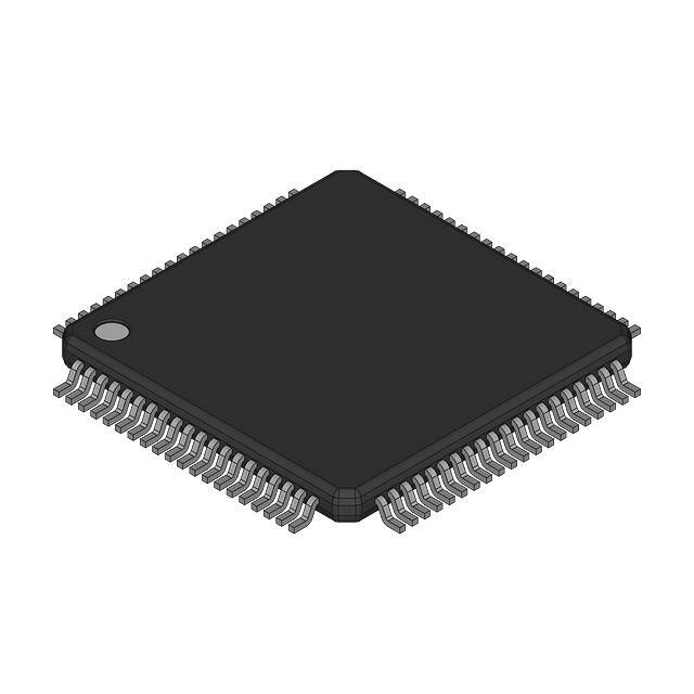


 工商网监
湘ICP备2023018690号
工商网监
湘ICP备2023018690号
