EL2140, EL2141
®
Data Sheet
October 1995, Rev. A
150MHz Differential Twisted Pair Driver
Features
The EL2140/2141 is a very high bandwidth amplifier whose output is in
differential form, and is thus primarily
targeted for applications such as driving twisted pair lines, or any application where common
mode injection is likely to occur. The input signal can be in
either single-ended or differential form, but the output is
always in differential form.
• Fully differential inputs, outputs, and feedback
On the EL2141, two feedback inputs provide the user with
the ability to set the device gain, (stable at minimum gain of
two), whereas the EL2140 comes with a fixed gain of two.
The output common mode level is set by the reference pin
(VREF), which has a -3dB bandwidth of over 100MHz. Generally, this pin is grounded, but it can be tied to any voltage
reference.
• Differential input range ±2.3V
• 150MHz 3dB bandwidth
• 800V/Ps slew rate
• -55dB distortion at 3MHz
• -75dB distortion at 100kHz
• ±5V supplies or +6V single supply
• 50mA minimum output current
• Output swing (200: load) to within 1.5V of supplies
(14VPKPK differential)
• Low power-11mA typical supply current
The transmission of ADSL/HDSL signals requires very low
distortion amplification, so this amplifier was designed with
this as a primary goal. The actual signal distortion levels
depend upon input and output signal amplitude, as well as
the output load impedance. (See distortion data inside.)
Applications
Both outputs (VOUT, VOUTB) are short circuit protected to
withstand temporary overload condition.
• VGA over twisted pair
Ordering Information
• Single ended to differential amplification
PART
NUMBER
FN7048
• Twisted pair driver
• Differential line driver
• ADSL/HDSL driver
• Transmission of analog signals in a noisy environment
TEMP. RANGE
PACKAGE
PKG. NO.
EL2140CN
-40°C to +85°C
8-pin PDIP
MDP0031
EL2140CS
-40°C to +85°C
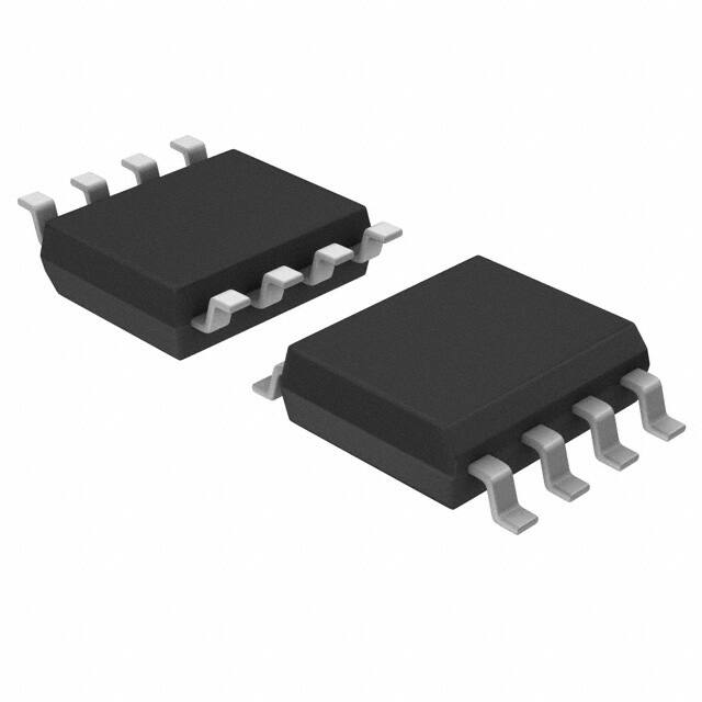
8-pin SOIC
MDP0027
EL2141CN
-40°C to +85°C
8-pin PDIP
MDP0031
EL2141CS
-40°C to +85°C
8-pin SOIC
MDP0027
Pinouts
EL2140
(8-PIN SOIC, PDIP)
TOP VIEW
1
EL2141
(8-PIN SOIC, PDIP)
TOP VIEW
CAUTION: These devices are sensitive to electrostatic discharge; follow proper IC Handling Procedures.
1-888-INTERSIL or 321-724-7143 | Intersil (and design) is a registered trademark of Intersil Americas Inc.
Copyright © Intersil Americas Inc. 2003. All Rights Reserved. Elantec is a registered trademark of Elantec Semiconductor, Inc.
All other trademarks mentioned are the property of their respective owners.
�EL2140, EL2141
Absolute Maximum Ratings (TA = 25°C)
Supply Voltage VS+ and GND . . . . . . . . . . . . . . . . . . . . . . . . +12.6V
Maximum Output Current. . . . . . . . . . . . . . . . . . . . . . . . . . . . ±60mA
Storage Temperature Range . . . . . . . . . . . . . . . . . .-65°C to +150°C
Operating Junction Temperature . . . . . . . . . . . . . . . . . . . . . . +150°C
Recommended Operating Temperature . . . . . . . . . . . -40°C to 85°C
VIN, VINB, VREF. . . . . . . . . . . . VEE+0.8V (MIN) to VCC-0.8V (MAX)
VIN–VINB . . . . . . . . . . . . . . . . . . . . . . . . . . . . . . . . . . . . . . . . . . .±5V
CAUTION: Stresses above those listed in “Absolute Maximum Ratings” may cause permanent damage to the device. This is a stress only rating and operation of the
device at these or any other conditions above those indicated in the operational sections of this specification is not implied.
IMPORTANT NOTE: All parameters having Min/Max specifications are guaranteed. Typical values are for information purposes only. Unless otherwise noted, all tests
are at the specified temperature and are pulsed tests, therefore: TJ = TC = TA
DC Electrical Specifications
VCC = +5V, VEE = -5V, TA = 25°C, VIN = 0V, RL = 200, unless otherwise specified.
PARAMETER
DESCRIPTION
MIN
TYP
MAX
UNITS
±3.0
±5.0
±6.3
V
11
14
mA
VSUPPLY
Supply Operating Range (VCC–VEE)
IS
Power Supply Current (No Load)
VOS
Input Referred Offset Voltage
-25
10
40
mV
IIN
Input Bias Current (VIN, VINB, VREF)
-20
6
20
PA
ZIN
Differential Input Impedance
VDIFF
Differential Input Range
AV
Voltage Gain (EL2140) VIN = 2VPK-PK
AVOL
Open Loop Voltage Gain (EL2141)
VCM
Input Common Mode Voltage Range (EL2140)
-2.6
VOUT(200)
Output Voltage Swing (200: load, VOUT to VOUTB) (EL2141)
±3.4
±3.6
V
VOUT(100)
Output Voltage Swing (100: Load, VOUT to VOUTB) (EL2141)
±2.9
±3.1
V
VN
Input Referred Voltage Noise
36
nV/Hz
VREF
Output Voltage Control Range (EL2140)
-2.5
VREFOS
Output Offset Relative to VREF
-60
-25
PSRR
Power Supply Rejection Ratio
60
70
dB
IOUT(min)
Minimum Output Current
50
60
mA
CMRR
Input Common Mode Rejection Ratio (EL2140) VCM = ±2V
60
70
dB
ROUT
(VOUT = VOUTB = 0V) Output Impedance
0.1
:
2
400
k:
±2.0
±2.3
V
1.95
1.985
2.02
75
V/V
dB
+4.0
V
+3.3
V
+60
mV
�EL2140, EL2141
AC Electrical Specifications
VCC = +5V, VEE = -5V, TA = 25°C, VIN = 0V, RLOAD = 200, unless otherwise specified
PARAMETER
DESCRIPTION
MIN
TYP
MAX
UNITS
BW(-3dB)
-3dB Bandwidth (EL2140 and EL2141 @ gain of 2)
150
MHz
SR
Differential Slewrate
800
V/Ps
Tstl
Settling Time to 1%
15
ns
GBW
Gain Bandwidth Product
400
MHz
VREFBW(-3dB)
VREF -3dB Bandwidth
130
MHz
VREFSR
VREF Slewrate
100
V/Ps
THDf1
Distortion at 100kHz (Note 1)
-75
dB
dP
Differential Phase @ 3.58MHz
0.16
°
dG
Differential Gain @ 3.58MHz
0.24
%
NOTE:
1. Distortion measurement quoted for VOUT–VOUTB = 12V pk-pk, RLOAD = 200:, VGAIN = 8
Pin Descriptions
PIN NO.
EL2140
EL2141
PIN NAME
1
2
VIN
3
FUNCTION
Non-inverting Input
VINB
Inverting Input (EL2140 only)
1
FBP
Non-inverting Feedback Input. Resistor R1 must be Connected from this Pin to VOUT. (EL2141 only)
4
FBN
Inverting Feedback Input. Resistor R3 must be Connected from this pin to VOUTB. (EL2141 only)
4
3
VREF
Output Common-mode Control. The Common-mode Voltage of VOUT and VOUTB will Follow the Voltage
on this Pin. Note that on the EL2141, this pin is also the VINB pin.
5
5
VOUTB
Inverting Output
6
6
VCC
Positive Supply
7
7
VEE
Negative Supply
8
8
VOUT
3
Non-inverting Output
�EL2140, EL2141
Typical Performance Curves
IS vs Supply Voltage
EL2141 Frequency Response
vs Resistor R2 (Gain = 2)
EL2141 Frequency Response
vs Resistor R2 (Gain = 8)
4
EL2140 Frequency Response
Frequency Response vs
Temperature
EL2141 Distortion vs Frequency
(Gain = 6, RLOAD = 200:)
VIN = 2VPK-PK
�EL2140, EL2141
Typical Performance Curves
(Continued)
EL2140 CMRR vs Frequency
EL2141 Output Signal and Common
Mode Signal vs Frequency
EL2140 VREF Frequency Response
EL2140 Small Signal Response (NOTE)
NOTE: Photo Shows Voltages On A 100: Transmission Line Terminated At Both Ends, So Voltages At VOUT, VOUTB
Are Twice The Values Shown.
5
�EL2140, EL2141
Applications Information
EL2141
EL2140
Gain = 2
V OUT + V OUT B
------------------------------------------ = V REF
2
R1 + R2 + R3
GAIN = ------------------------------------R2
Choice of Feedback Resistor
There is little to be gained from choosing resistor R2 values
below 400:�and, in fact, it would only result in increased
power dissipation and signal distortion. Above 400:, the
bandwidth response will develop some peaking (for a gain of
two), but substantially higher resistor R2 values may be used
for higher voltage gains, such as up to 2k: at a gain of eight
before peaking will develop. R1 and R3 are selected as
needed to set the voltage gain, and while R1 = R3 is suggested, the gain equation above holds for any values (see
distortion for further suggestions).
Capacitance Considerations
As with many high bandwidth amplifiers, the EL2140/2141
prefer not to drive highly capacitive loads. It is best if the
capacitance on VOUT and VOUTB is kept below 10pF if the
user does not want gain peaking to develop.
In addition, on the EL2141, the two feedback nodes FBP and
FBN should be laid out so as to minimize stray capacitance,
else an additional pole will potentially develop in the
response with possible gain peaking.
The amount of capacitance tolerated on any of these nodes
in an actual application will also be dependent on the gain
setting and the resistor values in the feedback network.
Distortion Considerations
The harmonics that these amplifiers will potentially produce
are the 2nd, 3rd, 5th, and 6th. Their amplitude is application
dependent. All other harmonics should be negligible by comparison. Each should be considered separately:
H2 The second harmonic arises from the input stage, and
the lower the applied differential signal amplitude, the lower
the magnitude of the second harmonic. For practical considerations of required output signal and input noise levels, the
user will end up choosing a circuit gain. Referring to Figure 1,
it is best if the voltage at the negative feedback node tracks
the VREF node, and the voltage at the positive feedback
node tracks the VIN node respectively. This would theoretically require that R1 + R2 = R3, although the lowest
distortion is found at about R3 = R1 + (0.7*R2). With this
6
(COMMON MODE)
arrangement, the second harmonic should be suppressed
well below the value of the third harmonic.
H3 The third harmonic should be the dominant harmonic and
is primarily affected by output load current which, of course,
is unavoidable. However, this should encourage the user not
to waste current in the gain setting resistors, and to use values that consume only a small proportion of the load current,
so long as peaking does not occur. The more load current,
the worse the distortion, but depending on the frequency, it
may be possible to reduce the amplifier gain so that there is
more internal gain left to cancel out any distortion.
H5 The fifth harmonic should always be below the third, and
will not become significant until heavy load currents are
drawn. Generally, it should respond to the same efforts
applied to reducing the third harmonic.
H6 The sixth harmonic should not be a problem and is the
result of poor power supply decoupling. While 100nF chip
capacitors may be sufficient for some applications, it would
be insufficient for driving full signal swings into a twisted pair
line at 100kHz. Under these conditions, the addition of 4.7PF
tantalum capacitors would cure the problem.
�EL2140, EL2141
Typical Applications Circuits
FIGURE 1. TYPICAL TWISTED PAIR APPLICATION
FIGURE 2. DUAL COAXIAL CABLE DRIVER
FIGURE 3. SINGLE SUPPLY TWISTED PAIR DRIVER
7
�EL2140, EL2141
Typical Applications Circuits (Continued)
FIGURE 4. DIFFERENTIAL LINE DRIVER WITH EQUALIZATION
R1 + R2 + R3
DCGain = ------------------------------------- � SeeFigure5 �
R2
R1 + � R2 e R4 � + R3
� HF �Gain = ------------------------------------------------------ � SeeFigure5 �
� R2 e R4 �
1
whereF O = ---------------------2SC 1 R 2
1
andF P = ---------------------2SC 1 R 4
FIGURE 5. DUAL SIGNAL TRANSMISSION CIRCUIT
All Intersil U.S. products are manufactured, assembled and tested utilizing ISO9000 quality systems.
Intersil Corporation’s quality certifications can be viewed at www.intersil.com/design/quality
Intersil products are sold by description only. Intersil Corporation reserves the right to make changes in circuit design, software and/or specifications at any time without
notice. Accordingly, the reader is cautioned to verify that data sheets are current before placing orders. Information furnished by Intersil is believed to be accurate and
reliable. However, no responsibility is assumed by Intersil or its subsidiaries for its use; nor for any infringements of patents or other rights of third parties which may result
from its use. No license is granted by implication or otherwise under any patent or patent rights of Intersil or its subsidiaries.
For information regarding Intersil Corporation and its products, see www.intersil.com
8
�