EL2228
®
Data Sheet
May 3, 2007
Dual Low Noise Amplifier
Features
The EL2228 is a dual, low-noise amplifier, ideally suited to
filtering applications in ADSL and HDSLII designs. It features
low noise specification of just 4.9nV/√Hz and 1.2pA/√Hz,
making it ideal for processing low voltage waveforms.
• Voltage noise of only 4.9nV/√Hz
The EL2228 has a -3dB bandwidth of 80MHz and is gainof-1 stable. It also affords minimal power dissipation with a
supply current of just 4.5mA per amplifier. The amplifier can
be powered from supplies ranging from ±2.5V to ±12V.
• Gain-of-1 stable
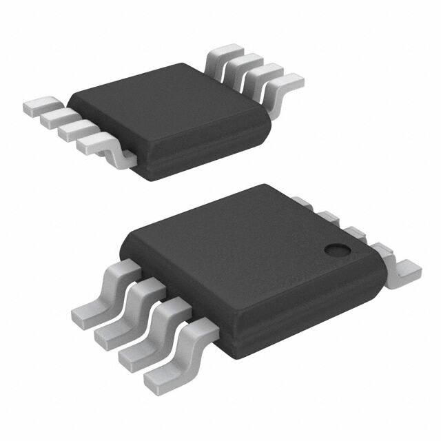
The EL2228 is available in a space saving 8 Ld MSOP
package as well as the industry-standard 8 Ld SOIC. It is
specified for operation over the -40°C to +85°C temperature
range.
FN7008.2
• Current noise of only 1.2pA/√Hz
• Bandwidth (-3dB) of 80MHz -@ AV = +1
• Just 4.5mA per amplifier
• 8 Ld MSOP package
• ±2.5V to ±12V operation
• Pb-free plus anneal available (RoHS compliant)
Applications
• ADSL filters
Pinout
• HDSLII filters
EL2228
(8 LD SOIC, 8 LD MSOP)
TOP VIEW
• Ultrasound input amplifiers
• Wideband instrumentation
8 VS+
VOUTA 1
VINA- 2
-
• Communications equipment
• Wideband sensors
7 VOUTB
+
VINA+ 3
-
6 VINB-
+
VS- 4
5 VINB+
Ordering Information
PART
NUMBER
PART
MARKING
TEMP RANGE (°C)
TAPE & REEL
PACKAGE
PKG. DWG. #
EL2228CY
N
-40 to +85
-
8 Ld MSOP (3.0mm)
MDP0043
EL2228CY-T13
N
-40 to +85
13”
8 Ld MSOP (3.0mm)
MDP0043
EL2228CY-T7
N
-40 to +85
7”
8 Ld MSOP (3.0mm)
MDP0043
EL2228CYZ (Note)
BAAAV
-40 to +85
-
8 Ld MSOP (3.0mm) (Pb-free)
MDP0043
EL2228CYZ-T13 (Note)
BAAAV
-40 to +85
13”
8 Ld MSOP (3.0mm) (Pb-free)
MDP0043
EL2228CYZ-T7 (Note)
BAAAV
-40 to +85
7”
8 Ld MSOP (3.0mm) (Pb-free)
MDP0043
EL2228CS
2228CS
-40 to +85
-
8 Ld SOIC (150 mil)
MDP0027
EL2228CS-T13
2228CS
-40 to +85
13”
8 Ld SOIC (150 mil)
MDP0027
EL2228CS-T7
2228CS
-40 to +85
7”
8 Ld SOIC (150 mil)
MDP0027
EL2228CSZ (Note)
2228CSZ
-40 to +85
-
8 Ld SOIC (150 mil) (Pb-free)
MDP0027
EL2228CSZ-T13 (Note)
2228CSZ
-40 to +85
13”
8 Ld SOIC (150 mil) (Pb-free)
MDP0027
EL2228CSZ-T7 (Note)
2228CSZ
-40 to +85
7”
8 Ld SOIC (150 mil) (Pb-free)
MDP0027
NOTE: Intersil Pb-free plus anneal products employ special Pb-free material sets; molding compounds/die attach materials and 100% matte tin plate
termination finish, which are RoHS compliant and compatible with both SnPb and Pb-free soldering operations. Intersil Pb-free products are MSL
classified at Pb-free peak reflow temperatures that meet or exceed the Pb-free requirements of IPC/JEDEC J STD-020.
1
CAUTION: These devices are sensitive to electrostatic discharge; follow proper IC Handling Procedures.
1-888-INTERSIL or 1-888-468-3774 | Intersil (and design) is a registered trademark of Intersil Americas Inc.
Copyright Intersil Americas Inc. 2002, 2003, 2005, 2007. All Rights Reserved
All other trademarks mentioned are the property of their respective owners.
�EL2228
Absolute Maximum Ratings (TA = +25°C)
Thermal Information
Supply Voltage between VS+ and VS- . . . . . . . . . . . . . . . . . . . .+28V
Input Voltage . . . . . . . . . . . . . . . . . . . . . . . . . . VS- - 0.3V, VS +0.3V
Maximum Continuous Output Current . . . . . . . . . . . . . . . . . . . 40mA
ESD Voltage. . . . . . . . . . . . . . . . . . . . . . . . . . . . . . . . . . . . . . . . .2kV
Maximum Die Temperature . . . . . . . . . . . . . . . . . . . . . . . . . . +150°C
Storage Temperature . . . . . . . . . . . . . . . . . . . . . . . .-65°C to +150°C
Power Dissipation . . . . . . . . . . . . . . . . . . . . . . . . . . . . . See Curves
Operating Temperature . . . . . . . . . . . . . . . . . . . . . . .-40°C to +85°C
Pb-free reflow profile . . . . . . . . . . . . . . . . . . . . . . . . . .see link below
http://www.intersil.com/pbfree/Pb-FreeReflow.asp
CAUTION: Stresses above those listed in “Absolute Maximum Ratings” may cause permanent damage to the device. This is a stress only rating and operation of the
device at these or any other conditions above those indicated in the operational sections of this specification is not implied.
NOTE: All parameters having Min/Max specifications are guaranteed. Typ values are for information purposes only. Unless otherwise noted, all tests are at the specified
temperature and are pulsed tests, therefore: TJ = TC = TA
Electrical Specifications
PARAMETER
VS+ = +12V, VS- = -12V, RL = 500Ω and CL = 3pF to 0V, RF = 420Ω and TA = +25°C Unless Otherwise
Specified.
DESCRIPTION
CONDITIONS
MIN
TYP
MAX
UNIT
3
mV
INPUT CHARACTERISTICS
VOS
Input Offset Voltage
VCM = 0V
0.2
TCVOS
Average Offset Voltage Drift
Measured over operating temperature range
-4
IB
Input Bias Current
VCM = 0V
RIN
Input Impedance
8
MΩ
CIN
Input Capacitance
1
pF
CMIR
Common-Mode Input Range
CMRR
Common-Mode Rejection Ratio
-9
-4.5
-11.8
µV/°C
-1
+10.4
µA
V
for VIN from -11.8V to +10.4V
60
90
dB
for VIN from -10V to +10V
60
75
dB
60
75
dB
AVOL
Open-Loop Gain
-5V ≤ VOUT ≤ 5V
eN
Voltage Noise
f = 100kHz
4.9
nV/√Hz
iN
Current Noise
f = 100kHz
1.2
pA/√Hz
RL = 500Ω
-10.3
-10
V
RL = 250Ω
-9.5
-9
V
OUTPUT CHARACTERISTICS
VOL
VOH
ISC
Output Swing Low
Output Swing High
Short Circuit Current
RL = 500Ω
10
10.3
V
RL = 250Ω
9.5
10
V
RL = 10Ω
140
180
mA
dB
POWER SUPPLY PERFORMANCE
PSRR
Power Supply Rejection Ratio
VS is moved from ±10.8V to ±13.2V
65
83
IS
Supply Current (per Amplifier)
No load
4
5
44
65
V/µs
50
ns
80
MHz
f = 1MHz, VO = 2VP-P, RL = 500Ω, AV = 2
-86
dBc
f = 1MHz, VO = 2VP-P, RL = 150Ω, AV = 2
-79
dBc
f = 1MHz, VO = 2VP-P, RL = 500Ω, AV = 2
-93
dBc
f = 1MHz, VO = 2VP-P, RL = 150Ω, AV = 2
-70
dBc
6
mA
DYNAMIC PERFORMANCE
SR
Slew Rate (Note 1)
±2.5V square wave, measured 25% to 75%
tS
Settling to +0.1% (AV = +1)
(AV = +1), VO = 2V step
BW
-3dB Bandwidth
HD2
2nd Harmonic Distortion
HD3
3rd Harmonic Distortion
NOTE:
1. Slew rate is measured on rising and falling edges
2
FN7008.2
May 3, 2007
�EL2228
Electrical Specifications
PARAMETER
VS+ = +5V, VS- = -5V, RL = 500Ω and CL = 3pF to 0V, RF = 420Ω and TA = +25°C unless otherwise specified.
DESCRIPTION
CONDITIONS
MIN
TYP
MAX
UNIT
3
mV
INPUT CHARACTERISTICS
VOS
Input Offset Voltage
VCM = 0V
0.6
TCVOS
Average Offset Voltage Drift
Measured over operating temperature range
4.9
IB
Input Bias Current
VCM = 0V
RIN
Input Impedance
6
MΩ
CIN
Input Capacitance
1.2
pF
CMIR
Common-Mode Input Range
CMRR
Common-Mode Rejection Ratio
-9
-4.5
-4.7
for VIN from -4.7V to +3.4V
60
µV/°C
-1
+3.4
90
Open-Loop Gain
-2.5V ≤ VOUT ≤ 2.5V
eN
Voltage Noise
iN
Current Noise
V
dB
for VIN from -2V to +2V
AVOL
µA
dB
60
72
dB
f = 100kHz
4.7
nV/√Hz
f = 100kHz
1.2
pA/√Hz
RL = 500Ω
-3.8
-3.5
V
RL = 250Ω
-3.7
-3.5
V
OUTPUT CHARACTERISTICS
VOL
VOH
ISC
Output Swing Low
Output Swing High
Short Circuit Current
RL = 500Ω
3.5
3.7
V
RL = 250Ω
3.5
3.6
V
RL = 10Ω
60
100
mA
dB
POWER SUPPLY PERFORMANCE
PSRR
Power Supply Rejection Ratio
VS is moved from ±4.5V to ±5.5V
65
83
IS
Supply Current (Per Amplifier)
No load
3.5
4.5
35
50
V/µs
50
ns
75
MHz
f = 1MHz, VO = 2VP-P, RL = 500Ω, AV = 2
-90
dBc
f = 1MHz, VO = 2VP-P, RL = 150Ω, AV = 2
-71
dBc
f = 1MHz, VO = 2VP-P, RL = 500Ω, AV = 2
-99
dBc
f = 1MHz, VO = 2VP-P, RL = 150Ω, AV = 2
-69
dBc
5.5
mA
DYNAMIC PERFORMANCE
SR
Slew Rate (Note 1)
±2.5V square wave, measured 25%-75%
tS
Settling to +0.1% (AV = +1)
(AV = +1), VO = 2V step
BW
-3dB Bandwidth
HD2
2nd Harmonic Distortion
HD3
3rd Harmonic Distortion
NOTE:
1. Slew rate is measured on rising and falling edges
3
FN7008.2
May 3, 2007
�EL2228
Typical Performance Curves
Non-Inverting Frequency Response for Various RF
Inverting Frequency Response for Various RF
4
4
3
2
RF = 1kΩ
1
RF = 420Ω
0
-1
RF=200Ω
-2
RF=0Ω
-3
-4
-5
VS = ±12V
AV = +1
RL = 500Ω
-6
100k
Normalized Gain (dB)
Normalized Gain (dB)
3
2
RF = 100Ω
1
-1
RF = 1kΩ
-2
-3
-4
-5
1M
-6
1M
100M
10M
VS = ±12V
AV = -1
RL = 500Ω
Frequency (Hz)
Non-Inverting Frequency Response (Gain)
2
Inverting Frequency Response (Gain)
4
VS=±12V
RF=420Ω
RL=500Ω
3
AV = 1
1
0
AV = 2
-1
AV = 10
-2
AV = 5
-3
-4
Normalized Gain (dB)
Normalized Gain (dB)
3
-5
2
VS = ±12V
RF = 420Ω
1
AV = -1
0
-1
AV = -10
AV = -2
-2
AV = -5
-3
-4
-5
-6
100k
1M
-6
100k
100M
10M
1M
Frequency (Hz)
Inverting Frequency Response (Phase)
Non-Inverting Frequency Response (Phase)
135
90
90
45
-45
AAVV=
=55
-90
-135
AVA=10
V = 10
-180
-270
10M
AV = -5
-90
-135
-225
1M
AV = -2
-45
AV = -10
-180
V
VSS=±12
= ±12V
V
RF = 420Ω
R
RFL=420
= 500Ω
-315
100k
AV = -1
0
AAVV=
=22
Phase (°)
Phase (°)
45
AAVV=
=11
0
-270
VS = ±12V
RF = 420Ω
RL = 500Ω
-315
100k
100M
1M
2
1
Non-Inverting Frequency Response for Various
Input Signal Levels
VS = ±12V
RF = 420Ω
RL = 500Ω
AV = +1
VIN = 100mVPP
-1
VIN = 1VPP
-2
VIN = 2VPP
-3
-4
-6
100k
4
3
0
-5
100M
Non-Inverting Frequency Response for Various RL
VIN = 500mVPP
1M
10M
Frequency (Hz)
4
Normalized Gain (dB)
Normalized Gain (dB)
3
10M
Frequency (Hz)
Frequency (Hz)
4
100M
10M
Frequency (Hz)
135
-225
100M
10M
Frequency (Hz)
4
RF = 420Ω
0
2
1
-1
RL = 50Ω
-2
RL = 150Ω
-3
-4
-5
100M
RL = 1kΩ
0
VS = ±12V
AV = +1
RF = 420Ω
-6
100k
RL = 500Ω
1M
10M
100M
Frequency (Hz)
FN7008.2
May 3, 2007
�EL2228
Typical Performance Curves
(Continued)
Non-Inverting Frequency Response for Various CL
4
4
3
CL = 30pF
2
Normalized Gain (dB)
Normalized Gain (dB)
3
Non-Inverting Frequency Response for Various
Output DC Levels
1
0
-1
CL = 3pF
-2
-3
CL = 10pF
VS = ±12V
RF = 420Ω
RL = 500Ω
AV = +1
-4
-5
-6
100k
2
VO = 0
-1
-2
-3
-4
VS = ±12V
RF = 420Ω
RL = 500Ω
AV = +1
-6
100k
100M
10M
60
40
G=2
0
2.5
G = 10
4.5
6.5
8.5
10.5
-3dB Bandwidth vs ± Supply Voltage for Inverting
Gains
VS = ±12V
RF = 420Ω
RL = 500Ω
AV = +1
20
15
G = -5
G = -10
5
0
2.5
12.5
4.5
Peaking (dB)
Peaking (dB)
VS = ±12V
RF = 420Ω
RL = 500Ω
AV = +1
0.16
0.4
G = -1
0.12
0.08
G = -2
0.04
G=2
0
2.5
12.5
Peaking vs ± Supply Voltage for Inverting Gains
0.6
0.2
10.5
8.5
0.2
VS = ±12V
RF = 420Ω
RL = 500Ω
AV = +1
G=1
6.5
Supply Voltage (±V)
Peaking vs ± Supply Voltage for Non-inverting
Gains
0.8
G = -2
10
Supply Voltage (±V)
1
100M
10M
G = -1
-3dB Bandwidth (MHz)
G=1
-3dB Bandwidth (MHz)
25
VS = ±12V
RF = 420Ω
RL = 500Ω
AV = +1
G=5
VO = -5
Frequency (Hz)
-3dB Bandwidth vs ± Supply Voltage for Noninverting Gains
20
VO =V+5
O=
1M
Frequency (Hz)
80
VO = +10
0
-5
1M
VO = -10
1
G = -10
G = 10
4.5
6.5
8.5
10.5
12.5
0
2.5
Supply Voltage (±V)
4.5
6.5
8.5
12.5
Small Signal Step Response
VS = ±2.5V
Small Signal Step Response
VS = ±12V
RF = 420Ω
AV = 1
RL= 500Ω
20mV/div
10.5
Supply Voltage (±V)
RF = 420Ω
AV = 1
RL= 500Ω
20mV/div
50ns/div
5
50ns/div
FN7008.2
May 3, 2007
�EL2228
Typical Performance Curves
(Continued)
Large Signal Step Response
VS = ±12V
Large Signal Step Response
VS = ±2.5V
RF = 420Ω
AV = 1
RL= 500Ω
RF = 420Ω
AV = 1
RL= 500Ω
0.5V/div
0.5V/div
50ns/div
50ns/div
Group Delay vs Frequency
20
0.2
16
VS = ±12V
RF = 420Ω
RL = 150Ω
AV = 2
0.15
12
AV = 2
8
4
dG (%) or dP (°)
Group Delay (ns)
Differential Gain/Phase vs DC Input Voltage at
3.58MHz
AV = 1
0
-4
-8
VS = ±12V
RF = 420Ω
AV = 1
RL = 500Ω
-12
-16
0.1
dP
dG
0.05
0
-0.05
-0.1
-20
1M
10M
-0.15
-1
100M 200M
-0.5
0
0.5
1
DC Input Voltage (V)
Frequency (Hz)
Supply Current vs Supply Voltage
Closed Loop Output Impedance vs Frequency
13.2
100
12
Output Impedance (Ω)
Supply Current (mA)
10.8
9.6
8.4
7.2
6
4.8
3.6
2.4
10
1
0.1
1.2
0
0
1.4
2.8
4.2
5.6
7
8.4
0.01
10k
9.8 11.2 12.6 14
100k
VS (±V)
10M
100M
PSRR vs Frequency
100
10
80
-10
60
-30
PSRR (dB)
CMRR (dB)
CMRR vs Frequency
40
20
0
10
1M
Frequency (Hz)
VS-50
VS+
-70
VS = ±12
100
1k
10k
100k
Frequency (Hz)
6
1M
10M
100M
-90
1k
10k
100k
1M
10M
100M
Frequency (Hz)
FN7008.2
May 3, 2007
�EL2228
Typical Performance Curves
-40
1MHz 2nd and 3rd Harmonic Distortion vs Output
Swing (VS = ±12V)
-50
-60
2ndHD
-60
3rdHD
-70
-80
-90
-100
1MHz 2nd and 3rd Harmonic Distortion vs Output
Swing (VS = ±2.5V)
-50
Distortion (dB)
Distortion (dB)
(Continued)
-70
3rdHD
-80
-90
2ndHD
-100
0
4
12
8
16
-110
20
0
0.5
1
Output Swing (VPP)
-50
1MHz 2nd and 3rd Harmonic Distortion vs Output
Swing (Single-Ended)
-50
-70
3rdHD
2ndHD
-90
-100
VS = ±12V
AV = 2
RF = 420Ω
-110
-120
0
4
8
12
16
2ndHD
-70
-80
3rdHD
-90
-100
-110
20
0
0.5
1
1.5
2
2.5
Output Swing (VPP)
Voltage and Current Noise vs Frequency
Channel to Channel Isolation vs Frequency
18
0
16
-20
14
12
Isolation (dB)
Voltage Noise (nV√Hz), Current Noise
2.5
VS = ±2.5V
AV = 2
RF = 420Ω
Output Swing (VPP)
10
8
EN
6
4
0
10
-40
B→C
-60
-80
IN
2
A→B
100
1k
10k
-100
100k
100k
1M
Frequency (Hz)
11
100M
10M
Frequency (Hz)
Supply Current vs Temperature
VS = ±12V
100
3dB Bandwidth vs Temperature
VS = ±5V
90
Bandwidth (MHz)
Supply Current (mA)
2
1MHz 2nd and 3rd Harmonic Distortion vs Output
Swing (Single-Ended)
-60
Distortion (dBc)
Distortion (dBc)
-60
-80
1.5
Output Swing (VPP)
10
9
80
70
60
0
-50
0
50
100
Junction Temperature (mA)
7
150
50
-40
10
60
110
160
Junction Temperature (°C)
FN7008.2
May 3, 2007
�EL2228
Typical Performance Curves
(Continued)
Input Bias Current vs Temperature
Input Offset Voltage vs Temperature
2
Input Offset Voltage (mV)
Input Bias Current (µA)
-2
-4
-6
-8
-50
0
50
100
1
0
-1
-2
-50
150
0
Junction Temperature (°C)
100
150
Package Power Dissipation vs Ambient Temperature
JEDEC JESD51-3 Low Effective Thermal Conductivity
Test Board
76
0.7
74
0.6 625mW
Power Dissipation (W)
Slew Rate (V/µs)
Slew Rate vs Temperature
72
70
68
66
0.5
SO8
160°C/W
486mW
0.4
0.3
MSOP8
206°C/W
0.2
0.1
64
62
-50
0
50
100
150
0
0
25
50
75 85 100
125
150
Ambient Temperature (°C)
Temperature (°C)
1.4
50
Junction Temperature (°C)
Package Power Dissipation vs Ambient Temperature
JEDEC JESD51-7 High Effective Thermal Conductivity
Test Board
Power Dissipation (W)
1.2
1 909mW
SO8
110°C/W
0.8 870mW
0.6
MSOP8
115°C/W
0.4
0.2
0
0
25
50
75
100
125
150
Ambient Temperature (°C)
8
FN7008.2
May 3, 2007
�EL2228
Pin Descriptions
8 Ld MSOP
8 Ld SOIC
PIN NAME
PIN
FUNCTION
1
1
VOUTA
Output
EQUIVALENT CIRCUIT
VS+
VOUT
Circuit 1
2
2
VINA-
Input
VS+
VIN+
VIN-
VS-
Circuit 2
3
3
VINA+
Input
4
4
VS-
Supply
5
5
VINB+
Input
6
6
VINB-
Input
Reference Circuit 2
7
7
VOUTB
Output
Reference Circuit 1
8
8
VS+
Supply
Applications Information
Product Description
The EL2228 is a dual voltage feedback operational amplifier
designed especially for DMT ADSL and other applications
requiring very low voltage and current noise. It also features
low distortion while drawing moderately low supply current
and is built on Elantec's proprietary high-speed
complementary bipolar process. The EL2228 uses a
classical voltage-feedback topology which allows them to be
used in a variety of applications where current-feedback
amplifiers are not appropriate because of restrictions placed
upon the feedback element used with the amplifier. The
conventional topology of the EL2228 allows, for example, a
capacitor to be placed in the feedback path, making it an
excellent choice for applications such as active filters,
sample-and-holds, or integrators.
Single-Supply Operation
The EL2228 was designed to have a wide input and output
voltage range. This design also makes the EL2228 an
9
Reference Circuit 2
excellent choice for single-supply operation. Using a single
positive supply, the lower input voltage range is within
300mV of ground (RL = 500Ω), and the lower output voltage
range is within 875mV of ground. Upper input voltage range
reaches 3.6V, and output voltage range reaches 3.8V with a
5V supply and RL = 500Ω. This results in a 2.625V output
swing on a single 5V supply. This wide output voltage range
also allows single-supply operation with a supply voltage as
high as 28V.
Gain-Bandwidth Product and the -3dB Bandwidth
The EL2228 has a gain-bandwidth product of 40MHz while
using only 5mA of supply current per amplifier. For gains
greater than 1, their closed-loop -3dB bandwidth is
approximately equal to the gain-bandwidth product divided
by the noise gain of the circuit. For gains of 1, higher-order
poles in the amplifiers' transfer function contribute to even
higher closed loop bandwidths. For example, the EL2228
have a -3dB bandwidth of 80MHz at a gain of 1, dropping to
9MHz at a gain of 5. It is important to note that the EL2228 is
designed so that this “extra” bandwidth in low-gain
FN7008.2
May 3, 2007
�EL2228
application does not come at the expense of stability. As
seen in the typical performance curves, the EL2228 in a gain
of only 1 exhibited 0.5dB of peaking with a 500Ω load.
where:
• TMAX = Maximum ambient temperature
• θJA = Thermal resistance of the package
Output Drive Capability
The EL2228 is designed to drive a low impedance load. It
can easily drive 6VP-P signal into a 500Ω load. This high
output drive capability makes the EL2228 an ideal choice for
RF, IF, and video applications. Furthermore, the EL2228 is
current-limited at the output, allowing it to withstand
momentary short to ground. However, the power dissipation
with output-shorted cannot exceed the power dissipation
capability of the package.
• PDMAX = Maximum power dissipation of 1 amplifier
• VS = Supply voltage
• IMAX = Maximum supply current of 1 amplifier
• VOUTMAX = Maximum output voltage swing of the
application
• RL = Load resistance
Driving Cables and Capacitive Loads
Power Supply Bypassing And Printed Circuit
Board Layout
Although the EL2228 is designed to drive low impedance
load, capacitive loads will decreases the amplifier's phase
margin. As shown in the performance curves, capacitive
load can result in peaking, overshoot and possible
oscillation. For optimum AC performance, capacitive loads
should be reduced as much as possible or isolated with a
series resistor between 5Ω to 20Ω. When driving coaxial
cables, double termination is always recommended for
reflection-free performance. When properly terminated, the
capacitance of the coaxial cable will not add to the capacitive
load seen by the amplifier.
As with any high frequency devices, good printed circuit
board layout is essential for optimum performance. Ground
plane construction is highly recommended. Pin lengths
should be kept as short as possible. The power supply pins
must be closely bypassed to reduce the risk of oscillation.
The combination of a 4.7µF tantalum capacitor in parallel
with 0.1µF ceramic capacitor has been proven to work well
when placed at each supply pin. For single supply operation,
where pin 4 (VS-) is connected to the ground plane, a single
4.7µF tantalum capacitor in parallel with a 0.1µF ceramic
capacitor across pin 8 (VS+).
Power Dissipation
For good AC performance, parasitic capacitance should be
kept to a minimum. Ground plane construction again should
be used. Small chip resistors are recommended to minimize
series inductance. Use of sockets should be avoided since
they add parasitic inductance and capacitance which will
result in additional peaking and overshoot.
With the wide power supply range and large output drive
capability of the EL2228, it is possible to exceed the 150°C
maximum junction temperatures under certain load and
power-supply conditions. It is therefore important to calculate
the maximum junction temperature (TJMAX) for all
applications to determine if power supply voltages, load
conditions, or package type need to be modified for the
EL2228 to remain in the safe operating area. These
parameters are related as follows:
T JMAX = T MAX + ( θ JA xPD MAXTOTAL )
where:
• PDMAXTOTAL is the sum of the maximum power
dissipation of each amplifier in the package (PDMAX)
• PDMAX for each amplifier can be calculated as follows:
V OUTMAX
PD MAX = 2*V S × I SMAX + ( V S - V OUTMAX ) × ---------------------------R
L
10
FN7008.2
May 3, 2007
�EL2228
Small Outline Package Family (SO)
A
D
h X 45°
(N/2)+1
N
A
PIN #1
I.D. MARK
E1
E
c
SEE DETAIL “X”
1
(N/2)
B
L1
0.010 M C A B
e
H
C
A2
GAUGE
PLANE
SEATING
PLANE
A1
0.004 C
0.010 M C A B
L
b
0.010
4° ±4°
DETAIL X
MDP0027
SMALL OUTLINE PACKAGE FAMILY (SO)
INCHES
SYMBOL
SO-14
SO16 (0.300”)
(SOL-16)
SO20
(SOL-20)
SO24
(SOL-24)
SO28
(SOL-28)
TOLERANCE
NOTES
A
0.068
0.068
0.068
0.104
0.104
0.104
0.104
MAX
-
A1
0.006
0.006
0.006
0.007
0.007
0.007
0.007
±0.003
-
A2
0.057
0.057
0.057
0.092
0.092
0.092
0.092
±0.002
-
b
0.017
0.017
0.017
0.017
0.017
0.017
0.017
±0.003
-
c
0.009
0.009
0.009
0.011
0.011
0.011
0.011
±0.001
-
D
0.193
0.341
0.390
0.406
0.504
0.606
0.704
±0.004
1, 3
E
0.236
0.236
0.236
0.406
0.406
0.406
0.406
±0.008
-
E1
0.154
0.154
0.154
0.295
0.295
0.295
0.295
±0.004
2, 3
e
0.050
0.050
0.050
0.050
0.050
0.050
0.050
Basic
-
L
0.025
0.025
0.025
0.030
0.030
0.030
0.030
±0.009
-
L1
0.041
0.041
0.041
0.056
0.056
0.056
0.056
Basic
-
h
0.013
0.013
0.013
0.020
0.020
0.020
0.020
Reference
-
16
20
24
28
Reference
-
N
SO-8
SO16
(0.150”)
8
14
16
Rev. M 2/07
NOTES:
1. Plastic or metal protrusions of 0.006” maximum per side are not included.
2. Plastic interlead protrusions of 0.010” maximum per side are not included.
3. Dimensions “D” and “E1” are measured at Datum Plane “H”.
4. Dimensioning and tolerancing per ASME Y14.5M-1994
11
FN7008.2
May 3, 2007
�EL2228
Mini SO Package Family (MSOP)
0.25 M C A B
D
MINI SO PACKAGE FAMILY
(N/2)+1
N
E
MDP0043
A
E1
MILLIMETERS
PIN #1
I.D.
1
B
(N/2)
e
H
C
SEATING
PLANE
0.10 C
N LEADS
SYMBOL
MSOP8
MSOP10
TOLERANCE
NOTES
A
1.10
1.10
Max.
-
A1
0.10
0.10
±0.05
-
A2
0.86
0.86
±0.09
-
b
0.33
0.23
+0.07/-0.08
-
c
0.18
0.18
±0.05
-
D
3.00
3.00
±0.10
1, 3
E
4.90
4.90
±0.15
-
E1
3.00
3.00
±0.10
2, 3
e
0.65
0.50
Basic
-
L
0.55
0.55
±0.15
-
L1
0.95
0.95
Basic
-
N
8
10
Reference
-
0.08 M C A B
b
Rev. D 2/07
NOTES:
1. Plastic or metal protrusions of 0.15mm maximum per side are not
included.
L1
2. Plastic interlead protrusions of 0.25mm maximum per side are
not included.
A
3. Dimensions “D” and “E1” are measured at Datum Plane “H”.
4. Dimensioning and tolerancing per ASME Y14.5M-1994.
c
SEE DETAIL "X"
A2
GAUGE
PLANE
L
A1
0.25
3° ±3°
DETAIL X
All Intersil U.S. products are manufactured, assembled and tested utilizing ISO9000 quality systems.
Intersil Corporation’s quality certifications can be viewed at www.intersil.com/design/quality
Intersil products are sold by description only. Intersil Corporation reserves the right to make changes in circuit design, software and/or specifications at any time without
notice. Accordingly, the reader is cautioned to verify that data sheets are current before placing orders. Information furnished by Intersil is believed to be accurate and
reliable. However, no responsibility is assumed by Intersil or its subsidiaries for its use; nor for any infringements of patents or other rights of third parties which may result
from its use. No license is granted by implication or otherwise under any patent or patent rights of Intersil or its subsidiaries.
For information regarding Intersil Corporation and its products, see www.intersil.com
12
FN7008.2
May 3, 2007
�