EL5001
6-Channel Clock Driver
DATASHEET
IGNS
EW DES
N
R
O
F
DED
EMENT
OMMEN
REPL AC
D
E
NO T REC
D
N
ter at
E
OMM
port Cen /tsc
p
u
S
l
NO REC
a
m
nic
tersil.co
our Tech
contact ERSIL or www.in
T
1-888-IN
The EL5001 is a 6-channel level shifting driver designed
primarily for use as a clock driver in LTPS LCD displays. The
EL5001 buffers and level shifts six logic level input signals.
The six channels are grouped in to two sets, one of two
channels and one of four channels. Each set can be
configured in the inverting or non-inverting modes.
Operating from 3.3V input logic, the output swing is set using
two reference input pins. These pins can be up to 18V
differential and are not buffered, so should therefore be
bypassed effectively.
Features
The EL5001 is designed to drive capacitive loads of 500pF
with rise and fall times of just 20ns. A three-state pin is
provided to set all outputs in to a high impedance mode. The
ENABLE pin can be used to put the device in to a power
save mode where the power consumption drops to just 3µA.
• Disable function
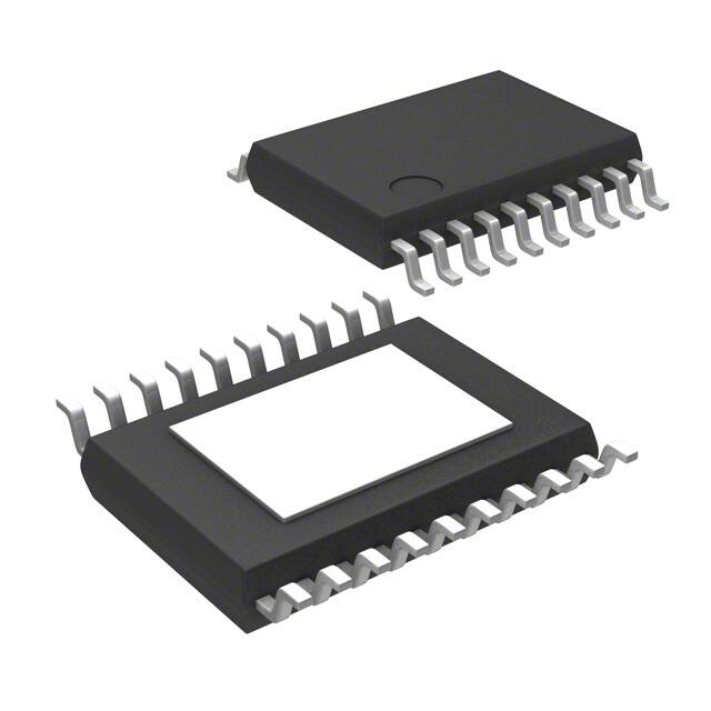
The EL5001 is available in 20-pin QFN (4mm x 4mm) and
HTSSOP packages. Both are specified for operation over
the -40°C to +85°C temperature range.
FN7376
Rev 2.00
January 31, 2005
• SIx inverting/non-inverting channels
• 3.3V input logic
• 18V output
• 250µA typical supply current
• Drives up to 500pF
• TR/TF = 35ns max
• 20-pin QFN (4mm x 4mm) and HTSSOP packages
• Pb-free available (RoHS compliant)
Applications
• LTPS LCD clock drivers
• CCD driving
• Level shifters
Ordering Information
PART NUMBER
PACKAGE
TAPE &
REEL
PKG. DWG. #
PART NUMBER
PACKAGE
TAPE &
REEL
PKG. DWG. #
EL5001IL
20-Pin QFN
(4mm x 4mm)
-
MDP0046
EL5001IRE
20-Pin
HTSSOP
-
MDP0048
EL5001IL-T7
20-Pin QFN
(4mm x 4mm)
7”
MDP0046
EL5001IRE-T7
20-Pin
HTSSOP
7”
MDP0048
EL5001IL-T13
20-Pin QFN
(4mm x 4mm)
13”
MDP0046
EL5001IRE-T13
20-Pin
HTSSOP
13”
MDP0048
EL5001ILZ
(See Note)
20-Pin QFN
(4mm x 4mm)
(Pb-Free)
-
MDP0046
EL5001IREZ
(See Note)
20-Pin
HTSSOP
(Pb-Free)
-
MDP0048
EL5001ILZ-T7
(See Note)
20-Pin QFN
(4mm x 4mm)
(Pb-Free)
7”
MDP0046
EL5001IREZ-T7
(See Note)
20-Pin
HTSSOP
(Pb-Free)
7”
MDP0048
EL5001ILZ-T13
(See Note)
20-Pin QFN
(4mm x 4mm)
(Pb-Free)
13”
MDP0046
EL5001IREZ-T13
(See Note)
20-Pin
HTSSOP
(Pb-Free)
13”
MDP0048
NOTE: Intersil Pb-free products employ special Pb-free material sets; molding compounds/die attach materials and 100% matte tin plate termination
finish, which are RoHS compliant and compatible with both SnPb and Pb-free soldering operations. Intersil Pb-free products are MSL classified at Pbfree peak reflow temperatures that meet or exceed the Pb-free requirements of IPC/JEDEC J STD-020C.
FN7376 Rev 2.00
January 31, 2005
Page 1 of 8
�EL5001
Pinouts
16 NC
17 VH
18 GND
19 TRI
20 EN
EL5001
[20-PIN QFN (4MM X 4MM)]
TOP VIEW
IN1 1
15 OUT1
IN2 2
14 OUT2
THERMAL
PAD
IN3 3
13 OUT3
FN7376 Rev 2.00
January 31, 2005
OUT6 10
VL 9
11 OUT5
INV2 8
IN5 5
INV1 7
12 OUT4
IN6 6
IN4 4
EL5001
(20-PIN HSSOP)
TOP VIEW
TRI 1
20 GND
EN 2
19 VH
IN1 3
18 OUT1
IN2 4
17 OUT2
IN3 5
IN4 6
THERMAL
PAD
16 OUT3
15 OUT4
IN5 7
14 OUT5
IN6 8
13 OUT6
INV1 9
12 VL
INV2 10
11 NC
Page 2 of 8
�EL5001
Absolute Maximum Ratings (TA = 25°C)
Supply Voltage between VSD and GND . . . . . . . . . . . . . . . . . . .18V
Maximum Continuous Output Current . . . . . . . . . . . . . . . . . . . 50mA
Ambient Operating Temperature . . . . . . . . . . . . . . . .-40°C to +85°C
Maximum Die Temperature . . . . . . . . . . . . . . . . . . . . . . . . . . +125°C
Storage Temperature . . . . . . . . . . . . . . . . . . . . . . . .-65°C to +150°C
Power Dissipation . . . . . . . . . . . . . . . . . . . . . . . . . . . . . See Curves
CAUTION: Stresses above those listed in “Absolute Maximum Ratings” may cause permanent damage to the device. This is a stress only rating and operation of the
device at these or any other conditions above those indicated in the operational sections of this specification is not implied.
IMPORTANT NOTE: All parameters having Min/Max specifications are guaranteed. Typical values are for information purposes only. Unless otherwise noted, all tests
are at the specified temperature and are pulsed tests, therefore: TJ = TC = TA
Electrical Specifications
PARAMETER
VH = 10V, VL = -5V, EN = 3V, unless otherwise specified.
DESCRIPTION
CONDITION
MIN
TYP
MAX
UNIT
EN = 3V, INX = 0V
750
1200
µA
EN = 3V, INX = 3V
250
500
µA
EN = 0V, INX = 0V
3
POWER SUPPLY
IS
Supply Current
IS_DIS
Supply Current - Disabled
VLR
VL Range
-13
0
V
VHR
VH Range
5
18
V
VH-VL
Maximum VH - VL Range
0
18
V
µA
INPUT
VIH
Logic ‘1’ Input Voltage
IIH
Logic ‘1’ Input Current
VIL
Logic ‘0’ Input Voltage
IIL
Logic ‘0’ Input Current
0.1
CIN
Input Capacitance
3.5
pF
RIN
Input Resistance
50
M
9.88
V
2.0
V
0.1
10
µA
0.8
V
10
µA
OUTPUT
VOH
VOUTL High
INX = 10V, IL = 10mA
VOL
VOUTL Low
INX = 0V, IL = -10mA
ROH
On Resistance VH to OUT
ROL
On Resistance VL to OUT
IPEAK
Peak Output Current
500
IL
Out Leakage Current
0.1
0.5
µA
9.80
-4.90
-4.88
V
IL = 50mA
11
15
IL = 50mA
11
15
mA
SWITCHING CHARACTERISTICS
tR
Rise Time
CL = 500pF
20
35
ns
tF
Fall Time
CL = 500pF
20
35
ns
tRFD
TR, TF Matching
CL = 500pF
5
ns
tD+
Turn On Delay
CL = 500pF
55
ns
tD-
Turn Off Delay
CL = 500pF
55
ns
tDD
tD+, tD-, Matching
CL = 500pF
5
ns
tEN
Enable Time
9.8
µs
tDIS
Disable Time
2.2
µs
FN7376 Rev 2.00
January 31, 2005
Page 3 of 8
�EL5001
RL=0
CL=500pF
VS=V-=0V
VS=V+=18V
RISE TIME
T=37.55ns
VOLTAGE (1V/DIV)
VOLTAGE (1V/DIV)
Typical Performance Curves
TIME (40ns/DIV)
TIME (40ns/DIV)
RISE TIME
T=23.63ns
FIGURE 2. FALL TIME OUTPUT 6VP-P
VOLTAGE (2V/DIV)
VOLTAGE (2V/DIV)
FIGURE 1. RISE TIME OUTPUT 6VP-P
RL=0
CL=500pF
VS=V-=0V
VS=V+=18V
TIME (20ns/DIV)
TIME (20ns/DIV)
FIGURE 5. RISE TIME OUTPUT 5VP-P
FN7376 Rev 2.00
January 31, 2005
FIGURE 4. FALL TIME OUTPUT 12VP-P
VOLTAGE (2V/DIV)
VOLTAGE (2V/DIV)
RISE TIME
T=40.08ns
FALL TIME
T=22.93ns
RL=0
CL=500pF
VS=V-=0V
VS=V+=18V
TIME (20ns/DIV)
FIGURE 3. RISE TIME OUTPUT 12VP-P
RL=0
CL=500pF
VS=V-=0V
VS=V+=18V
FALL TIME
T=29ns
RL=0
CL=500pF
VS=V-=0V
VS=V+=18V
RL=0
CL=500pF
VS=V-=0V
VS=V+=18V
FALL TIME
T=30.57ns
TIME (20ns/DIV)
FIGURE 6. FALL TIME OUTPUT 5VP-P
Page 4 of 8
�EL5001
Typical Performance Curves (Continued)
DISABLE
T=2.2µs
CH2
VOLTAGE (1V/DIV)
VOLTAGE (1V/DIV)
CH2
CH3
RL=0
CL=500pF
VS=V-=0V
VS=V+=18V
ENABLE
T=9.8µs
CH3
RL=0
CL=500pF
VS=V-=0V
VS=V+=18V
TIME (10µs/DIV)
TIME (10µs/DIV)
FIGURE 8. ENABLE RESPONSE
VOLTAGE (CH1-1V/DIV)(CH2-5V/DIV)
VOLTAGE (CH1-1V/DIV)(CH2-5V/DIV)
FIGURE 7. DISABLE RESPONSE
CH2
TURN-OFF
T=90ns
CH3
RL=0
CL=500pF
VS=V-=0V
VS=V+=18V
TURN-ON
T=90ns
CH2
CH3
RL=0
CL=500pF
VS=V-=0V
VS=V+=18V
TIME (100ns/DIV)
TIME (100ns/DIV)
RL=0
CL=500pF
VS=V-=0V
VS=V+=18V
CH3
1.78V
FIGURE 10. TURN-ON (TRI)
1.32V
GROUND
CH2
TIME (2µs/DIV)
FIGURE 11. ENABLE/DISABLE THRESHOLD
FN7376 Rev 2.00
January 31, 2005
VOLTAGE (2V/DIV)
VOLTAGE (CH2-5V/DIV)(CH3-1V/DIV)
FIGURE 9. TURN-OFF (TRI)
RL=0
CL=500pF
VS=V-=0V
VS=V+=18V
PROPAGATION
DELAY
T=52ns
TIME (40ns/DIV)
FIGURE 12. PROPAGATION DELAY
Page 5 of 8
�EL5001
Typical Performance Curves (Continued)
150
RL=0
100 CL=500pF
50
0
IIN (mA)
VOLTAGE (200mV/DIV)
RL=0
CL=500pF
VS=V-=0V
VS=V+=18V
MAXIMUM
SKEW=5.0ns
-50
-100
-150
-200
-250
-300
-2
-1
0
1
TIME (10ns/DIV)
TS
S
35
°
1.5
O
C
P2
/W
POWER DISSIPATION (W)
POWER DISSIPATION (W)
H
JA
=
2
0
1
0.5
0
1
0
25
50
75 85 100
125
0.7
JA
0.6
0.5
8
0.4
H
TS
S
= 1 OP
25
2
°C 0
/W
0.3
0.2
0
150
0
25
3
POWER DISSIPATION (W)
(4 Q
m F
m N
=1 x 4 20
50 m
° C m)
/W
JA
0.5
0.4
0.3
0.2
0.1
0
25
50
75 85 100
125
150
AMBIENT TEMPERATURE (°C)
FIGURE 17. PACKAGE POWER DISSIPATION vs AMBIENT
TEMPERATURE
FN7376 Rev 2.00
January 31, 2005
75 85 100
125
150
AMBIENT TEMPERATURE (°C)
JEDEC JESD51-3 AND SEMI G42-88 (SINGLE
LAYER) TEST BOARD
0.6
50
FIGURE 16. PACKAGE POWER DISSIPATION vs AMBIENT
TEMPERATURE
0.7 667mW
POWER DISSIPATION (W)
7
800mW
0.8
AMBIENT TEMPERATURE (°C)
0
6
0.1
FIGURE 15. PACKAGE POWER DISSIPATION vs AMBIENT
TEMPERATURE
0.8
5
JEDEC JESD51-3 LOW EFFECTIVE THERMAL
CONDUCTIVITY TEST BOARD
0.9
3 2.857W
4
FIGURE 14. INPUT CURRENT vs VOLTAGE
JEDEC JESD51-7 HIGH EFFECTIVE THERMAL
CONDUCTIVITY TEST BOARD - HTSSOP EXPOSED
DIEPAD SOLDERED TO PCB PER JESD51-5
2.5
3
VIN (V)
FIGURE 13. SKEW
3.5
2
JEDEC JESD51-7 HIGH EFFECTIVE THERMAL
CONDUCTIVITY TEST BOARD - QFN EXPOSED
DIEPAD SOLDERED TO PCB PER JESD51-5
2.500W
2.5
2
(4 Q
m F
m N
2
=4 x 4 0
0° mm
C
/W )
JA
1.5
1
0.5
0
0
25
50
75 85 100
125
150
AMBIENT TEMPERATURE (°C)
FIGURE 18. PACKAGE POWER DISSIPATION vs AMBIENT
TEMPERATURE
Page 6 of 8
�EL5001
EL5001 Test Board Circuit Layout
TRI
R1
FERRITE BEAD
50
EN
C2
33nF
R11
3.3
R2
OPEN
IN1
R3
1 TRI
GND 20
50
2 EN
VH 19
R4
3 IN1
OUT1 18
50
4 IN2
OUT2 17
R5
5 IN3
OUT3 16
50
6 IN4
OUT4 15
7 IN5
OUT5 14
8 IN6
OUT6 13
VS+
D1
MBRM120LT3
+ C3 L 1
4.7µF
C7
500pF
OUT1
IN2
C8
500pF
OUT2
IN3
R6
50
IN4
R7
50
IN5
9 INV1
VL 12
10 INV2
NC 11
C9
500pF
C10
500pF
C11
500pF
R8
C12
500pF
50
IN6
R9
OUT3
OUT4
OUT5
OUT6
FERRITE BEAD
50
C5
33nF
R12
3.3
INV1
R10
OPEN
+
C6 L 2
4.7µF
VSD2
MBRM120LT3
INV2
GND
Block Diagram
OE
VH
VS+
INPUT
GND
LEVEL
SHIFTER
3-STATE
CONTROL
OUTPUT
VSVL
FN7376 Rev 2.00
January 31, 2005
Page 7 of 8
�EL5001
Applications Information
Power Dissipation Calculation
The EL5001, a six channel high performance buffer, is
directed primarily as a clock driver to LPTS LCD display
applications. The six input channels are grouped into one
group of four inputs and one group of two inputs each with a
single pin (INV1 or INV2) to toggle the polarity from inverting
to non-inverting. Each channel consists of a single Nchannel low side driver and single P-channel high side
driver. These 11 devices pull the output to either the high or
low voltage on VH and VL respectively, depending on the
logic input signal.
When switching at high speeds, or driving heavy loads, the
EL5001 drive capability is limited by the rise in die
temperature brought about by internal power dissipation. For
reliable operation die temperature must be kept below
TJMAX (125°C). It is necessary to calculate the power
dissipation for a given application prior to selecting package
type.
A common 3-state pin is available that when activated will
pull all 6-channel outputs to the high impedance state.
Enable and disable pins turn shutdown both inputs and
outputs. Timing plots for 3-state, enable, and disable
functions are included in the characterization
documentation.
The EL5001 is available in either a 20-pin HTSSOP or QFN
(4mm x 4mm) packages to provide a choice for power
dissipation considerations.
Supply Voltage and Input Compatibility
Power dissipation may be calculated:
4
2
2
PD = V S I S + C INT V S f + C L V OUT f
1
where:
VS = Total power supply to the EL5001 (from VS+ to VS-)
VOUT = Swing on the output (VH - VL)
CL = Load capacitance
CINT = Internal load capacitance (80pF max)
IS = Quiescent supply current (3mA max)
f = Frequency
The EL5001 is designed to operate at a maximum potential
range from 0V to 18V. Because the EL5001 does not contain
a true analog switch, the positive supply must always be 4V
higher than the negative supply.
Having obtained the application's power dissipation, the
maximum junction temperature can be calculated:
All input pins are compatible with both 3V and 5V CMOS
signals. With the positive supply set to VS = 5V the EL5001
is compatible with TTL inputs.
where:
T JMAX = T MAX + JA PD
TJMAX = Maximum junction temperature (125°C)
Power Supply Bypassing
Due to the high switching currents generated by the EL5001
power supply bypassing is very important on both the
positive and negative supplies. A 4.7µF tantalum capacitor
can be used in parallel with a 0.1µF low-inductance ceramic
MLC capacitor. As with all bypass components, these should
be placed as close as possible to the supply pins. We also
recommend the VL and VH pins have some level of
bypassing especially when the device is driving highly
capacitive loads.
TMAX = Maximum ambient operating temperature
PD = Power dissipation calculated above
JA = Thermal resistance, junction to ambient, of the
application (package + PCB combination)
© Copyright Intersil Americas LLC 2004-2005. All Rights Reserved.
All trademarks and registered trademarks are the property of their respective owners.
For additional products, see www.intersil.com/en/products.html
Intersil products are manufactured, assembled and tested utilizing ISO9001 quality systems as noted
in the quality certifications found at www.intersil.com/en/support/qualandreliability.html
Intersil products are sold by description only. Intersil may modify the circuit design and/or specifications of products at any time without notice, provided that such
modification does not, in Intersil's sole judgment, affect the form, fit or function of the product. Accordingly, the reader is cautioned to verify that datasheets are
current before placing orders. Information furnished by Intersil is believed to be accurate and reliable. However, no responsibility is assumed by Intersil or its
subsidiaries for its use; nor for any infringements of patents or other rights of third parties which may result from its use. No license is granted by implication or
otherwise under any patent or patent rights of Intersil or its subsidiaries.
For information regarding Intersil Corporation and its products, see www.intersil.com
FN7376 Rev 2.00
January 31, 2005
Page 8 of 8
�


 工商网监
湘ICP备2023018690号
工商网监
湘ICP备2023018690号
