Dual Ultra Low Noise Wideband Amplifiers
EL5236, EL5237
Features
The EL5236 is a dual, low noise, 300MHz Gain Bandwidth
product Voltage Feedback Op Amp (VFA). The minimum operating
gain of 2 comes with a very low input noise voltage of 1.5nV/√ Hz
and 1.8pA/√Hz current noise. This makes this dual device ideal
for low noise differential active filters, dual channel photodiode
detectors, differential receivers with equalization, and any other
wideband, high dynamic range application.
• Bandwidth (-3dB) of 250MHz @ AV = +2
Each channel requires only 5.8mA on a ±6V supply. Minimal
performance change over a supply range of ±2.5V to ±6V is
provided (or single +5V ->+12V). Where system power is
paramount, the EL5237 dual with disable allows the amplifiers
to be separately powered down to less than 20µA/Ch.
• Gain Bandwidth Product: 300MHz
• Voltage Noise: 1.5nV/√Hz
• Current Noise: 1.8pA/√Hz
• IS: 5.8mA/Channel
• 100mA IOUT
• Fast Enable/Disable (EL5237 only)
• ±2.5V to ±6V Supply Range Operation
Applications
• Differential ADC Driver
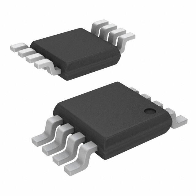
The 8 Ld dual EL5236 is available in the industry standard
pinout SO-8 or space saving MSOP-8. The 10 Ld EL5237 is
available in an MSOP-10.
• Complementary DAC Output Driver
• Ultrasound Input Amplifiers
• AGC and PLL Active Filters
• Transimpedance Designs
Related Products
• ISL28290, Dual, 80MHz, 1nV/√Hz
• ISL55290, Dual, 700MHz, 1.1nV/√Hz
422
270pF
+3.3V
39pF
+5V
255
ISL5861IB
LOW
POWER
12-BIT
DAC
130MSPS
77
25
130pF
1.27nF
0 TO 20mA
+
½ ISL5236
30pF
+5V
215
422
180pF
100
337
+
½ ISL5236
4.66k
200
77
25
1.27nF
20mA TO 0
+5V
100
255
130pF
½ ISL5236
+
180pF
215
0.1µF
422
+
-
0V CENTERED
4VP-P
DIFFERENTIAL
½ ISL5236
-5V
-5V
39pF
30pF
270pF
422
LOW POWER, LOW NOISE, DIFFERENTIAL DAC OUTPUT TRANSIMPEDANCE WITH A 5TH ORDER, 5MHz, BUTTERWORTH FILTER
FIGURE 1. TYPICAL APPLICATION
March 31, 2011
FN7833.0
1
CAUTION: These devices are sensitive to electrostatic discharge; follow proper IC Handling Procedures.
1-888-INTERSIL or 1-888-468-3774 | Copyright Intersil Americas Inc. 2011. All Rights Reserved
Intersil (and design) is a trademark owned by Intersil Corporation or one of its subsidiaries.
All other trademarks mentioned are the property of their respective owners.
�EL5236, EL5237
Pin Configurations
Pin Descriptions
EL5236
(8 LD SOIC, 8 LD MSOP)
TOP VIEW
VOUTA 1
VINA- 2
8 VS+
+
7 VOUTB
VINA+ 3
6 VINB+
VS- 4
10 VINA+
-
9 VOUTA
ENA 2
8 VS+
VS- 3
ENB 4
EL5237
(10 Ld MSOP)
PIN
NAME
DESCRIPTION
1
9
VOUTA
Output of Op Amp A
2
10
VINA-
Inverting Input of Op Amp A
3
1
VINA+
Non-Inverting Input of
Op Amp A
4
3
VS-
5
5
VINB+
Non-Inverting Input of
Op Amp B
6
6
VINB-
Inverting Input of Op Amp B
7
7
VOUTB Output of Op Amp B
8
8
VS+
Positive Supply Voltage
-
2
ENA
Low Enable Op Amp A
-
4
ENB
Low Enable Op Amp B
5 VINB+
EL5237
(10 LD MSOP)
TOP VIEW
VINA+ 1
EL5236
(8 Ld SOIC
AND
8 Ld MSOP)
7 VOUTB
Negative Supply Voltage
+
6 VINB-
VINB+ 5
2
FN7833.0
March 31, 2011
�EL5236, EL5237
Ordering Information
PART NUMBER
(Notes 1, 2, 3)
PART
MARKING
TEMP RANGE
(°C)
PACKAGE
(Pb-free)
PKG.
DWG. #
EL5236IYZ
BBBSA
-40 to +85
8 Ld MSOP (3.0mm)
M8.118A
EL5236ISZ
5236ISZ
-40 to +85
8 Ld SOIC (150 mil)
M8.15E
EL5237IYZ
BBBTA
-40 to +85
10 Ld MSOP (3.0mm)
M10.118A
NOTES:
1. Add “-T*” suffix for tape and reel. Please refer to TB347 for details on reel specifications.
2. These Intersil Pb-free plastic packaged products employ special Pb-free material sets, molding compounds/die attach materials, and 100% matte
tin plate plus anneal (e3 termination finish, which is RoHS compliant and compatible with both SnPb and Pb-free soldering operations). Intersil Pbfree products are MSL classified at Pb-free peak reflow temperatures that meet or exceed the Pb-free requirements of IPC/JEDEC J STD-020.
3. For Moisture Sensitivity Level (MSL), please see device information page for EL5236, EL5237. For more information on MSL please see techbrief
TB363.
3
FN7833.0
March 31, 2011
�EL5236, EL5237
Absolute Maximum Ratings (TA = +25°C)
Thermal Information
Supply Voltage between VS+ and VS . . . . . . . . . . . . . . . . . . . . . . . . . . . . 14V
Input Voltage . . . . . . . . . . . . . . . . . . . . . . . . . . . . . . . . . . . VS- -0.3V, VS +0.3V
Maximum Continuous Output Current . . . . . . . . . . . . . . . . . . . . . . . . . 40mA
Maximum Die Temperature . . . . . . . . . . . . . . . . . . . . . . . . . . . . . . . .+150°C
ESD Rating
Human Body Model . . . . . . . . . . . . . . . . . . . . . . . . . . . . . . . . . . . . . . 3000V
Machine Model . . . . . . . . . . . . . . . . . . . . . . . . . . . . . . . . . . . . . . . . . 300V
Charged Device Model . . . . . . . . . . . . . . . . . . . . . . . . . . . . . . . . . . 2000V
Latch Up (Class 2, Level A) . . . . . . . . . . . . . . . . . . . . . . . . .Passed at +85°C
Thermal Resistance (Typical, Notes 4, 5)
θJA (°C/W) θJC (°C/W)
8 Ld MSOP Package. . . . . . . . . . . . . . . . . . .
160
60
10 Ld MSOP Package . . . . . . . . . . . . . . . . .
160
60
8 Ld SOIC Package. . . . . . . . . . . . . . . . . . . .
125
90
Storage Temperature . . . . . . . . . . . . . . . . . . . . . . . . . . . . . .-65°C to +150°C
Operating Temperature . . . . . . . . . . . . . . . . . . . . . . . . . . . . . -40°C to +85°C
Power Dissipation. . . . . . . . . . . . . . . . . . . . . . . . . . . . . . . . . . . . . . See Curves
Pb-Free Reflow Profile . . . . . . . . . . . . . . . . . . . . . . . . . . . . . . . see link below
http://www.intersil.com/pbfree/Pb-FreeReflow.asp
CAUTION: Do not operate at or near the maximum ratings listed for extended periods of time. Exposure to such conditions may adversely impact product
reliability and result in failures not covered by warranty.
NOTES:
4. θJA is measured with the component mounted on a high effective thermal conductivity test board in free air. See Tech Brief TB379 for details.
5. For θJC, the “case temp” location is taken at the package top center.
IMPORTANT NOTE: All parameters having Min/Max specifications are guaranteed. Typ values are for information purposes only. Unless otherwise noted, all tests are
at the specified temperature and are pulsed tests, therefore: TJ = TC = TA
Electrical Specifications
Specified.
PARAMETER
VS+ = +6V, VS- = -6V, RL = 500Ω, RF = RG = 620Ω, VCM = 0V, and TA = +25°C, Unless Otherwise
SYMBOL
CONDITIONS
MIN
(Note 6)
TYP
MAX
(Note 6)
UNIT
DYNAMIC PERFORMANCE
Gain Bandwidth Product
GBWP
300
MHz
-3dB Bandwidth
BW1
AV = -1
175
MHz
-3dB Bandwidth
BW2
AV = +2
250
MHz
2nd Harmonic Distortion
HD2
f = 1MHz, VO = 2VP-P, RL = 500Ω
-110
dBc
RL = 100Ω
-105
dBc
f = 1MHz, VO = 2VP-P, RL = 500Ω
-110
dBc
RL = 100Ω
-108
dBc
128
V/µs
3rd Harmonic Distortion
HD3
Slew Rate
SR
VO = ±2.5V square wave, measured 25% to 75%
Settling to 0.1% (AV = +2)
tS
AV = +2, VO = ±1V
20
ns
Voltage Noise
en
f = 100kHz
1.5
nV/√Hz
Current Noise
in
f = 100kHz
1.8
pA/√Hz
90
INPUT CHARACTERISTICS
Input Offset Voltage
VOS
Average Offset Voltage Drift
VCM = 0V
-3
0.1
3
mV
-0.3
TCVOS
µV/°C
Input Bias Current
IB
Input Offset Current
IOS
Input Impedance
RIN
12
MΩ
Input Capacitance
CIN
1.6
pF
VCM = 0V
-500
6.5
9
µA
50
500
nA
Common-Mode Input Range
CMIR
-4.5
Common-Mode Rejection Ratio
CMRR For VIN from -4.4V to 5.4V
90
110
dB
75
80
dB
Open-Loop Gain
AVOL
4
VO = ±2.5V
+5.5
V
FN7833.0
March 31, 2011
�EL5236, EL5237
Electrical Specifications
Specified. (Continued)
VS+ = +6V, VS- = -6V, RL = 500Ω, RF = RG = 620Ω, VCM = 0V, and TA = +25°C, Unless Otherwise
PARAMETER
MIN
(Note 6)
TYP
RL = 500Ω
4.8
4.9
V
RL = 150Ω
4.5
4.7
V
SYMBOL
CONDITIONS
MAX
(Note 6)
UNIT
OUTPUT CHARACTERISTICS
Output Swing High
VOH
Output Swing Low
VOL
Short Circuit Current
RL = 500Ω
-4.8
-4.7
V
RL = 150Ω
-4.6
-4.5
V
ISC
RL = 10Ω (Sourcing and Sinking)
110
160
mA
Power Supply Rejection Ratio
PSRR
VS is moved from ±5.4V to ±6.6V
75
85
dB
Supply Current Enable (Per Amplifier)
IS ON
No load
Supply Current Disable (Per Amplifier) (EL5237)
IS OFF
+VS
POWER SUPPLY PERFORMANCE
-VS
Operating Range
VS
-26
Single Supply
5.8
7
mA
2
20
µA
-16
5
µA
12
V
ENABLE (EL5237)
Enable Time
tEN
125
ns
Disable Time
tDIS
336
ns
EN Pin Input High Current
IIHEN
EN = VS+
EN Pin Input Low Current
IILEN
EN = VS-
EN Pin Input High Voltage for Power-down
EN Pin Input Low Voltage for Power-up
Electrical Specifications
Specified.
PARAMETER
17
-1
20
µA
0.1
µA
VIHEN
VS+ -1
V
VIHEN
VS- +3
V
VS+ = +2.5V, VS- = -2.5V, RL = 500Ω, RF = RG = 620Ω, VCM = 0V, and TA = +25°C, Unless Otherwise
SYMBOL
CONDITIONS
MIN
(Note 6)
TYP
MAX
(Note 6)
UNIT
DYNAMIC PERFORMANCE
Gain Bandwidth Product
GBWP
80
300
MHz
110
V/µs
Slew Rate
SR
VO = ±1.25V square wave, measured 25% to 75%
Settling to 0.1% (AV = +2)
tS
AV = +2, VO = ±1V
25
ns
-3dB Bandwidth
BW1
AV = -1
175
MHz
-3dB Bandwidth
BW2
AV = +2
250
MHz
2nd Harmonic Distortion
HD2
f = 1MHz, VO = 2VP-P, RL = 500Ω
-94
dBc
3rd Harmonic Distortion
HD3
f = 1MHz, VO = 2VP-P, RL = 500Ω
-100
dBc
Voltage Noise
en
f = 100kHz
1.5
nV/√Hz
Current Noise
in
f = 100kHz
1.7
pA/√Hz
INPUT CHARACTERISTICS
Input Offset Voltage
VOS
Average Offset Voltage Drift
VCM = 0V
-3
TCVOS
Input Bias Current
IB
Input Offset Current
IOS
5
-0.2
+3
-0.3
VCM = 0V
-500
mV
µV/°C
6.5
9
µA
50
500
nA
FN7833.0
March 31, 2011
�EL5236, EL5237
Electrical Specifications
Specified. (Continued)
PARAMETER
VS+ = +2.5V, VS- = -2.5V, RL = 500Ω, RF = RG = 620Ω, VCM = 0V, and TA = +25°C, Unless Otherwise
SYMBOL
CONDITIONS
MIN
(Note 6)
TYP
MAX
(Note 6)
UNIT
Input Impedance
RIN
2
MΩ
Input Capacitance
CIN
1.6
pF
Common-Mode Input Range
CMIR
-1.3
+1.7
V
Common-Mode Rejection Ratio
CMRR For VIN from -1.3V to +1.7V
85
105
dB
Open-Loop Gain
AVOL
VO = ±1.25V
70
75
dB
VOH
RL = 500Ω
1.5
1.6
V
RL = 150Ω
1.4
1.5
V
OUTPUT CHARACTERISTICS
Output Swing High
Output Swing Low
VOL
Short Circuit Current
ISC
RL = 500Ω
-1.45
-1.35
V
RL = 150Ω
-1.37
-1.25
V
RL = 10Ω (Sourcing and Sinking)
60
75
mA
75
80
dB
POWER SUPPLY PERFORMANCE
Power Supply Rejection Ratio
PSRR
VS is moved from ±2.25V to ±2.75V
Supply Current Enable (Per Amplifier)
IS ON
No load
Supply Current Disable (Per Amplifier)
(EL5237)
IS OFF
+VS
Operating Range
-VS
VS
Single Supply
-21
5.7
7
mA
2
20
µA
-16
5
µA
12
V
ENABLE (EL5237)
Enable Time
tEN
125
ns
Disable Time
tDIS
336
ns
EN Pin Input High Current
IIHEN
EN = VS+
EN Pin Input Low Current
IILEN
EN = VS-
EN Pin Input High Voltage for Power-down
EN Pin Input Low Voltage for Power-up
16
-1
20
µA
0.1
µA
VIHEN
VS+ -1
V
VIHEN
VS- +3
V
NOTE:
6. Parameters with MIN and/or MAX limits are 100% tested at +25°C, unless otherwise specified. Temperature limits established by characterization
and are not production tested.
6
FN7833.0
March 31, 2011
�EL5236, EL5237
Typical Performance Curves
VS = ±6V, TA ≈ +25°C, AV = +2V/V, RF = 402Ω, RLOAD = 500Ω, unless otherwise
specified.
3
3
0
-3
AV = 8
-6
-9
AV = 6
1M
10M
AV = -1
NORMALIZED GAIN (dB)
NORMALIZED GAIN (dB)
AV = -2
AV = 2
AV = 4
100M
0
-3
AV = -8
-6
-9
1M
1G
10M
FIGURE 2. NON-INVERTING SMALL SIGNAL FREQUENCY
REPONSE vs GAIN
9
2VP-P
6
GAIN (dB)
GAIN (dB)
6
3
2VP-P
1G
FIGURE 3. INVERTING SMALL SIGNAL FREQUENCY RESPONSE
500mVP-P 100mVP-P
0
100M
FREQUENCY (Hz)
FREQUENCY (Hz)
9
AV = -4
1VP-P
1VP-P
500mVP-P
100mVP-P
3
0
-3
-3
-6
1M
10M
100M
FREQUENCY (Hz)
-6
1M
1G
INPUT OFFSET VOLTAGE (µV)
SPOT VOLTAGE (nV/√Hz) AND
CURRENT NOISE (pA/√Hz)
in
10k
100k
FREQUENCY (Hz)
FIGURE 6. INPUT SPOT NOISE
7
1M
10M
200
150
180
130
160
110
VIO
140
90
120
100
80
70
IOS
50
60
30
40
10
20
0
-50
0
50
100
TEMPERATURE (°C)
INPUT OFFSET CURRENT (nA)
en
1k
1G
FIGURE 5. INVERTING LARGE SIGNAL RESPONSE
100
1
100
100M
FREQUENCY (Hz)
FIGURE 4. NON-INVERTING LARGE SIGNAL RESPONSE
10
10M
150
-10
200
FIGURE 7. INPUT OFFSET VOLTAGE AND CURRENT vs TEMPERATURE
FN7833.0
March 31, 2011
�EL5236, EL5237
Typical Performance Curves
VS = ±6V, TA ≈ +25°C, AV = +2V/V, RF = 402Ω, RLOAD = 500Ω, unless otherwise
specified. (Continued)
-30
-20
2VOPP
AV = +8 3rd HD(dBc)
-40
AV = +6 3rd HD(dBc)
-50
AV = +4 3rd HD(dBc)
-60
AV = +8 2nd HD(dBc)
-70
-80
-90
-100
AV = +2 2nd HD(dBc)
AV = +4 2nd HD(dBc)
-110
AV = +6 2nd HD(dBc)
-120
AV = +2 3rd HD(dBc)
-130
1M
10M
FREQUENCY (Hz)
HARMONIC DISTORTION (dBc)
HARMONIC DISTORTION (dBc)
-20
2VOPP
-30
AV = -4 2nd HD(dBc)
-40
-50
-60
AV = -2 2nd HD(dBc)
-70
-80
-90
AV = -1 2nd HD(dBc)
-100
AV = -1 3rd HD(dBc)
AV = -8 3rd HD(dBc)
-110
-120
-130
1M
AV = -2 3rd HD(dBc)
10M
FREQUENCY (Hz)
FIGURE 9. INVERTING HD2 AND HD3 vs GAIN
-20
-20
-30
-30
VO = 2VP-P 3rd HD(dBc)
-50
VO = 1VP-P 3rd HD(dBc)
-60
-70
VO = 500mVP-P 2nd HD(dBc)
-80
-90
-100
VO = 2VP-P 2nd HD(dBc)
-110
-120
VO = 500mVP-P 3rd HD(dBc)
VO = 1VP-P 2nd HD(dBc)
-130
1M
HARMONIC DISTORTION (dBc)
HARMONIC DISTORTION (dBc)
FIGURE 8. NON-INVERTING HD2 AND HD3 vs GAIN
-40
-40
VO = 2VP-P 3rd HD(dBc)
-50
VO = 2VP-P 2nd HD(dBc)
-60
VO = 1VP-P 2nd HD(dBc)
-70
-80
-90
-100
-110
VO = 1VP-P 3rd HD(dBc)
-120
10M
FREQUENCY (Hz)
FIGURE 11. INVERTING HD2 AND HD3 vs OUTPUT V P-P
FIGURE 10. NON-INVERTING HD2 AND HD3 vs OUTPUT V P-P
RL = 200Ω 2nd HD(dBc)
RL = 500Ω 3rd HD(dBc)
-40
-50
RL = 100Ω 2nd HD(dBc)
-60
RL = 100Ω 3rd HD(dBc)
-70
-80
RL = 1kΩ 3rd HD(dBc)
-90
-100
-110
-120
-130
1M
RL = 1kΩ 2nd HD(dBc)
RL = 200Ω 3rd HD(dBc)
RL = 500Ω 2nd HD(dBc)
FREQUENCY (Hz)
FIGURE 12. NON-INVERTING HD2 AND HD3 vs RLOAD
8
10M
-20
HARMONIC DISTORTION (dBc)
HARMONIC DISTORTION (dBc)
2VOPP
-30
VO = 500mVP-P 2nd HD(dBc)
VO = 500mVP-P 3rd HD(dBc)
-130
1M
10M
FREQUENCY (Hz)
-20
AV = -4 3rd HD(dBc)
AV = -8 2nd HD(dBc)
-30
RL = 100Ω 3rd HD(dBc)
2VOPP
-40
RL = 100Ω 2nd HD(dBc)
-50
RL = 200Ω 2nd HD(dBc)
-60 R = 500Ω 2nd HD(dBc)
L
-70
-80
-90
RL = 1kΩ 2nd HD(dBc)
RL = 500Ω 3rd HD(dBc)
-100
-110
-120
RL = 1kΩ 3rd HD(dBc)
RL = 200Ω 3rd HD(dBc)
-130
1M
10M
FREQUENCY (Hz)
FIGURE 13. INVERTING HD2 AND HD3 vs RLOAD
FN7833.0
March 31, 2011
�EL5236, EL5237
Typical Performance Curves
VS = ±6V, TA ≈ +25°C, AV = +2V/V, RF = 402Ω, RLOAD = 500Ω, unless otherwise
specified. (Continued)
2.50
2.50
2.00
2.00
1.50
1.00
100mV/DIV
100mV/DIV
1.50
±2V
1.00
0.50
±1V
0
-0.5
-1.00
±2V
0.50
±1V
0
-0.50
-1.00
±200mV
-1.50
-1.50
-2.00
-2.00
-2.50
±200mV
-2.50
STEP RESPONSE 20ns/DIV
STEP RESPONSE 20ns/DIV
FIGURE 14. NON-INVERTING LARGE AND SMALL SIGNAL STEP
RESPONSE
VS = ±6V
AV = 2
FIGURE 15. INVERTING LARGE AND SMALL SIGNAL STEP RESPONSE
AV = -2
2V/DIV
FIGURE 17. INVERTING OVERDRIVE RECOVERY
DIFF GAIN (%), DIFF PHASE (°)
0.07
DIFF PHASE
0.06
0.05
0.04
0.03
0.02
DIFF GAIN
0.01
0
1
2
3
NUMBER OF 150Ω LOADS
FIGURE 18. DIFFERENTIAL GAIN AND PHASE vs VIDEO LOADS
9
4
CHANNEL-TO-CHANNEL ISOLATION (dB)
FIGURE 16. NON-INVERTING OVERDRIVE RECOVERY
2V/DIV
0
-20
A===>B RL = 200Ω
-40
-60
A===>B RL = 100Ω
A===>B RL = 50Ω
-80
-100
-120
A===>B RL = 500Ω
-140
-160
1E+05
POWER OFF A===>B RL = 500Ω
1E+06
1E+07
1E+08
1E+09
FREQUENCY (Hz)
FIGURE 19. CHANNEL-TO-CHANNEL ISOLATION
FN7833.0
March 31, 2011
�EL5236, EL5237
Typical Performance Curves
VS = ±6V, TA ≈ +25°C, AV = +2V/V, RF = 402Ω, RLOAD = 500Ω, unless otherwise
90
0
80
-20
GAIN
60
-60
50
-80
40
-100
30
-120
PHASE
20
-140
10
-160
0
-180
-10
-200
-20
1k
10k
100k
1M
10M
FREQUENCY (Hz)
100M
80
60
-220
1G
0
100k
10M
FREQUENCY (Hz)
100M
1G
100
190
180
14
170
12
160
10
150
8
140
OUTPUT CURRENT
6
130
4
120
2
110
0
50
TEMPERATURE (°C)
100
100
150
FIGURE 22. SUPPLY CURRENT AND OUTPUT CURRENT
OVER-TEMPERATURE
FIGURE 24. NON-INVERTING TURN ON AND TURN OFF DELAY
10
18dB
10
IMPEDANCE (Ω)
SUPPLY CURRENT
16
0
-50
1M
FIGURE 21. CMRR AND PSRR
200
VS = ±6V
PSRR-
20
OUTPUT CURRENT (±mA)
SUPPLY CURRENT (±mA)
18
PSRR+
40
FIGURE 20. OPEN LOOP GAIN
20
CMRR
100
-40
PSRR (dB)
70
120
PHASE (°)
OPEN LOOP GAIN (dB)
specified. (Continued)
1
15.6dB
0.1
0.01
6dB
12dB
0.001
1k
10k
100k
1M
FREQUENCY (Hz)
10M
100M
FIGURE 23. CLOSED LOOP OUTPUT IMPEDANCE vs GAIN
FIGURE 25. INVERTING TURN ON AND TURN OFF DELAY
FN7833.0
March 31, 2011
�EL5236, EL5237
Typical Performance Curves
VS = ±6V, TA ≈ +25°C, AV = +2V/V, RF = 402Ω, RLOAD = 500Ω, unless otherwise
specified. (Continued)
VS = ±3V
3
VS = ±3V
6
NORMALIZED GAIN (dB)
NORMALIZED GAIN (dB)
9
VS = ±5V
3
VS = ±2.5V
VS = ±4V
0
-3
-6
1M
10M
100M
FREQUENCY (Hz)
VS = ±2.5V 3rd HD(dBc)
-50
-60
VS = ±5V 3rd HD(dBc)
VS = ±2.5V 2nd HD(dBc)
-80
-90
-120
1M
10M
100M
FREQUENCY (Hz)
2VOPP
-40
VS = ±6V 3rd HD(dBc)
-50
-60
VS = ±2.5V 2nd HD(dBc)
-70
-80
-90
VS = ±5V 3rd HD(dBc)
VS = ±5V 2nd HD(dBc)
-110 VS = ±2.5V 3rd HD(dBc)
VS = ±6V 2nd HD(dBc)
10M
-120
1M
FREQUENCY (Hz)
FIGURE 28. NON-INVERTING HD2 AND HD3 vs SUPPLY VOLTAGE
6.2
140
6.1
120
6.0
100
5.9
-IO (mA)
5.8
60
5.7
40
5.6
IQ (mA)
20
3.0
3.5
4.0
4.5
5.0
SUPPLY VOLTAGE (±V)
INPUT (+V)
4
2
OUTPUT (-V)
0
5.5
5.4
6.0
OUTPUT (+V)
-2
-4
INPUT (-V)
5.5
FIGURE 30. SUPPLY CURRENT vs SUPPLY VOLTAGE
11
SUPPLY CURRENT (mA)
OUTPUT CURRENT (mA)
6.3
160
80
6
6.4
+IO (mA)
180
FIGURE 29. INVERTING HD2 AND HD3 vs SUPPLY VOLTAGE
VOLTAGE RANGE (V)
200
VS = ±5V 2nd HD(dBc)
10M
FREQUENCY (Hz)
0
2.5
1G
-100
-100
-110
VS = ±6V
-6
-30
-40
VS = ±3V
VS = ±2.5V
-20
2VOPP
-70
VS = ±5V
FIGURE 27. INVERTING SMALL SIGNAL RESPONSE VS SUPPLY
VOLTAGE
NORMALIZED GAIN (dB)
NORMALIZED GAIN (dB)
-30
-3
-9
1M
1G
FIGURE 26. NON-INVERTING SMALL SIGNAL RESPONSE vs SUPPLY
VOLTAGE
-20
VS = ±4V
0
-6
2
3
4
SUPPLY VOLTAGE (±V)
5
6
FIGURE 31. COMMON MODE INPUT RANGE AND OUTPUT SWING
VS SUPPLY VOLTAGE
FN7833.0
March 31, 2011
�EL5236, EL5237
Typical Performance Curves
VS = ±2.5V, TA ≈ +25°C, AV= +2V/V, RF = 402Ω, RLOAD = 500Ω, unless otherwise
specified.
3
3
AV = 2
AV = -2
NORMALIZED GAIN (dB)
NORMALIZED GAIN (dB)
AV = 4
0
-3
AV = 8
AV = 6
-6
-9
1M
10M
100M
0
-3
AV = -8
AV = -4
-6
-9
1M
1G
10M
100M
FREQUENCY (Hz)
FREQUENCY (Hz)
FIGURE 32. NON-INVERTING SMALL SIGNAL RESPONSE vs GAIN
1G
FIGURE 33. INVERTING SMALL SIGNAL RESPONSE vs GAIN
15
15
1VP-P
12
500mVP-P
9
9
GAIN (dB)
3
0
2VP-P
12
100mVP-P
6
2VP-P
1VP-P
500mVP-P
6
100mVP-P
3
0
-3
-3
-6
-9
1M
10M
100M
-6
1M
1G
10M
FREQUENCY (Hz)
100M
1G
FREQUENCY (Hz)
FIGURE 34. NON-INVERTING LARGE SIGNAL RESPONSE
FIGURE 35. INVERTING LARGE SIGNAL RESPONSE
100
SPOT VOLTAGE (nV/√Hz) AND
CURRENT NOISE (pA/√Hz)
GAIN (dB)
AV = 1
10
in
en
1
100
1k
10k
100k
1M
10M
FREQUENCY (Hz)
FIGURE 36. INPUT SPOT NOISE VOLTAGE AND CURRENT
12
FN7833.0
March 31, 2011
�EL5236, EL5237
Applications Information
Getting the Lowest Noise
Non-inverting Operation
A very low noise op amp like the EL5236 will only deliver a low
output noise if the resistor values used to implement the design
add a noise contribution that is also low. Figure 39 shows the full
noise model for a non-inverting configuration.
The dual wideband EL5236 (and EL5237 with disable) provides a
very power efficient low gain optimized amplifier solution using a
slightly decompensated VFA design. This gives a lower input
referred voltage noise and higher slew rate at the very low
5.6mA/ch nominal supply current. Unity gain operation is
possible with external compensation but most high speed
designs are at a gain > 1.
Figure 37 shows the gain of +2V/V configuration used for most of
the characterization curves. As most lab equipment is expecting
a 50Ω termination at the source, the non-inverting input and
output show a 50Ω termination. The 402Ω feedback and gain
resistors give a good compromise between several parasitic
factors. These include the added noise of those resistors, loading
effects, and to minimize the loss of phase margin back to the
inverting node. A wide range of values can be used, where lower
values will reduce noise with more output loading and higher
values will start to dominate the output noise and introduce
more phase margin loss into the loop. The EL5236 macromodel
is a very good tool to predict the impact of these different values.
50
+6V
SOURCE
Vi
+
-
50
50
Vo
½
ISL5236
-6V
50
Vo
Rf
= 1+
Vi
Rg
Rf
402
Rg
402
LOAD
FIGURE 37. G = +2V/V CHARACTERIZATION CIRCUIT
Tests over gain (Figures 2, 8) held the Feedback R = 402Ω and
varied the Rg element to achieve different gain settings.
Inverting Operation
Figure 38 shows the inverting gain configuration used for the
inverting mode characterization curves. In this case, the
feedback resistor is held at 402Ω while both the Rg and Rt
elements are adjusted. Rg is adjusted to get different gains while
Rt is adjusted to retain the input impedance at 50Ω. This does
give a different loop gain (and hence bandwidth vs. gain) profile
over gain as reflected in Figure 39. In a system application, Rm
can be used to match the source impedance to get bias current
cancellation. For the lowest noise, include a de-coupling
capacitor across that resistor (0.1µF in Figure 38).
50
+6V
50
½
ISL5236
-6V
Rm
0.1µF
SOURCE
Vi
57.6
Rf
402
Rg
402
Vo
Rf
=−
Vi
Rg
eo
iN
Rf
4kTRs
Rg
ii
4kTRs
NoiseGain = 1 +
Rf
Rg
FIGURE 39. OP AMP NON-INVERTING NOISE ANALYSIS CIRCUIT
Each of these voltage and current noise terms will contribute to
an output noise power. Getting the gains for each, then squaring,
summing, and then taking the square root will give the combined
output spot noise using the model of Figure 39 as shown in
Equation 1:
eo =
(e
2
n
)
+ (in Rs ) + 4kTRs ∗ ( NG ) + (ii R f ) + 4kTR f ( NG )
2
2
2
(EQ. 1)
The source resistor shows up combining with the op amps
non-inverting input voltage noise to give a total non-inverting
input noise that then gets the full noise gain to the output. As a
point of reference, solve for where those noise terms equal the
contribution from just the op amp voltage noise. This is given in
Equation 2 and evaluating this for the 1.5nV and 1.8pA input
noise terms gives Rs = 136Ω.
Rs =
2
⎞
2kT ⎛⎜
⎛ en in ⎞
⎟
1
+
1
−
⎜
⎟
⎟
2kT ⎠
in2 ⎜
⎝
⎝
⎠
(EQ. 2)
Similarly, compare the output noise due to just the non-inverting
input noise voltage to the terms on the inverting node in
Equation 1. Solving for equality there (to get a maximum Rf value
to limit the inverting side noise contributions at the output), gives
Equation 3. Evaluating this for 1.5nV and 1.8pA input noise
terms at a NG = 2 gives an Rf = 272Ω.
Rf =
50
+
-
eN
4kTRs
LOAD
Vo
+
-
Rs
2
⎞
⎛
2kT
⎜ 1 + ⎛⎜ en in ⎞⎟ − 1⎟
NG
2
⎟
⎜
in
⎝ 2kT ⎠
⎠
⎝
(EQ. 3)
This simplified analysis indicates the 402Ω used for the
non-inverting characterization is already starting to dominate the
output noise at a gain of 2. Going up in gain, with a fixed Rf = 402Ω,
will quickly make those input side terms dominant.
FIGURE 38. G = -1V/V CHARACTERIZATION CIRCUIT
13
FN7833.0
March 31, 2011
�EL5236, EL5237
This approximate analysis is intended to show the importance of
working with relatively low resistor values if the low noise of the
EL5236 is to be retained. It also shows why, with an inverting
configuration, it is important to either keep a low impedance on
the non-inverting input and/or add a noise shunting capacitor
across it.
DC Precision
The EL5236 offers extremely low input offset voltage and input
offset current. To take full advantage of the very low offset
current (