DATASHEET
EL5412
FN7394
Rev 1.00
December 22, 2004
40MHz Rail-to-Rail Input-Output Op Amp
The EL5412 is a low power, high voltage rail-to-rail inputoutput amplifier containing four amplifiers in one package.
Operating on supplies ranging from 5V to 15V, while
consuming only 2.5mA per amplifier, the EL5412 has a
bandwidth of 40MHz (-3dB). It also provides common mode
input ability beyond the supply rails, as well as rail-to-rail
output capability. This enables this amplifier to offer
maximum dynamic range at any supply voltage.
Features
The EL5412 also features fast slewing and settling times, as
well as a high output drive capability of 65mA (sink and
source), continuous current, and ±190mA short-circuit
current. These features make this amplifier ideal for high
speed filtering and signal conditioning and VCOM driving
applications. Other applications include battery-powered and
portable devices and anywhere low power consumption is
important.
• Beyond the rails input capability
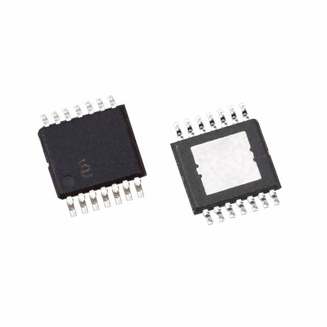
The EL5412 is available in both the 14-pin TSSOP and 14pin HTSSOP packages and features a standard operational
amplifier pinout. They are specified for operation over the full
-40°C to +85°C temperature range.
Ordering Information
PART
NUMBER
• 40MHz -3dB bandwidth
• Supply voltage = 4.5V to 16.5V
• Low supply current (per amplifier) = 2.5mA
• High slew rate = 55V/µs
• Unity-gain stable
• Rail-to-rail output swing
• ±190mA output short current
• Pb-Free Available (RoHS Compliant)
Applications
• TFT-LCD panels
• VCOM amplifiers
• Drivers for A-to-D converters
• Data acquisition
• Video processing
• Audio processing
PACKAGE
TAPE &
REEL
PKG. DWG. #
EL5412IR
14-Pin TSSOP
-
MDP0044
EL5412IR-T7
14-Pin TSSOP
7”
MDP0044
EL5412IR-T13
14-Pin TSSOP
13”
MDP0044
EL5412IRZ
(See Note)
14-Pin TSSOP
(Pb-free)
-
MDP0044
EL5412IRZ-T7
(See Note)
14-Pin TSSOP
(Pb-free)
7”
MDP0044
EL5412IRZ-T13
(See Note)
14-Pin TSSOP
(Pb-free)
13”
MDP0044
EL5412IRE
14-Pin HTSSOP
-
MDP0048
EL5412IRE-T7
14-Pin HTSSOP
7”
MDP0048
VINA- 2
EL5412IRE-T13
14-Pin HTSSOP
13”
MDP0048
VINA+ 3
NOTE: Intersil Pb-free products employ special Pb-free material sets;
molding compounds/die attach materials and 100% matte tin plate
termination finish, which are RoHS compliant and compatible with
both SnPb and Pb-free soldering operations. Intersil Pb-free products
are MSL classified at Pb-free peak reflow temperatures that meet or
exceed the Pb-free requirements of IPC/JEDEC J STD-020C.
FN7394 Rev 1.00
December 22, 2004
• Active filters
• Test equipment
• Battery-powered applications
• Portable equipment
Pinout
EL5412
(14-PIN TSSOP, 14-PIN HTSSOP)
TOP VIEW
VOUTA 1
14 VOUTD
13 VIND+
+
VS+ 4
11 VS-
VINB+ 5
VINB- 6
VOUTB 7
12 VIND+
10 VINC+
+
-
+
-
9 VINC8 VOUTC
Page 1 of 8
�EL5412
Absolute Maximum Ratings (TA = 25°C)
Supply Voltage between VS+ and VS- . . . . . . . . . . . . . . . . . . . .+18V
Input Voltage . . . . . . . . . . . . . . . . . . . . . . . . . . . VS- -0.5V, VS +0.5V
Maximum Continuous Output Current . . . . . . . . . . . . . . . . . . . 65mA
Maximum Die Temperature . . . . . . . . . . . . . . . . . . . . . . . . . . +125°C
Storage Temperature . . . . . . . . . . . . . . . . . . . . . . . .-65°C to +150°C
Ambient Operating Temperature . . . . . . . . . . . . . . . .-40°C to +85°C
Power Dissipation . . . . . . . . . . . . . . . . . . . . . . . . . . . . . See Curves
CAUTION: Stresses above those listed in “Absolute Maximum Ratings” may cause permanent damage to the device. This is a stress only rating and operation of the
device at these or any other conditions above those indicated in the operational sections of this specification is not implied.
IMPORTANT NOTE: All parameters having Min/Max specifications are guaranteed. Typ values are for information purposes only. Unless otherwise noted, all tests are
at the specified temperature and are pulsed tests, therefore: TJ = TC = TA
Electrical Specifications
PARAMETER
VS+ = +5V, VS- = -5V, RL = 1k to 0V, TA = 25°C, unless otherwise specified.
DESCRIPTION
CONDITIONS
MIN
TYP
MAX
UNIT
3
15
mV
INPUT CHARACTERISTICS
VOS
Input Offset Voltage
TCVOS
Average Offset Voltage Drift (Note 1)
IB
Input Bias Current
RIN
Input Impedance
1
G
CIN
Input Capacitance
2
pF
CMIR
Common-Mode Input Range
CMRR
Common-Mode Rejection Ratio
for VIN from -5.5V to 5.5V
50
70
dB
AVOL
Open-Loop Gain
-4.5V VOUT 4.5V
60
74
dB
VCM = 0V
7
VCM = 0V
2
-5.5
µV/°C
60
+5.5
nA
V
OUTPUT CHARACTERISTICS
VOL
Output Swing Low
IL = -5mA
VOH
Output Swing High
IL = 5mA
ISC
IOUT
-4.92
4.85
-4.85
V
4.92
V
Short-circuit Current
±195
mA
Output Current
±65
mA
80
dB
POWER SUPPLY PERFORMANCE
PSRR
Power Supply Rejection Ratio
VS is moved from ±2.25V to ±7.75V
IS
Supply Current (Per Amplifier)
No load
2.5
60
3.75
mA
DYNAMIC PERFORMANCE
SR
Slew Rate (Note 2)
-4.0V VOUT 4.0V, 20% to 80%
55
V/µs
tS
Settling to +0.1% (AV = +1)
(AV = +1), VO = 2V Step
120
ns
BW
-3dB Bandwidth
40
MHz
GBWP
Gain-Bandwidth Product
22
MHz
PM
Phase Margin
52
°
CS
Channel Separation
f = 5MHz
110
dB
dG
Differential Gain (Note 3)
RF = RG = 1kand VOUT = 1.4V
0.12
%
dP
Differential Phase (Note 3)
RF = RG = 1kand VOUT = 1.4V
0.17
°
NOTES:
1. Measured over operating temperature range
2. Slew rate is measured on rising and falling edges
3. NTSC signal generator used
FN7394 Rev 1.00
December 22, 2004
Page 2 of 8
�EL5412
Electrical Specifications
PARAMETER
VS+ = +5V, VS- = 0V, RL = 1k to 2.5V, TA = 25°C, unless otherwise specified.
DESCRIPTION
CONDITION
MIN
TYP
MAX
UNIT
3
15
mV
INPUT CHARACTERISTICS
VOS
Input Offset Voltage
TCVOS
Average Offset Voltage Drift (Note 1)
IB
Input Bias Current
RIN
Input Impedance
1
G
CIN
Input Capacitance
2
pF
CMIR
Common-Mode Input Range
CMRR
Common-Mode Rejection Ratio
for VIN from -0.5V to 5.5V
45
66
dB
AVOL
Open-Loop Gain
0.5V VOUT 4.5V
60
74
dB
VCM = 2.5V
7
VCM = 2.5V
2
-0.5
µV/°C
60
+5.5
nA
V
OUTPUT CHARACTERISTICS
VOL
Output Swing Low
IL = -5mA
VOH
Output Swing High
IL = 5mA
ISC
IOUT
80
4.85
150
mV
4.92
V
Short-circuit Current
±195
mA
Output Current
±65
mA
80
dB
POWER SUPPLY PERFORMANCE
PSRR
Power Supply Rejection Ratio
VS is moved from 4.5V to 15.5V
IS
Supply Current (Per Amplifier)
No Load
2.5
60
3.75
mA
DYNAMIC PERFORMANCE
SR
Slew Rate (Note 2)
1V VOUT 4V, 20% o 80%
55
V/µs
tS
Settling to +0.1% (AV = +1)
(AV = +1), VO = 2V Step
120
ns
BW
-3dB Bandwidth
40
MHz
GBWP
Gain-Bandwidth Product
22
MHz
PM
Phase Margin
52
°
CS
Channel Separation
f = 5MHz
110
dB
dG
Differential Gain (Note 3)
RF = RG = 1k and VOUT = 1.4V
0.30
%
dP
Differential Phase (Note 3)
RF = RG = 1k and VOUT = 1.4V
0.66
°
NOTES:
1. Measured over operating temperature range
2. Slew rate is measured on rising and falling edges
3. NTSC signal generator used
FN7394 Rev 1.00
December 22, 2004
Page 3 of 8
�EL5412
Electrical Specifications
PARAMETER
VS+ = +15V, VS- = 0V, RL = 1k to 7.5V, TA = 25°C, unless otherwise specified.
DESCRIPTION
CONDITION
MIN
TYP
MAX
UNIT
3
15
mV
INPUT CHARACTERISTICS
VOS
Input Offset Voltage
TCVOS
Average Offset Voltage Drift (Note 1)
IB
Input Bias Current
RIN
Input Impedance
1
G
CIN
Input Capacitance
2
pF
CMIR
Common-Mode Input Range
CMRR
Common-Mode Rejection Ratio
for VIN from -0.5V to 15.5V
53
72
dB
AVOL
Open-Loop Gain
0.5V VOUT 14.5V
60
74
dB
VCM = 7.5V
7
VCM = 7.5V
2
-0.5
µV/°C
60
+15.5
nA
V
OUTPUT CHARACTERISTICS
VOL
Output Swing Low
IL = -7.5mA
VOH
Output Swing High
IL = 7.5mA
ISC
Short-circuit Current
IOUT
Output Current
80
150
mV
14.85
14.92
V
±180
±195
mA
±65
mA
80
dB
POWER SUPPLY PERFORMANCE
PSRR
Power Supply Rejection Ratio
VS is moved from 4.5V to 15.5V
IS
Supply Current (Per Amplifier)
No Load
2.5
60
3.75
mA
DYNAMIC PERFORMANCE
SR
Slew Rate (Note 2)
1V VOUT 14V, 20% o 80%
55
V/µs
tS
Settling to +0.1% (AV = +1)
(AV = +1), VO = 2V Step
120
ns
BW
-3dB Bandwidth
40
MHz
GBWP
Gain-Bandwidth Product
22
MHz
PM
Phase Margin
52
°
CS
Channel Separation
f = 5MHz
110
dB
dG
Differential Gain (Note 3)
RF = RG = 1k and VOUT = 1.4V
0.10
%
dP
Differential Phase (Note 3)
RF = RG = 1k and VOUT = 1.4V
0.11
°
NOTES:
1. Measured over operating temperature range
2. Slew rate is measured on rising and falling edges
3. NTSC signal generator used
FN7394 Rev 1.00
December 22, 2004
Page 4 of 8
�EL5412
Typical Performance Curves
Typical
Production
Distortion
300
200
100
VS=±5V
15
10
5
FIGURE 1. INPUT OFFSET VOLTAGE DISTRIBUTION
0.008
INPUT BIAS CURRENT (µA)
INPUT OFFSET VOLTAGE (mV)
4
3
2
1
30
70
110
150
21
19
17
15
13
11
VS=±5V
0.004
0
-0.004
-0.008
-0.012
-50
-10
30
70
110
150
TEMPERATURE (°C)
TEMPERATURE (°C)
FIGURE 3. INPUT OFFSET VOLTAGE vs TEMPERATURE
FIGURE 4. INPUT BIAS CURRENT vs TEMPERATURE
VS=±5V
IOUT=5mA
4.96
4.95
4.94
-50
0
50
100
150
TEMPERATURE (°C)
FIGURE 5. OUTPUT HIGH VOLTAGE vs TEMPERATURE
FN7394 Rev 1.00
December 22, 2004
OUTPUT LOW VOLTAGE (V)
-4.91
4.97
OUTPUT HIGH VOLTAGE (V)
9
FIGURE 2. INPUT OFFSET VOLTAGE DRIFT
5
-10
7
1
8
10
6
4
2
-0
-2
-4
-6
-8
-10
-12
12
INPUT OFFSET VOLTAGE DRIFT, TCVOS (µV/°C)
INPUT OFFSET VOLTAGE (mV)
0
-50
5
0
0
4.93
Typical
Production
Distortion
20
3
400
25
VS=±5V
TA=25°C
QUANTITY (AMPLIFIERS)
QUANTITY (AMPLIFIERS)
500
-4.92
VS=±5V
IOUT=-5mA
-4.93
-4.94
-4.95
-4.96
-4.97
-50
0
50
100
150
TEMPERATURE (°C)
FIGURE 6. OUTPUT LOW VOLTAGE vs TEMPERATURE
Page 5 of 8
�EL5412
Typical Performance Curves
MEASURED CHANNEL A to D or B to C
OTHER COMBINATIONS YIELD IMPROVED
REJECTION
-60
XTALK (dB)
-80
VS=±5V
RL=1k
AV=1
VIN=110mVRMS
-100
-120
-140
-160
1K
10K
100K
1M
10M 30M
FREQUENCY (Hz)
FIGURE 7. CHANNEL SEPARATION vs FREQUENCY RESPONSE
Pin Descriptions
PIN NO.
PIN NAME
1
VOUTA
PIN FUNCTION
EQUIVALENT CIRCUIT
Amplifier A Output
VS+
GND
VS-
CIRCUIT 1
2
VINA-
Amplifier A Inverting Input
VS+
CIRCUIT 2
3
VINA+
4
VS+
5
VINB+
Amplifier B Non-Inverting Input
(Reference Circuit 2)
6
VINB-
Amplifier B Inverting Input
(Reference Circuit 2)
7
VOUTB
Amplifier B Output
(Reference Circuit 1)
8
VOUTC
Amplifier C Output
(Reference Circuit 1)
9
VINC-
Amplifier C Inverting Input
(Reference Circuit 2)
10
VINC+
Amplifier C Non-Inverting Input
(Reference Circuit 2)
11
VS-
12
VIND+
Amplifier D Non-Inverting Input
(Reference Circuit 2)
13
VIND-
Amplifier D Inverting Input
(Reference Circuit 2)
14
VOUTD
Amplifier D Output
(Reference Circuit 1)
FN7394 Rev 1.00
December 22, 2004
Amplifier A Non-Inverting Input
VS-
(Reference Circuit 2)
Positive Power Supply
Negative Power Supply
Page 6 of 8
�EL5412
Applications Information
Output Phase Reversal
Product Description
The EL5412 voltage feedback amplifier is fabricated using a
high voltage CMOS process. It exhibits rail-to-rail input and
output capability, is unity gain stable and has low power
consumption (2.5mA per amplifier). These features make
the EL5412 ideal for a wide range of general-purpose
applications. Connected in voltage follower mode and driving
a load of 2k, the EL5412 has a -3dB bandwidth of 40MHz
while maintaining a 55V/µs slew rate. The EL5412 is a quad
amplifier.
The EL5412 is immune to phase reversal as long as the
input voltage is limited from VS- -0.5V to VS+ +0.5V. Figure 9
shows a photo of the output of the device with the input
voltage driven beyond the supply rails. Although the device's
output will not change phase, the input's overvoltage should
be avoided. If an input voltage exceeds supply voltage by
more than 0.6V, electrostatic protection diodes placed in the
input stage of the device begin to conduct and overvoltage
damage could occur.
VS=±2.5V, TA=25°C, AV=1, VIN=6VP-P
1V
Operating Voltage, Input, and Output
The EL5412 is specified with a single nominal supply voltage
from 5V to 15V or a split supply with its total range from 5V
to 15V. Correct operation is guaranteed for a supply range of
4.5V to 16.5V. Most EL5412 specifications are stable over
both the full supply range and operating temperatures of
-40°C to +85°C. Parameter variations with operating voltage
and/or temperature are shown in the typical performance
curves.
The input common-mode voltage range of the EL5412
extends 500mV beyond the supply rails. The output swings
of the EL5412 typically extend to within 100mV of positive
and negative supply rails with load currents of 5mA.
Decreasing load currents will extend the output voltage
range even closer to the supply rails. Figure 8 shows the
input and output waveforms for the device in the unity-gain
configuration. Operation is from ±5V supply with a 1k load
connected to GND. The input is a 10VP-P sinusoid. The
output voltage is approximately 9.8VP-P.
VS=±5V, TA=25°C, AV=1, VIN=10VP-P
5V
10µs
1V
FIGURE 9. OPERATION WITH BEYOND-THE-RAILS INPUT
Power Dissipation
With the high-output drive capability of the EL5412 amplifier,
it is possible to exceed the 125°C 'absolute-maximum
junction temperature' under certain load current conditions.
Therefore, it is important to calculate the maximum junction
temperature for the application to determine if load
conditions need to be modified for the amplifier to remain in
the safe operating area.
The maximum power dissipation allowed in a package is
determined according to:
10µs
5V
OUTPUT
INPUT
T JMAX – T AMAX
P DMAX = -------------------------------------------- JA
where:
• TJMAX = Maximum junction temperature
• TAMAX = Maximum ambient temperature
• JA = Thermal resistance of the package
• PDMAX = Maximum power dissipation in the package
FIGURE 8. OPERATION WITH RAIL-TO-RAIL INPUT AND
OUTPUT
Output Current Driving Capability
The EL5412 will limit the short-circuit current to ±190mA if
the output is directly shorted to the positive or the negative
supply. If an output is shorted indefinitely, the power
dissipation could easily increase such that the device may
be damaged. Maximum reliability is maintained if the output
continuous current never exceeds ±65mA. This limit is set by
the design of the internal metal interconnects.
FN7394 Rev 1.00
December 22, 2004
The maximum power dissipation actually produced by an IC
is the total quiescent supply current times the total power
supply voltage, plus the power in the IC due to the loads, or:
P DMAX = i V S I SMAX + V S + – V OUT i I LOAD i
when sourcing, and:
P DMAX = i V S I SMAX + V OUT i – V S - I LOAD i
when sinking.
Page 7 of 8
�EL5412
Where:
PACKAGE MOUNTED ON A JEDEC JESD51-3
LOW EFFECTIVE THERMAL CONDUCTIVITY
TEST BOARD
• i = Channel 1 to 4
• VS = Total supply voltage
• ISMAX = Maximum supply current per amplifier
• VOUTi = Maximum output voltage of the application
• ILOADi = Load current
If we set the two PDMAX equations equal to each other, we
can solve for RLOADi to avoid device overheat. Figure 10
and Figure 11 provide a convenient way to see if the device
will overheat. The maximum safe power dissipation can be
found graphically, based on the package type and the
ambient temperature. By using the previous equation, it is a
simple matter to see if PDMAX exceeds the device's power
derating curves. To ensure proper operation, it is important
to observe the recommended derating curves shown in
Figures 10 and 11.
JEDEC JESD51-7 HIGH EFFECTIVE THERMAL
CONDUCTIVITY TEST BOARD - HTSSOP
EXPOSED DIEPAD SOLDERED TO PCB PER
JESD51-5
POWER DISSIPATION (W)
3.5
3
MAX
TJ=125°C
2.632W
2.5
2
1.5
1.0W
1
J
0
O
38 P 14
°C
/W
TSS
O
A =10
0.5
0
25
50
MAX
TJ=125°C
1000
800
694mW
HT
SS
O
14 P 14
4°
C/
W
TS
SO
J
P
14
A =1
65
°C
/W
600
JA =
606mW
400
200
0
0
25
50
75 85 100
125
150
AMBIENT TEMPERATURE (°C)
FIGURE 11. PACKAGE POWER DISSIPATION vs AMBIENT
TEMPERATURE
Unused Amplifiers
It is recommended that any unused amplifiers be configured
as a unity gain follower. The inverting input should be directly
connected to the output and the non-inverting input tied to
the ground plane.
Power Supply Bypassing and Printed Circuit
Board Layout
HT
SS
JA
=
POWER DISSIPATION (mW)
1200
P14
0°C
/W
75 85 100
125
150
AMBIENT TEMPERATURE (°C)
FIGURE 10. PACKAGE POWER DISSIPATION vs AMBIENT
TEMPERATURE
The EL5412 can provide gain at high frequency. As with any
high-frequency device, good printed circuit board layout is
necessary for optimum performance. Ground plane
construction is highly recommended, lead lengths should be
as short as possible and the power supply pins must be well
bypassed to reduce the risk of oscillation. For normal single
supply operation, where the VS- pin is connected to ground,
a 0.1µF ceramic capacitor should be placed from VS+ to pin
to VS- pin. A 4.7µF tantalum capacitor should then be
connected in parallel, placed in the region of the amplifier.
One 4.7µF capacitor may be used for multiple devices. This
same capacitor combination should be placed at each
supply pin to ground if split supplies are to be used.
© Copyright Intersil Americas LLC 2003-2004. All Rights Reserved.
All trademarks and registered trademarks are the property of their respective owners.
For additional products, see www.intersil.com/en/products.html
Intersil products are manufactured, assembled and tested utilizing ISO9001 quality systems as noted
in the quality certifications found at www.intersil.com/en/support/qualandreliability.html
Intersil products are sold by description only. Intersil may modify the circuit design and/or specifications of products at any time without notice, provided that such
modification does not, in Intersil's sole judgment, affect the form, fit or function of the product. Accordingly, the reader is cautioned to verify that datasheets are
current before placing orders. Information furnished by Intersil is believed to be accurate and reliable. However, no responsibility is assumed by Intersil or its
subsidiaries for its use; nor for any infringements of patents or other rights of third parties which may result from its use. No license is granted by implication or
otherwise under any patent or patent rights of Intersil or its subsidiaries.
For information regarding Intersil Corporation and its products, see www.intersil.com
FN7394 Rev 1.00
December 22, 2004
Page 8 of 8
�


 工商网监
湘ICP备2023018690号
工商网监
湘ICP备2023018690号
