DATASHEET
EL9110
FN7305
Rev 5.00
November 30, 2007
Differential Receiver/Equalizer
The EL9110 is a single channel differential receiver and
equalizer. It contains a high speed differential receiver with 5
programmable poles. The outputs of these pole blocks are
then summed into an output buffer. The equalization length
is set with the voltage on a single pin. The EL9110 also
contains a three-statable output, enabling multiple devices to
be connected in parallel and used in a multiplexing
application.
The gain can be adjusted up or down by 6dB using the
VGAIN control signal. In addition, a further 6dB of gain can
be switched in to provide a matched drive into a cable.
Features
• 150MHz -3dB bandwidth
• CAT-5 compensation
- 75MHz @ 1000ft
- 125MHz @ 500ft
• 33mA supply current
• Differential input range 3.2V
• Common mode input range ±4.5V
• ±5V supply
The EL9110 has a bandwidth of 150MHz and consumes just
33mA on ±5V supply. A single input voltage is used to set the
compensation levels for the required length of cable.
• Output to within 1.5V of supplies
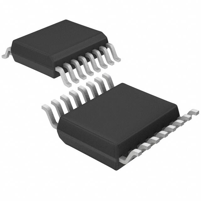
The EL9110 is available in the 16 Ld QSOP package and is
specified for operation over the full -40°C to +85°C
temperature range.
• Pb-free available (RoHS compliant)
• Available in 16 Ld QSOP package
Applications
• Twisted-pair receiving/equalizer
Ordering Information
PART
NUMBER
PART
MARKING
• KVM (Keyboard/Video/Mouse)
PACKAGE
PKG. DWG. #
• VGA over twisted-pair
EL9110IU
9110IU
16 Ld QSOP
MDP0040
• Security video
EL9110IU-T7*
9110IU
16 Ld QSOP
MDP0040
Pinout
EL9110IU-T13*
9110IU
16 Ld QSOP
MDP0040
EL9110IUZ
(Note)
9110IUZ
16 Ld QSOP
(Pb-free)
MDP0040
EL9110IUZ-T7*
(Note)
9110IUZ
16 Ld QSOP
(Pb-free)
MDP0040
EL9110IUZ-T13* 9110IUZ
(Note)
16 Ld QSOP
(Pb-free)
MDP0040
*Please refer to TB347 for details on reel specifications.
NOTE: These Intersil Pb-free plastic packaged products employ
special Pb-free material sets; molding compounds/die attach
materials and 100% matte tin plate PLUS ANNEAL - e3 termination
finish, which is RoHS compliant and compatible with both SnPb and
Pb-free soldering operations. Intersil Pb-free products are MSL
classified at Pb-free peak reflow temperatures that meet or exceed
the Pb-free requirements of IPC/JEDEC J STD-020.
FN7305 Rev 5.00
November 30, 2007
EL9110
(16 LD QSOP)
TOP VIEW
CTRL_REF 1
VCTRL 2
16 CMEXT
15 VS+
VINP 3
14 ENBL
VINM 4
13 VSA+
VS- 5
12 VOUT
CMOUT 6
11 VSA-
VGAIN 7
10 0V
LOGIC_REF 8
9 X2
Page 1 of 10
�EL9110
Absolute Maximum Ratings (TA = +25°C)
Thermal Information
Supply Voltage between VS+ and VS- . . . . . . . . . . . . . . . . . . . . .12V
Maximum Continuous Output Current . . . . . . . . . . . . . . . . . . . 30mA
Pin Voltages . . . . . . . . . . . . . . . . . . . . . . . . . VS- -0.5V to VS+ +0.5V
Power Dissipation . . . . . . . . . . . . . . . . . . . . . . . . . . . . . See Curves
Storage Temperature . . . . . . . . . . . . . . . . . . . . . . . .-65°C to +150°C
Ambient Operating Temperature . . . . . . . . . . . . . . . .-40°C to +85°C
Die Junction Temperature . . . . . . . . . . . . . . . . . . . . . . . . . . . +150°C
Pb-free reflow profile . . . . . . . . . . . . . . . . . . . . . . . . . .see link below
http://www.intersil.com/pbfree/Pb-FreeReflow.asp
CAUTION: Do not operate at or near the maximum ratings listed for extended periods of time. Exposure to such conditions may adversely impact product reliability and
result in failures not covered by warranty.
IMPORTANT NOTE: All parameters having Min/Max specifications are guaranteed. Typ values are for information purposes only. Unless otherwise noted, all tests are
at the specified temperature and are pulsed tests, therefore: TJ = TC = TA
Electrical Specifications
PARAMETER
VSA+ = VA+ = +5V, VSA- = VA- = -5V, TA = +25°C, Unless Otherwise Specified
DESCRIPTION
CONDITIONS
MIN
(Note 1)
MAX
(Note 1)
TYP
UNIT
AC PERFORMANCE
BW
Bandwidth
(See Figure 1)
150
MHz
SR
Slew Rate
VIN = -1V to +1V, VG = 0.35, VC = 0, RL = 75 + 75
1.5
V/ns
THD
Total Harmonic Distortion
10MHz 1VP-P out, VG = 0.35V, X2 gain, VC = 0
-50
dBc
DC PERFORMANCE
VOS
Offset Voltage (bin #1)
X2 gain, no equalization
-250
Offset Voltage (bin #2)
-10
+250
mV
CPI9049
mV
INPUT CHARACTERISTICS
CMIR
Common-mode Input Range
Common-mode extension off
-4/+3.5
V
CMIRx
Extended CMIR
Common-mode extension on
±4.5
V
ONOISE
Output Noise
VG = 0.35, X2 gain, 75 + 75 load, VC = 0.6
25
mV
RMS
CMRR
Common-mode Rejection Ratio
Measured at 10kHz
60
dB
CMRR+
Common-mode Rejection Ratio
Measured at 10MHz
50
dB
CMBW
CM Amplifier Bandwidth
10K || 10pF load
50
MHz
CMSLEW
CM Slew Rate
Measured @ +1V to -1V
100
V/µs
CINDIFF
Differential Input Capacitance
Capacitance VINP to VINM
RINDIFF
Differential Input Resistance
Resistance VINP to VINM
CINCM
CM Input Capacitance
Capacitance VINP = VINM to ground
RINCM
CM Input Resistance
Resistance VINP = VINM to ground
+IIN
Positive Input Current
-IIN
VINDIFF
600
fF
2.4
M
1.2
pF
2.8
M
DC bias @ VINP = VINM = 0V
1
µA
Negative Input Current
DC bias @ VINP = VINM = 0V
1
µA
Differential Input Range
VINP - VINM when slope gain falls to 0.9
3.2
V
1
1
2.5
OUTPUT CHARACTERISTICS
VO
Output Voltage Swing
RL = 150
IOUT
Output Drive Current
RL = 10, VINP = 1V, VINM = 0V, X2 = gain,
VG = 0.35
ROUTCM
CM Output Resistance
at 100kHz
DiffGain
Differential Gain
VC = 0, VG = 0.35, X2 = 5, RL = 75 + 75
ISON
Supply Current
VENBL = 5, VINM = 0
27
38
mA
ISOFF
Supply Current
VENBL = 0, VINM = 0
0.4
0.8
mA
50
0.85
±3.5
V
60
mA
30
1.0
1.1
SUPPLY
FN7305 Rev 5.00
November 30, 2007
Page 2 of 10
�EL9110
Electrical Specifications
PARAMETER
PSRR
VSA+ = VA+ = +5V, VSA- = VA- = -5V, TA = +25°C, Unless Otherwise Specified (Continued)
DESCRIPTION
MIN
(Note 1)
CONDITIONS
Power Supply Rejection Ratio
DC to 100kHz, ±5V supply
TYP
MAX
(Note 1)
60
UNIT
dB
LOGIC CONTROL PINS
VHI
Logic High Level
VIN - VLOGIC ref for guaranteed high level
VLOW
Logic Low Level
VIN - VLOGIC ref for guaranteed low level
0.8
V
ILOGICH
Logic High Input Current
VIN = 5V, VLOGIC = 0V
50
µA
ILOGICL
Logic Low Input Current
VIN = 0V, VLOGIC = 0V
15
µA
1.35
V
NOTE:
1. Parts are 100% tested at +25°C. Over-temperature limits established by characterization and are not production tested.
Pin Descriptions
PIN NUMBER
PIN NAME
PIN TYPE
1
CTRL_REF
Input
Reference voltage for VGAIN and VCTRL pins
2
VCTRL
Input
Control voltage (0 to 1V) to set equalization
3
VINP
Input
Positive differential input
4
VINM
Input
Negative differential input
5
VS-
Power
-5V to core of chip
6
CMOUT
Output
Output of common mode voltage present at inputs
7
VGAIN
Input
Control voltage to set overall gain (0V to 1V)
8
LOGIC_REF
Input
Reference voltage for all logic signals
9
X2
Logic Input
10
0V
11
VSA-
Power
-5V to output buffer
12
VOUT
Output
Single-ended output voltage reference to pin 10
13
VSA+
Power
+5V to output buffer
14
ENBL
Logic Input
15
VS+
Power
16
CMEXT
Logic Input
FN7305 Rev 5.00
November 30, 2007
PIN FUNCTION
Logic signal; low - gain = 1, high - gain = 2
0V reference for output voltage
Logic signal to enable pin; low - disabled, high - enabled
+5V to core of chip
Logic signal to enable CM range extension; active high
Page 3 of 10
�EL9110
Typical Performance Curves
5
-45
THD (dBc)
3
GAIN (dB)
-40
VGAIN = 0V
VCTRL = 0V
RLOAD = 150
X2 = OFF
1
-1
-3
-50
VGAIN = 0V
VCTRL = 0V
VSS = +5V
VEE = -5V
RLOAD = 150
X2 = OFF
INPUT = 0dBm
-55
-60
-5
1M
10M
-65
0.1M
100M
1M
FREQUENCY (Hz)
10M
100M
FREQUENCY (Hz)
FIGURE 1. FREQUENCY RESPONSE
FIGURE 2. TOTAL HARMONIC DISTORTION
0
200mV/DIV
CMRR (dBc)
-20
VCTR = 0V
VGAIN = 0.35V
X2 = ON
-40
-60
-80
-100
100k
2ns/DIV
1M
10M
100M
FREQUENCY (Hz)
FIGURE 3. RISE TIME
GAIN (dB)
2
-20
VGAIN = 0.35V
VCTRL = 0V
RLOAD = 150
X2 = ON
-40
-PSRR (dB)
4
FIGURE 4. COMMON MODE REJECTION
0
-2
1M
10M
100M
FREQUENCY (Hz)
FIGURE 5. CM AMPLIFIER BANDWIDTH
FN7305 Rev 5.00
November 30, 2007
-60
-80
-100
-4
-6
100k
VEE = -5V
VCTRL = 0V
VGAIN = 0V
INPUTS ON GND
-120
10
100
1k
10k
100k
1M
10M
100M
FREQUENCY (Hz)
FIGURE 6. PSRR vs FREQUENCY
Page 4 of 10
�EL9110
Typical Performance Curves (Continued)
0
10dB/DIV
60
50
VCTR = 800mV
40
GAIN (dB)
+PSRR (dB)
-20
VCC = 5V
VCTRL = 0V
VGAIN = 0V
INPUTS ON GND
-40
-60
30
20
10
0
-10
-80
-20
-100
10
100
1k
10k
100k
1M
10M
10M
1M
100M
FIGURE 7. PSRR vs FREQUENCY
10ns/DIV
VCTRL = 0mV
-10
-30
JEDEC JESD51-3 LOW EFFECTIVE THERMAL
CONDUCTIVITY TEST BOARD
1.4
POWER DISSIPATION (W)
GROUP DELAY (ns)
FIGURE 8. GAIN AS THE FUNCTION OF VCTRL
30
10
100M
FREQUENCY (Hz)
FREQUENCY (Hz)
50
VCTRL = 0mV
100mV STEP
VCTRL = 900mV
1.2
1
791mW
0.8
J
0.6
QS
O
P1
6
58
°C
/W
A =1
0.4
0.2
100mV STEP
-50
1M
10M
0
100M 200M
0
25
FREQUENCY (Hz)
75 85 100
125
150
AMBIENT TEMPERATURE (°C)
FIGURE 10. PACKAGE POWER DISSIPATION vs AMBIENT
TEMPERATURE
FIGURE 9. GROUP DELAY AS THE FUNCTION OF THE
FREQUENCY REPONSE CONTROL VOLTAGE
(VCTRL)
1.8
POWER DISSIPATION (W)
50
JEDEC JESD51-7 HIGH EFFECTIVE THERMAL
CONDUCTIVITY TEST BOARD
1.6
1.4
1.2 1.116W
1
J
0.8
0.6
QS
OP
16
12
°C
/W
A =1
0.4
0.2
0
0
25
50
75 85 100
125
150
AMBIENT TEMPERATURE (°C)
FIGURE 11. PACKAGE POWER DISSIPATION vs AMBIENT TEMPERATURE
FN7305 Rev 5.00
November 30, 2007
Page 5 of 10
�EL9110
Applications Information
Logic Control
The EL9110 has three logical input pins, Chip Enable
(ENBL), Common Mode Extend (CMEXT), and Switch Gain
(X2). The logic circuits all have a nominal threshold of 1.1V
above the potential of the logic reference pin. In most
applications it is expected that this chip will run from a +5V,
0V, -5V supply system with logic being run between 0V and
+5V. In this case the logic reference voltage should be tied to
the 0V supply. If the logic is referenced to the -5V rail, then
the logic reference should be connected to -5V. The logic
reference pin sources about 60µA and this will rise to about
200µA if all inputs are true (positive).
The logic inputs all source up to 10µA when they are held at
the logic reference level. When taken positive, the inputs
sink a current dependent on the high level, up to 50µA for a
high level 5V above the reference level.
The logic inputs, if not used, should be tied to the
appropriate voltage in order to define their state.
Control Reference and Signal Reference
Analog control voltages are required to set the equalizer and
contrast levels. These signals are voltages in the range 0V
to 1V, which are referenced to the control reference pin. It is
expected that the control reference pin will be tied to 0V and
the control voltage will vary from 0V to 1V. It is; however,
acceptable to connect the control reference to any potential
between -5V and 0V to which the control voltages are
referenced.
The control voltage pins themselves are high impedance.
The control reference pin will source between 0µA and
200µA depending on the control voltages being applied.
The control reference and logic reference effectively remove
the necessity for the 0V rail and operation from ±5V (or 0V
and 10V) only is possible. However we still need a further
reference to define the 0V level of the single ended output
signal. The reference for the output signal is provided by the
0V pin. The output stage cannot pull fully up or down to
either supply so it is important that the reference is
positioned to allow full output swing. The 0V reference
should be tied to a 'quiet ground' as any noise on this pin is
transferred directly to the output. The 0V pin is a high
impedance pin and draws dc bias currents of a few µA and
similar levels of AC current.
Common Mode Extension
The common mode extension circuitry extends the range of
input common mode voltage before the input differential
amplifier is overloaded. It does this by reducing the voltage
equally at both inputs of the first differential amplifier as the
common mode signal rises towards the supply. Similarly,
when the common mode input signal goes low, the inputs to
the first differential amplifier are raised whilst preserving the
FN7305 Rev 5.00
November 30, 2007
differential signal and maintain the amplifier within its
common mode operating range.
This operation may not always be desirable. A problem
occurs because the EL9110 sinks or sources a common
mode current though its input pins to create the common
mode offset voltage. Assuming the system has been set up
so that the differential line has a well-balanced impedance,
then a problem will only occur when the common mode
impedance to ground is not low. This will occur in systems
where the inputs to the EL9110 are AC coupled. In such
systems it is recommended that the common mode
extension be disabled. In systems where the differential
input signal is directly coupled and has its common mode
level defined by a low impedance line driver, the common
mode extension circuitry can extend the total common mode
range by 2V to 3V.
Equalizing
When transmitting a signal across a twisted pair cable, it is
found that the high frequency (above 1MHz) information is
attenuated more significantly than the information at low
frequencies. The attenuation is predominantly due to
resistive skin effect losses and has a loss curve which
depends on the resistivity of the conductor, surface condition
of the wire and the wire diameter. For the range of high
performance twisted pair cables based on 24awg copper
wire (Cat 5 etc.) these parameters vary only a little between
cable types, and in general cables exhibit the same
frequency dependence of loss. (The lower loss cables can
be compared with somewhat longer lengths of their more
lossy brothers.) This enables a single equalizing law
equation to be built into the EL9110.
With a control voltage applied between pins 2 and 1, the
frequency dependence of the equalization is shown in
Figure 8. The equalization matches the cable loss up to
about 100MHz. Above this, system gain is rolled off rapidly
to reduce noise bandwidth. The roll-off occurs more rapidly
for higher control voltages, thus the system (cable +
equalizer) bandwidth reduces as the cable length increases.
This is desirable, as noise becomes an increasing issue as
the equalization increases.
The cable loss for 100m, 200m, and 300m of CAT 5 cable,
based on manufacturer's loss curves is shown in Figure 14.
Thus:
• 100m requires VC = 0.2V
• 200m requires VC = 0.6V
and:
• 300m requires VC = 1.0V approximately
Contrast
By varying the voltage between pins 7 and 1, the gain of the
signal path can be changed in the ratio 4:1. The gain change
varies almost linearly with control voltage. For normal
Page 6 of 10
�EL9110
operation it is anticipated the X2 mode will be selected and
the output load will be back matched. A unity gain to the
output load will then be achieved with a gain control voltage
of about 0.35V. This allows the gain to be trimmed up or
down by 6dB to compensate for any gain/loss errors that
affect the contrast of the video signal. Figure 12 shows an
example plot of the gain to the load with gain control voltage.
1.8
GAIN (V)
1.6
1.4
1.2
1.0
0.8
0.6
0
0.2
0.4
0.6
0.8
1.0
VGAIN
FIGURE 12. VARIATION OF GAIN WITH GAIN CONTROL
VOLTAGE
60
ATTENUATION (dB)
A reflection-free termination is a real "ohmic" resistor with as
less as possible reactive parasitic.
The cable will work as an antenna for all the RF spectrum
which is "in the air" where the cable is used. The spectrum,
particularly its common mode components, could and will
contain high energy level of transients which are above the
built-in protection level of the device and easily could
damage its inputs. Using a transient protection circuit
according to the given application is recommended.
Since the used signal's bandwidth is in the range of 100MHz,
for layout and power supply bypassing the roles of RF
design should be applied.
70
50
The following picture is taken from the DB9110 demoboard's layout. For better visibility the ground plain is
removed.
300M
40
200M
30
The ground plane is shown in Figure 14.
100M
20
50M
10
0
0.01M
The interconnection cable is a transmission line therefore for
proper function it should be treated like transmission line, a
refection-free termination is necessary.
The traces of the layout, up to the point where of the
termination resistor placed, are part of the transmission line
which also includes the cable's connector. A connector with
a better controlled impedance is an obligation for good
picture quality. The termination resistor should be placed
close to the inputs of the device's pins (pin 3 and pin 4.) The
small capacitance differential and common mode
capacitance of the input pins of the device makes it possible
to connect parallel to the termination resistor.
2.0
0.4
Circuit and Layout Recommendation
0.10M
1M
10M
100M
FREQUENCY (Hz)
FIGURE 13. CAT-5 CABLE ATTENUATION CHARACTERISTICS
FIGURE 14. DEMO BOARD LAYOUT
FN7305 Rev 5.00
November 30, 2007
Page 7 of 10
�EL9110
The accompanying circuit diagram is shown in Figure 15.
R11
330
C5
1µF
1 CTRL CMEXT 16
_REF
2 VCTRL
R6
R5
R7
R9
C7
1µF
VS+ 15
3 VINP
ENBL 14
4 VINM
VSA+ 13
5 VS-
VOUT 12
C6
1nF
TP7
6 CMOUT
R12
330
C8
1nF
C10
1µF
VSA- 11
7 VGAIN
0V 10
LOGIC
8
_REF
X2 9
C11
1nF
C9
1µF
FIGURE 15. CIRCUIT DIAGRAM
Block Diagram
CMOUT
DIFFERENTIAL
LINE IN
CMEXT
VS+ VS-
COMMON
MODE RANGE
EXTENDED
BIAS
CIRCUITRY
COMMON
MODE
RECOVERY
X2
LOW FREQ BOOST
VSA+
X2/X1
INPUT AMP
VINP
VINM
LOGICREF
ENBL
CONTRAST
+
VOUT
EQUALIZING
BOOST
0V
±6dB
RANGE
CONTROL
ASP
VCTRL
DIFFERENTIAL TO
SINGLE-ENDED
VSA-
GAIN
ASP
CTRLREF
VGAIN
VS- & VSA- connected
CONNECTED
to -5V
TO -5V
CONNECTED
to +5V
TO +5V
VS+ & VSA+ connected
FN7305 Rev 5.00
November 30, 2007
Page 8 of 10
�EL9110
Typical Application
VCTRL
0.1µF
1 CTRL CMEXT 16
_REF
2 VCTRL
VS+ 15
3 VINP
ENBL 14
4 VINM
VSA+ 13
5 VS-
VOUT 12
+5V
100
-5V
0.1µF
CMOUT
+5V
6 CMOUT
VSA- 11
7 VGAIN
0V 10
LOGIC
_REF
X2 9
8
0.1µF
75
-5V
+5V
0.1µF
FN7305 Rev 5.00
November 30, 2007
Page 9 of 10
�EL9110
Quarter Size Outline Plastic Packages Family (QSOP)
MDP0040
A
QUARTER SIZE OUTLINE PLASTIC PACKAGES FAMILY
D
(N/2)+1
N
INCHES
SYMBOL QSOP16 QSOP24 QSOP28 TOLERANCE NOTES
E
PIN #1
I.D. MARK
E1
1
(N/2)
B
0.010
C A B
e
H
C
SEATING
PLANE
0.007
0.004 C
b
C A B
A
0.068
0.068
0.068
Max.
-
A1
0.006
0.006
0.006
±0.002
-
A2
0.056
0.056
0.056
±0.004
-
b
0.010
0.010
0.010
±0.002
-
c
0.008
0.008
0.008
±0.001
-
D
0.193
0.341
0.390
±0.004
1, 3
E
0.236
0.236
0.236
±0.008
-
E1
0.154
0.154
0.154
±0.004
2, 3
e
0.025
0.025
0.025
Basic
-
L
0.025
0.025
0.025
±0.009
-
L1
0.041
0.041
0.041
Basic
-
N
16
24
28
Reference
Rev. F 2/07
NOTES:
L1
A
1. Plastic or metal protrusions of 0.006” maximum per side are not
included.
2. Plastic interlead protrusions of 0.010” maximum per side are not
included.
c
SEE DETAIL "X"
3. Dimensions “D” and “E1” are measured at Datum Plane “H”.
4. Dimensioning and tolerancing per ASME Y14.5M-1994.
0.010
A2
GAUGE
PLANE
L
A1
4°±4°
DETAIL X
© Copyright Intersil Americas LLC 2003-2007. All Rights Reserved.
All trademarks and registered trademarks are the property of their respective owners.
For additional products, see www.intersil.com/en/products.html
Intersil products are manufactured, assembled and tested utilizing ISO9001 quality systems as noted
in the quality certifications found at www.intersil.com/en/support/qualandreliability.html
Intersil products are sold by description only. Intersil may modify the circuit design and/or specifications of products at any time without notice, provided that such
modification does not, in Intersil's sole judgment, affect the form, fit or function of the product. Accordingly, the reader is cautioned to verify that datasheets are
current before placing orders. Information furnished by Intersil is believed to be accurate and reliable. However, no responsibility is assumed by Intersil or its
subsidiaries for its use; nor for any infringements of patents or other rights of third parties which may result from its use. No license is granted by implication or
otherwise under any patent or patent rights of Intersil or its subsidiaries.
For information regarding Intersil Corporation and its products, see www.intersil.com
FN7305 Rev 5.00
November 30, 2007
Page 10 of 10
�