To our customers,
Old Company Name in Catalogs and Other Documents
On April 1st, 2010, NEC Electronics Corporation merged with Renesas Technology
Corporation, and Renesas Electronics Corporation took over all the business of both
companies. Therefore, although the old company name remains in this document, it is a valid
Renesas Electronics document. We appreciate your understanding.
Renesas Electronics website: http://www.renesas.com
fo ot
r n re
c
ew om
de m
si en
gn d
April 1st, 2010
Renesas Electronics Corporation
Issued by: Renesas Electronics Corporation (http://www.renesas.com)
N
Send any inquiries to http://www.renesas.com/inquiry.
�Notice
3.
4.
5.
6.
7.
“Standard”:
8.
9.
10.
11.
12.
fo ot
r n re
c
ew om
de m
si en
gn d
2.
All information included in this document is current as of the date this document is issued. Such information, however, is
subject to change without any prior notice. Before purchasing or using any Renesas Electronics products listed herein, please
confirm the latest product information with a Renesas Electronics sales office. Also, please pay regular and careful attention to
additional and different information to be disclosed by Renesas Electronics such as that disclosed through our website.
Renesas Electronics does not assume any liability for infringement of patents, copyrights, or other intellectual property rights
of third parties by or arising from the use of Renesas Electronics products or technical information described in this document.
No license, express, implied or otherwise, is granted hereby under any patents, copyrights or other intellectual property rights
of Renesas Electronics or others.
You should not alter, modify, copy, or otherwise misappropriate any Renesas Electronics product, whether in whole or in part.
Descriptions of circuits, software and other related information in this document are provided only to illustrate the operation of
semiconductor products and application examples. You are fully responsible for the incorporation of these circuits, software,
and information in the design of your equipment. Renesas Electronics assumes no responsibility for any losses incurred by
you or third parties arising from the use of these circuits, software, or information.
When exporting the products or technology described in this document, you should comply with the applicable export control
laws and regulations and follow the procedures required by such laws and regulations. You should not use Renesas
Electronics products or the technology described in this document for any purpose relating to military applications or use by
the military, including but not limited to the development of weapons of mass destruction. Renesas Electronics products and
technology may not be used for or incorporated into any products or systems whose manufacture, use, or sale is prohibited
under any applicable domestic or foreign laws or regulations.
Renesas Electronics has used reasonable care in preparing the information included in this document, but Renesas Electronics
does not warrant that such information is error free. Renesas Electronics assumes no liability whatsoever for any damages
incurred by you resulting from errors in or omissions from the information included herein.
Renesas Electronics products are classified according to the following three quality grades: “Standard”, “High Quality”, and
“Specific”. The recommended applications for each Renesas Electronics product depends on the product’s quality grade, as
indicated below. You must check the quality grade of each Renesas Electronics product before using it in a particular
application. You may not use any Renesas Electronics product for any application categorized as “Specific” without the prior
written consent of Renesas Electronics. Further, you may not use any Renesas Electronics product for any application for
which it is not intended without the prior written consent of Renesas Electronics. Renesas Electronics shall not be in any way
liable for any damages or losses incurred by you or third parties arising from the use of any Renesas Electronics product for an
application categorized as “Specific” or for which the product is not intended where you have failed to obtain the prior written
consent of Renesas Electronics. The quality grade of each Renesas Electronics product is “Standard” unless otherwise
expressly specified in a Renesas Electronics data sheets or data books, etc.
Computers; office equipment; communications equipment; test and measurement equipment; audio and visual
equipment; home electronic appliances; machine tools; personal electronic equipment; and industrial robots.
“High Quality”: Transportation equipment (automobiles, trains, ships, etc.); traffic control systems; anti-disaster systems; anticrime systems; safety equipment; and medical equipment not specifically designed for life support.
“Specific”:
Aircraft; aerospace equipment; submersible repeaters; nuclear reactor control systems; medical equipment or
systems for life support (e.g. artificial life support devices or systems), surgical implantations, or healthcare
intervention (e.g. excision, etc.), and any other applications or purposes that pose a direct threat to human life.
You should use the Renesas Electronics products described in this document within the range specified by Renesas Electronics,
especially with respect to the maximum rating, operating supply voltage range, movement power voltage range, heat radiation
characteristics, installation and other product characteristics. Renesas Electronics shall have no liability for malfunctions or
damages arising out of the use of Renesas Electronics products beyond such specified ranges.
Although Renesas Electronics endeavors to improve the quality and reliability of its products, semiconductor products have
specific characteristics such as the occurrence of failure at a certain rate and malfunctions under certain use conditions. Further,
Renesas Electronics products are not subject to radiation resistance design. Please be sure to implement safety measures to
guard them against the possibility of physical injury, and injury or damage caused by fire in the event of the failure of a
Renesas Electronics product, such as safety design for hardware and software including but not limited to redundancy, fire
control and malfunction prevention, appropriate treatment for aging degradation or any other appropriate measures. Because
the evaluation of microcomputer software alone is very difficult, please evaluate the safety of the final products or system
manufactured by you.
Please contact a Renesas Electronics sales office for details as to environmental matters such as the environmental
compatibility of each Renesas Electronics product. Please use Renesas Electronics products in compliance with all applicable
laws and regulations that regulate the inclusion or use of controlled substances, including without limitation, the EU RoHS
Directive. Renesas Electronics assumes no liability for damages or losses occurring as a result of your noncompliance with
applicable laws and regulations.
This document may not be reproduced or duplicated, in any form, in whole or in part, without prior written consent of Renesas
Electronics.
Please contact a Renesas Electronics sales office if you have any questions regarding the information contained in this
document or Renesas Electronics products, or if you have any other inquiries.
N
1.
(Note 1) “Renesas Electronics” as used in this document means Renesas Electronics Corporation and also includes its majorityowned subsidiaries.
(Note 2) “Renesas Electronics product(s)” means any product developed or manufactured by or for Renesas Electronics.
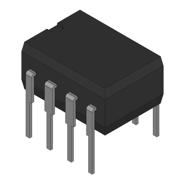
�HA17904 Series
Dual Operational Amplifier
REJ03D0688-0100
(Previous: ADE-204-046)
Rev.1.00
Jun 15, 2005
Description
HA17904 is dual operational amplifier which, provide internal phase compensation and high gain, and mono power
source operation is possible. It can be widely applied to control equipment and to general use.
Features
• Wide range of operating supply voltage and mono power source operation is possible.
• Wide range of common mode input voltage possible to operate with an input around 0V, and output around 0V is
available.
• Frequency characteristics and input bias currrent are temperature compensated.
Ordering Information
Type No.
HA17904PSJ
HA17904FPJ
HA17904FPK
Rev.1.00 Jun 15, 2005 page 1 of 7
Application
Car use
Package Code (Previous Code)
PRDP0008AF-A (DP-8B)
PRSP0008DE-B (FP-8DGV)
PRSP0008DE-B (FP-8DGV)
�HA17904 Series
Pin Arrangement
Vout1
1
Vin(–)1
2
Vin(+)1
3
GND
4
1
– +
2
+ –
8
VCC
7
Vout2
6
Vin(–)2
5
Vin(+)2
(Top View)
Circuit Schematic (1/2)
Q5
Vin(–)
Q1
Q2
Q3
Q4
Q6
C
Q7
R1
Vin(+)
Vout
Q11
Q10
Q8
Rev.1.00 Jun 15, 2005 page 2 of 7
Q9
Q13
Q12
�HA17904 Series
Absolute Maximum Ratings
(Ta = 25°C)
Item
Symbol
Ratings
HA17904PSJ
HA17904FPJ
HA17904FPK
Unit
32
50
32
50
32
50
V
mA
–0.3 to VCC
±VCC
–0.3 to VCC
±VCC
V
V
Supply voltage
Output sink current
VCC
IO sink
Common-mode input voltage
Common-mode differential voltage
VCM
V IN(diff)
–0.3 to VCC
±VCC
Power dissipation
Operating temperature range
PT
Topr
570*
–40 to +85
1
2
2
385*
–40 to +85
385*
–40 to +125
mW
°C
Storage temperature range
Tstg
–55 to +125
–55 to +125
–55 to +150
Notes: 1. These are the allowable values up to Ta = 55 °C. Derate by 8.3mW/°C above that temperature.
2. These are the allowable values up to Ta = 45 °C mounting on 30% wiring density glass epoxy
board. Derate by 7.14mW/°C above that temeperature.
°C
Electrical Characteristics 1
(VCC = +15V, Ta = 25°C)
Item
Input offset voltage
Symbol
VIO
Min
—
Typ
3
Max
7
Unit
mV
Input offset current
Input bias current
Test Conditions
VCM = 7.5V, RS = 50Ω, Rf = 50kΩ
IIO
IIB
—
—
5
30
50
250
nA
nA
VCM = 7.5V, IIO = | II (+) – II (–) |
VCM = 7.5V
Power source rejection ratio
Voltage gain
PSRR
AVD
—
75
93
90
—
—
dB
dB
RS = 1kΩ, Rf = 100kΩ
RL = ∞, RS = 1kΩ, Rf = 100kΩ
Common mode rejection ratio
Common mode input voltage range
CMR
VCM (+)
—
13.5
80
—
—
—
dB
V
RS = 50Ω, Rf = 5kΩ
RS = 1kΩ, Rf = 100kΩ
Peak-to-peak output voltage
VCM (–)
Vop-p
—
—
—
13.6
–0.3
—
V
V
RS = 1kΩ, Rf = 100kΩ
f = 100Hz, RL = 20kΩ, RS = 1kΩ,
Rf = 100kΩ
Output source current
Output sink current
Iosource
Iosink
20
10
40
20
—
—
mA
mA
VIN = 1V, VIN = 0V, VOH = 10V
–
+
VIN = 1V, VIN = 0V, VOL = 2.5V
Output sink current
Iosink
15
50
—
µA
+
–
–
+
Supply current
ICC
—
0.8
2
mA
VIN = 1V, VIN = 0V,
Vout = 200mV
VIN = GND, RL = ∞
Slew rate
Channel separation
SR
CS
—
—
0.2
120
—
—
V/µs
dB
RL = ∞, VCM = 7.5V, f = 1.5kHz
f = 1kHz
Electrical Characteristics 2
(VCC = +15V, Ta =–40 to +125°C)
Item
Input offset voltage
Symbol
VIO
Min
—
Typ
—
Max
7
Unit
mV
Input offset current
Input bias current
Common mode input voltage range
Supply current
IIO
IIB
—
—
—
—
200
500
nA
nA
VCM = 7.5V, IIO = | II (+) – II (–) |
VCM = 7.5V
VCM
ICC
0
—
—
—
13.0
4
V
mA
RS = 1kΩ, Rf = 100kΩ
VIN = GND, RL = ∞
Note: As for the characteristic curve, refer to HA17904FPK.
Rev.1.00 Jun 15, 2005 page 3 of 7
Test Conditions
VCM = 7.5V, RS = 50Ω, RL = 50kΩ
�HA17904 Series
Characteristic Curves
Input Bias Current vs.
Ambient
Temperature Characteristics
Input Bias Current vs.
Power-Supply
Voltage Characteristics
90
Ta = 25°C
Vin = 7.5 V
80
Input Bias Current IIB (nA)
Input Bias Current IIB (nA)
100
75
50
25
70
60
50
40
30
20
10
0
10
20
0
–55 –35 –15
30
Power-Supply Voltage VCC (V)
Output Sink Current vs.
Ambient Temperature Characteristics
25
45
65
85 105 125
Output Source Current vs.
Ambient Temperature Characteristics
90
VCC = 15 V
VOH = 1 V
80
70
60
50
40
30
20
10
0
–55 –35 –15
5
25
45
65
85 105 125
Ambient Temperature Ta (°C)
Rev.1.00 Jun 15, 2005 page 4 of 7
Output Sink Current Io source (mA)
90
Output Sink Current Io sink (mA)
5
Ambient Temperature Ta (°C)
VCC = 15 V
VOH = 10 V
80
70
60
50
40
30
20
10
0
–55 –35 –15
5
25
45
65
85 105 125
Ambient Temperature Ta (°C)
�HA17904 Series
Voltage Gain vs.
Frequency Characteristics
Voltage Gain vs.
Power-Supply Voltage Characteristics
160
160
VCC = 15 V
Ta = 25°C
140
Voltage Gain AVD (dB)
Voltage Gain AVD (dB)
140
120
100
80
60
40
20
0
120
100
80
60
40
20
1
10
100
1k
10 k
100 k
0
1M
Frequency f (Hz)
10
20
30
Power-Supply Voltage VCC (V)
Supply Current vs.
Power-Supply Voltage Characteristics
Maximum Output Voltage Amplitude vs.
Frequency Characteristics
4
20
Ta = 25°C
Vin = GND
Supply Current ICC (mA)
Maximum Output Voltage Amplitude
VOP-P (VP-P)
Ta = 25°C
15
10
5
0
1k
3
2
1
0
10 k
100 k
Frequency f (Hz)
Rev.1.00 Jun 15, 2005 page 5 of 7
1M
10
20
Power-Supply Voltage VCC (V)
30
�HA17904 Series
Common-Mode Rejection Ratio vs.
Frequency Characteristics
Slew Rate vs.
Power-Supply Voltage Characteristics
0.8
Slew Rate SR (V/µs)
0.6
0.4
0.2
0
10
20
Power-Supply Voltage VCC (V)
Rev.1.00 Jun 15, 2005 page 6 of 7
30
Common-Mode Rejection Ratio
CMR (dB)
120
V1 = V2 = 1/2 VCC
f = 1.5 kHz
VCC = 15 V
Ta = 25°C
RS = 50 Ω
100
80
60
40
20
0
100
1k
10 k
Frequency f (Hz)
100 k
1M
�HA17904 Series
Package Dimensions
JEITA Package Code
P-DIP8-6.3x9.6-2.54
RENESAS Code
PRDP0008AF-A
Previous Code
DP-8B
MASS[Typ.]
0.51g
D
5
E
8
1
4
b3
0.89
Z
Reference
Symbol
Dimension in Millimeters
Min
Nom
7.62
D
9.6
E
6.3
Max
A1
A
e1
L
A
θ
bp
c
e1
A1
0.5
bp
0.38
0.48
c
0.20
θ
0°
e
2.29
0.25
0.35
2.54
2.79
15°
1.27
L
RENESAS Code
PRSP0008DE-B
*1
Previous Code
FP-8DGV
2.54
MASS[Typ.]
0.1g
F
D
8
0.58
1.3
Z
JEITA Package Code
P-SOP8-4.4x4.85-1.27
7.4
5.06
b3
e
10.6
NOTE)
1. DIMENSIONS"*1 (Nom)"AND"*2"
DO NOT INCLUDE MOLD FLASH.
2. DIMENSION"*3"DOES NOT
INCLUDE TRIM OFFSET.
5
c
*2
E
HE
bp
Reference
Symbol
Terminal cross section
( Ni/Pd/Au plating )
Z
e
Min
Nom
Max
4.85
5.25
E
4.4
A2
4
1
Dimension in Millimeters
D
Index mark
*3
bp
A1
x
M
0.00
0.1
0.35
0.4
bp
L1
0.20
0.45
0.15
0.20
0.25
6.5
6.75
2.03
A
b1
c
A
c1
A1
θ
L
y
Detail F
θ
0°
HE
6.35
1.27
e
x
0.12
y
0.15
0.75
Z
0.42
L
L
Rev.1.00 Jun 15, 2005 page 7 of 7
8°
1
0.60
1.05
0.85
�Sales Strategic Planning Div.
Nippon Bldg., 2-6-2, Ohte-machi, Chiyoda-ku, Tokyo 100-0004, Japan
Keep safety first in your circuit designs!
1. Renesas Technology Corp. puts the maximum effort into making semiconductor products better and more reliable, but there is always the possibility that trouble
may occur with them. Trouble with semiconductors may lead to personal injury, fire or property damage.
Remember to give due consideration to safety when making your circuit designs, with appropriate measures such as (i) placement of substitutive, auxiliary circuits,
(ii) use of nonflammable material or (iii) prevention against any malfunction or mishap.
Notes regarding these materials
1. These materials are intended as a reference to assist our customers in the selection of the Renesas Technology Corp. product best suited to the customer's
application; they do not convey any license under any intellectual property rights, or any other rights, belonging to Renesas Technology Corp. or a third party.
2. Renesas Technology Corp. assumes no responsibility for any damage, or infringement of any third-party's rights, originating in the use of any product data,
diagrams, charts, programs, algorithms, or circuit application examples contained in these materials.
3. All information contained in these materials, including product data, diagrams, charts, programs and algorithms represents information on products at the time of
publication of these materials, and are subject to change by Renesas Technology Corp. without notice due to product improvements or other reasons. It is
therefore recommended that customers contact Renesas Technology Corp. or an authorized Renesas Technology Corp. product distributor for the latest product
information before purchasing a product listed herein.
The information described here may contain technical inaccuracies or typographical errors.
Renesas Technology Corp. assumes no responsibility for any damage, liability, or other loss rising from these inaccuracies or errors.
Please also pay attention to information published by Renesas Technology Corp. by various means, including the Renesas Technology Corp. Semiconductor
home page (http://www.renesas.com).
4. When using any or all of the information contained in these materials, including product data, diagrams, charts, programs, and algorithms, please be sure to
evaluate all information as a total system before making a final decision on the applicability of the information and products. Renesas Technology Corp. assumes
no responsibility for any damage, liability or other loss resulting from the information contained herein.
5. Renesas Technology Corp. semiconductors are not designed or manufactured for use in a device or system that is used under circumstances in which human life
is potentially at stake. Please contact Renesas Technology Corp. or an authorized Renesas Technology Corp. product distributor when considering the use of a
product contained herein for any specific purposes, such as apparatus or systems for transportation, vehicular, medical, aerospace, nuclear, or undersea repeater
use.
6. The prior written approval of Renesas Technology Corp. is necessary to reprint or reproduce in whole or in part these materials.
7. If these products or technologies are subject to the Japanese export control restrictions, they must be exported under a license from the Japanese government and
cannot be imported into a country other than the approved destination.
Any diversion or reexport contrary to the export control laws and regulations of Japan and/or the country of destination is prohibited.
8. Please contact Renesas Technology Corp. for further details on these materials or the products contained therein.
http://www.renesas.com
RENESAS SALES OFFICES
Refer to "http://www.renesas.com/en/network" for the latest and detailed information.
Renesas Technology America, Inc.
450 Holger Way, San Jose, CA 95134-1368, U.S.A
Tel: (408) 382-7500, Fax: (408) 382-7501
Renesas Technology Europe Limited
Dukes Meadow, Millboard Road, Bourne End, Buckinghamshire, SL8 5FH, U.K.
Tel: (1628) 585-100, Fax: (1628) 585-900
Renesas Technology Hong Kong Ltd.
7th Floor, North Tower, World Finance Centre, Harbour City, 1 Canton Road, Tsimshatsui, Kowloon, Hong Kong
Tel: 2265-6688, Fax: 2730-6071
Renesas Technology Taiwan Co., Ltd.
10th Floor, No.99, Fushing North Road, Taipei, Taiwan
Tel: (2) 2715-2888, Fax: (2) 2713-2999
Renesas Technology (Shanghai) Co., Ltd.
Unit2607 Ruijing Building, No.205 Maoming Road (S), Shanghai 200020, China
Tel: (21) 6472-1001, Fax: (21) 6415-2952
Renesas Technology Singapore Pte. Ltd.
1 Harbour Front Avenue, #06-10, Keppel Bay Tower, Singapore 098632
Tel: 6213-0200, Fax: 6278-8001
© 2005. Renesas Technology Corp., All rights reserved. Printed in Japan.
Colophon 2.0
�