DATASHEET
HA-5102, HA-5104
FN2925
Rev 9.00
October 26, 2004
Dual and Quad, 8MHz, Low Noise Operational Amplifiers
Low noise and high performance are key words describing
HA-5102 and HA-5104. These general purpose amplifiers
offer an array of dynamic specifications including a 3V/s
slew rate and 8MHz bandwidth. Complementing these
outstanding parameters is a very low noise specification of
4.3nV/Hz at 1kHz.
Fabricated using the Intersil high frequency DI process,
these operational amplifiers also offer excellent input
specifications such as a 0.5mV offset voltage and 30nA
offset current. Complementing these specifications are
108dB open loop gain and 60dB channel separation.
Consuming a very modest amount of power (90mW/
package for duals and 150mW/package for quads),
HA-5102/04 also provide 15mA of output current.
This impressive combination of features make this series of
amplifiers ideally suited for designs ranging from audio
amplifiers and active filters to the most demanding signal
conditioning and instrumentation circuits.
Pinouts
HA-5102 (CERDIP)
TOP VIEW
OUT1 1
-IN1 2
+IN1 3
+-
OUT1 1
-IN1 2
+IN1 3
1
+IN2 5
-IN2 6
OUT1 1
+-
+-
12 +IN4
11 V+
+
-
-
2
3
+IN1 3
HA7-5102-2
-55 to 125
8 Ld CERDIP
F8.3A
HA1-5104-2
-55 to 125
14 Ld CERDIP
F14.3
HA9P5104-9
-40 to 85
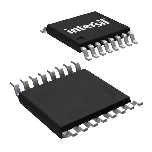
16 Ld SOIC
M16.3
10 +IN3
9 -IN3
8 OUT3
1
+-
4
+-
+IN2 5
-IN2 6
OUT2 7
NC 8
16 OUT4
15 -IN4
14 +IN4
13 V-
V+ 4
PACKAGE
13 -IN4
HA5104 (SOIC)
TOP VIEW
-IN1 2
PKG.
DWG. #
5 +IN2
14 OUT4
4
V+ 4
HA-5102 Dual, Comp. HA-5104 Quad, Comp.
Ordering Information
6 -IN2
HA-5104 (CERDIP)
TOP VIEW
These operational amplifiers are available in dual or quad
form with industry standard pinouts allowing for immediate
interchangeability with most other dual and quad operational
amplifiers.
TEMP. RANGE
PART NUMBER
(oC)
7 OUT2
+-
V- 4
OUT2 7
Refer to the /883 data sheet for military product.
8 V+
+
-
2
+
-
3
12 +IN3
11 -IN3
10 OUT3
9 NC
Features
•
•
•
•
•
Low Noise . . . . . . . . . . . . . . . . . . . . . . . . . . . . . 4.3nV/Hz
Bandwidth . . . . . . . . . . . . . . . . . . . . 8MHz (Compensated)
Slew Rate . . . . . . . . . . . . . . . . . . . . 3V/s (Compensated)
Low Offset Voltage . . . . . . . . . . . . . . . . . . . . . . . . . 0.5mV
Available in Duals or Quads
Applications
•
•
•
•
•
•
High Q, Active Filters
Audio Amplifiers
Instrumentation Amplifiers
Integrators
Signal Generators
For Further Design Ideas, See Application Note AN554
FN2925 Rev 9.00
October 26, 2004
Page 1 of 13
�HA-5102, HA-5104
Absolute Maximum Ratings
Thermal Information
Supply Voltage Between V+ and V- Terminals . . . . . . . . . . . . . 40V
Differential Input Voltage . . . . . . . . . . . . . . . . . . . . . . . . . . . . . . . 7V
Input Voltage . . . . . . . . . . . . . . . . . . . . . . . . . . . . . . . . . . VSUPPLY
Output Short Circuit Duration (Note 3). . . . . . . . . . . . . . . . Indefinite
Thermal Resistance (Typical, Note 2)
JA (oC/W)
JC (oC/W)
8 Lead CERDIP Package. . . . . . . . . . .
115
28
14 Lead CERDIP Package. . . . . . . . . .
75
20
SOIC Package . . . . . . . . . . . . . . . . . . .
100
N/A
Maximum Junction Temperature (Note 1, Hermetic Package) . .175oC
Maximum Junction Temperature (Plastic Package) . . . . . . . .150oC
Maximum Storage Temperature Range . . . . . . . . . -65oC to 150oC
Maximum Lead Temperature (Soldering 10s) . . . . . . . . . . . . 300oC
(SOIC - Lead Tips Only)
Operating Conditions
Temperature Range
HA-510X-2 . . . . . . . . . . . . . . . . . . . . . . . . . . . . . . -55oC to 125oC
HA-5104-9 . . . . . . . . . . . . . . . . . . . . . . . . . . . . . . . -40oC to 85oC
CAUTION: Stresses above those listed in “Absolute Maximum Ratings” may cause permanent damage to the device. This is a stress only rating and operation of the
device at these or any other conditions above those indicated in the operational sections of this specification is not implied.
NOTES:
1. Maximum power dissipation, including output load, must be designed to maintain the maximum junction temperature below 175oC for hermetic
packages, and below 150oC for plastic packages.
2. JA is measured with the component mounted on a low effective thermal conductivity test board in free air. See Tech Brief TB379 for details.
3. Any one amplifier may be shorted to ground indefinitely.
Electrical Specifications
VSUPPLY = 15V, Unless Otherwise Specified
HA-5102-2
HA-5104-2
HA-5104-9
TEMP.
(oC)
MIN
TYP
MAX
MIN
TYP
MAX
MIN
TYP
MAX
UNITS
25
-
0.5
2.0
-
0.5
2.5
-
0.5
2.5
mV
Full
-
-
2.5
-
-
3.0
-
-
3.0
mV
Offset Voltage Average Drift
Full
-
3
-
-
3
-
-
3
-
V/oC
Bias Current
25
-
130
200
-
130
200
-
130
200
nA
Full
-
-
325
-
-
325
-
-
500
nA
25
-
30
75
-
30
75
-
30
75
nA
Full
-
-
125
-
-
125
-
-
125
nA
Input Resistance
25
-
500
-
-
500
-
-
500
-
k
Common Mode Range
Full
12
-
-
12
-
-
12
-
-
V
25
100
250
-
100
250
-
80
250
-
kV/V
Full
100
-
-
100
-
-
80
-
-
kV/V
Common Mode Rejection Ratio (VCM = 5.0V)
Full
86
95
-
86
95
-
80
95
-
dB
Small Signal Bandwidth, (AV = 1)
25
-
8
-
-
8
-
-
8
-
MHz
Channel Separation (Note 4)
25
-
60
-
-
60
-
-
60
-
dB
(RL = 10k)
Full
12
13
-
12
13
-
12
13
-
V
(RL = 2k)
Full
10
12
-
10
12
-
10
12
-
V
Output Current, (VOUT = 5V)
Full
10
15
-
10
15
-
7
15
-
mA
Full Power Bandwidth (Note 5)
25
16
47
-
16
47
-
16
47
-
kHz
Output Resistance
25
-
110
-
-
110
-
-
110
-
Full
1
-
-
1
-
-
1
-
-
V/V
PARAMETER
INPUT CHARACTERISTICS
Offset Voltage
Offset Current
TRANSFER CHARACTERISTICS
Large Signal Voltage Gain,
(VOUT = 5V, RL = 2k
OUTPUT CHARACTERISTICS
Output Voltage Swing
STABILITY
Minimum Stable Closed Loop Gain
TRANSIENT RESPONSE (Note 6)
FN2925 Rev 9.00
October 26, 2004
Page 2 of 13
�HA-5102, HA-5104
Electrical Specifications
VSUPPLY = 15V, Unless Otherwise Specified (Continued)
HA-5102-2
HA-5104-2
HA-5104-9
TEMP.
(oC)
MIN
TYP
MAX
MIN
TYP
MAX
MIN
TYP
MAX
UNITS
Rise Time
25
-
108
200
-
108
200
-
108
200
ns
Overshoot
25
-
20
35
-
20
35
-
20
35
%
Slew Rate
25
1
3
-
1
3
-
1
3
-
V/s
Settling Time (Note 7)
25
-
4.5
-
-
4.5
-
-
4.5
-
s
f = 10Hz
25
-
9
25
-
9
25
-
9
25
nV/Hz
f = 1kHz
25
-
4.3
6.0
-
4.3
6.0
-
4.3
6.0
nV/Hz
f = 10Hz
25
-
5.1
15
-
5.1
15
-
5.1
15
pA/Hz
f = 1kHz
25
-
0.57
3
-
0.57
3
-
0.57
3
pA/Hz
f = DC to 30kHz
25
-
870
-
-
870
-
-
870
-
nVRMS
Supply Current (All Amps)
25
-
3.0
5.0
-
5.0
6.5
-
5.0
6.5
mA
Power Supply Rejection Ratio, (VS = 5V)
Full
86
100
-
86
100
-
80
100
-
dB
PARAMETER
NOISE CHARACTERISTICS (Note 8)
Input Noise Voltage
Input Noise Current
Broadband Noise Voltage
POWER SUPPLY CHARACTERISTICS
NOTES:
4. Channel separation value is referred to the input of the amplifier. Input test conditions are: f = 10kHz; VIN = 100mVPEAK; RS = 1k.
Slew Rate
5. Full power bandwidth is guaranteed by equation: Full power bandwidth = ----------------------------- .
2V PEAK
6. Refer to Test Circuits section of the data sheet.
7. Settling time is measured to 0.1% of final value for a 10V input step, AV = -1.
8. The limits for these parameters are guaranteed based on lab characterization, and reflect lot-to-lot variation.
FN2925 Rev 9.00
October 26, 2004
Page 3 of 13
�HA-5102, HA-5104
Test Circuits and Waveforms
2k
2k
-
IN
+
IN
OUT
+
-
50pF
1k
2k
50pF
OUTPUT
+5V
INPUT
200mV
0V
INPUT
-5V
+5V
OUTPUT
0V
0V
-5V
Vertical = 5V/Div., Horizontal = 5s/Div. (AV = -1)
Vertical = 40mV/Div., Horizontal = 50ns/Div. (AV = +1)
FIGURE 1. LARGE SIGNAL RESPONSE CIRCUIT
FIGURE 2. SMALL SIGNAL RESPONSE CIRCUIT
+15V
2N4416
5k
500 (NOTE 9)
TO
OSCILLOSCOPE
5k
2k
+15V
+
VOUT
-
VIN
-15V
200 (NOTE 9)
2k
50pF
2k
NOTES:
9. AV = -1.
10. Feedback and summing resistors should be 0.1% matched.
11. Clipping diodes are optional, HP5082-2810 recommended.
FIGURE 3. SETTLING TIME CIRCUIT
FN2925 Rev 9.00
October 26, 2004
Page 4 of 13
�HA-5102, HA-5104
Simplified Schematic
V+
OUTPUT
V+INPUT
-INPUT
Typical Performance Curves
10
VS = 15V, TA = 25oC
NOISE CURRENT (pA/Hz)
NOISE VOLTAGE (nV/Hz)
15
HIGH
10
TYPICAL
LOW
5
0
10
100
FREQUENCY (Hz)
FIGURE 4. INPUT NOISE VOLTAGE DENSITY
FN2925 Rev 9.00
October 26, 2004
1K
VS = 15V, TA = 25oC
5.0
1.0
0.5
0.1
10
100
1K
FREQUENCY (Hz)
FIGURE 5. INPUT NOISE CURRENT DENSITY
Page 5 of 13
�HA-5102, HA-5104
Typical Performance Curves
(Continued)
VS = 15V, TA = 25oC, 50V/Div., 1s/Div., AV = 1000V/V
Input Noise = 0.232VP-P
FIGURE 6. 0.1Hz TO 10Hz NOISE
VS = 15V, TA = 25oC, 500V/Div., 1s/Div., AV = 1000V/V
Total Output Noise = 2.075VP-P
FIGURE 7. 0.1Hz TO 1MHz NOISE
2.0
TA = 25oC
VS = 15V
OFFSET VOLTAGE (mV)
INPUT OFFSET VOLTAGE (mV)
2.0
1.5
1.0
0.5
0
-60
-40
-20
0
20
40
60
80
100
1.5
1.0
0.5
0
120
0
2
4
TEMPERATURE (oC)
90
INPUT BIAS CURRENT (nA)
INPUT OFFSET CURRENT (nA)
100
10
12
14
16
18
VS = 15V
80
70
60
50
40
30
20
10
0
20
40
60
80
TEMPERATURE (oC)
FIGURE 10. IIO vs TEMPERATURE
FN2925 Rev 9.00
October 26, 2004
8
FIGURE 9. VIO vs VS
FIGURE 8. VIO vs TEMPERATURE
4
2 VS = 15V
0
-2
-4
-6
-8
-10
-12
-14
-16
-18
-20
-22
-24
-26
-60
-40
-20
6
SUPPLY VOLTAGE (V)
100
120
0
-60
-40
-20
0
20
40
60
80
100
120
TEMPERATURE (oC)
FIGURE 11. IBIAS vs TEMPERATURE
Page 6 of 13
�HA-5102, HA-5104
Typical Performance Curves
5
VS = 15V, IOUT = 0
TOTAL SUPPLY CURRENT (mA)
TOTAL SUPPLY CURRENT (mA)
5
(Continued)
4
3
2
1
0
-60
-40
-20
0
20
40
60
80
100
4
3
2
1
0
120
TA = 25oC, IOUT = 0
0
2
4
TEMPERATURE (oC)
FIGURE 12. ICC vs TEMPERATURE (HA-5104)
3
2
1
-60
-40
-20
0
20
40
60
80
100
VO = 10V, VS = 15V
5.0
14
16
18
6K
8K 10K
125oC
25oC
-55oC
3.0
2.0
1K
120
2K
4K
LOAD RESISTANCE ()
FIGURE 14. AVOL vs TEMPERATURE
FIGURE 15. AVOL vs LOAD RESISTANCE
13
TA = 25oC, RL = 2k
TA = 25oC, RL = 2k
12
MAX OUTPUT SWING (V)
OPEN LOOP GAIN (kV/V)
12
4.0
TEMPERATURE (oC)
290
280
270
260
250
240
230
220
210
200
190
180
170
160
150
140
130
10
5.5
VS = 15V, VO = 10V, RL = 2k
4
0
8
FIGURE 13. ICC vs VS (HA-5102)
OPEN LOOP VOLTAGE GAIN (105V/V)
OPEN LOOP VOLTAGE GAIN (105V/V)
5
6
SUPPLY VOLTAGE (V)
11
10
9
8
7
6
5
4
3
2
1
0
2
4
6
8
10
12
SUPPLY VOLTAGE (V)
FIGURE 16. AVOL vs VS
FN2925 Rev 9.00
October 26, 2004
14
16
18
0
0
2
4
6
8
10
12
14
16
SUPPLY VOLTAGE (V)
FIGURE 17. VOUT vs VS
Page 7 of 13
18
�HA-5102, HA-5104
Typical Performance Curves
0
VS = 15V, TA = 25oC
40
-20
35
CMRR (dB)
VOUT = -15V
30
-40
-60
VOUT = +15V
25
20
-80
0
50
100
150
200
250
300
350
400
-100
1K
450
10K
TIME (SECONDS)
0
6
-20
0
-40
+PSRR
-PSRR
-80
10K
100K
-3
-12
125oC
PHASE
0
0
45
90
PHASE
135
100K
1M
10M
180
100M
FREQUENCY (Hz)
FIGURE 22. OPEN LOOP GAIN vs FREQUENCY
FN2925 Rev 9.00
October 26, 2004
OVERSHOOT (%)
20
PHASE SHIFT (DEGREES)
VOLTAGE GAIN (dB)
40
10K
100K
1M
10M
-225
40M
VS = 15V, TA = 25oC, RL = 2k
50
GAIN
1K
-135
-55oC
PHASE
60
80
100
-45
FIGURE 21. UNITY GAIN FREQUENCY RESPONSE
VS = 15V, TA = 25oC,
RL = 2k , CL = 50pF
60
45
FREQUENCY (Hz)
FIGURE 20. PSRR vs FREQUENCY
100
135
0
FREQUENCY (Hz)
120
-55oC
GAIN
125oC
GAIN
-6
-24
10K
1M
225
VS = 15V, RL = 2k, CL = 50pF
-18
-100
1K
1M
FIGURE 19. CMRR vs FREQUENCY
VOLTAGE GAIN (dB)
POWER SUPPLY REJECTION (dB)
FIGURE 18. OUTPUT SHORT CIRCUIT CURRENT vs TIME
-60
100K
FREQUENCY (Hz)
PHASE SHIFT (DEGREES)
OUTPUT CURRENT (mA)
45
(Continued)
40
30
20
10
0
10
100
1K
LOAD CAPACITANCE (pF)
FIGURE 23. SMALL SIGNAL OVERSHOOT vs CLOAD
Page 8 of 13
10K
�HA-5102, HA-5104
Typical Performance Curves
1.1
RL = 2k, CL = 50pF, VS = 15V
RL = 2k, CL = 50pF, VS = 15V
1.0
RISE TIME (NORMALIZED)
SLEW RATE (NORMALIZED)
1.1
(Continued)
0.9
0.8
0.7
0.6
-60
-40
-20
0
20
40
60
80
100
1.0
0.9
0.8
0.7
0.6
-60
120
-40
-20
0
20
40
60
80
100
120
TEMPERATURE (oC)
TEMPERATURE (oC)
FIGURE 25. RISE TIME vs TEMPERATURE
FIGURE 24. SLEW RATE vs TEMPERATURE
PASSIVATION:
Die Characteristics
Type: Nitride (Si3N4) over Silox (SiO2, 5% Phos.)
Silox Thickness: 12kÅ 2kÅ
Nitride Thickness: 3.5kÅ 1.5kÅ
DIE DIMENSIONS:
98.4 mils x 67.3 mils x 19 mils
2500m x 1710m x 483m
SUBSTRATE POTENTIAL (POWERED UP):
METALLIZATION:
Unbiased
Type: Al, 1% Cu
Thickness: 16kÅ 2kÅ
TRANSISTOR COUNT:
93
PROCESS:
Bipolar Dielectric Isolation
Metallization Mask Layout
HA-5102
FN2925 Rev 9.00
October 26, 2004
V-
+IN1
-IN1
OUT1
+IN2
-IN2
OUT2
V+
Page 9 of 13
�HA-5102, HA-5104
SUBSTRATE POTENTIAL (POWERED UP):
Die Characteristics
Unbiased
DIE DIMENSIONS:
TRANSISTOR COUNT:
95 mils x 99 mils x 19 mils
2420m x 2530m x 483m
175
METALLIZATION:
PROCESS:
Type: Al, 1% Cu
Thickness: 16kÅ 2kÅ
Bipolar Dielectric Isolation
PASSIVATION:
Type: Nitride (Si3N4) over Silox (SiO2, 5% Phos.)
Silox Thickness: 12kÅ 2kÅ
Nitride Thickness: 3.5kÅ 1.5kÅ
Metallization Mask Layout
HA-5104
+IN2
V+
+IN1
-IN1
-IN2
OUT2
OUT1
OUT3
OUT4
-IN3
-IN4
+IN3
FN2925 Rev 9.00
October 26, 2004
V-
+IN4
Page 10 of 13
�HA-5102, HA-5104
Ceramic Dual-In-Line Frit Seal Packages (CERDIP)
F8.3A MIL-STD-1835 GDIP1-T8 (D-4, CONFIGURATION A)
LEAD FINISH
c1
8 LEAD CERAMIC DUAL-IN-LINE FRIT SEAL PACKAGE
-D-
-A-
BASE
METAL
(c)
E
M
-Bbbb S
C A-B S
Q
-C-
SEATING
PLANE
S1
b2
b
ccc M
C A-B S
D S
eA/2
NOTES
-
0.200
-
5.08
-
0.014
0.026
0.36
0.66
2
b1
0.014
0.023
0.36
0.58
3
b2
0.045
0.065
1.14
1.65
-
b3
0.023
0.045
0.58
1.14
4
c
0.008
0.018
0.20
0.46
2
c1
0.008
0.015
0.20
0.38
3
D
-
0.405
-
10.29
5
E
0.220
0.310
5.59
7.87
5
eA
e
MAX
b
A A
MIN
A
A
L
MILLIMETERS
MAX
M
(b)
D
BASE
PLANE
MIN
b1
SECTION A-A
D S
INCHES
SYMBOL
c
aaa M C A - B S D S
NOTES:
1. Index area: A notch or a pin one identification mark shall be located adjacent to pin one and shall be located within the shaded
area shown. The manufacturer’s identification shall not be used
as a pin one identification mark.
e
0.100 BSC
2.54 BSC
-
eA
0.300 BSC
7.62 BSC
-
eA/2
0.150 BSC
3.81 BSC
-
L
0.125
0.200
3.18
5.08
-
Q
0.015
0.060
0.38
1.52
6
S1
0.005
-
0.13
-
7
105o
90o
105o
-
2. The maximum limits of lead dimensions b and c or M shall be
measured at the centroid of the finished lead surfaces, when
solder dip or tin plate lead finish is applied.
90o
aaa
-
0.015
-
0.38
-
3. Dimensions b1 and c1 apply to lead base metal only. Dimension
M applies to lead plating and finish thickness.
bbb
-
0.030
-
0.76
-
ccc
-
0.010
-
0.25
-
M
-
0.0015
-
0.038
2, 3
4. Corner leads (1, N, N/2, and N/2+1) may be configured with a
partial lead paddle. For this configuration dimension b3 replaces
dimension b2.
5. This dimension allows for off-center lid, meniscus, and glass
overrun.
N
8
8
8
Rev. 0 4/94
6. Dimension Q shall be measured from the seating plane to the
base plane.
7. Measure dimension S1 at all four corners.
8. N is the maximum number of terminal positions.
9. Dimensioning and tolerancing per ANSI Y14.5M - 1982.
10. Controlling dimension: INCH
FN2925 Rev 9.00
October 26, 2004
Page 11 of 13
�HA-5102, HA-5104
Ceramic Dual-In-Line Frit Seal Packages (CERDIP)
F14.3 MIL-STD-1835 GDIP1-T14 (D-1, CONFIGURATION A)
14 LEAD CERAMIC DUAL-IN-LINE FRIT SEAL PACKAGE
LEAD FINISH
c1
-D-
-A-
BASE
METAL
(c)
E
M
-Bbbb S
C A-B S
Q
-C-
SEATING
PLANE
S1
b2
b
ccc M
C A-B S
D S
eA/2
NOTES
-
0.200
-
5.08
-
0.014
0.026
0.36
0.66
2
b1
0.014
0.023
0.36
0.58
3
b2
0.045
0.065
1.14
1.65
-
b3
0.023
0.045
0.58
1.14
4
c
0.008
0.018
0.20
0.46
2
c1
0.008
0.015
0.20
0.38
3
D
-
0.785
-
19.94
5
E
0.220
0.310
5.59
7.87
5
eA
e
MAX
b
A A
MIN
A
A
L
MILLIMETERS
MAX
M
(b)
D
BASE
PLANE
MIN
b1
SECTION A-A
D S
INCHES
SYMBOL
c
aaa M C A - B S D S
NOTES:
1. Index area: A notch or a pin one identification mark shall be located adjacent to pin one and shall be located within the shaded
area shown. The manufacturer’s identification shall not be used
as a pin one identification mark.
e
0.100 BSC
2.54 BSC
-
eA
0.300 BSC
7.62 BSC
-
eA/2
0.150 BSC
3.81 BSC
-
L
0.125
0.200
3.18
5.08
-
Q
0.015
0.060
0.38
1.52
6
S1
0.005
-
0.13
-
7
105o
90o
105o
-
2. The maximum limits of lead dimensions b and c or M shall be
measured at the centroid of the finished lead surfaces, when
solder dip or tin plate lead finish is applied.
90o
aaa
-
0.015
-
0.38
-
3. Dimensions b1 and c1 apply to lead base metal only. Dimension
M applies to lead plating and finish thickness.
bbb
-
0.030
-
0.76
-
ccc
-
0.010
-
0.25
-
M
-
0.0015
-
0.038
2, 3
4. Corner leads (1, N, N/2, and N/2+1) may be configured with a
partial lead paddle. For this configuration dimension b3 replaces
dimension b2.
5. This dimension allows for off-center lid, meniscus, and glass
overrun.
N
14
14
8
Rev. 0 4/94
6. Dimension Q shall be measured from the seating plane to the
base plane.
7. Measure dimension S1 at all four corners.
8. N is the maximum number of terminal positions.
9. Dimensioning and tolerancing per ANSI Y14.5M - 1982.
10. Controlling dimension: INCH.
FN2925 Rev 9.00
October 26, 2004
Page 12 of 13
�HA-5102, HA-5104
Small Outline Plastic Packages (SOIC)
M16.3 (JEDEC MS-013-AA ISSUE C)
N
16 LEAD WIDE BODY SMALL OUTLINE PLASTIC PACKAGE
INDEX
AREA
0.25(0.010) M
H
B M
INCHES
E
-B-
1
2
3
L
SEATING PLANE
-A-
h x 45o
A
D
-C-
e
A1
B
0.25(0.010) M
C
0.10(0.004)
C A M
SYMBOL
MIN
MAX
MIN
MAX
NOTES
A
0.0926
0.1043
2.35
2.65
-
A1
0.0040
0.0118
0.10
0.30
-
B
0.013
0.0200
0.33
0.51
9
C
0.0091
0.0125
0.23
0.32
-
D
0.3977
0.4133
10.10
10.50
3
E
0.2914
0.2992
7.40
7.60
4
e
µ
B S
0.050 BSC
1.27 BSC
-
H
0.394
0.419
10.00
10.65
-
h
0.010
0.029
0.25
0.75
5
L
0.016
0.050
0.40
1.27
6
N
NOTES:
MILLIMETERS
16
0o
16
8o
0o
1. Symbols are defined in the “MO Series Symbol List” in Section 2.2 of
Publication Number 95.
7
8o
Rev. 0 12/93
2. Dimensioning and tolerancing per ANSI Y14.5M-1982.
3. Dimension “D” does not include mold flash, protrusions or gate burrs.
Mold flash, protrusion and gate burrs shall not exceed 0.15mm (0.006
inch) per side.
4. Dimension “E” does not include interlead flash or protrusions. Interlead
flash and protrusions shall not exceed 0.25mm (0.010 inch) per side.
5. The chamfer on the body is optional. If it is not present, a visual index
feature must be located within the crosshatched area.
6. “L” is the length of terminal for soldering to a substrate.
7. “N” is the number of terminal positions.
8. Terminal numbers are shown for reference only.
9. The lead width “B”, as measured 0.36mm (0.014 inch) or greater above
the seating plane, shall not exceed a maximum value of 0.61mm (0.024
inch)
10. Controlling dimension: MILLIMETER. Converted inch dimensions are
not necessarily exact.
© Copyright Intersil Americas LLC 2003-2004. All Rights Reserved.
All trademarks and registered trademarks are the property of their respective owners.
For additional products, see www.intersil.com/en/products.html
Intersil products are manufactured, assembled and tested utilizing ISO9001 quality systems as noted
in the quality certifications found at www.intersil.com/en/support/qualandreliability.html
Intersil products are sold by description only. Intersil may modify the circuit design and/or specifications of products at any time without notice, provided that such
modification does not, in Intersil's sole judgment, affect the form, fit or function of the product. Accordingly, the reader is cautioned to verify that datasheets are
current before placing orders. Information furnished by Intersil is believed to be accurate and reliable. However, no responsibility is assumed by Intersil or its
subsidiaries for its use; nor for any infringements of patents or other rights of third parties which may result from its use. No license is granted by implication or
otherwise under any patent or patent rights of Intersil or its subsidiaries.
For information regarding Intersil Corporation and its products, see www.intersil.com
FN2925 Rev 9.00
October 26, 2004
Page 13 of 13
�