HAT2172N
Silicon N Channel Power MOS FET Power Switching
REJ03G1683-0100 Rev.1.00 May 28, 2008
Features
• • • • • High speed switching Capable of 7 V gate drive Low drive current High density mounting Low on-resistance RDS(on) = 6.1 mΩ typ. (at VGS = 10 V)
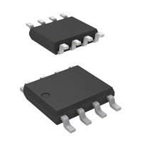
Outline
RENESAS Package code: PTSP0008DC-A (Package name: LFPAK-i)
1(S) 2(S) 3(S) 4(G) 5678 DDDD
2X XX
8(D) 7(D) 6(D) 5(D)
4 G
1, 2, 3 Source 4 Gate 5, 6, 7, 8 Drain
SSS 123
Absolute Maximum Ratings
(Ta = 25°C)
Item Drain to source voltage Gate to source voltage Drain current Drain peak current Body-drain diode reverse drain current Avalanche current Avalanche energy Channel dissipation Channel to case thermal resistance Channel temperature Storage temperature Notes: 1. PW ≤ 10 µs, duty cycle ≤ 1% 2. Value at Tch = 25°C, Rg ≥ 50 Ω 3. Tc = 25°C Symbol VDSS VGSS ID ID(pulse) Note1 IDR IAP Note 2 EAR Note 2 Pch Note3 θch-C Tch Tstg Ratings 40 ±20 30 120 30 20 20 20 6.25 150 –55 to +150 Unit V V A A A A mJ W °C/W °C °C
REJ03G1683-0100 Rev.1.00 May 28, 2008 Page 1 of 7
�HAT2172N
Electrical Characteristics
(Ta = 25°C)
Item Drain to source breakdown voltage Gate to source breakdown voltage Gate to source leak current Zero gate voltage drain current Gate to source cutoff voltage Static drain to source on state resistance Forward transfer admittance Input capacitance Output capacitance Reverse transfer capacitance Gate resistance Total gate charge Gate to source charge Gate to drain charge Turn-on delay time Rise time Turn-off delay time Fall time Body–drain diode forward voltage Body–drain diode reverse recovery time Notes: 4. Pulse test Symbol V(BR)DSS V(BR)GSS IGSS IDSS VGS(off) RDS(on) RDS(on) |yfs| Ciss Coss Crss Rg Qg Qgs Qgd td(on) tr td(off) tf VDF trr Min 40 ±20 — — 1.5 — — 27 — — — — — — — — — — — — — Typ — — — — — 6.1 6.9 45 2420 480 150 0.5 32 9 4.0 12 20 38 4.5 0.84 32 Max — — ±10 1 3.0 7.8 9.5 — — — — — — — — — — — — 1.10 — Unit V V µA µA V mΩ mΩ S pF pF pF Ω nC nC nC ns ns ns ns V ns Test Conditions ID = 10 mA, VGS = 0 IG = ±100 µA, VDS = 0 VGS = ±16 V, VDS = 0 VDS = 40 V, VGS = 0 VDS = 10 V, ID = 10mA ID = 15 A, VGS = 10 V Note4 ID = 15 A, VGS = 7 V Note4 ID = 15 A, VDS = 10 V Note4 VDS = 10 V,VGS = 0, f = 1 MHz
VDD = 10 V, VGS = 10 V, ID = 30 A VGS = 10 V, ID = 15 A, VDD ≅ 10 V, RL = 0.67 Ω, Rg = 4.7 Ω IF = 30 A, VGS = 0 Note4 IF = 30 A, VGS = 0 diF/ dt = 100 A/ µs
REJ03G1683-0100 Rev.1.00 May 28, 2008 Page 2 of 7
�HAT2172N
Main Characteristics
Power vs. Temperature Derating
40 500 100
1m
10
10
Maximum Safe Operation Area
Channel Dissipation Pch (W)
Drain Current ID (A)
30
PW
10
DC
Op
=1
c=
era
tio
s 0m s
°C
0µ
µs
s
20
nT
1 Operation in this area is 0.1 limited by RDS(on) Ta = 25°C 1 shot Pulse 0.3 1 3
25
10
0
50
100
150
200
0.01 0.1
10
30
100
Case Temperature Tc (°C)
Drain to Source Voltage VDS (V)
Typical Output Characteristics
50 10 V Pulse Test 4.0 V 4.4 V 3.8 V 50
Typical Transfer Characteristics
VDS = 10 V Pulse Test
Drain Current ID (A)
30 3.6 V 20 3.4 V 10
Drain Current ID (A)
40
40
30 Tc = 75°C
20
10
VGS = 3.0 V
0 2 4 6 8 10 0 2
25°C –25°C 4 6 8 10
Drain to Source Voltage VDS (V) Drain to Source Saturation Voltage vs. Gate to Source Voltage
Drain to Source Voltage VDS(on) (mV) Drain to Source On State Resistance RDS(on) (mΩ)
200 Pulse Test 150 ID = 20 A 100
Gate to Source Voltage VGS (V) Static Drain to Source on State Resistance vs. Drain Current
100 50
20 10 5 VGS = 7 V 10 V
10 A 50 5A
2 1 1 0.3 10 3 Pulse Test 100 30 1000
0
4
8
12
16
20
Gate to Source Voltage VGS (V)
Drain Current
ID (A)
REJ03G1683-0100 Rev.1.00 May 28, 2008 Page 3 of 7
�HAT2172N
Static Drain to Source on State Resistance vs. Temperature Forward Transfer Admittance vs. Drain Current
Forward Transfer Admittance |yfs| (S)
Drain to Source On State Resistance RDS(on) (mΩ)
20
100 30 10 3 1 0.3 0.1 0.1 Tc = –25°C 25°C
Pulse Test
15 ID = 20 A 10 VGS = 7 V 5 10 V 0 –25 5 A, 10 A, 20 A 5 A, 10 A
75°C
VDS = 10 V Pulse Test 0.3 1 3 10 30 100
0
25
50
75
100 125 150
Case Temperature Tc (°C)
Drain Current ID (A)
Body-Drain Diode Reverse Recovery Time
100 10000 3000 1000
Typical Capacitance vs. Drain to Source Voltage
Reverse Recovery Time trr (ns)
Ciss
50
Capacitance C (pF)
Coss 300 Crss 100 30 V = 0 GS f = 1 MHz 10 0 5 10
20 di/dt = 100 A/µs VGS = 0, Ta = 25°C 10 0.1 0.3 1 3 10 30 100
15
20
25
30
Reverse Drain Current IDR (A)
Drain to Source Voltage VDS (V)
Dynamic Input Characteristics
Switching Characteristics
20
Drain to Source Voltage VDS (V)
50
Gate to Source Voltage VGS (V)
ID = 30 A
1000 300 100 td(off) 30 td(on) 10 tf 3 1 0.1 VGS = 10 V, VDS = 10 V Rg = 4.7 Ω, duty ≤ 1 % 0.3 1 3 10 30 100 tr
VGS 30 VDS VDD = 25 V 10 V 5V 12
20
8
10
VDD = 25 V 10 V 5V 8 16 24 32
4 0 40
0
Gate Charge Qg (nc)
Switching Time t (ns)
40
16
Drain Current ID (A)
REJ03G1683-0100 Rev.1.00 May 28, 2008 Page 4 of 7
�HAT2172N
Reverse Drain Current vs. Source to Drain Voltage
50
Maximum Avalanche Energy vs. Channel Temperature Derating
Repetitive Avalanche Energy EAR (mJ)
50 IAP = 20 A VDD = 15 V duty < 0.1 % Rg ≥ 50 Ω
Reverse Drain Current IDR (A)
10 V 40 5V VGS = 0, –5 V
40
30
30
20
20
10 Pulse Test 0 0.4 0.8 1.2 1.6 2.0
10 0 25
50
75
100
125
150
Source to Drain Voltage VSD (V)
Channel Temperature Tch (°C)
Normalized Transient Thermal Impedance vs. Pulse Width
Normalized Transient Thermal Impedance γs (t)
3 Tc = 25°C 1 D=1 0.5 0.3
0.2
0.1
0.1
0.05
θch - c(t) = γs (t) • θch - c θch - c = 6.25°C/ W, Tc = 25°C PDM D= PW T 1m 10 m 100 m 1 10 PW T
0.03
0.02 1 0.0
0.01 10 µ
1s
t ho
pu
lse
100 µ
Pulse Width PW (s)
REJ03G1683-0100 Rev.1.00 May 28, 2008 Page 5 of 7
�HAT2172N
Avalanche Test Circuit
VDS Monitor L EAR = IAP Monitor Rg Vin 15 V D. U. T VDD V(BR)DSS IAP VDS ID
Avalanche Waveform
1 L • IAP2 • 2 VDSS VDSS - VDD
50 Ω
0
VDD
Switching Time Test Circuit Vin Monitor Rg D.U.T. RL VDS = 10 V Vin Vout Vin 10 V Vout Monitor
Switching Time Waveform 90% 10% 10% 90% td(on) tr 90% td(off) tf 10%
REJ03G1683-0100 Rev.1.00 May 28, 2008 Page 6 of 7
�HAT2172N
Package Dimensions
Package Name LFPAK-i JEITA Package Code RENESAS Code PTSP0008DC-A Previous Code LFPAK-iV MASS[Typ.] 0.080g
4.9 5.3Max 8 5
0.25 – 0.03
+ 0.05
3.2
0.60 – 0.30
+ 0.25
1 3.3
4 0.20 – 0.03
+ 0.05
6.1 – 0.3
3.95
+ 0.1
0° – 8°
1.1Max
0.07 – 0.04
+ 0.03
0.75Max 1.27 0.10 0.4 ± 0.06 0.25 M ( Ni/Pd/Au plating )
Ordering Information
Part No. HAT2172N-EL-E Quantity 2500 pcs Taping Shipping Container
REJ03G1683-0100 Rev.1.00 May 28, 2008 Page 7 of 7
1.3Max
�Sales Strategic Planning Div.
Nippon Bldg., 2-6-2, Ohte-machi, Chiyoda-ku, Tokyo 100-0004, Japan
Notes: 1. This document is provided for reference purposes only so that Renesas customers may select the appropriate Renesas products for their use. Renesas neither makes warranties or representations with respect to the accuracy or completeness of the information contained in this document nor grants any license to any intellectual property rights or any other rights of Renesas or any third party with respect to the information in this document. 2. Renesas shall have no liability for damages or infringement of any intellectual property or other rights arising out of the use of any information in this document, including, but not limited to, product data, diagrams, charts, programs, algorithms, and application circuit examples. 3. You should not use the products or the technology described in this document for the purpose of military applications such as the development of weapons of mass destruction or for the purpose of any other military use. When exporting the products or technology described herein, you should follow the applicable export control laws and regulations, and procedures required by such laws and regulations. 4. All information included in this document such as product data, diagrams, charts, programs, algorithms, and application circuit examples, is current as of the date this document is issued. Such information, however, is subject to change without any prior notice. Before purchasing or using any Renesas products listed in this document, please confirm the latest product information with a Renesas sales office. Also, please pay regular and careful attention to additional and different information to be disclosed by Renesas such as that disclosed through our website. (http://www.renesas.com ) 5. Renesas has used reasonable care in compiling the information included in this document, but Renesas assumes no liability whatsoever for any damages incurred as a result of errors or omissions in the information included in this document. 6. When using or otherwise relying on the information in this document, you should evaluate the information in light of the total system before deciding about the applicability of such information to the intended application. Renesas makes no representations, warranties or guaranties regarding the suitability of its products for any particular application and specifically disclaims any liability arising out of the application and use of the information in this document or Renesas products. 7. With the exception of products specified by Renesas as suitable for automobile applications, Renesas products are not designed, manufactured or tested for applications or otherwise in systems the failure or malfunction of which may cause a direct threat to human life or create a risk of human injury or which require especially high quality and reliability such as safety systems, or equipment or systems for transportation and traffic, healthcare, combustion control, aerospace and aeronautics, nuclear power, or undersea communication transmission. If you are considering the use of our products for such purposes, please contact a Renesas sales office beforehand. Renesas shall have no liability for damages arising out of the uses set forth above. 8. Notwithstanding the preceding paragraph, you should not use Renesas products for the purposes listed below: (1) artificial life support devices or systems (2) surgical implantations (3) healthcare intervention (e.g., excision, administration of medication, etc.) (4) any other purposes that pose a direct threat to human life Renesas shall have no liability for damages arising out of the uses set forth in the above and purchasers who elect to use Renesas products in any of the foregoing applications shall indemnify and hold harmless Renesas Technology Corp., its affiliated companies and their officers, directors, and employees against any and all damages arising out of such applications. 9. You should use the products described herein within the range specified by Renesas, especially with respect to the maximum rating, operating supply voltage range, movement power voltage range, heat radiation characteristics, installation and other product characteristics. Renesas shall have no liability for malfunctions or damages arising out of the use of Renesas products beyond such specified ranges. 10. Although Renesas endeavors to improve the quality and reliability of its products, IC products have specific characteristics such as the occurrence of failure at a certain rate and malfunctions under certain use conditions. Please be sure to implement safety measures to guard against the possibility of physical injury, and injury or damage caused by fire in the event of the failure of a Renesas product, such as safety design for hardware and software including but not limited to redundancy, fire control and malfunction prevention, appropriate treatment for aging degradation or any other applicable measures. Among others, since the evaluation of microcomputer software alone is very difficult, please evaluate the safety of the final products or system manufactured by you. 11. In case Renesas products listed in this document are detached from the products to which the Renesas products are attached or affixed, the risk of accident such as swallowing by infants and small children is very high. You should implement safety measures so that Renesas products may not be easily detached from your products. Renesas shall have no liability for damages arising out of such detachment. 12. This document may not be reproduced or duplicated, in any form, in whole or in part, without prior written approval from Renesas. 13. Please contact a Renesas sales office if you have any questions regarding the information contained in this document, Renesas semiconductor products, or if you have any other inquiries.
RENESAS SALES OFFICES
Refer to "http://www.renesas.com/en/network" for the latest and detailed information. Renesas Technology America, Inc. 450 Holger Way, San Jose, CA 95134-1368, U.S.A Tel: (408) 382-7500, Fax: (408) 382-7501 Renesas Technology Europe Limited Dukes Meadow, Millboard Road, Bourne End, Buckinghamshire, SL8 5FH, U.K. Tel: (1628) 585-100, Fax: (1628) 585-900 Renesas Technology (Shanghai) Co., Ltd. Unit 204, 205, AZIACenter, No.1233 Lujiazui Ring Rd, Pudong District, Shanghai, China 200120 Tel: (21) 5877-1818, Fax: (21) 6887-7858/7898 Renesas Technology Hong Kong Ltd. 7th Floor, North Tower, World Finance Centre, Harbour City, Canton Road, Tsimshatsui, Kowloon, Hong Kong Tel: 2265-6688, Fax: 2377-3473 Renesas Technology Taiwan Co., Ltd. 10th Floor, No.99, Fushing North Road, Taipei, Taiwan Tel: (2) 2715-2888, Fax: (2) 3518-3399 Renesas Technology Singapore Pte. Ltd. 1 Harbour Front Avenue, #06-10, Keppel Bay Tower, Singapore 098632 Tel: 6213-0200, Fax: 6278-8001 Renesas Technology Korea Co., Ltd. Kukje Center Bldg. 18th Fl., 191, 2-ka, Hangang-ro, Yongsan-ku, Seoul 140-702, Korea Tel: (2) 796-3115, Fax: (2) 796-2145
http://www.renesas.com
Renesas Technology Malaysia Sdn. Bhd Unit 906, Block B, Menara Amcorp, Amcorp Trade Centre, No.18, Jln Persiaran Barat, 46050 Petaling Jaya, Selangor Darul Ehsan, Malaysia Tel: 7955-9390, Fax: 7955-9510
© 2008. Renesas Technology Corp., All rights reserved. Printed in Japan.
Colophon .7.2
�


 工商网监
湘ICP备2023018690号
工商网监
湘ICP备2023018690号
