DATASHEET
HIP2100
FN4022
Rev.16.00
Aug 8, 2019
100V/2A Peak, Low Cost, High Frequency Half Bridge Driver
The HIP2100 is a high frequency, 100V Half Bridge
N-Channel power MOSFET driver IC. The low-side and
high-side gate drivers are independently controlled and
matched to 8ns. This gives the user maximum flexibility in
dead-time selection and driver protocol. Undervoltage
protection on both the low-side and high-side supplies force
the outputs low. An on-chip diode eliminates the discrete
diode required with other driver ICs. A new level-shifter
topology yields the low-power benefits of pulsed operation
with the safety of DC operation. Unlike some competitors,
the high-side output returns to its correct state after a
momentary undervoltage of the high-side supply.
Features
Applications
• Drives 1000pF Load with Rise and Fall Times Typ 10ns
• Telecom Half Bridge Power Supplies
• Avionics DC/DC Converters
• Two-Switch Forward Converters
• Drives N-Channel MOSFET Half Bridge
• SOIC, EPSOIC, and QFN Package Options
• SOIC and EPSOIC Packages Compliant with 100V
Conductor Spacing Guidelines of IPC-2221
• Pb-Free (RoHS Compliant)
• Bootstrap Supply Max Voltage to 114VDC
• On-Chip 1Ω Bootstrap Diode
• Fast Propagation Times for Multi-MHz Circuits
• CMOS Input Thresholds for Improved Noise Immunity
• Independent Inputs for Non-Half Bridge Topologies
• No Start-Up Problems
• Active Clamp Forward Converters
• Outputs Unaffected by Supply Glitches, HS Ringing Below
Ground, or HS Slewing at High dv/dt
Related Literature
• Low Power Consumption
For a full list of related documents, visit our website:
• HIP2100 device page
• Wide Supply Range
• Supply Undervoltage Protection
• 3Ω Driver Output Resistance
• QFN Package:
- Compliant to JEDEC PUB95 MO-220
QFN - Quad Flat No Leads - Package Outline
- Near Chip Scale Package Footprint, which Improves
PCB Efficiency and has a Thinner Profile
FN4022 Rev.16.00
Aug 8, 2019
Page 1 of 14
�HIP2100
Ordering Information
PART NUMBER
(Notes 2, 3)
PART
MARKING
TEMP. RANGE
(°C)
TAPE AND REEL
(Units) (Note 1)
PACKAGE
(RoHS Compliant)
PKG.
DWG. #
HIP2100IBZ
2100 IBZ
-40 to +125
-
8 Ld SOIC
M8.15
HIP2100IBZT
2100 IBZ
-40 to +125
2.5k
8 Ld SOIC
M8.15
HIP2100EIBZ
2100 EIBZ
-40 to +125
-
8 Ld EPSOIC
M8.15C
HIP2100EIBZT
2100 EIBZ
-40 to +125
2.5k
8 Ld EPSOIC
M8.15C
HIP2100IRZ
HIP 2100IRZ
-40 to +125
-
16 Ld 5x5 QFN
L16.5x5
HIP2100IRZT
HIP 2100IRZ
-40 to +125
6k
16 Ld 5x5 QFN
L16.5x5
HIP2100EVAL2
Evaluation Board
NOTES:
1. See TB347 for details about reel specifications.
2. These Pb-free plastic packaged products employ special Pb-free material sets, molding compounds/die attach materials, and 100% matte tin
plate plus anneal (e3 termination finish, which is RoHS compliant and compatible with both SnPb and Pb-free soldering operations). Pb-free
products are MSL classified at Pb-free peak reflow temperatures that meet or exceed the Pb-free requirements of IPC/JEDEC J-STD-020.
3. For Moisture Sensitivity Level (MSL), see the HIP2100 device page. For more information about MSL, see TB363.
Pinouts
(16 LD QFN)
TOP VIEW
LO
7
VSS
HO
3
6
LI
HS
4
5
HI
EPAD
NC
8
2
LO
1
HB
VDD
VDD
NC
(8 LD SOIC, EPSOIC)
TOP VIEW
16
15
14
13
NC 1
12 NC
HB 2
11 VSS
EPAD
9
5
6
7
8
NC
NC 4
HI
10 LI
HS
HO 3
NC
EPAD = Exposed PAD.
NC
Pin Descriptions
SYMBOL
DESCRIPTION
VDD
Positive Supply to lower gate drivers. De-couple this pin to VSS. Bootstrap diode connected to HB.
HB
High-Side Bootstrap supply. External bootstrap capacitor is required. Connect positive side of bootstrap capacitor to this pin.
Bootstrap diode is on-chip.
HO
High-Side Output. Connect to gate of High-Side power MOSFET.
HS
High-Side Source connection. Connect to source of High-Side power MOSFET. Connect negative side of bootstrap capacitor to
this pin.
HI
High-Side input.
LI
Low-Side input.
VSS
Chip negative supply, generally will be ground.
LO
Low-Side Output. Connect to gate of Low-Side power MOSFET.
EPAD
Exposed Pad. Connect to ground or float. The EPAD is electrically isolated from all other pins.
FN4022 Rev.16.00
Aug 8, 2019
Page 2 of 14
�HIP2100
Application Block Diagram
+12V
+100V
SECONDARY
CIRCUIT
VDD
HB
DRIVE
HI
PWM
CONTROLLER
LI
CONTROL
HI
HO
HS
DRIVE
LO
LO
REFERENCE
AND
ISOLATION
HIP2100
VSS
Functional Block Diagram
HB
VDD
UNDER
VOLTAGE
HO
LEVEL SHIFT
DRIVER
HS
HI
UNDER
VOLTAGE
LO
DRIVER
LI
VSS
EPAD (EPSOIC and QFN PACKAGES ONLY)
*EPAD = Exposed Pad. The EPAD is electrically isolated from all other pins. For best
thermal performance connect the EPAD to the PCB power ground plane.
FN4022 Rev.16.00
Aug 8, 2019
Page 3 of 14
�HIP2100
+48V
+12V
PWM
HIP2100
SECONDARY
CIRCUIT
ISOLATION
FIGURE 1. TWO-SWITCH FORWARD CONVERTER
+48V
SECONDARY
CIRCUIT
+12V
PWM
HIP2100
ISOLATION
FIGURE 2. FORWARD CONVERTER WITH AN ACTIVE CLAMP
FN4022 Rev.16.00
Aug 8, 2019
Page 4 of 14
�HIP2100
Absolute Maximum Ratings
Thermal Information
Supply Voltage, VDD, VHB-VHS (Notes 4, 5) . . . . . . . . -0.3V to 18V
LI and HI Voltages (Note 5) . . . . . . . . . . . . . . . . -0.3V to VDD +0.3V
Voltage on LO (Note 4) . . . . . . . . . . . . . . . . . . . -0.3V to VDD +0.3V
Voltage on HO (Note 4) . . . . . . . . . . . . . . . VHS -0.3V to VHB +0.3V
Voltage on HS (Continuous) (Note 4) . . . . . . . . . . . . . . -1V to 110V
Voltage on HB (Note 4) . . . . . . . . . . . . . . . . . . . . . . . . . . . . . +118V
Average Current in VDD to HB diode . . . . . . . . . . . . . . . . . . . 100mA
ESD Classification . . . . . . . . . . . . . . . . . . . . . . . . . . . Class 1 (1kV)
Thermal Resistance (Typical)
Maximum Recommended Operating Conditions
JA (°C/W)
JC (°C/W)
95
50
SOIC (Note 6) . . . . . . . . . . . . . . . . . . .
EPSOIC (Note 7) . . . . . . . . . . . . . . . . .
40
3.0
QFN (Note 7) . . . . . . . . . . . . . . . . . . . .
37
6.5
Max Power Dissipation at +25°C in Free Air (SOIC, Note 6) . . . . 1.3W
Max Power Dissipation at +25°C in Free Air (EPSOIC, Note 7). . 3.1W
Max Power Dissipation at +25°C in Free Air (QFN, Note 7) . . . . . 3.3W
Storage Temperature Range . . . . . . . . . . . . . . . . . .-65°C to +150°C
Junction Temperature Range. . . . . . . . . . . . . . . . . .-55°C to +150°C
Pb-Free Reflow Profile. . . . . . . . . . . . . . . . . . . . . . . . . . . see TB493
Supply Voltage, VDD . . . . . . . . . . . . . . . . . . . . . . . . +9V to 14.0VDC
Voltage on HS . . . . . . . . . . . . . . . . . . . . . . . . . . . . . . . . -1V to 100V
Voltage on HS. . . . . . . . . . . . . . . .(Repetitive Transient) -5V to 105V
Voltage on HB . . . VHS +8V to VHS +14.0V and VDD -1V to VDD +100V
HS Slew Rate. . . . . . . . . . . . . . . . . . . . . . . . . . . . . . . . . . . .
很抱歉,暂时无法提供与“HIP2100IRT”相匹配的价格&库存,您可以联系我们找货
免费人工找货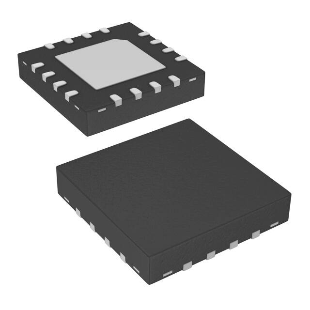


 工商网监
湘ICP备2023018690号
工商网监
湘ICP备2023018690号
