DATASHEET
HIP9011
FN4367
Rev 2.00
January 6, 2006
Engine Knock Signal Processor
The HIP9011 is used to provide a method of detecting
premature detonation often referred to as “Knock or Ping” in
internal combustion engines.
The IC is shown in the Simplified Block Diagram. The chip
can select between one of two sensors, if needed for
accurate monitoring or for “V” type engines. Internal control
via the SPI bus is fast enough to switch sensors between
each firing cycle. A programmable bandpass filter
processes the signal from either of the sensor inputs. The
bandpass filter can be selected to optimize the extraction
the engine knock or ping signals from the engine
background noise. Further single processing is obtained by
full wave rectification of the filtered signal and applying it to
an integrator whose output voltage level is proportional to
the knock signal amplitude. The chip is under
microprocessor control via a SPI interface bus.
PART
MARKING
HIP9011AB
HIP9011AB
HIP9011ABZ HIP9011ABZ
(See Note)
• Two Sensor Inputs
• Microprocessor Programmable
• Accurate and Stable Filter Elements
• Digitally Programmable Gain
• Digitally Programmable Time Constants
• Digitally Programmable Filter Characteristics
• On-Chip Crystal Oscillator
• Programmable Frequency Divider
• External Clock Frequencies up to 24MHz
- 4, 5, 6, 8, 10, 12, 16, 20, and 24MHz
• Operating Temperature Range -40oC to 125oC
• Pb-Free Plus Anneal Available (RoHS Compliant)
Ordering Information
PART
NUMBER
Features
Applications
TEMP.
RANGE
(oC)
PACKAGE
PKG.
DWG. #
-40 to 125
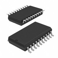
20 Ld SOIC
M20.3
-40 to 125
20 Ld SOIC
(Pb-free)
M20.3
• Engine Knock Detector Processor
• Analog Signal Processing Where Controllable Filter
Characteristics are Required
Add “T” suffix for tape and reel.
NOTE: Intersil Pb-free plus anneal products employ special Pb-free
material sets; molding compounds/die attach materials and 100%
matte tin plate termination finish, which are RoHS compliant and
compatible with both SnPb and Pb-free soldering operations. Intersil
Pb-free products are MSL classified at Pb-free peak reflow
temperatures that meet or exceed the Pb-free requirements of
IPC/JEDEC J STD-020.
Simplified Block Diagram
CH0NI
-
+
CH1FB
CH1IN
CH1NI
-
+
3RD ORDER
ANTIALIASING FILTER
CH0IN
CHANNEL SELECT
SWITCHES
CH0FB
PROGRAMMABLE
GAIN
STAGE
2- 0.111
64 STEPS
PROGRAMMABLE
BANDPASS
FILTER
1-20kHz
64 STEPS
ACTIVE
FULL WAVE
RECTIFIER
PROGRAMMABLE
INTEGRATOR
40 - 600s
32 STEPS
PROGRAMMABLE
DIVIDER
TO SWITCHED
CAPACITOR
NETWORKS
POWER SUPPLY
AND
BIAS CIRCUITS
VMID
FN4367 Rev 2.00
January 6, 2006
VDD
GND
REGISTERS
AND
STATE MACHINE
SPI
INTERFACE
OUTPUT
DRIVER INTOUT
AND
SAMPLE
AND HOLD
OSCIN
CLOCK OSCOUT
SCK
CS
SI
SO
INT/HOLD
TEST
Page 1 of 11
�HIP9011
Pinout
HIP9011
(SOIC)
TOP VIEW
VDD
1
20 CH0NI
GND
2
19 CH0IN
VMID
3
18 CH0FB
INTOUT
4
17 CH1FB
NC
5
16 CH1IN
NC
6
15 CH1NI
INT/HOLD
7
14 TEST
CS
8
13 SCK
OSCIN
9
12 SI
OSCOUT 10
11
SO
Pin Descriptions
PIN
NUMBER
DESIGNATION
1
VDD
Five volt power input.
2
GND
This pin is tied to ground.
3
VMID
This pin is connected to the internal mid-supply generator and is brought out for bypassing by a 0.022F capacitor.
4
INTOUT
Buffered output of the integrator. Output signal is held by an internal Sample and Hold circuit when INT/HOLD is
low.
5, 6
NC
7
INT/HOLD
8
CS
9
OSCIN
10
OSCOUT
11
SO
Output of the chip SPI data bus. This is a three-state output that is controlled via the SPI bus. The output is
placed in the high impedance state by setting CS high when the chip is not selected. This high impedance state
can also be programmed by setting the LSB of the prescaler word to 1. This will take precedence over CS. A 0
enables the active state. The Diagnostic Mode overrides these conditions.
12
SI
Input of the chip SPI data bus. Data length is eight bits. This pin has an internal pull-up.
13
SCK
Input from the SPI clock. Normally low, the data is transferred to the chip internal circuitry on the falling clock
edge. This pin has an internal pull up.
14
TEST
A low on this pin places the chip in the diagnostic mode. For normal operation this pin is tied high or left open.
This pin has an internal pull up.
15
CH1NI
Non-inverting input of Channel one.
16
CH1IN
Inverting input to channel one amplifier. A resistor is tied from this summing input to the transducer. A second
resistor is tied between this pin and pin 17, CH1FB to establish the gain of the amplifier.
17
CH1FB
Output of the channel one amplifier. This pin is used to apply feedback.
18
CH0FB
Output of the channel zero amplifier. This pin is used to apply feedback.
19
CH0IN
Inverting input to channel zero amplifier. Remainder same as channel one amplifier except feedback is applied
from pin 18.
20
CH0NI
Non-inverting input of Channel 0. Remainder the same as pin 16, except feedback is applied from terminal 18.
FN4367 Rev 2.00
January 6, 2006
DESCRIPTION
These pins are not internally connected. Do Not Use.
Selects whether the chip is in the Integrate Mode (Input High) or in the Hold Mode (Input Low). This pin has an
internal pull down.
A low input on this pin enables the chip to communicate over the SPI bus. This pin has an internal pull-up.
Input to inverter used for the oscillator circuit. A 4MHz crystal or ceramic resonator is connected between this pin and
pin 10. To bias the inverter, a 1.0M to 10M resistor is usually connected between this pin and pin 10.
Output of the inverter used for the oscillator. See pin 9 above.
Page 2 of 11
�HIP9011
Absolute Maximum Ratings
Thermal Information
DC Logic Supply, VDD . . . . . . . . . . . . . . . . . . . . . . . . . -0.5V to 7.0V
Output Voltage, VO . . . . . . . . . . . . . . . . . . . . . . . . . . . -0.5V to 7.0V
Input Voltage, VIN . . . . . . . . . . . . . . . . . . . . . . . . . . . . . . . . . 7V Max
Thermal Resistance (Typical, Note 1)
Operating Conditions
Temperature Range . . . . . . . . . . . . . . . . . . . . . . . . . -40oC to 125oC
JA (oC/W)
SOIC Package . . . . . . . . . . . . . . . . . . . . . . . . . . . . .
120
Maximum Power Dissipation, PD
For TA = -40oC to 70oC . . . . . . . . . . . . . . . . . . . . . . . 400mW Max
For TA = 70oC to 125oC, Derate Linearly at . . . . . . . . . . 6mW/oC
Maximum Junction Temperature . . . . . . . . . . . . . . . . . . . . . . .150oC
Maximum Storage Temperature Range, TSTG . . . . -65oC to 150oC
Maximum Lead Temperature (Soldering 10s) . . . . . . . . . . . . .300oC
At a Distance 1/16 1/32 inch, (1.59 0.79mm) from Case for
10s Max. (SOIC - Lead Tips Only)
CAUTION: Stresses above those listed in “Absolute Maximum Ratings” may cause permanent damage to the device. This is a stress only rating and operation of the
device at these or any other conditions above those indicated in the operational sections of this specification is not implied.
NOTE:
1. JA is measured with the component mounted on an evaluation PC board in free air.
VDD = 5V 5%, GND = 0V, Clock Frequency 4MHz 0.1%, TA = -40oC to 125oC,
Unless Otherwise Specified
Electrical Specifications
PARAMETER
SYMBOL
TEST CONDITIONS
MIN
TYP
MAX
UNITS
-
5.0
8.0
mA
DC ELECTRICAL SPECIFICATIONS
Quiescent Supply Current
IDD
VDD = 5.25V, GND = 0V
Midpoint Voltage, Pin 3
VMID
VDD = 5.0V, IL = 2mA Source
2.3
2.45
2.55
V
Midpoint Voltage, Pin 3
VMID
VDD = 5.0V, IL = 0mA
2.4
2.5
2.6
V
Low Input Voltage, Pins INT/HOLD, CS, SI, SCK
VIL
-
-
30
% of VDD
High Input Voltage, Pins INT/HOLD, CS, SI, SCK
VIH
70
-
-
% of VDD
Hysteresis voltage, Pins INT/HOLD, CS, SI, SCK
VHYST
0.85
-
-
V
-
50
-
A
I Source CS, SI, VDD = 5.0V, Measured at GND
SCK, TEST
Internal Pull-Up Current
Internal Pull-Down Current
I Sink,
INT/HOLD
VDD = 5.0V, Measured at VDD
-
-50
-
A
Low Level Output, Pin SO
VOL
ISOURCE = 1.6mA, VDD = 5.0V
0.01
-
0.30
V
High Level Output, Pin SO
VOH
ISINK = 200A, VDD = 5.0V
4.8
4.9
5.0
V
IL
Measured at GND; VDD = 5.0V
-
-
10
A
Low Level Output, Pin 10, OSCOUT
VOL
ISOURCE = 500A; VDD = 5.0V
-
-
1.5
V
High Level Output, Pin 10, OSCOUT
VOH
ISINK = -500A; VDD = 5.0V
4.4
-
-
V
Three-State Leakage Pin SO
SPI BUS INTERFACE
AC Parametrics
CS Falling to SCLK Rising
tCCH
10
-
-
ns
CS Rising to SCLK Falling
tCCL
80
-
-
ns
SCLK Low
tPWL
60
-
-
ns
SCLK High
tPWH
60
-
-
ns
SCLK Falling to CS Rising
tSCCH
60
-
-
ns
Data High Setup Time
tSUH
20
-
-
ns
Data Low Setup Time
tSUL
20
-
-
ns
Data High Hold Time
tHH
10
-
-
ns
Data Low Hold Time
tHL
10
-
-
ns
Min Time Between 2 Programmed Words
tCSH
200
-
-
ns
CS Rising to INT/Hold Rising
tCIH
8
-
-
s
FN4367 Rev 2.00
January 6, 2006
Page 3 of 11
�HIP9011
Electrical Specifications
VDD = 5V 5%, GND = 0V, Clock Frequency 4MHz 0.1%, TA = -40oC to 125oC,
Unless Otherwise Specified (Continued)
PARAMETER
SYMBOL
TEST CONDITIONS
MIN
TYP
MAX
UNITS
4.7
4.9
-
V
-
15
200
mV
+18
+20
+21
dB
INPUT AMPLIFIERS
CH0 and CH1 High Output Voltage
VOUTHI
ISINK = 100A, VDD = 5.0V
CH0 and CH1 Low Output Voltage
VOUTLO
ISOURCE = 100A; VDD = 5.0V
Voltage Gain
ACL
Input R = 47.5K, Feedback
R = 475k
BW
Test Mode
-
-0.5
-
dB
ATTEN
Test Mode
-10
-15
-
dB
VOUT
Run Mode
3.5
4.0
-
VP-P
Q
Run Mode
-
2.5
-
Q
%G
Run Mode
-
1
-
%
75
125
175
mV
ANTIALIASING FILTER
Response 1kHz to 20kHz, Referenced to 1kHz
Attenuation at 180kHz, Referenced
to 1kHz
PROGRAMMABLE FILTERS
Peak to Peak Voltage Output
Filters Q (Note 2)
PROGRAMMABLE GAIN AMPLIFIERS
Percent Amplifier Gain Deviation
INTEGRATOR
Integrator Reset Voltage
VRESET
Pin 4 Voltage at Start of
Integration
Cycle; VDD = 5.0V
Integrator Droop after 500s
VDROOP
Hold Mode, Pin 7 = 0V,
VDD = 5.0V
Pin 4 set to 20% to 80% of VDD
-
3
50
mV
DIFFERENTIAL CONVERTER
Differential to Single Ended Converter Offset
Voltage
DIFVIO
By Design
-
0.1
-
mV
Change In Converter Output
DIFOUT
Run Mode, 500A Sinking Load
to No Load Condition
-
1
10
mV
VOUT VRESET
Run Mode, maximum signal
output from Input Amplifier