HN27C101AG Series
HN27C301AG Series
131072-word × 8-bit CMOS UV Erasable and Programmable ROM
Description
The Hitachi HN27C101AG/HN27C301AG is a 1-Mbit ultraviolet erasable and electrically programmable
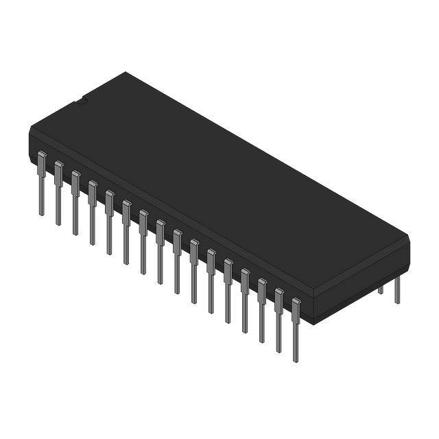
ROM. This device is packaged in a 32-pin dual-in-line package with transparent lid. The transparent lid
allows the memory content to be erased with ultraviolet light, whereby a new pattern can then be written into
the device.
Features
• Single power supply:
+5 V ± 5% (HN27C101AG-10/HN27C301AG-10)
+5 V ± 10% (HN27C101AG/HN27C301AG-12/15/17/20/ 25)
• Fast high-reliability programming mode and fast high-reliability page programming mode
Programming voltage: +12.5 V DC
Fast high-reliability page programming: 14 sec typ
• High speed inputs and outputs TTL compatible during both read and program modes
• Low power dissipation: 50 mW/MHz typ (active)
5 µW typ (standby)
• Pin arrangement : 32-pin JEDEC standard (HN27C101AG)
: replaceable 32 pin MASK ROM (HN27C301AG)
• Device identifier mode: manufacturer code and device code
• Fully compatible with HN27C101G/ HN27C301G series
�HN27C101AG/HN27C301AG Series
Ordering Information
Type No.
Access Time
Package
HN27C101AG-10
HN27C101AG-12
HN27C101AG-15
HN27C101AG-17
HN27C101AG-20
HN27C101AG-25
100 ns
120 ns
150 ns
170 ns
200 ns
250 ns
600-mil 32-pin cerdip (DG-32)
HN27C301AG-10
HN27C301AG-12
HN27C301AG-15
HN27C301AG-17
HN27C301AG-20
HN27C301AG-25
100 ns
120 ns
150 ns
170 ns
200 ns
250 ns
2
�HN27C101AG/HN27C301AG Series
Pin Arrangement
HN27C101AG Series
VPP
A16
A15
A12
A7
A6
A5
A4
A3
A2
A1
A0
I/O0
I/O1
I/O2
VSS
32
31
30
29
28
27
26
25
24
23
22
21
20
19
18
17
1
2
3
4
5
6
7
8
9
10
11
12
13
14
15
16
HN27C301AG Series
VCC
PGM
NC
A14
A13
A8
A9
A11
OE
A10
CE
I/O7
I/O6
I/O5
I/O4
I/O3
(Top view)
VPP
OE
A15
A12
A7
A6
A5
A4
A3
A2
A1
A0
I/O0
I/O1
I/O2
VSS
1
2
3
4
5
6
7
8
9
10
11
12
13
14
15
16
32
31
30
29
28
27
26
25
24
23
22
21
20
19
18
17
VCC
PGM
NC
A14
A13
A8
A9
A11
A16
A10
CE
I/O7
I/O6
I/O5
I/O4
I/O3
(Top view)
Pin Description
Pin Name
Function
A0 – A16
Address
I/O0 – I/O7
Input/output
CE
Chip enable
OE
Output enable
VCC
Power supply
VPP
Programming power supply
VSS
Ground
PGM
Programming enable
NC
No connection
3
�HN27C101AG/HN27C301AG Series
Block Diagram
A5
A9
A12
1024 × 1024
Memory Matrix
X-Decoder
A16
I/O0
Input
Data
Control
I/O7
Y-Gating
Y-Decoder
CE
OE
A0 – A4
PGM
A10, A11
VCC
VPP
VSS
4
H
H
: High Threshold Inverter
�HN27C101AG/HN27C301AG Series
Mode Selection
Mode
CE
OE
PGM
A9
VPP
VCC
I/O
HN27C101AG
(22)
(24)
(31)
(26)
(1)
(32)
(13 – 15, 17 – 21)
HN27C301AG
(22)
(2)
(31)
(26)
(1)
(32)
(13 – 15, 17 – 21)
Read
VIL
VIL
VIH
X
VCC
VCC
Dout
Output disable
VIL
VIH
VIH
X
VCC
VCC
High-Z
Standby
VIH
X
X
X
VCC
VCC
High-Z
Program
VIL
VIH
VIL
X
VPP
VCC
Din
Program verify
VIL
VIL
VIH
X
VPP
VCC
Dout
Page data latch
VIH
VIL
VIH
X
VPP
VCC
Din
Page program
VIH
VIH
VIL
X
VPP
VCC
High-Z
Program inhibit
VIL
VIL
VIL
X
VPP
VCC
High-Z
VIL
VIH
VIH
VIH
VIL
VIL
VIH
VIH
VIH
VIL
VIL
VIH
VH
VCC
VCC
Code
Identifier
Notes: 1. X: Don’t care
2. VH : 12.0 V ± 0.5 V
Absolute Maximum Ratings
Parameter
Symbol
All input and output voltages*
1
1
A9 input voltage*
Vin, Vout
Value
Unit
2
V
2
–0.6* to +7.0
VID
–0.6* to +13.5
V
1
VPP
–0.6 to +13.5
V
1
VCC voltage*
VCC
–0.6 to +7.0
V
Operating temperature range
Topr
0 to +70
°C
Storage temperature range
Tstg
–65 to +125
°C
Storage temperature range under bias
Tbias
–10 to +80
°C
VPP voltage*
Notes: 1. Relative to VSS
2. Vin, Vout and VID min = –1.0 V for pulse width ≤ 50 ns
5
�HN27C101AG/HN27C301AG Series
Capacitance (Ta = 25°C, f = 1 MHz)
Parameter
Symbol
Min
Typ
Max
Unit
Test Conditions
Input capacitance
Cin
—
—
10
pF
Vin = 0 V
Output capacitance
Cout
—
—
15
pF
Vout = 0 V
Read Operation
DC Characteristics (V CC = 5 V ± 5%, VPP = VCC, Ta = 0 to +70°C) (HN27C101AG/HN27C301AG-10)
(V CC = 5 V ± 10%, VPP = VCC, Ta = 0 to +70°C)
(HN27C101AG/HN27C301AG-12/15/17/20/25)
Parameter
Symbol
Min
Typ
Max
Unit
Test Conditions
Input leakage current
I LI
—
—
2
µA
Vin = 0 V to VCC
Output leakage current
I LO
—
—
2
µA
Vout = 0 V to VCC
VPP current
I PP1
—
1
20
µA
VPP = 5.5 V
Standby V CC current
I SB1
—
—
1
mA
CE = VIH
I SB2
—
1
20
µA
CE = VCC ± 0.3 V
I CC1
—
—
30
mA
CE = VIL, Iout = 0 mA
I CC2
—
—
30
mA
f = 5 MHz, Iout = 0 mA
—
50
mA
f = 10 MHz, Iout = 0 mA
Operating VCC current
—
1
Input low voltage
VIL
–0.3*
—
0.8
V
Input high voltage
VIH
2.2
—
VCC +
1.0*2
V
Output low voltage
VOL
—
—
0.45
V
I OL = 2.1 mA
Output high voltage
VOH
2.4
—
—
V
I OH = –1 mA
VCC – 0.7
—
—
V
I OH = –0.1 mA
Notes: 1. VIL min = –1.0 V for pulse width ≤ 50 ns
2. VIH max = VCC +1.5 V for pulse width ≤ 20 ns
If V IH is over the specified maximum value, read operation cannot be guaranteed.
6
�HN27C101AG/HN27C301AG Series
AC Characteristics (V CC = 5 V ± 5%, VPP = VCC, Ta = 0 to +70°C) (HN27C101AG/HN27C301AG-10)
(V CC = 5 V ± 10%, VPP = VCC, Ta = 0 to +70°C)
(HN27C101AG/HN27C301AG-12/15/17/20/25)
Test Conditions
•
•
•
•
Input pulse levels: 0.45 V to 2.4 V
Input rise and fall time: ≤ 20 ns
Output load: 1 TTL gate +100 pF
Reference levels for measuring timing: Inputs; 0.8 V and 2.0 V
Outputs; 0.8 V and 2.0 V
HN27C101AG/HN27C301AG
-10
Parameter
-12
-15
-17
-20
-25
Test
Symbol Min Max Min Max Min Max Min Max Min Max Min Max Unit Conditions
Address to
t ACC
output delay
—
100 —
120 —
150 —
170 —
200 —
250 ns
CE = OE =
VIL
CE to output t CE
delay
—
100 —
120 —
150 —
170 —
200 —
250 ns
OE = VIL
OE to output t OE
delay
—
60
—
60
—
70
—
70
—
70
—
100 ns
CE = VIL
OE high to
output float
t DF
0
50
0
50
0
50
0
50
0
50
0
60
ns
CE = VIL
Address to
output hold
t OH
0
—
0
—
0
—
0
—
0
—
0
—
ns
CE = OE =
VIL
Note: t DF is defined as the time at which the output achieves the open circuit condition and data is no longer
driven.
7
�HN27C101AG/HN27C301AG Series
Read Timing Waveform
Address
CE
Standby Mode
Active Mode
Standby Mode
tCE
OE
tDF
tOE
tACC
Data Out
8
tOH
Data Out Valid
�HN27C101AG/HN27C301AG Series
Fast High-Reliability Programming
This device can be applied the programming algorithm shown in following flowchart. This algorithm allows
to obtain faster programming time without any voltage stress to the device nor deterioration in reliability of
programmed data.
START
SET PROG./VERIFY MODE
VPP = 12.5 ± 0.3 V, VCC = 6.0 ± 0.25 V
Address = 0
n=0
n+1
n
Program tOPW = 0.2 ms ± 5%
Address + 1
Address
VERIFY
NOGO
GO
Program tOPW = 0.2n ms
n = 25
NO
YES
NO
LAST
Address?
YES
SET READ MODE
VCC = 5.0 ± 0.25 V, VPP = VCC
READ
All Address
NOGO
GO
END
FAIL
Fast High-Reliability Programming Flowchart
9
�HN27C101AG/HN27C301AG Series
DC Characteristics (Ta = 25 °C ± 5°C, VCC = 6 V ± 0.25 V, VPP = 12.5 V ± 0.3 V)
Parameter
Symbol
Min
Typ
Max
Unit
Test Conditions
Input leakage current
I LI
—
—
2
µA
Vin = 0 V to VCC
VPP supply current
I PP
—
—
40
mA
CE = PGM = VIL
Operating VCC current
I CC
—
—
30
mA
—
0.8
Input low level
VIL
5
–0.1*
V
6
Input high level
VIH
2.2
—
VCC + 0.5* V
Output low voltage during verify
VOL
—
—
0.45
V
I OL = 2.1 mA
Output high voltage during verify
VOH
2.4
—
—
V
I OH = –400 µA
Notes: 1. VCC must be applied simultaneously or before VPP and removed simultaneously or after V PP .
2. VPP must not exceed 13.5 V including overshoot.
3. An influence may be had upon device reliability if the device is installed or removed while V PP =
12.5 V.
4. Do not alter VPP either V IL to 12.5 V or 12.5 V to VIL when CE = Low.
5. VIL min = –0.6 V for pulse width ≤ 20 ns
6. If V IH is over the specified maximum value, programming operation cannot be guaranteed.
10
�HN27C101AG/HN27C301AG Series
AC Characteristics (Ta = 25°C ± 5°C, VCC = 6 V ± 0.25 V, VPP = 12.5 V ± 0.3 V)
Test Conditions
• Input pulse levels: 0.45 V to 2.4 V
• Input rise and fall time: ≤ 20 ns
• Reference levels for measuring timing: Inputs; 0.8 V and 2.0 V
Outputs; 0.8 V and 2.0 V
Parameter
Symbol
Min
Typ
Max
Unit
Address setup time
t AS
2
—
—
µs
OE setup time
t OES
2
—
—
µs
Data setup time
t DS
2
—
—
µs
Address hold time
t AH
0
—
—
µs
Data hold time
t DH
2
—
—
µs
0
—
130
ns
1
OE to output float delay
t DF *
VPP setup time
t VPS
2
—
—
µs
VCC setup time
t VCS
2
—
—
µs
PGM initial programming pulse
width
t PW
0.19
0.2
0.21
ms
PGM overprogramming pulse width t OPW* 2
0.19
—
5.25
ms
CE setup time
t CES
2
—
—
µs
Data valid from OE
t OE
0
—
150
ns
Test Conditions
Notes: 1. t DF is defined as the time at which the output achieves the open circuit condition and data is no
longer driven.
2. Refer to the programming flowchart for tOPW.
11
�HN27C101AG/HN27C301AG Series
Fast High-Reliability Programming Timing Waveform
Program
Program Verify
Address
tAS
Data
tAH
Data In Stable
tDS
VPP
Data Out Valid
tDH
tDF
VPP
VCC
tVPS
VCC
VCC+1
VCC
tVCS
CE
tCES
PGM
tPW
OE
12
tOES
tOE
�HN27C101AG/HN27C301AG Series
Fast High-Reliability Page Programming
This device can be applied the high performance page programming algorithm shown in following flowchart.
This algorithm allows to obtain faster programming time without any voltage stress to the device nor
deterioration in reliability of programmed data.
START
SET PAGE PROG. LATCH MODE
VPP = 12.5 ± 0.3 V, VCC = 6.0 ± 0.25 V
Address = 0
A
n=0
Latch
Address + 1
Address
n+1
Address + 1
Address
VERIFY
B
NO
A
YES
NOGO
GO
Program tOPW = 0.2n ms
Address + 1
Address
Latch
n = 25
Program tPW = 0.2 ms ± 5%
Address + 1
Address
B
NO
SET PAGE PROG./
VERIFY MODE
VPP = 12.5 ± 0.3 V,
VCC = 6.0 ± 0.25 V
Latch
Latch
n
LAST
Address?
YES
SET READ MODE
VCC = 5.0 ± 0.25 V, VPP = VCC
READ
All Address
NOGO
GO
END
FAIL
Fast High-Reliability Page Programming Flowchart
13
�HN27C101AG/HN27C301AG Series
DC Characteristics (Ta = 25 °C ± 5°C, VCC = 6 V ± 0.25 V, VPP = 12.5 V ± 0.3 V)
Parameter
Symbol Min
Input leakage current
I LI
VPP supply current
Operating VCC current
Input low level
Typ
Max
Unit
Test Conditions
—
—
2
µA
Vin = 0 V to VCC
I PP
—
—
50
mA
CE = OE= VIH, PGM = VIL
I CC
—
—
30
mA
—
0.8
VIL
5
–0.1*
V
6
Input high level
VIH
2.2
—
VCC + 0.5* V
Output low voltage during verify
VOL
—
—
0.45
V
I OL = 2.1 mA
2.4
—
—
V
I OH = –400 µA
Output high voltage during verify VOH
Notes: 1. VCC must be applied simultaneously or before VPP and removed simultaneously or after V PP .
2. VPP must not exceed 13.5 V including overshoot.
3. An influence may be had upon device reliability if the device is installed or removed while VPP =
12.5 V.
4. Do not alter VPP either V IL to 12.5 V or 12.5 V to VIL when CE = Low.
5. VIL min = –0.6 V for pulse width ≤ 20 ns
6. If V IH is over the specified maximum value, programming operation cannot be guaranteed.
14
�HN27C101AG/HN27C301AG Series
AC Characteristics (Ta = 25°C ± 5°C, VCC = 6 V ± 0.25 V, VPP = 12.5 V ± 0.3 V)
Test conditions
• Input pulse levels: 0.45 V to 2.4 V
• Input rise and fall time: ≤ 20 ns
• Reference levels for measuring timing: Inputs; 0.8 V and 2.0 V
Outputs; 0.8 V and 2.0 V
Parameter
Symbol
Min
Typ
Max
Unit
Address setup time
t AS
2
—
—
µs
OE setup time
t OES
2
—
—
µs
Data setup time
t DS
2
—
—
µs
Address hold time
t AH
0
—
—
µs
t AHL
2
—
—
µs
2
—
—
µs
0
—
130
ns
Data hold time
t DH
1
OE to output float delay
t DF *
VPP setup time
t VPS
2
—
—
µs
VCC setup time
t VCS
2
—
—
µs
PGM initial programming pulse width
t PW
0.19
0.2
0.21
ms
0.19
—
5.25
ms
2
PGM overprogramming pulse width
t OPW*
CE setup time
t CES
2
—
—
µs
Data valid from OE
t OE
0
—
150
ns
OE pulse width during data latch
t LW
1
—
—
µs
PGM setup time
t PGMS
2
—
—
µs
CE hold time
t CEH
2
—
—
µs
OE hold time
t OEH
2
—
—
µs
Notes: 1. t DF is defined as the time at which the output achieves the open circuit condition and data is no
longer driven.
2. Refer to the programming flowchart for tOPW.
15
�HN27C101AG/HN27C301AG Series
Fast High-Reliability Page Programming Timing Waveform
Page data latch
Page program
program verify
A2 to A16
tAS
tAHL
tDS
tDH
tAH
A0, A1
tPGMS
tOE
tDF
Data
Data in stable
VPP
VCC
VPP
VCC
VCC+1
VCC
Data out valid
tVPS
tVCS
tCES
tOEH
CE
tCEH
tPW
PGM
tOES
OE
tLW
Erase
Erasure of this device is performed by exposure to ultraviolet light of 2537 Å and all the output data are
changed to “1” after this erasure procedure. The minimum integrated dose (i.e. UV intensity × exposure time)
for erasure is 15 W · sec/cm2.
16
�HN27C101AG/HN27C301AG Series
Mode Description
Device Identifier Mode
The device identifier mode allows the reading out of binary codes that identify manufacturer and type of
device, from outputs of EPROM. By this mode, the device will be automatically matched its own
corresponding programming algorithm, using programming equipment.
HN27C101AG Identifier Code
Identifier
A0
(12)
A9
(26)
I/O7
(21)
I/O6
(20)
I/O5
(19)
I/O4
(18)
I/O3
(17)
I/O2
(15)
I/O1
(14)
I/O0
(13)
Hex Data
Manufacturer code
VIL
VH
0
0
0
0
0
1
1
1
07
Device code
VIH
VH
0
0
1
1
1
0
0
0
38
HN27C301AG Identifier Code
Identifier
A0
(12)
A9
(26)
I/O7
(21)
I/O6
(20)
I/O5
(19)
I/O4
(18)
I/O3
(17)
I/O2
(15)
I/O1
(14)
I/O0
(13)
Hex Data
Manufacturer code
VIL
VH
0
0
0
0
0
1
1
1
07
Device code
VIH
VH
1
0
1
1
1
0
0
1
B9
Notes: 1. VH = 12.0 V ± 0.5 V
2. A1–A8, A10–A16, CE, OE = VIL, PGM = VIH
17
�HN27C101AG/HN27C301AG Series
Package Dimensions
HN27C101AG/HN27C301AG Series (DG-32)
Unit: mm
41.91
43.18 Max
32
14.66
15.51 Max
17
.89
φ8
1
16
1.32
15.24
2.54 ± 0.25
18
0.48 ± 0.10
2.54 Min 5.89 Max
0.38 Min
2.54 Max
0.11
0.25 +– 0.05
0 – 10°
�
很抱歉,暂时无法提供与“HN27C101AG12”相匹配的价格&库存,您可以联系我们找货
免费人工找货