DATASHEET
ICL7126
FN3084
Rev.5.00
Oct 25, 2004
3 1/2 Digit, Low Power, Single Chip A/D Converter
The ICL7126 is a high performance, very low power
31/2-digit, A/D converter. All the necessary active devices
are contained on a single CMOS IC, including seven
segment decoders, display drivers, reference, and clock.
The ICL7126 is designed to interface with a liquid crystal
display (LCD) and includes a backplane drive. The supply
current of 100A is ideally suited for 9V battery operation.
Features
The ICL7126 brings together an unprecedented combination
of high accuracy, versatility, and true economy. It features
auto-zero to less than 10V, zero drift of less than 1V/oC,
input bias current of 10pA maximum, and rollover error of
less than one count. The versatility of true differential input
and reference is useful in all systems, but gives the designer
an uncommon advantage when measuring load cells, strain
gauges and other bridge-type transducers. And finally the
true economy of single power operation allows a high
performance panel meter or multi-meter to be built with the
addition of only 10 passive components and a display.
• True Differential Input and Reference
The ICL7126 can be used as a plug-in replacement for the
ICL7106 in a wide variety of applications, changing only the
passive components.
• 8,000 Hours Typical 9V Battery Life
• Guaranteed Zero Reading for 0V Input on All Scales
• True Polarity at Zero for Precise Null Detection
• 1pA Typical Input Current
• Direct LCD Display Drive - No External Components
Required
• Pin Compatible With the ICL7106
• Low Noise - Less Than 15VP-P
• On-Chip Clock and Reference
• Low Power Dissipation Guaranteed Less Than 1mW
• No Additional Active Circuits Required
• Pb-Free Available (RoHS Compliant)
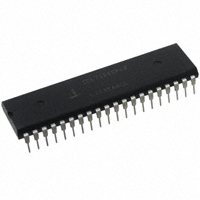
Pinout
ICL7126 (PDIP)
TOP VIEW
Ordering Information
TEMP. RANGE
PART NUMBER
(°C)
ICL7126CPL
ICL7126CPLZ
(Note 1)
0 to 70
0 to 70
PACKAGE
40 Ld PDIP
V+
1
40 OSC 1
D1
2
39 OSC 2
C1
3
38 OSC 3
B1
4
37 TEST
A1
5
36 REF HI
F1
6
35 REF LO
G1
7
34 CREF+
E1
8
D2
9
33 CREF32 COMMON
C2
10
31 IN HI
B2
11
30 IN LO
A2
12
29 A-Z
F2
13
28 BUFF
E2
14
27 INT
D3
15
26 V-
B3
16
25 G2 (10s)
F3
17
24 C3
E3
18
23 A3
(1000) AB4
19
22 G3
POL
(MINUS)
20
21 BP/GND
PKG.
DWG. #
E40.6
40 Ld PDIP
E40.6
(Pb-free) (Note 2)
(1s)
NOTES:
1. Intersil Pb-free products employ special Pb-free material sets;
molding compounds/die attach materials and 100% matte tin
plate termination finish, which are RoHS compliant and
compatible with both SnPb and Pb-free soldering operations.
Intersil Pb-free products are MSL classified at Pb-free peak
reflow temperatures that meet or exceed the Pb-free
requirements of IPC/JEDEC J STD-020C.
2. Pb-free PDIPs can be used for through hole wave solder
processing only. They are not intended for use in Reflow solder
processing applications.
FN3084 Rev.5.00
Oct 25, 2004
(10s)
(100s)
(100s)
Page 1 of 15
�ICL7126
Absolute Maximum Ratings
Thermal Information
Supply Voltage V+ to V- . . . . . . . . . . . . . . . . . . . . . . . . . . . . . . . 15V
Analog Input Voltage (Either Input) (Note 1) . . . . . . . . . . . . . V+ to VReference Input Voltage (Either Input) . . . . . . . . . . . . . . . . . V+ to VClock Input . . . . . . . . . . . . . . . . . . . . . . . . . . . . . . . . . . . TEST to V+
Thermal Resistance (Typical, Note 2)
Operating Conditions
Temperature Range . . . . . . . . . . . . . . . . . . . . . . . . . . . 0oC to 70oC
JA (oC/W)
PDIP Package . . . . . . . . . . . . . . . . . . . . . . . . . . . . .
50
Maximum Junction Temperature . . . . . . . . . . . . . . . . . . . . . . . 150oC
Maximum Storage Temperature Range . . . . . . . . . . -65oC to 150oC
Maximum Lead Temperature (Soldering 10s) . . . . . . . . . . . . . 300oC
NOTE: Pb-free PDIPs can be used for through hole wave solder
processing only. They are not intended for use in Reflow solder
processing applications.
CAUTION: Stresses above those listed in “Absolute Maximum Ratings” may cause permanent damage to the device. This is a stress only rating and operation of the
device at these or any other conditions above those indicated in the operational sections of this specification is not implied.
NOTES:
1. Input voltages may exceed the supply voltages provided the input current is limited to 100A.
2. JA is measured with the component mounted on an evaluation PC board in free air.
Electrical Specifications
TA = 25oC, VREF = 100mV, fCLOCK = 48kHz (Notes 1, 3)
PARAMETER
TEST CONDITIONS
MIN
TYP
MAX
UNITS
-000.0
000.0
+000.0
Digital
Reading
999
999/100
0
1000
Digital
Reading
SYSTEM PERFORMANCE
Zero Input Reading
VIN = 0.0V, Full Scale = 200mV
Ratiometric Reading
VlN = VREF , VREF = 100mV
Rollover Error
-VIN = +VlN 200mV
Difference in Reading for Equal Positive and Negative
Inputs Near Full Scale
-
0.2
1
Counts
Linearity
Full Scale = 200mV or Full Scale = 2V Maximum Deviation
from Best Straight Line Fit (Note 5)
-
0.2
1
Counts
Common Mode Rejection Ratio
VCM = 1V, VIN = 0V, Full Scale = 200mV (Note 5)
-
50
-
V/V
Noise
VIN = 0V, Full Scale = 200mV
(Peak-To-Peak Value Not Exceeded 95% of Time) (Note 5)
-
15
-
V
Leakage Current Input
VlN = 0V (Note 5)
-
1
10
pA
Zero Reading Drift
VlN = 0V, 0oC To 70oC (Note 5)
-
0.2
1
V/oC
Scale Factor Temperature Coefficient
VIN = 199mV, 0oC To 70oC,
(Ext. Ref. 0ppm/×oC) (Note 5)
-
1
5
ppm/oC
V+ Supply Current
VIN = 0V (Does Not Include COMMON Current)
-
70
100
A
COMMON Pin Analog Common Voltage
25k Between Common and Positive Supply
(With Respect to + Supply)
2.4
3.0
3.2
V
Temperature Coefficient of Analog Common
25k Between Common and Positive Supply
(With Respect to + Supply) (Note 5)
-
80
-
ppm/oC
Peak-To-Peak Segment Drive Voltage
Peak-To-Peak Backplane Drive Voltage
V+ = to V- = 9V (Note 4)
4
5.5
6
V
Power Dissipation Capacitance
vs Clock Frequency
-
40
-
pF
NOTES:
3. Unless otherwise noted, specifications are tested using the circuit of Figure 1.
4. Back plane drive is in phase with segment drive for ‘off’ segment, 180 degrees out of phase for ‘on’ segment. Frequency is 20 times conversion
rate. Average DC component is less than 50mV.
5. Not tested, guaranteed by design.
FN3084 Rev.5.00
Oct 25, 2004
Page 2 of 15
�ICL7126
Typical Application Schematics
-
9V
+
IN
-
+
750
R1
R5
240k 1M
0.047F
A3 23
BP 21
20 POL
C3 24
17 F3
G3 22
G2 25
16 B3
19 AB4
V- 26
15 D3
18 E3
INT 27
14 E2
A-Z 29
BUFF 28
IN HI 31
C1 = 0.1F
C2 = 0.22F
C3 = 0.047F
C4 = 50pF
C5 = 0.01F
R1 = 240k
R2 = 180k
R3 = 180k
R4 = 10k
R5 = 1M
DISPLAY
13 F2
0.01
C3
0.22F
C2 R2
IN LO 30
COM 32
CREF- 33
REF LO 35
TEST 37
C1 0.1F
REF HI 36
OSC 3 38
180k
OSC 2 39
OSC 1 40
R4
10k
C4
50pF
CREF+ 34
R3
180k
C5
12 A2
11 B2
D2
9
10 C2
E1
8
A1
5
F1
B1
4
G1
C1
3
7
D1
2
6
V+
1
ICL7126
DISPLAY
FIGURE 1. ICL7126 TEST CIRCUIT AND TYPICAL APPLICATION WITH LCD DISPLAY COMPONENTS SELECTED
FOR 200mV FULL SCALE
-
+
SET REF = 100.0mV
IN
9V
-
+
R1
R5
240k 1M
C5
V- 26
G2 25
C3 24
A3 23
G3 22
BP 21
16 B3
17 F3
18 E3
19 AB4
20 POL
INT 27
DISPLAY
15 D3
BUFF 28
14 E2
0.15F
C3
13 F2
A-Z 29
IN LO 30
180k
C2 R2
0.33F
0.01
IN HI 31
COM 32
CREF- 33
REF HI 36
C1 0.1F
REF LO 35
TEST 37
OSC 3 38
OSC 2 39
180k
OSC 1 40
R4
10k
C4
50pF
CREF+ 34
R3
B1
A1
F1
G1
E1
D2
4
5
6
7
8
9
11 B2
C1
3
12 A2
D1
2
10 C2
V+
1
ICL7126
C1 = 0.1F
C2 = 0.33F
C3 = 0.5F
C4 = 50pF
C5 = 0.01F
R1 = 240k
R2 = 180k
R3 = 180k
R4 = 10k
R5 = 1M
DISPLAY
FIGURE 2. ICL7126 CLOCK FREQUENCY 16kHz, 1 READING/S
FN3084 Rev.5.00
Oct 25, 2004
Page 3 of 15
�ICL7126
(Continued)
R1
240k
IN
-
+
+
9V
750
R5
1M
A3 23
BP 21
20 POL
C3 24
17 F3
G3 22
G2 25
16 B3
19 AB4
V- 26
15 D3
18 E3
0.047F
INT 27
14 E2
A-Z 29
DISPLAY
BUFF 28
180k
C3
13 F2
0.01
IN HI 31
C2 R2
IN LO 30
COM 32
CREF- 33
CREF+ 34
C1 0.1F
REF LO 35
TEST 37
REF HI 36
OSC 3 38
180k
OSC 2 39
OSC 1 40
R4
10k
C4
50pF
0.22F
C5
R3
-
Typical Application Schematics
B1
A1
F1
G1
E1
D2
4
5
6
7
8
9
12 A2
C1
3
11 B2
D1
2
10 C2
V+
1
ICL7126
C1 = 0.1F
C2 = 0.22F
C3 = 0.047F
C4 = 50pF
C5 = 0.01F
R1 = 240k
R2 = 180k
R3 = 180k
R4 = 10k
R5 = 1M
DISPLAY
FIGURE 3. CLOCK FREQUENCY 48kHz, 3 READINGS/S
FN3084 Rev.5.00
Oct 25, 2004
Page 4 of 15
�ICL7126
Design Information Summary Sheet
• OSCILLATOR FREQUENCY
fOSC = 0.45/RC
COSC > 50pF; ROSC > 50k
fOSC (Typ) = 48kHz
• DISPLAY COUNT
• OSCILLATOR PERIOD
tOSC = RC/0.45
• CONVERSION CYCLE
tCYC = tCL0CK x 4000
tCYC = tOSC x 16,000
when fOSC = 48KHz; tCYC = 333ms
V IN
COUNT = 1000 --------------V REF
• INTEGRATION CLOCK FREQUENCY
fCLOCK = fOSC /4
• COMMON MODE INPUT VOLTAGE
(V- + 1V) < VlN < (V+ - 0.5V)
• INTEGRATION PERIOD
tINT = 1000 x (4/fOSC)
• AUTO-ZERO CAPACITOR
0.01F < CAZ < 1F
• 60/50Hz REJECTION CRITERION
tINT /t60Hz or tlNT /t50Hz = Integer
• REFERENCE CAPACITOR
0.1F < CREF < 1F
• OPTIMUM INTEGRATION CURRENT
IINT = 4A
• FULL-SCALE ANALOG INPUT VOLTAGE
VlNFS (Typ) = 200mV or 2V
• INTEGRATE RESISTOR
V INFS
R INT = ----------------I INT
• VCOM
Biased between V+ and V• VCOM V+ - 2.8V
Regulation lost when V+ to V- < 6.8V;
If VCOM is externally pulled down to (V + to V -)/2,
the VCOM circuit will turn off
• ICL7126 POWER SUPPLY: SINGLE 9V
V+ - V- = 9V
Digital supply is generated internally
VTEST V+ - 4.5V
• INTEGRATE CAPACITOR
t INT I INT
C INT = -------------------------------V INT
• INTEGRATOR OUTPUT VOLTAGE SWING
t INT I INT
V INT = -------------------------------C INT
• ICL7126 DISPLAY: LCD
Type: Direct drive with digital logic supply amplitude
• VINT MAXIMUM SWING:
(V- + 0.5V) < VINT < (V+ - 0.5V), VINT (Typ) = 2V
Typical Integrator Amplifier Output Waveform (INT Pin)
AUTO ZERO PHASE
(COUNTS)
2999 - 1000
SIGNAL INTEGRATE
PHASE FIXED
1000 COUNTS
DE-INTEGRATE PHASE
0 - 1999 COUNTS
TOTAL CONVERSION TIME = 4000 x tCLOCK = 16,000 x tOSC
FN3084 Rev.5.00
Oct 25, 2004
Page 5 of 15
�ICL7126
Detailed Description
De-integrate Phase
The final phase is de-integrate, or reference integrate. Input
low is internally connected to analog COMMON and input high
is connected across the previously charged reference
capacitor. Circuitry within the chip ensures that the capacitor
will be connected with the correct polarity to cause the
integrator to output to return to zero. The time required for the
output to return to zero is proportional to the input signal.
Analog Section
Figure 4 shows the Functional Diagram of the Analog Section
for the ICL7126. Each measurement cycle is divided into three
phases. They are (1) auto-zero (A-Z), (2) signal integrate (INT)
and (3) de-integrate (DE).
Auto-Zero Phase
During auto-zero three things happen. First, input high and low
are disconnected from the pins and internally shorted to analog
COMMON. Second, the reference capacitor is charged to the
reference voltage. Third, a feedback loop is closed around the
system to charge the auto-zero capacitor CAZ to compensate
for offset voltages in the buffer amplifier, integrator, and
comparator. Since the comparator is included in the loop, the
A-Z accuracy is limited only by the noise of the system. In any
case, the offset referred to the input is less than 10V.
Specifically, the digital reading displayed is:
VIN
Display Count = 1000 --------------- .
VREF
Differential Input
The input can accept differential voltages anywhere within the
common mode range of the input amplifier, or specifically from
0.5V below the positive supply to 1V above the negative
supply. In this range, the system has a CMRR of 86dB typical.
However, care must be exercised to assure the integrator
output does not saturate. A worst case condition would be a
large positive common mode voltage with a near full-scale
negative differential input voltage. The negative input signal
drives the integrator positive when most of its swing has been
used up by the positive common mode voltage. For these
critical applications the integrator output swing can be reduced
to less than the recommended 2V full scale swing with little
loss of accuracy. The integrator output can swing to within 0.5V
of either supply without loss of linearity.
Signal Integrate Phase
During signal integrate, the auto-zero loop is opened, the
internal short is removed, and the internal input high and low
are connected to the external pins. The converter then
integrates the differential voltage between IN HI and IN LO for
a fixed time. This differential voltage can be within a wide
common mode range: up to 1V from either supply. If, on the
other hand, the input signal has no return with respect to the
converter power supply, IN LO can be tied to analog COMMON
to establish the correct common mode voltage. At the end of
this phase, the polarity of the integrated signal is determined.
CREF
RINT
CREF+
REF HI
34
36
V+
REF LO
35
A-Z
CREF33
28
A-Z
1
DE+
27
INTEGRATOR
-
+
2.8V
DE-
INT
29
-
31
INT
CINT
A-Z
+
1A
IN HI
CAZ
BUFFER V+
6.2V
INPUT
HIGH
A-Z
A-Z
COMMON
DE+
32
-
DE-
INPUT
LOW
A-Z AND DE
IN LO
COMPARATOR
+
N
TO
DIGITAL
SECTION
+
30
INT
26
V-
FIGURE 4. ANALOG SECTION OF ICL7126
FN3084 Rev.5.00
Oct 25, 2004
Page 6 of 15
�ICL7126
V+
V+
V+
V+
REF HI
6.8V
ZENER
REF LO
27k
200k
ICL7126
ICL7126
IZ
REF HI
REF LO
ICL8069
1.2V
REFERENCE
COMMON
V-
FIGURE 5B.
FIGURE 5A.
FIGURE 5.
Differential Reference
The reference voltage can be generated anywhere within the
power supply voltage of the converter. The main source of
common mode error is a roll-over voltage caused by the
reference capacitor losing or gaining charge to stray capacity on
its nodes. If there is a large common mode voltage, the
reference capacitor can gain charge (increase voltage) when
called up to de-integrate a positive signal but lose charge
(decrease voltage) when called up to de-integrate a negative
input signal. This difference in reference for positive or negative
input voltage will give a roll-over error. However, by selecting the
reference capacitor large enough in comparison to the stray
capacitance, this error can be held to less than 0.5 count worst
case. (See Component Value Selection.)
Analog COMMON
COMMON, a common mode voltage exists in the system and
is taken care of by the excellent CMRR of the converter.
However, in some applications IN LO will be set at a fixed
known voltage (power supply common for instance). In this
application, analog COMMON should be tied to the same
point, thus removing the common mode voltage from the
converter. The same holds true for the reference voltage. If
reference can be conveniently tied to analog COMMON, it
should be since this removes the common mode voltage from
the reference system.
Within the lC, analog COMMON is tied to an N channel FET
that can sink approximately 3mA of current to hold the voltage
2.8V below the positive supply (when a load is trying to pull the
common line positive). However, there is only 1A of source
current, so COMMON may easily be tied to a more negative
voltage thus overriding the internal reference.
This pin is included primarily to set the common mode voltage
for battery operation or for any system where the input signals
are floating with respect to the power supply. The COMMON
pin sets a voltage that is approximately 2.8V more negative
than the positive supply. This is selected to give a minimum
end-of-life battery voltage of about 6.8V. However, analog
COMMON has some of the attributes of a reference voltage.
When the total supply voltage is large enough to cause the
zener to regulate (