ICS9179B-01
Integrated
Circuit
Systems, Inc.
Low Skew Buffers
General Description
Features
The ICS9179B-01 generates SDRAM clock buffers
required for high speed RISC or CISC microprocessor
systems such as Intel PentiumPro or Pentium II. An
output enable is provided for testability.
•
The device is a buffer with low output to output skew. This
is a Fanout buffer device, not using an internal PLL. This
buffer can also be a feedback to an external PLL stage for
phase synchronization to a master clock.
•
The individual clock outputs are addressable through I2C
to be enabled, or stopped in a low state for reduced EMI
when the lines are not needed.
•
Block Diagram
•
•
•
•
•
•
High speed, low noise non-inverting (0:17) buffer for
SDRAM clock buffer applications.
Supports up to four SDRAM DIMMS
Synchronous clocks skew matched to 250 ps
window on SDRAM.
I2C Serial Configuration interface to allow individual
clocks to be stopped.
Multiple VDD, VSS pins for noise reduction
Tri-state pin for testing
Custom configurations available
3.0V – 3.7V supply range
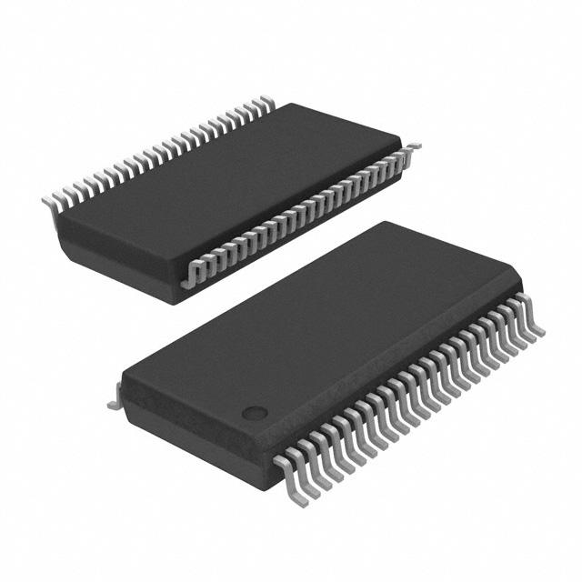
48-pin SSOP package
Pin Configuration
48-Pin SSOP
0256E—12/15/08
PentiumPro is a trademark of Intel Corporation
I2C is a trademark of Philips Corporation
�ICS9179B-01
Pin Descriptions
PIN NUMBER
PIN NAME
TYPE DESCRIPTION
4, 5, 8, 9
SDRAM (0:3)
OUT SDRAM Byte 0 clock outputs1
13, 14, 17, 18
SDRAM (4:7)
OUT SDRAM Byte 1 clock outputs1
31, 32, 35, 36 SDRAM (8:11) OUT SDRAM Byte 2 clock outputs1
40, 41, 44, 45 SDRAM (12:15) OUT SDRAM Byte 3 clock outputs1
21, 28
SDRAM (16:17) OUT SDRAM clock outputs useable for feedback.1
11
BUF_IN
IN Input for buffers
Tri-states all outputs when held LOW. Has internal
38
OE
IN pull-up.
2
24
SDATA
I/O Data pin for I2C circuitry3
25
SCLK
I/O Clock pin for I2C circuitry3
3, 7, 12, 16,
20, 29, 33, 37,
VDD
PWR 3.3V Power supply for SDRAM buffer
42, 46
6, 10, 15, 19,
22, 27, 30, 34,
GND
PWR Ground for SDRAM buffer
39, 43
23
VDDS
PWR 3.3V Power supply for I2C circuitry
26
GNDS
PWR Ground for I2C circuitry
1, 2, 47, 48
N/C
Pins are not internally connected
Notes:
1.
At power up all eighteen SDRAM outputs are enabled and active.
2.
OE has a 100K Ohm internal pull-up resistor to keep all outputs active.
3.
The SDATA and SCLK inputs both also have internal pull-up resistors with values above 100K Ohms as well
for complete platform flexibility.
Power Groups
VDD = Power supply for SDRAM buffer
VDDS = Power supply for I2C circuitry
Ground Groups
GND = Ground for SDRAM buffer
GNDS = Ground for I2C circuitry
2
�ICS9179B-01
Technical Pin Function Descriptions
VDD
This is the power supply to the internal core logic of the
device as well as the clock output buffers for
SDRAM(0:17).
This pin operates at 3.3V volts. Clocks from the listed
buffers that it supplies will have a voltage swing from
Ground to this level. For the actual guaranteed high and
low voltage levels for the Clocks, please consult the DC
parameter table in this data sheet.
GND
This is the power supply ground (common or negative)
return pin for the internal core logic and all the output
buffers.
SDRAM(0:17)
These Output Clocks are use to drive Dynamic RAM’s
and are low skew copies of the CPU Clocks. The voltage
swing of the SDRAM’s output is controlled by the supply
voltage that is applied to VDD of the device, operates at
3.3 volts.
I2C
The SDATA and SCLOCK Inputs are use to program the
device. The clock generator is a slave-receiver device in
the I2C protocol. It will allow read-back of the registers.
See configuration map for register functions. The I2C
specification in Philips I2C Peripherals Data Handbook
(1996) should be followed.
BUF_IN
Input for Fanout buffers (SDRAM 0:17).
OE
OE tristates all outputs when held low.
VDDS
This is the power supply to I2C circuitry.
GNDS
This is the ground to I2C circuitry.
3
�ICS9179B-01
General I2C serial interface information
A.
For the clock generator to be addressed by an I2C controller, the following address must be sent as a start
sequence, with an acknowledge bit between each byte.
Then Byte 0, 1, 2, etc in
sequence until STOP.
B.
The clock generator is a slave/receiver I2C component. It can "read back "(in Philips I2C protocol) the data stored
in the latches for verification. (set R/W# to 1 above). There is no BYTE count supported, so it does not meet
the Intel SMB PIIX4 protocol.
Byte 0, 1, 2, etc in sequence until STOP.
C.
The data transfer rate supported by this clock generator is 100K bits/sec (standard mode)
D.
The input is operating at 3.3V logic levels.
E.
The data byte format is 8 bit bytes.
F.
To simplify the clock generator I2C interface, the protocol is set to use only block writes from the controller. The
bytes must be accessed in sequential order from lowest to highest byte with the ability to stop after any complete
byte has been transferred. The Command code and Byte count shown above must be sent, but the data is ignored
for those two bytes. The data is loaded until a Stop sequence is issued.
G.
In the power down mode (PWR_DWN# Low), the SDATA and SCLK pins are tristated and the internal data latches
maintain all prior programming information.
H.
At power-on, all registers are set to a default condition. Bytes 0 through 2 default to a 1 (Enabled output state).
Serial Configuration Command Bitmaps
Byte 0: SDRAM Clock Register
Notes: 1 = Enabled; 0 = Disabled, outputs held low
Note: PWD = Power-Up Default
4
�ICS9179B-01
Functionality
Byte 1: SDRAM Clock Register
Byte 2: PCICLK Clock Register
BIT
PWDPWD
DESCRIPTION
BIT PIN#
PIN#
DESCRIPTION
SDRAM15
45
1 (Act/Inact)
SDRAM17
Bit 7 28
1 (Act/Inact)
SDRAM14
Bit 6
44
1 (Act/Inact)
SDRAM16
SDRAM13
Bit
1 1(Act/Inact)
Bit 5 6 41 21 Notes:
1 (Act/Inact)
= Enabled; 0 = Disabled,
SDRAM12
Bit 4 5 40 - 1 (Act/Inact)
Bit
1 Reserved
Note:
PWD = Power-Up Default
SDRAM11
Bit
1 Reserved
Bit 3 4 36 - 1 (Act/Inact))
Bit
1 Reserved
SDRAM10
2 2 3 35 Bit
1 (Act/Inact)
Bit 2
1 Reserved
SDRAM9
Bit 1
32
1 (Act/Inact)
Bit 1
1 Reserved
SDRAM8
Bit 0 0 31 - 1 (Act/Inact))
Bit
1 Reserved
OE#
Bit 7
0
Max 3.3V supply consumption
SDRAM (0:3)Max SDRAM
(4:7)loadsSDRAM (8:11)
discrete cap
Condition
Hi-Z
VDD = 3.465V
All static inputs
= VDD
GND
Hi-Zoutputs
Hi-Z
heldorlow
SDRAM
(12:15)
SDRAM
(16:17)
Hi-Z
Hi-Z
1 X BUF_IN
1 X BUF_IN
Notes: 1 = Enabled; 0 = Disabled, outputs held low
No Clock Mode
1 - VDD1
1 X BUF_IN
1 X BUF_IN
1 X BUF_IN
(BUF_IN
or
3mA
GND)
I C Circuitry Active
Active 66MHz
115mA
Power Management
(BUF_IN =ICS9179B-01
66.66MHz)
The values below are estimates of target specifications.
Active 100MHz
180mA
(BUF_IN = 100.00MHz)
5
�ICS9179B-01
Absolute Maximum Ratings
Supply Voltage . . . . . . . . . . . . . . . . . . . . . . . 7.0 V
Logic Inputs . . . . . . . . . . . . . . . . . . . . . . . . . GND –0.5 V to VDD +0.5 V
Ambient Operating Temperature . . . . . . . . . . 0°C to +70°C
Storage Temperature . . . . . . . . . . . . . . . . . . . –65°C to +150°C
Stresses above those listed under Absolute Maximum Ratings may cause permanent damage to the device. These
ratings are stress specifications only and functional operation of the device at these or any other conditions above those
listed in the operational sections of the specifications is not implied. Exposure to absolute maximum rating conditions
for extended periods may affect product reliability.
6
�ICS9179B-01
Electrical Characteristics - SDRAM
TA = 0 - 70C; VDD = VDDL = 3.3 V +/-5%; CL = 20 - 30 pF (unless otherwise stated)
PARAMETER
Output Impedance
Output Impedance
Output High Voltage
Output Low Voltage
Output High Current
Output Low Current
Rise Time1
SYMBOL
RDSP
RDSN
VOH
VOL
I OH
I OL
CONDITIONS
VO = VDD*(0.5)
VO = VDD*(0.5)
I OH = -36 mA
I OL = 23 mA
VOH = 2.0 V
VOL = 0.8 V
MIN
10
10
2.4
TYP
40
3
0.27
-115
57
MAX UNITS
24
W
24
W
V
0.4
V
-54
mA
mA
Tr
VOL = 0.4 V, VOH = 2.4 V
0.5
0.95
1.33
ns
Fall Time1
Tf
VOH = 2.4 V, VOL = 0.4 V
0.5
0.95
1.33
ns
Duty Cycle1
Dt
VT = 1.5 V
45
51
55
%
Tsk
TPROP
VT = 1.5 V
VT = 1.5 V
1
110
5
250
6
ps
ns
TPROPEN
TPROPDIS
VT = 1.5 V
VT = 1.5 V
1
1
8
8
ns
ns
1
Skew
1
Propagation
1
Guarenteed by design, not 100% tested in production.
7
�ICS9179B-01
General Layout Precautions:
1) Use a ground plane on the top
layer of the PCB in all areas not
used by traces.
2) Make all power traces and vias as
wide as possible to lower
inductance.
Notes:
1 All clock outputs should have
series terminating resistor. Not
shown in all places to improve
readibility of diagram
2 Optional EMI capacitor should be
used on all CPU, SDRAM, and PCI
outputs.
Capacitor Values:
All unmarked capacitors are 0.01µF ceramic
8
�ICS9179B-01
SSOP Package
SYMBOL
A
A1
A2
B
C
D
E
e
H
h
L
N
µ
X
COMMON DIMENSIONS
MIN.
NOM.
MAX.
.095
.101
.110
.008
.012
.016
.088
.090
.092
.008
.010
.0135
.005
.010
See Variations
.292
.296
.299
0.025 BSC
.400
.406
.410
.010
.013
.016
.024
.032
.040
See Variations
0°
5°
8°
.085
.093
.100
VARIATIONS
AC
MIN.
.620
D
NOM.
.625
Ordering Information
9179BF-01LF
Example:
XXXX F - PPP LF
denotes Pb-free configuration, RoHS compliant
Pattern Number (2 or 3 digit number for parts with ROM code
patterns)
Package Type
F=SSOP
Device Type
9
N
MAX.
.630
48
�ICS9179B-01
10
�