IDT5V9352
3.3V/2.5V PHASE-LOCK LOOP CLOCK DRIVER ZERO DELAY BUFFER
INDUSTRIAL TEMPERATURE RANGE
IDT5V9352
3.3V/2.5V PHASE-LOCK LOOP CLOCK
DRIVER ZERO DELAY BUFFER
PRODUCT DISCONTINUATION NOTICE - LAST TIME BUY EXPIRES OCT 28, 2014
FEATURES:
The 5V9352 features three banks of individually configurable outputs.
The banks are configured with five, four, and two outputs. The internal
divide circuitry allows for output frequency ratios of 1:1, 2:1, 3:1, and 3:2:1.
The output frequency relationship is controlled by the fSEL frequency
control pins. The fSEL pins, as well as other inputs, are LVCMOS/LVTTL
compatible inputs
Unlike many products containing PLLs, the 5V9352 does not require
external RC networks. The loop filter for the PLL is included on-chip,
minimizing component count, board space, and cost.
Because it is based on PLL circuitry, the 5V9352 requires a stabilization
time to achieve phase lock of the feedback signal to the reference signal.
This stabilization time is required, following power up and application of a
fixed-frequency, fixed-phase signal at REFCLK, as well as following any
changes to the PLL reference or feedback signals. The PLL can be
bypassed for test purposes by setting the PLL_EN to high.
The 5V9352 is available in Industrial temperature range (-40°C to
+85°C).
• Phase-lock loop clock distribution for high performance clock
tree applications
• Output enable bank control
• External feedback (FBIN) pin is used to synchronize the
outputs to the clock input signal
• No external RC network required for PLL loop stability
• Operates at 3.3V/2.5V VCC
• Spread Spectrum Compatible
• Operating frequency up to 200MHz
• Compatible with Motorola MPC9352
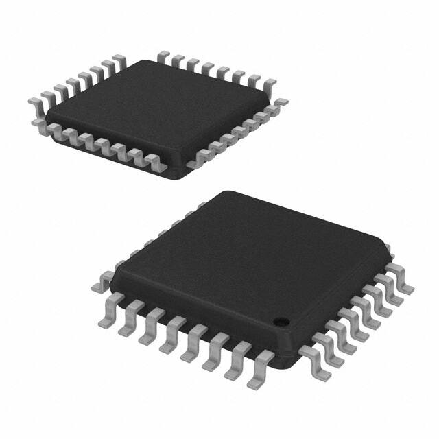
• Available in 32-pin TQFP package
• Use replacement part: 87952AYILF
DESCRIPTION:
The 5V9352 is a low-skew, low-jitter, phase-lock loop (PLL) clock driver
targeted for high performance clock tree applications. It uses a PLL to
precisely align, in both frequency and phase. The 5V9352 operates at 2.5V
and 3.3V.
FUNCTIONAL BLOCK DIAGRAM
BANK A
QA0
CCLK
1
REFCLK
REF
1
6
1
QA1
VCO
PLL
FBIN
2
0
0
4
0
QA2
FB
2
QA3
QA4
PLL_En
BANK B
QB0
VCO_SEL
1
QB1
0
fSELA
QB2
QB3
fSELB
BANK C
1
QC0
0
QC1
fSELC
MR/OE
The IDT logo is a registered trademark of Integrated Device Technology, Inc.
INDUSTRIAL TEMPERATURE RANGE
MAY 2013
1
c
2003
Integrated Device Technology, Inc.
DSC 5973/19
�IDT5V9352
3.3V/2.5V PHASE-LOCK LOOP CLOCK DRIVER ZERO DELAY BUFFER
INDUSTRIAL TEMPERATURE RANGE
VCC
QC1
QC0
GND
GND
QB3
QB2
VCC
PIN CONFIGURATION
32
31
30
29
28
27
26
25
fSELC
2
23
QB1
fSELB
3
22
QB0
fSELA
4
21
VCC
MR/OE
5
20
VCC
REFCLK
6
19
QA4
GND
7
18
QA3
FBIN
8
17
GND
12
QA0
VCCA
11
VCC
10
PLL_En
9
13
14
15
16
VCC
GND
QA2
24
QA1
1
GND
VCO_SEL
TQFP
TOP VIEW
CAPACITANCE
ABSOLUTE MAXIMUM RATINGS(1)
Symbol
VCC
Rating
Supply Voltage Range
Parameter
Description
Min.
Typ.
Max.
Unit
Max.
Unit
–0.3 to +3.6
V
CIN
Input Capacitance
⎯
4
⎯
pF
CPD
Power Dissipation
Capacitance
⎯
10
⎯
pF
VI
Input Voltage Range
–0.3 to VCC+0.3
V
IIN
Input Current
±20
mA
IOUT
DC Output Current
±50
mA
TSTG
Storage Temperature Range
–65 to +125
°C
LOGIC DIAGRAM(1,2)
NOTE:
1. Stresses beyond those listed under ABSOLUTE MAXIMUM RATINGS may cause
permanent damage to the device. These are stress rating only, and functional
operation of the device at these or any other conditions beyond those indicated
under “recommended operating conditions” is not implied. Exposure to absolutemaximum-rated conditions for extended periods may affect device reliability.
RF
VCCA
VCC
CF
10nF
GENERAL SPECIFICATIONS
Symbol
VTT
HBM
LU
Description
Min.
Output Termination Voltage
Typ.
VCC/2
VCC
Max. Unit
V
ESD Protection (human body model)
2000
V
Latch-Up Immunity
200
mA
33...100nF
NOTES:
1. IDT5V9352 requires an external RC filter for the analog power supply pin VCCA.
2. For VCC = 2.5V, RF = 9-10Ω, CF = 22μF.
For VCC = 3.3V, RF = 5-15Ω, CF = 22μF.
2
�IDT5V9352
3.3V/2.5V PHASE-LOCK LOOP CLOCK DRIVER ZERO DELAY BUFFER
INDUSTRIAL TEMPERATURE RANGE
FUNCTION TABLES
fSELA
QAn
fSELB
QBn
fSELC
QCn
Control Pin
Logic 0
0
÷4
0
÷4
0
÷2
VCO_SEL
fVCO
1
÷6
1
÷2
1
÷4
MR/OE
Output Enable
PLL_En
Enable PLL
Logic 1
fVCO / 2
Outputs disable (high-impedance state) and
reset of the device.
Disable PLL
NOTE:
1. IDT5V9352 requires reset at power up and after any loss of PLL lock. Length of reset
pulse should be greater than two REF CLK cycles (REFCLK).
PIN DESCRIPTION
Terminal
Name
No.
Type
REFCLK
6
I
FBIN
8
I
VCCA
10
PWR
GND
7, 13, 17, 24,
Ground
Description
Reference clock input
Feedback input.
Analog power supply
Negative power supply
28, 29
VCO_SEL
1
I
Allows for the choice of two VCO ranges to optimize PLL stability and jitter performance
MR/OE
5
I
Allows the user to force the outputs into HIGH impedence for board level test
QA (0:4)
12, 14, 15,
QB (0:3)
22, 23, 26, 27
O
Clock outputs. These outputs provide low skew copies of REFCLK or can be at different frequencies than REFCLK.
QC (0:1)
30, 31
VCC
11, 16, 20, 21,
18, 19
PWR
Positive power supply for I/O and core
25, 32
PLL_EN
9
I
PLL enable input. When set LOW, PLL is enabled. When set HIGH, PLL is disabled.
fSEL(C:A)
2, 3, 4
I
Frequency control pin
DC ELECTRICAL CHARACTERISTICS
TA = –40°C to +85°C, VCC = 3.3V ± 5%
Parameter
Description
Test Conditions
Min.
Typ.(1)
Unit
VCC + 0.3
V
0.8
V
V
VIH
Input HIGH Level
VIL
Input LOW Level
VOH
HIGH Level Output Voltage
IOH = –24mA
VOL
LOW Level Output Voltage
IOL = 12mA
0.3
IOL = 24mA
0.55
ZOUT
II
2
Max.
2.4
Output Impedance
Input Current(2)
V
Ω
14 - 17
VI = VCC or GND
ICC
Maximum Quiescent Supply Current(3)
All VCC pins
ICCA
PLL Supply Current
VCCA pin
3
NOTES:
1. For conditions shown as Min. or Max., use the appropriate value specified under recommended operating conditions.
2. Inputs have pull-down resistors affecting the input current.
3. Icc is the DC current consumption of the device with all outputs open in high-impedance state and the inputs in its default state or open.
3
±200
µA
1
mA
5
mA
�IDT5V9352
3.3V/2.5V PHASE-LOCK LOOP CLOCK DRIVER ZERO DELAY BUFFER
INDUSTRIAL TEMPERATURE RANGE
INPUT TIMING REQUIREMENTS
TA = –40°C to +85°C, VCC = 3.3V ± 5%
Symbol
REF
Description
Reference CLK input in PLL mode(1)
Min.
Max.
÷4 feedback
50
100
÷6 feedback
33.3
66.6
÷8 feedback
25
50
÷12 feedback
16.67
33.3
Reference CLK input in PLL bypass mode(2)
Unit
MHz
250
dH
Input clock duty cycle
25
75
%
tR, tF
Maximum input rise and fall times, 0.8V to 2V
⎯
1
ns
NOTES:
1. PLL mode requires PLL_EN = 0 to enable the PLL and zero delay operation.
2. In PLL bypass mode, the IDT5V9352 divides the input reference clock.
4
�IDT5V9352
3.3V/2.5V PHASE-LOCK LOOP CLOCK DRIVER ZERO DELAY BUFFER
INDUSTRIAL TEMPERATURE RANGE
AC ELECTRICAL CHARACTERISTICS(1)
TA = –40°C to +85°C, VCC = 3.3V ± 5%
Symbol
tR, tF
tSK(O)
Characteristic
Output Rise/Fall Time
Output to Output Skew
Test Conditions
0.55V to 2.4V
Min.
Typ.
0.1
within QA output bank
200
within QB output bank
100
100
66.6
÷8 output
25
50
÷12 output
16.67
33.3
fREF < 40MHz
PLL Locked
fREF > 40MHz, PLL locked
tPZL
Output Enable Time
tPZH
MR/OE (HIGH-LOW) to any Q
200
50
REFCLK to FBIN Delay
MR/OE (LOW-HIGH) to any Q
100
33.3
tPD
Output Disable Time
400
÷4 output
Output Duty Cycle
tPLZ
200
÷6 output
tPW
tPHZ
47
50
tJ(PER)
tJ(φ)
Cycle-to-Cycle Jitter
Period Jitter
I/O Phase Jitter
-200
+150
ps
-50
+150
tLOCK
8
ns
10
ns
400
Outputs in any ÷4 and ÷6 combination
250
All outputs same frequency
100
Output frequencies mixed
200
Outputs in any ÷4 and ÷6 combination
150
All outputs same frequency
75
÷4 feedback divider RMS (1σ)
15
÷6 feedback divider RMS (1σ)
20
÷8 feedback divider RMS (1σ)
18-20
÷12 feedback divider RMS (1σ)
PLL Closed Loop Bandwidth
MHz
%
÷4 feedback
BW
MHz
53
Output frequencies mixed
tJ
ps
100
PLL VCO Lock Range(2)
Maximum Output Frequency
ns
200
÷2 output
fMAX
Unit
1
All Outputs, any frequency
within QC output bank
fVCO
Max.
ps
ps
ps
25
3 - 10
÷6 feedback
1.5 - 6
÷8 feedback
1 - 3.5
÷12 feedback
0.5 - 2
Maximum PLL Lock Time
MHz
10
NOTES:
1. AC characteristics apply for parallel output termination of 50Ω to VTT.
2. The input frequency on CCLK must match the VCO frequency range divided by the feedback divide ratio FB: freq. = fvco ÷ FB.
5
ms
�IDT5V9352
3.3V/2.5V PHASE-LOCK LOOP CLOCK DRIVER ZERO DELAY BUFFER
INDUSTRIAL TEMPERATURE RANGE
DC ELECTRICAL CHARACTERISTICS
TA = –40°C to +85°C, VCC = 2.5V ± 5%
Parameter
Description
Test Conditions
Typ.(1)
Min.
Max.
Unit
VIH
Input HIGH Level
LVCMOS
1.7
VCC + 0.3
V
VIL
Input LOW Level
LVCMOS
–0.3
0.7
V
VOH
HIGH Level Output Voltage
IOH = –15mA
1.8
VOL
LOW Level Output Voltage
IOL = 15mA
ZOUT
Output Impedance
II(2)
V
0.6
V
Ω
17 - 20
Input Current
VI = VCC or GND
ICC(3)
Maximum Quiescent Supply Current
ICCA
PLL Supply Current
2
±200
µA
1
mA
5
mA
NOTES:
1. For conditions shown as Min. or Max., use the appropriate value specified under recommended operating conditions.
2. Inputs have pull-down resistors affecting the input current.
3. Icc is the DC current consumption of the device with all outputs open in High-Impedance state and the inputs in its default state (or open).
INPUT TIMING REQUIREMENTS
TA = –40°C to +85°C, VCC = 2.5V ± 5%
Symbol
REF
Description
Reference CLK input(1)
Min.
Max.
÷4 feedback
50
100
÷6 feedback
33.3
66.6
÷8 feedback
25
50
÷12 feedback
16.67
33.3
Reference CLK input in PLL bypass mode(2)
Unit
MHz
250
dH
Input clock duty cycle
25
75
%
tR, tF
Maximum input rise and fall times, 0.8V to 2V
⎯
1
ns
NOTES:
1. Maximum and minimum input reference is limited by the VCO clock range and the feedback divider.
2. In PLL bypass mode, the 5V9352 divides the input reference clock.
6
�IDT5V9352
3.3V/2.5V PHASE-LOCK LOOP CLOCK DRIVER ZERO DELAY BUFFER
INDUSTRIAL TEMPERATURE RANGE
AC ELECTRICAL CHARACTERISTICS(1)
TA = –40°C to +85°C, VCC = 2.5V ± 5%
Symbol
tR, tF
tSK(O)
fVCO
Characteristic
Output Rise/Fall Time
Output to Output Skew
Test Conditions
0.6V to 1.8V
0.1
100
within QC output bank
100
50
100
66.6
÷8 output
25
50
÷12 output
16.67
fREF < 40MHz
tPZH
MR/OE (HIGH-LOW) to any Q
tJ
tJ(PER)
Cycle-to-Cycle Jitter
Period Jitter
47
I/O Phase Jitter
BW
tLOCK
PLL Closed Loop Bandwidth
-200
+150
ps
-50
+150
8
ns
10
ns
250
All outputs same frequency
100
Output frequencies mixed
200
Outputs in any ÷4 and ÷6 combination
150
All outputs same frequency
75
20
÷8 feedback divider RMS (1σ)
18-20
ps
ps
25
÷4 feedback
1-8
÷6 feedback
0.7 - 3
÷8 feedback
0.5 - 2.5
÷12 feedback
0.4 - 1
MHz
10
7
ps
15
÷6 feedback divider RMS (1σ)
NOTE:
1. AC characteristics apply for parallel output termination of 50Ω to VTT.
MHz
%
Outputs in any ÷4 and ÷6 combination
Maximum PLL Lock Time
MHz
53
400
÷12 feedback divider RMS (1σ)
ps
33.3
50
Output frequencies mixed
÷4 feedback divider RMS (1σ)
tJ(φ)
200
33.3
fREF > 40MHz
Output Enable Time
400
100
÷6 output
PLL Locked
MR/OE (LOW-HIGH) to any Q
200
÷4 output
REFCLK to FBIN Delay
tPZL
ns
200
tPD
tPHZ
1
within QB output bank
Output Duty Cycle
Output Disable Time
Unit
within QA output bank
tPW
tPLZ
Max.
200
PLL VCO Lock Range
Maximum Output Frequency
Typ.
All Outputs, any frequency
÷2 output
fMAX
Min.
ms
�IDT5V9352
3.3V/2.5V PHASE-LOCK LOOP CLOCK DRIVER ZERO DELAY BUFFER
INDUSTRIAL TEMPERATURE RANGE
TEST CIRCUITS AND WAVEFORMS
IDT5V9352 D.U.T.
ZO = 50
Pulse
Generator
Z = 50
ZO = 50
RT = 50
RT = 50
V TT
V TT
AC Test Reference for VCC = 2.5V and VCC = 3.3V
VCC
2V
0.8V
0V
2V
VCC/2
Input
0.8V
1ns
REF CLK
1ns
FBIN
tPD
Input Characteristics for 3.3V
Prop Delay
VCC
1.7V
0.7V
0V
1.7V
VCC/2
Input
0.7V
1ns
Any Q
1ns
Any Q
tSK
Input Characteristics for 2.5V
Skew Calculations
VOH
1.8V
1.8V
VCC/2
tR
VCC/2
0.6V
VOL
0.6V
Output
VOH
2.4V
2.4V
0.55V
VOL
0.55V
Output
tF
tR
Output Test Conditions for VCC = 2.5V ± 5%
tF
Output Test Conditions for VCC = 3.3V ± 5%
8
�IDT5V9352
3.3V/2.5V PHASE-LOCK LOOP CLOCK DRIVER ZERO DELAY BUFFER
INDUSTRIAL TEMPERATURE RANGE
CCLK
FBIN
TJ(0) = T0 - T1 MEAN
I/O Jitter
VCC
VCC/2
GND
tP
T0
tPW = tP/T0 x 100%
Output Duty Cycle
TJ = Tn - Tn+1
Tn
Tn+1
Cycle-to-Cycle Jitter
TJ(PER) = Tn - 1/f0
T0
Period Jitter
9
�IDT5V9352
3.3V/2.5V PHASE-LOCK LOOP CLOCK DRIVER ZERO DELAY BUFFER
INDUSTRIAL TEMPERATURE RANGE
ORDERING INFORMATION
IDT XXXXX
Device Type
XX
Package
X
Process
I
-40°C to +85°C (Industrial)
PF
PFG
Thin Quad Flat Pack
TQFP - Green
5V9352 3.3V/2.5V Phase-Lock Loop Clock Driver
Zero Delay Buffer
10
�IDT5V9352
3.3V/2.5V PHASE-LOCK LOOP CLOCK DRIVER ZERO DELAY BUFFER
INDUSTRIAL TEMPERATURE RANGE
REVISION HISTORY
R ev
Table
P ag e
D iscription of C hange
D ate
A
1
NRND - Not Recommended for New D esi gns
5/20/13
A
1
PD N - Product D i sconti nuati on Noti ce - Last Ti me Buy Expi res
October 28, 2014 - PD N# C Q-13-02
12/19/13
11
�IDT5V9352
3.3V/2.5V PHASE-LOCK LOOP CLOCK DRIVER ZERO DELAY BUFFER
INDUSTRIAL TEMPERATURE RANGE
We’ve Got Your Timing Solution.
6024 Silver Creek Valley Road
San Jose, CA 95138
Sales
Tech Support
800-345-7015 (inside USA)
+408-284-8200 (outside USA)
Fax: 408-284-2775
www.IDT.com/go/contactIDT
netcom@idt.com
+480-763-2056
DISCLAIMER Integrated Device Technology, Inc. (IDT) and its subsidiaries reserve the right to modify the products and/or specifications described herein at any time and at IDT’s sole discretion. All information
in this document, including descriptions of product features and performance, is subject to change without notice. Performance specifications and the operating parameters of the described products are determined
in the independent state and are not guaranteed to perform the same way when installed in customer products. The information contained herein is provided without representation or warranty of any kind, whether express
or implied, including, but not limited to, the suitability of IDT’s products for any particular purpose, an implied warranty of merchantability, or non-infringement of the intellectual property rights of others. This document
is presented only as a guide and does not convey any license under intellectual property rights of IDT or any third parties.
IDT’s products are not intended for use in applications involving extreme environmental conditions or in life support systems or similar devices where the failure or malfunction of an IDT product can be reasonably
expected to significantly affect the health or safety of users. Anyone using an IDT product in such a manner does so at their own risk, absent an express, written agreement by IDT.
Integrated Device Technology, IDT and the IDT logo are registered trademarks of IDT. Other trademarks and service marks used herein, including protected names, logos and designs, are the property of IDT or
their respective third party owners.
Copyright 2013. All rights reserved.
12
�