IDT723611
CMOS SyncFIFOTM
64 x 36
FEATURES:
DESCRIPTION:
•
The IDT723611 is a monolithic, high-speed, low-power, CMOS Synchronous (clocked) FIFO memory which supports clock frequencies up to 67MHz
and has read access times as fast as 10ns. The 64 x 36 dual-port FIFO buffers
data from Port A to Port B. The FIFO has flags to indicate empty and full conditions,
and two programmable flags, Almost-Full (AF) and Almost-Empty (AE), to
indicate when a selected number of words is stored in memory. Communication
between each port can take place through two 36-bit mailbox registers. Each
mailbox register has a flag to signal when new mail has been stored. Parity
is checked passively on each port and may be ignored if not desired. Parity
generation can be selected for data read from each port. Two or more devices
may be used in parallel to create wider data paths.
The IDT723611 is a synchronous (clocked) FIFO, meaning each port
employs a synchronous interface. All data transfers through a port are gated
to the LOW-to-HIGH transition of a port clock by enable signals. The clocks for
each port are independent of one another and can be asynchronous or
coincident. The enables for each port are arranged to provide a simple
bidirectional interface between microprocessors and/or buses with synchronous control.
•
•
•
•
•
•
•
•
•
•
•
•
•
•
Free-running CLKA and CLKB may be asynchronous or coincident
(permits simultaneous reading and writing of data on a single clock
edge)
64 x 36 storage capacity
Synchronous data buffering from Port A to Port B
Mailbox bypass register in each direction
Programmable Almost-Full (AF) and Almost-Empty (AE) flags
Microprocessor Interface Control Logic
Full Flag (FF) and Almost-Full (AF) flags synchronized by CLKA
Empty Flag (EF) and Almost-Empty (AE) flags synchronized by
CLKB
Passive parity checking on each Port
Parity Generation can be selected for each Port
Supports clock frequencies up to 67MHz
Fast access times of 10ns
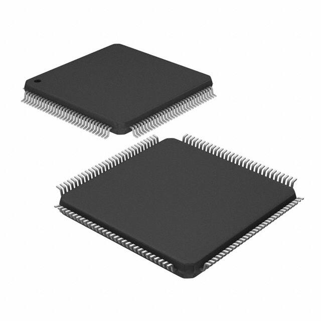
Available in 132-pin Plastic Quad Flatpack (PQF) or space-saving
120-pin Thin Quad Flatpack (PF)
Industrial temperature range (–40°°C to +85°°C) is available
Green parts available, see ordering information
FUNCTIONAL BLOCK DIAGRAM
PGB
Parity
Generation
ODD/
EVEN
Reset
Logic
MBF1
PEFB
Parity
Gen/Check
Mail 1
Register
Input
Register
RST
Port-A
Control
Logic
RAM
ARRAY
64 x 36
Output
Register
CLKA
CSA
W/RA
ENA
MBA
36
A0 - A35
Write
Pointer
FF
AF
Read
Pointer
B0 - B35
EF
AE
Status Flag
Logic
FIFO
FS0
FS1
Programmable
Flag Offset
Registers
PGA
PEFA
MBF2
Parity
Gen/Check
Mail 2
Register
Port-B
Control
Logic
CLKB
CSB
W/RB
ENB
MBB
3024 drw 01
IDT and the IDT logo are registered trademarks of Integrated Device Technology, Inc. SyncBIFIFO is a trademark of Integrated Device Technology, Inc.
COMMERCIAL AND INDUSTRIAL TEMPERATURE RANGES
FEBRUARY 2009
1
© 2009 Integrated Device Technology, Inc. All rights reserved. Product specifications subject to change without notice.
DSC-3024/3
�COMMERCIAL AND INDUSTRIAL
TEMPERATURE RANGES
IDT723611
CMOS SyncFIFOTM 64 x 36
DESCRIPTION (CONTINUED)
Flag (EF) and Almost-Empty (AE) flag of the FIFO are two-stage synchronized
to the port clock that reads data from its array.
The IDT723611 is characterized for operation from 0°C to 70°C.
The Full Flag (FF) and Almost-Full (AF) flag of the FIFO are two-stage
synchronized to the port clock that writes data into its array (CLKA). The Empty
64 x 36
120
119
118
117
116
115
114
113
112
111
110
109
108
107
106
105
104
103
102
101
100
99
98
97
96
95
94
93
92
91
A24
A25
A26
VCC
A27
A28
A29
GND
A30
A31
A32
A33
A34
A35
GND
B35
B34
B33
B32
B31
B30
GND
B29
B28
B27
VCC
B26
B25
B24
B23
PIN CONFIGURATIONS
1
2
3
4
5
6
7
8
9
10
11
12
13
14
15
16
17
18
19
20
21
22
23
24
25
26
27
28
29
30
90
89
88
87
86
85
84
83
82
81
80
79
78
77
76
75
74
73
72
71
70
69
68
67
66
65
64
63
62
61
B22
B21
GND
B20
B19
B18
B17
B16
B15
B14
B13
B12
B11
B10
GND
B9
B8
B7
VCC
B6
B5
B4
B3
GND
B2
B1
B0
EF
AE
NC
AF
FF
CSA
ENA
CLKA
W/RA
VCC
PGA
PEFA
MBF2
MBA
FS1
FS0
ODD/EVEN
RST
GND
NC
NC
NC
NC
MBB
MBF1
PEFB
PGB
VCC
W/RB
CLKB
ENB
CSB
NC
31
32
33
34
35
36
37
38
39
40
41
42
43
44
45
46
47
48
49
50
51
52
53
54
55
56
57
58
59
60
A23
A22
A21
GND
A20
A19
A18
A17
A16
A15
A14
A13
A12
A11
A10
GND
A9
A8
A7
VCC
A6
A5
A4
A3
GND
A2
A1
A0
NC
NC
3024 drw 02
NOTE:
1. Pin 1 identifier in corner.
2. NC = No internal connection
TQFP (PN120-1, order code: PF)
TOP VIEW
2
FEBRUARY 13, 2009
�COMMERCIAL AND INDUSTRIAL
TEMPERATURE RANGES
IDT723611
CMOS SyncFIFOTM 64 x 36
116
115
114
113
112
111
110
109
108
107
106
105
104
103
102
101
100
99
98
97
96
95
94
93
92
91
90
89
88
87
86
85
84
GND
AE
EF
B0
B1
B2
GND
B3
B4
B5
B6
VCC
B7
B8
B9
GND
B10
B11
VCC
B12
B13
B14
GND
B15
B16
B17
B18
B19
B20
GND
B21
B22
B23
51
52
53
54
55
56
57
58
59
60
61
62
63
64
65
66
67
68
69
70
71
72
73
74
75
76
77
78
79
80
81
82
83
18
19
20
21
22
23
24
25
26
27
28
29
30
31
32
33
34
35
36
37
38
39
40
41
42
43
44
45
46
47
48
49
50
VCC
A24
A25
A26
GND
A27
A28
A29
VCC
A30
A31
A32
GND
A33
A34
A35
GND
B35
B34
B33
GND
B32
B31
B30
VCC
B29
B28
B27
GND
B26
B25
B24
VCC
GND
NC
NC
A0
A1
A2
GND
A3
A4
A5
A6
VCC
A7
A8
A9
GND
A10
A11
VCC
A12
A13
A14
GND
A15
A16
A17
A18
A19
A20
GND
A21
A22
A23
17
16
15
14
13
12
11
10
9
8
7
6
5
4
3
2
1
132
131
130
129
128
127
126
125
124
123
122
121
120
119
118
117
AF
FF
CSA
ENA
CLKA
W/RA
VCC
PGA
PEFA
GND
MBF2
MBA
FS1
FS0
ODD/EVEN
RST
GND
NC
NC
NC
NC
MBB
MBF1
GND
PEFB
PGB
VCC
W/RB
CLKB
ENB
CSB
NC
NC
PIN CONFIGURATIONS (CONTINUED)
3024 drw 03
NOTES:
1. Electrical pin 1 in center of beveled edge.
2. NC = No internal connection.
PQFP (PQ132-1, order code: PQF)
TOP VIEW
3
FEBRUARY 13, 2009
�COMMERCIAL AND INDUSTRIAL
TEMPERATURE RANGES
IDT723611
CMOS SyncFIFOTM 64 x 36
PIN DESCRIPTION
Symbol
A0-A35
AE
Name
Port-A Data
64 x 36
Almost-Empty Flag
I/O
I/O
O
AF
Almost-Full Flag
O
B0-B35
CLKA
Port-B Data.
Port-A Clock
I/O
I
CLKB
Port-B Clock
I
CSA
Port-A Chip Select
I
CSB
Port-B Chip Select
I
EF
Empty Flag
O
ENA
ENB
FF
Port-A Enable
Port-B Enable
Full Flag
I
I
O
FS1, FS0
Flag-Offset Selects
I
MBA
MBB
Port-A Mailbox Select
Port-B Mailbox Select
I
I
MBF1
Mail1 Register Flag
O
MBF2
Mail2 Register Flag
O
ODD/
EVEN
Odd/Even Parity
Select
I
PEFA
Port-A Parity Error
Flag
O
(Port A)
PEFB
Port-B Parity Error
Flag
O
Description
36-bit bidirectional data port for side A.
Programmable Almost-Empty flag synchronized to CLKB. It is LOW when the number of words in the
FIFO is less than or equal to the value in the offset register, X.
Programmable Almost-Full flag synchronized to CLKA. It is LOW when the number of emptylocations
in the FIFO is less than or equal to the value in the Offset register, X.
36-bit bidirectional data port for side B.
CLKA is a continuous clock that synchronizes all data transfers through port-A and can be asynchronous or coincident to CLKB. FF and AF are synchronized to the LOW-to-HIGH transition of CLKA.
CLKB is a continuous clock that synchronizes all data transfers through port-B and can be asynchronous or coincident to CLKA. EF and AE are synchronized to the LOW-to-HIGH transition of CLKB.
CSA must be LOW to enable a LOW-to-HIGH transition of CLKA to read or write data on port-A. The
A0-A35 outputs are in the high-impedance state when CSA is HIGH.
CSB must be LOW to enable a LOW-to-HIGH transition of CLKB to read or write data on port-B. The
B0-B35 outputs are in the high-impedance state when CSB is HIGH.
EF is synchronized to the LOW-to-HIGH transition of CLKB. When EF is LOW, the FIFO is empty, and
reads from its memory are disabled. Data can be read from the FIFO to its output register when EF is
HIGH. EF is forced LOW when the device is reset and is set HIGH by the second LOW-to-HIGH
transition of CLKB after data is loaded into empty FIFO memory.
ENA must be HIGH to enable a LOW-to-HIGH transition of CLKA to read or write data on port-A.
ENB must be HIGH to enable a LOW-to-HIGH transition of CLKB to read or write data on port-B.
FF is synchronized to the LOW-to-HIGH/ transition of CLKA. When FF is LOW, the FIFO is full, and
writes to its memory are disabled. FF is forced LOW when the device is reset and is set HIGH by the
second LOW-to-HIGH transition of CLKA after reset.
The LOW-to-HIGH transition of RST latches the values of FS0 and FS1, which loads one of four
preset values into the Almost-Full and Almost-Empty Offset register (X).
A HIGH level on MBA chooses a mailbox register for a port-A read or write operation.
A HIGH level on MBB chooses a mailbox register for a port-B read or write operation. When the
B0-B35 outputs are active, a HIGH level on MBB selects data from the mail1 register for output, and a
LOW level selects the FIFO output register data for output.
MBF1 is set LOW by a LOW-to-HIGH transition of CLKA that writes data to the mail1 register. Writes to
the mail1 register are inhibited while MBF1 is set LOW. MBF1 is set HIGH by a LOW-to-HIGH
transition of CLKB when a port-B read is selected and MBB is HIGH. MBF1 is set HIGH when the
device is reset.
MBF2 is set LOW by a LOW-to-HIGH transition of CLKB that writes data to the mail2 register. Writes to
the mail2 register are inhibited while MBF2 is LOW. MBF2 is set HIGH by a LOW-to-HIGH transition of
CLKA when a port-A read is selected and MBA is HIGH. MBF2 is set HIGH when the device is reset.
Odd parity is checked on each port when ODD/EVEN is HIGH, and even parity is checked when
ODD/EVEN is LOW. ODD/EVEN also selects the type of parity generated for each port if parity
generation is enabled for a read operation.
When any byte applied to terminals A0-A35 fails parity, PEFA is LOW. Bytes are organized as
A0-A8, A9-A17, A18-A26, and A27-A35, with the most significant bit of each byte serving as the parity
bit. The type of parity checked is determined by the state of the ODD/EVEN input. The parity trees
used to check the A0-A35 inputs are shared by the mail2 register to generate parity if parity generation is selected by PGA. Therefore, if a mail2 read with parity generation is setup by having CSA
LOW, ENA HIGH, W/RA LOW, MBA HIGH, and PGA HIGH, the PEFA flag is forced HIGH regardless
of the state of A0-A35 inputs.
When any byte applied to terminals B0-B35 fails parity, PEFB is LOW. Bytes are organized as
(Port B) B0-B8, B9-B17, B18-B26, B27-B35, with the most significant bit of each byte serving as the
parity bit. The type of parity checked is determined by the state of the ODD/EVEN input. The parity
trees used to check the B0-B35 inputs are shared by the mail1 register to generate parity if parity
generation is selected by PGB. Therefore, if a mail1 read with parity generation is setup by having
CSB LOW, ENB HIGH, W/RB LOW, MBB HIGH, and PGB HIGH, the PEFB flag is forced HIGH
regardless of the state of the B0-B35 inputs
4
FEBRUARY 13, 2009
�COMMERCIAL AND INDUSTRIAL
TEMPERATURE RANGES
IDT723611
CMOS SyncFIFOTM 64 x 36
PIN DESCRIPTION (Continued)
Symbol
PGA
Name
Port-A Parity
Generation
PGB
Port-B Parity
Generation
RST
Reset
W/RA
Port-A Write/Read
Select
Port-B Write/Read
Select
W/RB
I/O
Description
I Parity is generated for mail2 register reads from port A when PGA is HIGH. The type of parity generated
is selected by the state of the ODD/EVEN input. Bytes are organized as A0-A8, A9-A17, A18-A26, and
A27-A35. The generated parity bits are output in the most significant bit of each byte.
I Parity is generated for data reads from port B when PGB is HIGH. The type of parity generated is selected
by the state of the ODD/EVEN input. Bytes are organized as B0-B8, B9-B17, B18-B26, and B27-B35.
The generated parity bits are output in the most significant bit of each byte.
I To reset the device, four LOW-to-HIGH transitions of CLKA and four LOW-to-HIGH transitions of CLKB
must occur while RST is LOW. This sets the AF, MBF1, and MBF2 flags HIGH and the EF, AE, and FF flags
LOW. The LOW-to-HIGH transition of RST latches the status of the FS1 and FS0 inputs to select AlmostFull and Almost-Empty flag offset.
I
A HIGH selects a write operation and a LOW selects a read operation on port A for a LOW-to-HIGH
transition of CLKA. The A0-A35 outputs are in the high-impedance state when W/RA isHIGH.
I A HIGH selects a write operation and a LOW selects a read operation on port B for a LOW-to-HIGH
transition of CLKB. The B0-B35 outputs are in the high-impedance state when W/RB is HIGH.
5
FEBRUARY 13, 2009
�COMMERCIAL AND INDUSTRIAL
TEMPERATURE RANGES
IDT723611
CMOS SyncFIFOTM 64 x 36
ABSOLUTE MAXIMUM RATINGS OVER OPERATING FREE-AIR
TEMPERATURE RANGE (Unless otherwise noted)(1)
Symbol
VCC
Rating
Commercial
Unit
Supply64
Voltage
x 36Range
Input Voltage Range
–0.5 to 7
V
VI(2)
–0.5 to VCC+0.5
V
VO(2)
Output Voltage Range
–0.5 to VCC+0.5
V
IIK
Input Clamp Current, (VI < 0 or VI > VCC)
±20
mA
IOK
Output Clamp Current, (VO = < 0 or VO > VCC)
±50
mA
IOUT
Continuous Output Current, (VO = 0 to VCC)
±50
mA
ICC
Continuous Current Through VCC or GND
±500
mA
TSTG
Storage Temperature Range
–65 to 150
°C
NOTES:
1. Stresses beyond those listed under "Absolute Maximum Ratings" may cause permanent damage to the device. These are stress ratings only and functional
operation of the device at these or any other conditions beyond those indicated under "Recommended Operating Conditions" is not implied. Exposure to absolutemaximum-rated conditions for extended periods may affect device reliability.
2. The input and output voltage ratings may be exceeded provided the input and output current ratings are observed.
RECOMMENDED OPERATING
CONDITIONS
Symbol
Parameter
VCC
Supply Voltage
VIH
High-Level Input Voltage
VIL
Low-Level Input Voltage
Min.
Max.
Unit
4.5
5.5
V
2
—
V
—
0.8
V
mA
IOH
High-Level Output Current
—
–4
IOL
Low-Level Output Current
—
8
mA
TA
Operating Free-Air Temperature
0
70
°C
ELECTRICAL CHARACTERISTICS OVER RECOMMENDED OPERATING
FREE-AIR TEMPERATURE RANGE (Unless otherwise noted)
IDT723611
Commercial & Industrial(1)
tA = 15, 20 ns
Parameter
Test Conditions
Min.
Typ.
(2)
Max.
Unit
VOH
VCC = 4.5V,
IOH = –4 mA
2.4
—
—
V
VOL
VCC = 4.5V,
IOL = 8 mA
—
—
0.5
V
ILI
VCC = 5.5V,
VI = VCC or 0
—
—
±50
µA
ILO
VCC = 5.5V,
VO = VCC or 0
—
—
±50
µA
ICC
VCC = 5.5V,
IO = 0 mA,
—
—
—
—
—
—
60
130
60
mA
CIN
VI = 0,
f = 1 MHz
—
4
—
pF
COUT
VO = 0,
f = 1 MHZ
—
8
—
pF
(3)
VI = VCC or GND
Outputs HIGH
Outputs LOW
Outputs Disabled
NOTES:
1. Industrial temperature range product for 20ns speed grade is available as a standard device. All other speed grades are available by special order.
2. All typical values are at VCC = 5V, TA = 25°C.
3. For additional ICC information, see the following page.
6
FEBRUARY 13, 2009
�COMMERCIAL AND INDUSTRIAL
TEMPERATURE RANGES
IDT723611
CMOS SyncFIFOTM 64 x 36
400
VCC = 5.5V
350
fdata = 1/2 fS
TA = 25°C
CL = 0 pF
300
mA
VCC = 5.0V
Icc(f)
Supply Current
250
VCC = 4.5V
200
150
100
50
0
0
10
20
30
40
50
60
fclock ⎯ Clock Frequency ⎯ MHz
70
80
3024 drw 04
Figure 1. Typical Characteristics: Supply Current vs Clock Frequency
CALCULATING POWER DISSIPATION
The ICC(f) data for the graph was taken while simultaneously reading and writing the FIFO on the IDT723611 with CLKA and CLKB operating at
frequency fS. All data inputs and data outputs change state during each clock cycle to consume the highest supply current. Data outputs were disconnected to normalize the graph to a zero-capacitance load. Once the capacitance load per data-output channel is known, the power dissipation can be
calculated with the equation below.
With ICC(f) taken from Figure 1, the maximum power dissipation (PT) of the IDT723611 may be calculated by:
PT = VCC x ICC(f) + Σ(CL x VOH - VOL)2 X fO)
where:
CL
fO
=
=
output capacitance load
switching frequency of an output
VOH
=
output high-level voltage
VOL
=
output low-level voltage
When no read or writes are occurring on this device, the power dissipated by a single clock (CLKA or CLKB) input running at frequency fS is
calculated by:
PT = VCC x fS x 0.290 mA/MHz
7
FEBRUARY 13, 2009
�COMMERCIAL AND INDUSTRIAL
TEMPERATURE RANGES
IDT723611
CMOS SyncFIFOTM 64 x 36
TIMING REQUIREMENTS OVER RECOMMENDED RANGES OF SUPPLY
VOLTAGE AND OPERATING FREE-AIR TEMPERATURES
(Commercial: VCC = 5.0V ±10%, TA = 0°C to +70°C; Industrial; VCC = 5.0V ± 10%,TA = 40°C to +85°C)
64 x 36
Symbol
fS
tCLK
tCLKH
tCLKL
tDS
tENS1
tENS2
tENS3
tPGS
tRSTS
Parameter
Clock Frequency, CLKA or CLKB
Clock Cycle Time, CLKA or CLKB
Pulse Duration, CLKA or CLKB HIGH
Pulse Duration, CLKA or CLKB LOW
Setup Time, A0-A35 before CLKA↑ and B0-B35 before CLKB↑
CSA, W/RA, before CLKA↑; CSB, W/RB before CLKB↑
ENA before CLKA↑; ENB before CLKB↑
MBA before CLKA↑; ENB before CLKB↑
Setup Time, ODD/EVEN and PGB before CLKB↑(1)
Setup Time, RST LOW before CLKA↑ or CLKB↑(2)
tFSS
tDH
tENH1
tENH2
tENH3
tPGH
tRSTH
tFSH
tSKEW1(4)
tSKEW2(4)
Setup Time, FS0 and FS1 before RST HIGH
Hold Time, A0-A35 after CLKA↑ and B0-B35 after CLKB↑
CSA, W/RA after CLKA↑; CSB, W/RB after CLKB↑
ENA after CLKA↑; ENB after CLKB↑
MBA after CLKA↑; MBB after CLKB↑
Hold TIme, ODD/EVEN and PGB after CLKB↑(2)
Hold Time, RST LOW after CLKA↑ or CLKB↑(3)
Hold Time, FS0 and FS1 after RST HIGH
Skew Time, between CLKA↑ and CLKB↑ for EF, FF
Skew Time, between CLKA↑ and CLKB↑ for AE, AF
Commercial
Com'l & Ind'l(1)
IDT723611L15
Min.
Max.
–
66.7
15
–
6
–
6
–
4
–
6
–
4
–
4
–
4
–
5
–
IDT723611L20
Min.
Max.
–
50
20
–
8
–
8
–
5
–
6
–
5
–
5
–
5
–
6
–
5
1
1
1
1
0
6
4
8
14
–
–
–
–
–
–
–
–
–
–
6
1
1
1
1
0
6
4
8
16
–
–
–
–
–
–
–
–
–
–
Unit
MHz
MHz
ns
ns
ns
ns
ns
ns
ns
ns
ns
ns
ns
ns
ns
ns
ns
ns
ns
ns
NOTES:
1. Industrial Temperature Range product for 20ns speed grade is available as a standard device. All other speed grades are available by special order.
2. Only applies for a rising edge of CLKB that does a FIFO read.
3. Requirement to count the clock edge as one of at least four needed to reset a FIFO.
4. Skew time is not a timing constraint for proper device operation and is only included to illustrate the timing relationship between CLKA cycle and CLKB cycle.
8
FEBRUARY 13, 2009
�COMMERCIAL AND INDUSTRIAL
TEMPERATURE RANGES
IDT723611
CMOS SyncFIFOTM 64 x 36
SWITCHING CHARACTERISTICS OVER RECOMMENDED RANGES OF SUPPLY
VOLTAGE AND OPERATING FREE-AIR TEMPERATURE, CL = 30 PF
(Commercial: VCC = 5.0V ±10%, TA = 0°C to +70°C; Industrial; VCC = 5.0V ± 10%,TA = 40°C to +85°C)
Symbol
fS
tA
tWFF
tREF
tPAE
tPAF
tPMF
tPMR
tMDV
tPDPE
tPOPE
tPOPB(4)
tPEPE
tPEPB(4)
tRSF
tEN
tDIS
Parameter
Clock Frequency, CLKA or CLKB
Access Time, CLKB↑ to B0-B35
Propagation Delay Time, CLKA↑ to FF
Propagation Delay Time, CLKB↑ to EF
Propagation Delay Time, CLKB↑ to AE
Propagation Delay Time, CLKA↑ to AF
Propagation Delay Time, CLKA↑ to MBF1 LOW or MBF2 HIGH and CLKB↑
to MBF2 LOW or MBF1 HIGH
Propagation Delay Time, CLKA↑ to B0-B35(2) and CLKB↑ to A0-A35(3)
Propagation Delay Time, MBB to B0-B35 Valid
Propagation Delay Time, A0-A35 Valid to PEFA Valid; B0-B35 Valid to
PEFB Valid
Propagation Delay Time, ODD/EVEN to PEFA and PEFB
Propagation Delay Time, ODD/EVEN to Parity Bits (A8, A17, A26, A35) and
(B8, B17, B26, B35)
Propagation Delay Time, CSA, ENA, W/RA, MBA, or PGA to PEFA; CSB,
ENB, W/RB, MBB, or PGB to PEFB
Propagation Delay Time, CSA, ENA W/RA, MBA, or PGA to Parity Bits (A8, A17,
A26, A35); CSB, ENB, W/RB, MBB, or PGB to ParityBits (B8, B17, B26, B35)
Propagation Delay Time, RST to AE LOW and (AF, MBF1, MBF2) HIGH
Enable Time, CSA and W/RA LOW to A0-A35 Active and CSB LOW and W/RB
HIGH to B0-B35 Active
Disable Time, CSA or W/RA HIGH to A0-A35 at high impedance and CSB HIGH
or W/RB LOW to B0-B35 at high impedance
Commercial
Com'l & Ind'l(1)
IDT723611L15
Min.
Max.
–
66.7
2
10
2
10
2
10
2
10
2
10
1
9
IDT723611L20
Min.
Max.
–
50
2
12
2
12
2
12
2
12
2
12
1
12
Unit
MHz
ns
ns
ns
ns
ns
ns
3
1
12
11
3
1
14
11.5
ns
ns
3
12
3
13
ns
3
2
11
12
3
2
12
13
ns
ns
1
12
1
13
ns
3
14
3
15
ns
1
2
15
10
1
2
20
12
ns
ns
1
9
1
10
ns
NOTES:
1. Industrial temperature range product for 20ns speed grade is available as a standard device. All other speed grades are available by special order.
2. Writing data to the mail1 register when the B0-B35 outputs are active and MBB is HIGH.
3 Writing data to the mail2 register when the A0-A35 outputs are active and MBA is HIGH.
4. Only applies when reading data from a mail register.
9
FEBRUARY 13, 2009
�COMMERCIAL AND INDUSTRIAL
TEMPERATURE RANGES
IDT723611
CMOS SyncFIFOTM 64 x 36
SIGNAL DESCRIPTION
RESET ( RST )
The IDT723611 is reset by taking the Reset (RST) input LOW for at least
four port-A clock (CLKA)
four port-B clock (CLKB) LOW-to-HIGH transi64and
x 36
tions. The reset input can switch asynchronously to the clocks. A device reset
initializes the internal read and write pointers of the FIFO and forces the Full Flag
(FF) LOW, the Empty Flag (EF) LOW, the Almost-Empty flag (AE) LOW, and the
Almost-Full flag (AF) HIGH. A reset also forces the Mailbox Flags (MBF1, MBF2)
HIGH. After a reset, FF is set HIGH after two LOW-to-HIGH transitions of CLKA.
The device must be reset after power up before data is written to its memory.
A LOW-to-HIGH transition on the RST input loads the Almost-Full and AlmostEmpty Offset register (X) with the value selected by the Flag Select (FS0, FS1)
inputs. The values that can be loaded into the register are shown in Table 1.
TABLE 1 — FLAG PROGRAMMING
Almost-Full and
Almost-Empty Flag
Offset Register (X)
FS1
FS0
RST
16
H
H
↑
12
H
L
↑
8
L
H
↑
4
L
L
↑
FIFO WRITE/READ OPERATION
The state of the port-A data (A0-A35) outputs is controlled by the port-A Chip
Select (CSA) and the port-A Write/Read select (W/RA). The A0-A35 outputs
are in the high-impedance state when either CSA or W/RA is HIGH. The A0A35 outputs are active when both CSA and W/RA are LOW. Data is loaded into
the FIFO from the A0-A35 inputs on a LOW-to-HIGH transition of CLKA when
CSA is LOW, W/RA is HIGH, ENA is HIGH, MBA is LOW, and FF is HIGH (see
Table 2).
The port-B control signals are identical to those of port A. The state of the
port-B data (B0-B35) outputs is controlled by the port-B Chip Select (CSB) and
the port-B Write/Read select (W/RB). The B0-B35 outputs are in the highimpedance state when either CSB or W/RB is HIGH. The B0-B35 outputs are
active when both CSB and W/RB are LOW. Data is read from the FIFO to the
B0-B35 outputs by a LOW-to-HIGH transition of CLKB when CSB is LOW, W/RB
is LOW, ENB is HIGH, MBB is LOW, and EF is HIGH (see Table 3).
The setup and hold-time constraints to the port clocks for the port Chip
Selects (CSA, CSB) and Write/Read selects (W/RA, W/RB) are only for enabling
write and read operations and are not related to HIGH-impedance control of
the data outputs. If a port enable is LOW during a clock cycle, the port’s Chip
Select and Write/Read select can change states during the setup and hold-time
window of the cycle.
SYNCHRONIZED FIFO FLAGS
Each FIFO flag is synchronized to its port clock through two flip-flop stages.
This is done to improve the flags’ reliability by reducing the probability of
mestastable events on their outputs when CLKA and CLKB operate asynchronously to one another. FF and AF are synchronized to CLKA. EF and AE are
synchronized to CLKB. Table 4 shows the relationship to the flags to the FIFO.
TABLE 2 — PORT-A ENABLE FUNCTION TABLE
CSA
W/RA
ENA
MBA
CLKA
A0-A35 Outputs
Port Functions
H
X
X
X
X
In High-Impedance State
None
L
H
L
X
X
In High-Impedance State
None
L
H
H
L
↑
In High-Impedance State
FIFO Write
L
H
H
H
↑
In High-Impedance State
Mail1 Write
L
L
L
L
X
Active, Mail2 Register
None
L
L
H
L
↑
Active, Mail2 Register
None
L
L
L
H
X
Active, Mail2 Register
None
L
L
H
H
↑
Active, Mail2 Register
Mail2 Read (set MBF2 HIGH)
TABLE 3 — PORT-B ENABLE FUNCTION TABLE
CSB
W/RB
ENB
MBB
CLKB
B0-B35 Outputs
Port Functions
H
X
X
X
X
In High-Impedance State
None
L
H
L
X
X
In High-Impedance State
None
L
H
H
L
↑
In High-Impedance State
None
L
H
H
H
↑
In High-Impedance State
Mail2 Write
L
L
L
L
X
Active, FIFO Output Register
None
L
L
H
L
↑
Active, FIFO Output Register
FIFO Read
L
L
L
H
X
Active, Mail1 Register
None
L
L
H
H
↑
Active, Mail1 Register
Mail1 Read (set MBF1 HIGH)
10
FEBRUARY 13, 2009
�COMMERCIAL AND INDUSTRIAL
TEMPERATURE RANGES
IDT723611
CMOS SyncFIFOTM 64 x 36
EMPTY FLAG ( EF )
The FIFO Empty Flag is synchronized to the port clock that reads data from
its array (CLKB). When the EF is HIGH, new data can be read to the FIFO output
register. When the EF is LOW, the FIFO is empty and attempted FIFO reads
are ignored.
The FIFO read pointer is incremented each time a new word is clocked
to its output register. The state machine that controls an EF monitors a write
pointer and read pointer comparator that indicates when the FIFO SRAM
status is empty, empty+1, or empty+2. A word written to the FIFO can be read
to the FIFO output register in a minimum of three port-B clock (CLKB) cycles.
Therefore, an EF is LOW if a word in memory is the next data to be sent to the
FIFO output register and two CLKB cycles have not elapsed since the time the
word was written. The EF of the FIFO is set HIGH by the second LOW-to-HIGH
transition of CLKB, and the new data word can be read to the FIFO output register
in the following cycle.
A LOW-to-HIGH transition on CLKB begins the first synchronized cycle of
a write if the clock transition occurs at time tSKEW1 or greater after the write.
Otherwise, the subsequent CLKB cycle can be the first synchronization cycle
(see Figure 5).
FULL FLAG ( FF )
The FIFO Full Flag is synchronized to the port clock that writes data to
its array (CLKA). When the FF is HIGH, an SRAM location is free to receive
new data. No memory locations are free when the FF is LOW and attempted
writes to the FIFO are ignored.
Each time a word is written to the FIFO, its write pointer is incremented. The
state machine that controls the FF monitors a write pointer and read pointer
comparator that indicates when the FIFO SRAM status is full, full-1, or full-2. From
the time a word is read from the FIFO, its previous memory location is ready
to be written in a minimum of three port-A clock cycles. Therefore, a FF is LOW
if less than two CLKA cycles have elapsed since the next memory write location
has been read. The second LOW-to-HIGH transition on CLKA after the read
sets the FF HIGH and data can be written in the following clock cycle.
A LOW-to-HIGH transition on CLKA begins the first synchronization cycle
of a read if the clock transition occurs at time tSKEW1 or greater after the read.
Otherwise, the subsequent clock cycle can be the first synchronization cycle (see
Figure 6).
ALMOST-EMPTY FLAG ( AE )
The FIFO Almost-Empty flag is synchronized to the port clock that reads data
from its array (CLKB). The state machine that controls the AE flag monitors a
TABLE 4 — FIFO FLAG OPERATION
Number of Words
in the FIFO
Synchronized
to CLKB
Synchronized
to CLKA
EF
AE
AF
FF
0
L
L
H
H
1 to X
H
L
H
H
(X+1) to [64-(X+1)]
H
H
H
H
(64-X) to 63
H
H
L
H
64
H
H
L
L
write pointer and read pointer comparator that indicates when the FIFO SRAM
status is almost-empty, almost-empty+1, or almost-empty+2. The almost-empty
state is defined by the value of the Almost-Full and Almost-Empty Offset register
(X). This register is loaded with one of four preset values during a device reset
(see reset above). The AE flag is LOW when the FIFO contains X or less words
in memory and is HIGH when the FIFO contains (X+1) or more words.
Two LOW-to-HIGH transitions on the port-B clock (CLKB) are required
after a FIFO write for the AE flag to reflect the new level of fill. Therefore, the
AE flag of a FIFO containing (X+1) or more words remains LOW if two CLKB
cycles have not elapsed since the write that filled the memory to the (X+1) level.
The AE flag is set HIGH by the second CLKB LOW-to-HIGH transition after the
FIFO write that fills memory to the (X+1) level. A LOW-to-HIGH transition on
CLKB begins the first synchronization cycle if it occurs at time tSKEW2 or greater
after the write that fills the FIFO to (X+1) words. Otherwise, the subsequent CLKB
cycle can be the first synchronization cycle (see Figure 7).
ALMOST-FULL FLAG ( AF )
The FIFO Almost-Full flag is synchronized to the port clock that writes
data to its array (CLKA). The state machine that controls an AF flag monitors
a write pointer and read pointer comparator that indicates when the FIFO SRAM
status is almost-full, almost- full-1, or almost-full-2. The almost-full state is defined
by the value of the Almost-Full and Almost-Empty Offset register (X). This register
is loaded with one of four preset values during a device reset (see reset above).
The AF flag is LOW when the FIFO contains (64-X) or more words in memory
and is HIGH when the FIFO contains [64-(X+1)] or less words.
Two LOW-to-HIGH transitions on the port-A clock (CLKA) are required
after a FIFO read for the AF flag to reflect the new level of fill. Therefore, the
AF flag of a FIFO containing [64-(X+1)] or less words remains LOW if two CLKA
cycles have not elapsed since the read that reduced the number of words in
memory to [64-(X+1)]. The AF flag is set HIGH by the second CLKA LOW-toHIGH transition after the FIFO read that reduces the number of words in memory
to [64-(X+1)]. A LOW-to-HIGH transition on CLKA begins the first synchronization cycle if it occurs at time tSKEW2 or greater after the read that reduces the
number of words in memory to [64-(X+1)]. Otherwise, the subsequent CLKA
cycle can be the first synchronization cycle (see Figure 8).
MAILBOX REGISTERS
Two 36-bit bypass registers are on the IDT723611 to pass command and
control information between port A and port B. The Mailbox select (MBA, MBB)
inputs choose between a mail register and a FIFO for a port data transfer
operation. A LOW-to-HIGH transition on CLKA writes A0-A35 data to the mail1
register when port-A write is selected by CSA, W/RA, and ENA with MBA HIGH.
A LOW-to-HIGH transition on CLKB writes B0-B35 data to the mail2 register
when port-B write is selected by CSB, W/RB, and ENB with MBB HIGH. Writing
data to a mail register sets its corresponding flag (MBF1 or MBF2) LOW.
Attempted writes to a mail register are ignored while its mail flag is LOW.
When the port-B data (B0-B35) outputs are active, the data on the bus
comes from the FIFO output register when the port-B Mailbox select (MBB)
input is LOW and from the mail1 register when MBB is HIGH. Mail2 data is always
present on the port-A data (A0-A35) outputs when they are active. The Mail1
Register Flag (MBF1) is set HIGH by a LOW-to-HIGH transition on CLKB when
a port-B read is selected by CSB, W/RB, and ENB with MBB HIGH. The Mail2
Register Flag (MBF2) is set HIGH by a LOW-to-HIGH transition on CLKA when
a port-A read is selected by CSA, W/RA, and ENA with MBA HIGH. The data
in a mail register remains intact after it is read and changes only when new data
is written to the register.
NOTE:
1. X is the value in the Almost-Empty flag and Almost-Full flag register.
11
FEBRUARY 13, 2009
�COMMERCIAL AND INDUSTRIAL
TEMPERATURE RANGES
IDT723611
CMOS SyncFIFOTM 64 x 36
PARITY CHECKING
The port-A (A0-A35) inputs and port-B (B0-B35) inputs each have four
parity trees to check the parity of incoming (or outgoing) data. A parity failure
on one or more bytes of the input bus is reported by a LOW level on the port
Parity Error Flag (PEFA,
64PEFB).
x 36 Odd or even parity checking can be selected,
and the Parity Error Flags can be ignored if this feature is not desired.
Parity status is checked on each input bus according to the level of the Odd/
Even parity (ODD/EVEN) select input. A parity error on one or more bytes of
a port is reported by a LOW level on the corresponding port Parity Error Flag
(PEFA, PEFB) output. Port-A bytes are arranged as A0-A8, A9-A17, A18-A26,
and A27-A35, and port-B bytes are arranged as B0-B8, B9-B17, B18-B26,
and B27-B35. When Odd/Even parity is selected, a port Parity Error Flag
(PEFA, PEFB) is LOW if any byte on the port has an odd/even number of LOW
levels applied to its bits.
The four parity trees used to check the A0-A35 inputs are shared by the
mail2 register when parity generation is selected for port-A reads (PGA=HIGH).
When port-A read from the mail2 register with parity generation is selected with
CSA LOW, ENA HIGH, W/RA LOW, MBA HIGH, and PGA HIGH, the port-A
Parity Error Flag (PEFA) is held HIGH regardless of the levels applied to the
A0-A35 inputs. Likewise, the parity trees used to check the B0-B35 inputs are
shared by the mail1 register when parity generation is selected for port-B reads
(PGB=HIGH). When a port-B read from the mail1 register with parity generation
is selected with CSB LOW, ENB HIGH, W/RB LOW, MBB HIGH, and PGB HIGH,
the port-B Parity Error Flag (PEFB) is held HIGH regardless of the levels applied
to the B0-B35 inputs.
PARITY GENERATION
A HIGH level on the port-A Parity Generate select (PGA) or port-B Parity
Generate select (PGB) enables the IDT723611 to generate parity bits for port
reads from a FIFO or mailbox register. Port-A bytes are arranged as A0-A8,
A9-A17, A18-A26, and A27-A35, with the most significant bit of each byte used
as the parity bit. Port-B bytes are arranged as B0-B8, B9-B17, B18-B26, and
B27-B35, with the most significant bit of each byte used as the parity bit. A write
to a FIFO or mail register stores the levels applied to all thirty-six inputs
regardless of the state of the Parity Generate select (PGA, PGB) inputs. When
data is read from a port with parity generation selected, the lower eight bits of
each byte are used to generate a parity bit according to the level on the ODD/
EVEN select. The generated parity bits are substituted for the levels originally
written to the most significant bits of each byte as the word is read to the data
outputs.
Parity bits for FIFO data are generated after the data is read from SRAM
and before the data is written to the output register. Therefore, the port-B Parity
Generate select (PGB) and ODD/EVEN have setup and hold time constraints
to the port-B clock (CLKB) for a rising edge of CLKB used to read a new word
to the FIFO output register.
The circuit used to generate parity for the mail1 data is shared by the
port-B bus (B0-B35) to check parity and the circuit used to generate parity
for the mail2 data is shared by the port-A bus (A0-A35) to check parity. The
shared parity trees of a port are used to generate parity bits for the data in
a mail register when the port Write/Read select (W/RA, W/RB) input is LOW, the
port Mail select (MBA, MBB) input is HIGH, Chip Select (CSA, CSB) is LOW,
Enable (ENA, ENB) is HIGH, and the port Parity Generate select (PGA, PGB)
is HIGH. Generating parity for mail register data does not change the contents
of the register.
CLKA
tRSTH
CLKB
tRSTS
tFSH
tFSS
RST
0,1
FS1,FS0
tWFF
tWFF
FF
tREF
EF
tPAE
AE
tPAF
AF
MBF1,
MBF2
tRSF
3024drw 05
Figure 2. Device Reset Loading the X Register with the Value of Eight
12
FEBRUARY 13, 2009
�COMMERCIAL AND INDUSTRIAL
TEMPERATURE RANGES
IDT723611
CMOS SyncFIFOTM 64 x 36
tCLK
tCLKH
tCLKL
CLKA
FF
tENS1
tENH1
CSA
tENS1
tENH1
tENS3
tENH3
tENS2
tENH2
W/RA
MBA
tENS2
tENH2
tENS2
tENH2
ENA
tDH
tDS
W1
A0 - A35
ODD/
EVEN
No Operation
W2
tPDPE
tPDPE
PEFA
Valid
Valid
3024 drw 06
Figure 3. FIFO Write Cycle Timing
tCLKH
tCLK
tCLKL
CLKB
EF HIGH
CSB
W/RB
tENS2
MBB
tENH2
tENS2
tENH2
tENH2
tENS2
ENB
No Operation
tMDV
tEN
B0 - B35
PGB,
ODD/
EVEN
tA
Previous Data
tPGH
tPGS
tDIS
tA
Word 1
tPGS
Word 2
tPGH
3024 drw 07
Figure 4. FIFO Read Cycle Timing
13
FEBRUARY 13, 2009
�COMMERCIAL AND INDUSTRIAL
TEMPERATURE RANGES
IDT723611
CMOS SyncFIFOTM 64 x 36
tCLK
tCLKH tCLKL
CLKA
CSA
LOW
64 x 36
WRA
HIGH tENS3
tENH3
tENS2
tENH2
MBA
ENA
FFA
HIGH
tDS
tDH
W1
A0 - A35
tSKEW1(1)
CLKB
tCLK
tCLKH tCLKL
1
2
tREF
EF
tREF
Empty FIFO
CSB
LOW
W/RB
LOW
MBB
LOW
tENS2
tENH2
ENB
tA
W1
B0 - B35
3024 drw 08
NOTE:
1. tSKEW1 is the minimum time between a rising CLKA edge and a rising CLKB edge for EF to transition HIGH in the next CLKB cycle. If the time between the rising CLKA edge and
rising CLKB edge is less than tSKEW1, then the transition of EF HIGH may occur one CLKB cycle later than shown.
Figure 5. EF Flag Timing and First Data Read when the FIFO is Empty
14
FEBRUARY 13, 2009
�COMMERCIAL AND INDUSTRIAL
TEMPERATURE RANGES
IDT723611
CMOS SyncFIFOTM 64 x 36
tCLKH
tCLK
tCLKL
CLKB
CSB
LOW
W/RB
LOW
MBB
LOW
tENS2
tENH2
ENB
EFB
B0 - B35
HIGH
tA
Previous Word in FIFO Output Register
Next Word From FIFO
tSKEW1(1)
tCLKH
tCLK
tCLKL
1
CLKA
2
tWFF
tWFF
FF
FIFO Full
CSA LOW
WRA
HIGH
tENS3
tENH3
tENS2
tENH2
MBA
ENA
tDS
tDH
A0 - A35
3024 drw 09
NOTE:
1. tSKEW1 is the minimum time between a rising CLKB edge and a rising CLKA edge for FF to transition HIGH in the next CLKA cycle. If the time between the rising CLKB edge
and rising CLKA edge is less than tSKEW1, then the transition of FF HIGH may occur one CLKA cycle later than shown.
Figure 6. FF Flag Timing and First Available Write when the FIFO is Full
CLKA
tENS2
tENH2
ENA
tSKEW2(1)
CLKB
1
2
tPAE
AE
X Word in FIFO
tPAE
(X+1) Words in FIFO
tENS2
tENH2
ENB
3024 drw 10
NOTES:
1. tSKEW2 is the minimum time between a rising CLKA edge and a rising CLKB edge for AE to transition HIGH in the next CLKB cycle. If the time between the rising CLKA edge
and rising CLKB edge is less than tSKEW2, then AE may transition HIGH one CLKB cycle later than shown.
2. FIFO write (CSA = L, W/RA = H, MBA = L), FIFO read (CSB = L, W/RB = L, MBB = L).
Figure 7. Timing for AE when the FIFO is Almost-Empty
15
FEBRUARY 13, 2009
�COMMERCIAL AND INDUSTRIAL
TEMPERATURE RANGES
IDT723611
CMOS SyncFIFOTM 64 x 36
tSKEW2(1)
tENS2
ENA
2
1
CLKA
tENH2
64 x 36
tPAF
AF
tPAF
(64-X) Words in FIFO
[64-(X+1)] Words in FIFO
CLKB
tENS2
tENH2
ENB
3024 drw 11
NOTES:
1. tSKEW2 is the minimum time between a rising CLKA edge and a rising CLKB edge for AF to transition HIGH in the next CLKA cycle. If the time between the rising CLKA edge
and rising CLKB edge is less than tSKEW2, then AF may transition HIGH one CLKB cycle later than shown.
2. FIFO write (CSA = L, W/RA = H, MBA = L), FIFO read (CSB = L, W/RB = L, MBB = L).
Figure 8. Timing for AF when the FIFO is Almost-Full
CLKA
tENS1
CSA
tENH1
tENS1
tENH1
tENS1
tENH1
tENS1
tENH1
W/RA
MBA
ENA
tDS
W1
A0 - A35
tDH
CLKB
tPMF
tPMF
MBF1
CSB
W/RB
MBB
tENS2
tENH2
ENB
tEN
B0 - B35
tMDV
FIFO Output Register
tPMR
tDIS
W1 (Remains valid in Mail1 Register after read)
3024 drw 12
NOTE:
1. Port-B parity generation off (PGB = L)
Figure 9. Timing for Mail1 Register and MBF1 Flag
16
FEBRUARY 13, 2009
�COMMERCIAL AND INDUSTRIAL
TEMPERATURE RANGES
IDT723611
CMOS SyncFIFOTM 64 x 36
CLKB
tENS1
tENH1
tENS1
tENH1
tENS1
tENH1
tENS1
tENH1
CSB
W/RB
MBB
ENB
tDS
W1
B0 - B35
tDH
CLKA
tPMF
tPMF
MBF2
CSA
W/RA
MBA
tENS2
tENH2
ENA
tEN
tPMR
tDIS
W1 (Remains valid in Mail2 Register after read)
A0 - A35
3024 drw 13
NOTE:
1. Port-A parity generation off (PGA = L)
Figure 10. Timing for Mail2 Register and MBF2 Flag
ODD/
EVEN
W/RA
MBA
PGA
Valid
tPEPE
tPOPE
tPOPE
PEFA
Valid
Valid
tPEPE
Valid
3024 drw 14
NOTE:
1. CSA = L and ENA = H.
Figure 11. ODD/EVEN, W/RA, MBA, and PGA to PEFA Timing
17
FEBRUARY 13, 2009
�COMMERCIAL AND INDUSTRIAL
TEMPERATURE RANGES
IDT723611
CMOS SyncFIFOTM 64 x 36
ODD/
EVEN
W/RB
MBB
64 x 36
PGB
tPOPE
PEFB
Valid
tPEPE
tPOPE
Valid
tPEPE
Valid
Valid
3024 drw 15
NOTE:
1. CSB = L and ENB = H.
Figure 12. ODD/EVEN, W/RB, MBB, and PGB to PEFB Timing
ODD/
EVEN
CSA
LOW
W/RA
MBA
PGA
tEN
A8, A17,
A26, A35
tPEPB
tPOPB
Generated Parity
Mail2 Data
tPEPB
Generated Parity
Mail2 Data
3024 drw 16
NOTE:
1. ENA = H.
Figure 13. Parity Generation Timing when reading from the Mail2 Register
ODD/
EVEN
CSB
LOW
W/RB
MBB
PGB
tEN
B8, B17,
B26, B35
tPEPB
tMDV
tPOPB
Generated Parity
tPEPB
Generated Parity
Mail1
Data
Mail1 Data
3024 drw 17
NOTE:
1. ENB = H.
Figure 14. Parity Generation Timing when reading from the Mail1 Register
18
FEBRUARY 13, 2009
�COMMERCIAL AND INDUSTRIAL
TEMPERATURE RANGES
IDT723611
CMOS SyncFIFOTM 64 x 36
PARAMETER MEASUREMENT INFORMATION
5V
1.1 kΩ
From Output
Under Test
30 pF
(1)
680Ω
PROPAGATION DELAY
LOAD CIRCUIT
3V
Timing
Input
1.5 V
GND
tS
th
GND
tW
3V
1.5 V
1.5 V
1.5 V
1.5 V
3V
Data,
Enable
Input
Low-Level
Input
GND
VOLTAGE WAVEFORMS
SETUP AND HOLD TIMES
1.5 V
1.5 V
GND
VOLTAGE WAVEFORMS
PULSE DURATIONS
3V
Output
Enable
1.5 V
tPLZ
1.5 V
GND
≈3 V
tPZL
Input
1.5 V
Low-Level
Output
VOL
tPZH
VOH
High-Level
Output
3V
High-Level
Input
1.5 V
tPHZ
≈ OV
VOLTAGE WAVEFORMS
ENABLE AND DISABLE TIMES
3V
1.5 V
1.5 V
tPD
tPD
GND
VOH
In-Phase
Output
1.5 V
1.5 V
VOLTAGE WAVEFORMS
PROPAGATION DELAY TIMES
VOL
3024 drw 18
NOTE:
1. Includes probe and jig capacitance.
Figure 16. Load Circuit and Voltage Waveforms
19
FEBRUARY 13, 2009
�ORDERING INFORMATION
XXXXXX
Device Type
X
Power
XX
Speed
X
Package
X
X
Process/
Temperature
Range
BLANK
I(1)
Commercial (0°C to +70°C)
Industrial (40°C to +85°C)
G
Green
PF
PQF
Thin Quad Flat Pack (TQFP, PN120-1)
Plastic Quad Flat Pack (PQFP, PQ132-1)
15
20
Commercial Only
Com'l & Ind'l
L
Low Power
723611
64 x 36 Synchronous FIFO
Clock Cycle Time (tCLK)
Speed in Nanoseconds
3024 drw 19
NOTES:
1. Industrial temperature range product for 20ns speed grade is avaiable as a standard device. All other speed grades are available by special order.
2. Green parts are available. For specific speeds and packages contact your sales office.
DATASHEET DOCUMENT HISTORY
03/05/2002
06/01/2005
02/13/2009
pgs. 1, 6, 8, 9 and 20.
pgs. 1,2,3 and 20.
pg. 20.
CORPORATE HEADQUARTERS
6024 Silver Creek Valley Road
San Jose, Ca 95138
for SALES:
800-345-7015 or 408-284-8200
fax: 408-284-2775
www.idt.com
20
for TECH SUPPORT:
408-360-1753
FIFOhelp@idt.com
�