2.5 VOLT HIGH-SPEED TeraSync™ DDR/SDR FIFO 40-BIT CONFIGURATION
16,384 x 40, 32,768 x 40,
65,536 x 40, 131,072 x 40
IDT72T4088, IDT72T4098
IDT72T40108, IDT72T40118
FEATURES
•
•
•
•
•
•
•
•
•
•
•
•
•
•
Choose among the following memory organizations:
IDT72T4088 ⎯ 16,384 x 40
IDT72T4098 ⎯ 32,768 x 40
IDT72T40108 ⎯ 65,536 x 40
IDT72T40118 ⎯ 131,072 x 40
Up to 250MHz operating frequency or 10Gbps throughput in SDR mode
Up to 110MHz operating frequency or 10Gbps throughput in DDR mode
Users selectable input port to output port data rates, 500Mb/s
Data Rate
-DDR to DDR
-DDR to SDR
-SDR to DDR
-SDR to SDR
User selectable HSTL or LVTTL I/Os
Read Enable & Read Clock Echo outputs aid high speed operation
2.5V LVTTL or 1.8V, 1.5V HSTL Port Selectable Input/Ouput voltage
3.3V Input tolerant
Mark & Retransmit, resets read pointer to user marked position
Write Chip Select (WCS) input enables/disables Write
Operations
Read Chip Select (RCS) synchronous to RCLK
Programmable Almost-Empty and Almost-Full flags, each flag
•
•
•
•
•
•
•
•
•
•
•
•
•
can default to one of four preselected offsets
Dedicated serial clock input for serial programming of flag offsets
User selectable input and output port bus sizing
-x40 in to x40 out
-x40 in to x20 out
-x40 in to x10 out
-x20 in to x40 out
-x10 in to x40 out
Auto power down minimizes standby power consumption
Master Reset clears entire FIFO
Partial Reset clears data, but retains programmable settings
Empty and Full flags signal FIFO status
Select IDT Standard timing (using EF and FF flags) or First
Word Fall Through timing (using OR and IR flags)
Output enable puts data outputs into High-Impedance state
JTAG port, provided for Boundary Scan function
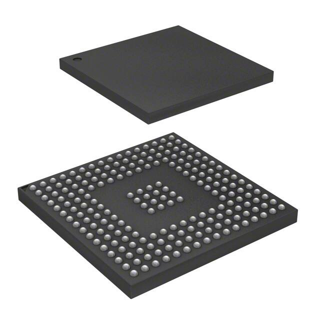
208 Ball Grid array (PBGA), 17mm x 17mm, 1mm pitch
Easily expandable in depth and width
Independent Read and Write Clocks (permit reading and writing
simultaneously)
High-performance submicron CMOS technology
Industrial temperature range (-40°°C to +85°°C) is available
Green parts available, see ordering information
FUNCTIONAL BLOCK DIAGRAM
D0 -Dn (x40, x20, x10)
WEN
WCS
SREN SEN SCLK
WCLK
WSDR
INPUT REGISTER
WRITE CONTROL
LOGIC
MRS
PRS
TCK
TRST
TMS
TDO
RAM ARRAY
16,384 x 40,
32,768 x 40
65,536 x 40
131,072 x 40
FWFT
FSEL0
FSEL1
READ POINTER
BUS
CONFIGURATION
OUTPUT REGISTER
RESET
LOGIC
Vref
RT
MARK
RSDR
READ
CONTROL
LOGIC
JTAG CONTROL
(BOUNDARY SCAN)
RCLK
REN
RCS
TDI
HSTL
FF/IR
PAF
EF/OR
PAE
FLAG
LOGIC
WRITE POINTER
BM
IW
OW
SI
SO
OFFSET REGISTER
HSTL I/0
CONTROL
EREN
OE
Q0 -Qn (x40, x20, x10)
5995 drw01
ERCLK
IDT and the IDT logo are registered trademarks of Integrated Device Technology, Inc. The TeraSync is a trademark of Integrated Device Technology, Inc.
COMMERCIAL AND INDUSTRIAL TEMPERATURE RANGES
FEBRUARY 2009
1
© 2009 Integrated Device Technology, Inc. All rights reserved. Product specifications subject to change without notice.
DSC-5995/11
�IDT72T4088/98/108/118 2.5V HIGH-SPEED TeraSync™ DDR/SDR FIFO 40-BIT
CONFIGURATION 16,384 x 40, 32,768 x 40, 65,536 x 40 and 131,072 x 40
COMMERCIAL AND INDUSTRIAL
TEMPERATURE RANGES
PIN CONFIGURATIONS
A1 BALL PAD CORNER
A
V CC
V CC
D38
D1
D4
D7
D9
GND
GND
Q1
Q3
Q5
Q7
Q9
VDDQ
VDDQ
D35
D36
D39
D2
D5
D8
HSTL
GND
GND
Q0
Q2
Q4
Q6
Q8
Q22
Q23
D34
D37
D0
D3
D6
V CC
V CC
GND
GND
VDDQ
VDDQ
VDDQ
VDDQ
Q20
Q21
Q24
D33
D32
D31
V CC
V CC
V CC
V CC
GND
GND
VDDQ
VDDQ
VDDQ
VDDQ
Q27
Q26
Q25
D30
TDI
TRST
GND
VDDQ
MARK
Q29
Q28
TCK
TMS
TDO
VDDQ
VDDQ
RCS
RT
REN
WCLK
FWFT
PAF
VDDQ
GND
GND
GND
GND
GND
VDDQ
OE
RCLK
WEN
WCS
FF/IR
VDDQ
GND
GND
GND
GND
GND
VDDQ
SCLK
SI
MRS
FSEL1
FSEL0
GND
GND
GND
GND
GND
GND
VDDQ
SEN
SREN
IW
BM
PRS
V CC
GND
GND
GND
GND
GND
VDDQ
SO
EREN
WSDR
RSDR
OW
V CC
GND
VDDQ
PAE
ERCLK
D27
D28
D29
V CC
VDDQ
EF/OR
Q30
Q31
D23
D20
D26
V CC
V CC
V CC
V CC
GND
GND
VDDQ
VDDQ
VDDQ
VDDQ
Q32
Q33
Q34
D24
D21
D18
GND
V CC
V CC
V CC
GND
GND
VDDQ
VDDQ
VDDQ
VDDQ
Q35
Q36
Q37
D25
D22
D19
D16
D14
D12
D10
GND
GND
Q19
Q17
Q15
Q13
Q11
Q38
Q39
V CC
V CC
VREF
D17
D15
D13
D11
GND
GND
Q18
Q16
Q14
Q12
Q10
VDDQ
VDDQ
1
2
3
4
5
6
7
8
9
10
11
12
13
14
15
B
C
D
E
F
G
H
J
K
L
M
N
P
R
T
16
5995 drw02
PBGA: 1mm pitch, 17mm x 17mm (BB208-1, order code: BB)
TOP VIEW
2
FEBRUARY 13, 2009
�IDT72T4088/98/108/118 2.5V HIGH-SPEED TeraSync™ DDR/SDR FIFO 40-BIT
CONFIGURATION 16,384 x 40, 32,768 x 40, 65,536 x 40 and 131,072 x 40
DESCRIPTION
COMMERCIAL AND INDUSTRIAL
TEMPERATURE RANGES
deasserted. Data will be read out of the FIFO on both rising and falling edge
of RCLK when and REN is asserted.
Both the input and output port can be selected for either 2.5V LVTTL or HSTL
operation. This can be achieved by tying the HSTL signal LOW for LVTTL or
HIGH for HSTL voltage operation. When the read port is setup for HSTL mode,
the Read Chip Select (RCS) input also has the benefit of disabling the read port
inputs, providing additional power savings.
There is the option of selecting different data rates on the input and output ports
of the device. There are a total of four combinations to choose from, Double Data
Rate to Double Data Rate (DDR to DDR), DDR to Single Data Rate (DDR to
SDR), SDR to DDR, and SDR to SDR. The rates can be set up using the WSDR
and RSDR pins. For example, to set up the input to output combination of DDR
to SDR, WSDR will be HIGH and RSDR will be LOW. Read and write operations
are initiated on the rising edge of RCLK and WCLK respectively, never on the
falling edge. If REN or WEN is asserted after a rising edge of clock, no read or
write operations will be possible on the falling edge of that same pulse.
An Output Enable (OE) input is provided for high-impedance control of the
outputs. A read Chip Select (RCS) input is also provided for synchronous
enable/disable of the read port control input, REN. The RCS input is synchronized to the read clock, and also provides high-impedance controls to the Qn
data outputs. When RCS is disabled, REN will be disabled internally and the
data outputs will be in High-Impedance. Unlike the Read Chip Select signal
however, OE is not synchronous to RCLK. Outputs are high-impedanced
shortly after a delay time when the OE transitions from LOW to HIGH.
The Echo Read Enable (EREN) and Echo Read Clock (ERCLK) outputs
are used to provide tighter synchronization between the data being transmitted
from the Qn outputs and the data being received by the input device. These
output signals from the read port are required for high-speed data communications. Data read from the read port is available on the output bus with respect
to EREN and ERCLK, which is useful when data is being read at high-speed
operations where synchronization is important.
The frequencies of both the RCLK and WCLK signals may vary from 0 to fMAX
with complete independence. There are no restrictions on the frequency of one
clock input with respect to another.
There are two possible timing modes of operation with these devices: IDT
Standard mode and First Word Fall Through (FWFT) mode.
In IDT Standard mode, the first word written to an empty FIFO will not appear
on the data output lines unless a specific read operation is performed. A read
operation, which consists of activating REN and enabling a rising RCLK edge,
will shift the word from internal memory to the data output lines. Be aware that
in Double Data Rate (DDR) mode only the IDT Standard mode is available.
In FWFT mode, the first word written to an empty FIFO is clocked directly to
the data output lines after three transitions of RCLK. A read operation does not
have to be performed to access the first word written to the FIFO. However,
subsequent words written to the FIFO do require a LOW on REN for access.
The state of the FWFT input during Master Reset determines the timing mode
in use.
For applications requiring more data storage capacity than a single FIFO can
provide, the FWFT timing mode permits depth expansion by chaining FIFOs
in series (i.e. the data outputs of one FIFO are connected to the corresponding
data inputs of the next). No external logic is required.
These FIFOs have four flag pins, EF/OR (Empty Flag or Output Ready), FF/
IR (Full Flag or Input Ready), PAE (Programmable Almost-Empty flag), and
PAF (Programmable Almost-Full flag). The EF and FF functions are selected
in IDT Standard mode. The IR and OR functions are selected in FWFT mode.
PAE and PAF are always available for use, irrespective of timing mode.
The IDT72T4088/72T4098/72T40108/72T40118 are exceptionally deep,
extremely high speed, CMOS First-In-First-Out (FIFO) memories with the ability
to read and write data on both rising and falling edges of clock. The device has
a flexible x40/x20/x10 Bus-Matching mode and the option to select single or
double data rates for input and output ports. These FIFOs offer several key user
benefits:
• Flexible x40/x20/x10 Bus-Matching on both read and write ports
• Ability to read and write on both rising and falling edges of a clock
• User selectable Single or Double Data Rate of input and output ports
• A user selectable MARK location for retransmit
• User selectable I/O structure for HSTL or LVTTL
• The first word data latency period, from the time the first word is written to
an empty FIFO to the time it can be read, is fixed and short.
• High density offerings up to 5Mbit
• 10Gbps throughput
Bus-Matching Double Data Rate FIFOs are particularly appropriate for
network, video, telecommunications, data communications and other applications that require fast data transfer on both rising and falling edges of the clock.
This is a great alternative to increasing data rate without extending the width of
the bus or the speed of the device. They are also effective in applications that
need to buffer large amounts of data and match buses of unequal sizes.
Each FIFO has a data input port (Dn) and a data output port (Qn), both of
which can assume either a 40-bit, 20-bit, or a 10-bit width as determined by the
state of external control pins Input Width (IW), Output Width (OW), and BusMatching (BM) pin during the Master Reset cycle.
The input port is controlled by a Write Clock (WCLK) input and a Write Enable
(WEN) input. Data present on the Dn data inputs can be written into the FIFO
on every rising and falling edge of WCLK when WEN is asserted and Write
Single Data Rate (WSDR) pin held HIGH. Data can be selected to write only
on the rising edges of WCLK if WSDR is asserted. To guarantee functionality
of the device, WEN must be a controlled signal and not tied to ground. This is
important because WEN must be HIGH during the time when the Master Reset
(MRS) pulse is LOW. In addition, the WSDR pin must be tied HIGH or LOW.
It is not a controlled signal and cannot be changed during FIFO operation.
Write operations can be selected for either Single or Double Data Rate mode.
For Single Data Rate operation, writing into the FIFO requires the Write Single
Data Rate (WSDR) pin to be asserted. Data will be written into the FIFO on the
rising edge of WCLK when the Write Enable (WEN) is asserted. For Double
Data Rate operations, writing into the FIFO requires WSDR to be deasserted.
Data will be written into the FIFO on both rising and falling edge of WCLK when
WEN is asserted.
The output port is controlled by a Read Clock (RCLK) input and a Read
Enable (REN) input. Data is read from the FIFO on every rising and falling edge
of RCLK when REN is asserted and Read Single Data Rate (RSDR) pin held
HIGH. Data can be selected to read only on the rising edges of RCLK if RSDR
is asserted. To guarantee functionality of the device, REN must be a controlled
signal and not tied to ground. This is important because REN must be HIGH
during the time when the Master Reset (MRS) pulse is LOW. In addition, the
RSDR pin must be tied HIGH or LOW. It is not a controlled signal and cannot
be changed during FIFO operation.
Read operations can be selected for either Single or Double Data Rate mode.
Similar to the write operations, reading from the FIFO in single data rate requires
the Read Single Data Rate (RSDR) pin to be asserted. Data will be read from
the FIFO on the rising edge of RCLK when the Read Enable (REN) is asserted.
For Double Data Rate operations, reading into the FIFO requires RSDR to be
3
FEBRUARY 13, 2009
�IDT72T4088/98/108/118 2.5V HIGH-SPEED TeraSync™ DDR/SDR FIFO 40-BIT
CONFIGURATION 16,384 x 40, 32,768 x 40, 65,536 x 40 and 131,072 x 40
DESCRIPTION (CONTINUED)
COMMERCIAL AND INDUSTRIAL
TEMPERATURE RANGES
not WCLK. Similarly the PAF is asserted and updated on the rising edge of
WCLK only and not RCLK.
This device includes a Retransmit from Mark feature that utilizes two control
inputs, MARK and RT (Retransmit). If the MARK input is enabled with respect
to the RCLK, the memory location being read at the point will be marked. Any
subsequent retransmit operation (when RT goes LOW), will reset the read
pointer to this “marked” location.
The device can be configured with different input and output bus widths as
previously stated. These rates are: x40 to x40, x40 to x20,x40 to x10, x20 to
x40, and x10 to x40.
If, at any time, the FIFO is not actively performing an operation, the chip will
automatically power down. Once in the power down state, the standby supply
current consumption is minimized. Initiating any operation (by activating control
inputs) will immediately take the device out of the power down state.
A JTAG test port is provided, here the FIFO has fully functional boundary
Scan feature, compliant with IEEE 1449.1 Standard Test Access Port and
Boundary Scan Architecture.
The Double Data Rate FIFO has the capability of operating in either LVTTL
or HSTL mode. HSTL mode can be selected by enabling the HSTL pin. Both
input and output ports will operate in either HSTL or LVTTL mode, but cannot
be selected independent of one another.
The IDT72T4088/72T4098/72T40108/72T40118 are fabricated using
IDT’s high-speed submicron CMOS technology.
PAE and PAF flags can be programmed independently to switch at any point
in memory. Programmable offsets mark the location within the internal memory
that activates the PAE and PAF flags and can only be programmed serially. To
program the offsets, set SEN active and data can be loaded via the Serial Input
(SI) pin at the rising edge of SCLK. To read out the offset registers serially, set
SREN active and data can be read out via the Serial Output (SO) pin at the rising
edge of SCLK. Four default offset settings are also provided, so that PAE can
be marked at a predefined number of locations from the empty boundary and
the PAF threshold can also be marked at similar predefined values from the full
boundary. The default offset values are set during Master Reset by the state
of the FSEL0 and FSEL1 pins.
During Master Reset (MRS), the following events occur: the read and write
pointers are set to the first location of the internal FIFO memory, the FWFT pin
selects IDT Standard mode or FWFT mode, the bus width configuration of the
read and write port is determined by the state of IW and OW, and the default offset
values for the programmable flags are set.
The Partial Reset (PRS) also sets the read and write pointers to the first
location of the memory. However, the timing mode and the values stored in the
programmable offset registers before Partial Reset remain unchanged. The
flags are updated according to the timing mode and offsets in effect. PRS is useful
for resetting a device in mid-operation, when reprogramming programmable
flags would be undesirable.
The timing of the PAE and PAF flags are synchronous to RCLK and WCLK,
respectively. The PAE flag is asserted upon the rising edge of RCLK only and
4
FEBRUARY 13, 2009
�IDT72T4088/98/108/118 2.5V HIGH-SPEED TeraSync™ DDR/SDR FIFO 40-BIT
CONFIGURATION 16,384 x 40, 32,768 x 40, 65,536 x 40 and 131,072 x 40
PARTIAL RESET (PRS)
COMMERCIAL AND INDUSTRIAL
TEMPERATURE RANGES
MASTER RESET (MRS)
WRITE CLOCK (WCLK)
READ CLOCK (RCLK)
WRITE ENABLE (WEN)
READ ENABLE (REN)
OUTPUT ENABLE (OE)
WRITE CHIP SELECT (WCS)
IDT
72T4088
72T4098
72T40108
72T40118
WRITE SINGLE DATA RATE (WSDR)
(x40, x20, x10) DATA IN (D0 - Dn)
READ CHIP SELECT (RCS)
READ SINGLE DATA RATE (RSDR)
(x40, x20, x10) DATA OUT (Q0 - Qn)
RCLK ECHO (ERCLK)
SERIAL CLOCK (SCLK)
REN ECHO (EREN)
SERIAL ENABLE(SEN)
MARK
SERIAL READ ENABLE(SREN)
FIRST WORD FALL THROUGH (FWFT)
SERIAL INPUT (SI)
RETRANSMIT (RT)
EMPTY FLAG/OUTPUT READY (EF/OR)
SERIAL OUTPUT (SO)
FULL FLAG/INPUT READY (FF/IR)
PROGRAMMABLE ALMOST-EMPTY (PAE)
PROGRAMMABLE ALMOST-FULL (PAF)
5995 drw03
OUTPUT WIDTH (OW)
INPUT WIDTH (IW)
Figure 1. Single Device Configuration Signal Flow Diagram
TABLE 1 — BUS-MATCHING CONFIGURATION MODES
BM
IW
OW
Write Port Width
Read Port Width
L
L
L
x40
x40
H
L
L
x40
x20
H
L
H
x40
x10
H
H
L
x20
x40
H
H
H
x10
x40
NOTE:
1. Pin status during Master Reset.
TABLE 2 — DATA RATE-MATCHING CONFIGURATION MODES
WSDR
RSDR
Write Port Width
Read Port Width
H
H
Double Data Rate
Double Data Rate
H
L
Double Data Rate
Single Data Rate
L
H
Single Data Rate
Double Data Rate
L
L
Single Data Rate
Single Data Rate
NOTE:
1. Pin status during Master Reset.
2. Data Rate Matching can be used in conjunction with Bus-Matching modes.
5
FEBRUARY 13, 2009
�IDT72T4088/98/108/118 2.5V HIGH-SPEED TeraSync™ DDR/SDR FIFO 40-BIT
CONFIGURATION 16,384 x 40, 32,768 x 40, 65,536 x 40 and 131,072 x 40
COMMERCIAL AND INDUSTRIAL
TEMPERATURE RANGES
PIN DESCRIPTION
Symbol &
Pin No.
BM(1)
(K2)
Name
Bus-Matching
I/O TYPE
LVTTL
INPUT
Description
During Master Reset, this pin along with IW and OW selects the bus sizes for both write and read
ports.
D0-D39
Data Inputs
(See Pin No.
table for details)
HSTL-LVTTL Data inputs for a 40-, 20-, or 10-bit bus. When in 20- or 10- bit mode, the unused input pins are in a don’t
INPUT
care state. The data bus is sampled on both rising and falling edges of WCLK when WEN is enabled and
DDR Mode is enabled or on the rising edges of WCLK only in SDR Mode.
EF/OR
(M14)
Empty Flag/
Output Ready
HSTL-LVTTL In the IDT Standard mode, the EF function is selected. EF indicates whether or not the FIFO memory
OUTPUT is empty. In FWFT mode, the OR function is selected. OR indicates whether or not there is valid data
available at the outputs.
ERCLK
(L16)
Echo Read
Clock
HSTL-LVTTL Read Clock Echo output, must be equal to or faster than the Qn data outputs.
OUTPUT
EREN
(K16)
Echo Read
Enable
HSTL-LVTTL Read Enable Echo output, used in conjunction with ERCLK.
OUTPUT
FF/IR
(H3)
Full Flag/
Input Ready
HSTL-LVTTL In the IDT Standard mode, the FF function is selected. FF indicates whether or not the FIFO memory is
OUTPUT empty. In FWFT mode, the IR function is selected. IR indicates whether or not there is space available
for writing to the FIFO memory.
FSEL0(1)
(J3)
Flag Select Bit 0
LVTTL
INPUT
During Master Reset, this input along with FSEL1 will select the default offset values for the programmable
flags PAE and PAF. There are four possible settings available.
FSEL1(1)
(J2)
Flag Select Bit 1
LVTTL
INPUT
During Master Reset, this input along with FSEL0 will select the default offset values for the programmable
flags PAE and PAF. There are four possible settings available.
FWFT
(G2)
First Word Fall
Through
LVTTL
INPUT
During Master reset, selects First Word Fall Through or IDT Standard mode. FWFT is not available in
DDR mode. In SDR mode, the first word will always fall through on the rising edge.
HSTL(1)
(B7)
HSTL Select
LVTTL
INPUT
This input pin is used to select HSTL or 2.5V LVTTL device operation. If HSTL inputs are required, this
input must be tied HIGH, otherwise it must be tied LOW and cannot toggle during operation.
IW(1)
(K1)
Input Width
LVTTL
INPUT
During Master Reset, this pin along with OW and BM, selects the bus width of the read and write port.
MARK
(E14)
Mark Read
Pointer for
Retransmit
HSTL-LVTTL When this pin is asserted the current location of the read pointer will be marked. Any subsequent Retransmit
INPUT
operation will reset the read pointer to this position. There is an unlimited number to times to set the mark
location, but only the most recent location marked will be acknowledged.
MRS
(J1)
Master Reset
HSTL-LVTTL MRS initializes the read and write pointers to zero and sets the output registers to all zeros. During Master
INPUT
Reset, the FIFO is configured for either FWFT or IDT Standard mode, Bus-Matching configurations, and
programmable flag default settings.
OE
(G15)
Output Enable
HSTL-LVTTL When HIGH, data outputs Q0-Q39 are in high impedance. When LOW, the data outputs Q0-Q39 are enabled.
INPUT
No other outputs are affected by OE.
OW(1)
(L3)
Output Width
PAE
(L15)
Programmable
Almost-Empty
Flag
PAF
(G3)
Programmable HSTL-LVTTL PAF goes HIGH if the number of free locations in the FIFO memory is more than offset m, which is stored
Almost-Full Flag
OUTPUT in the Full Offset register. PAF goes LOW if the number of free locations in the FIFO memory is less than
or equal to m.
PRS
(K3)
Partial Reset
HSTL-LVTTL PRS initializes the read and write pointers to zero and sets the output registers to all zeros. During Partial
INPUT
Reset, the existing mode (IDT standard or FWFT) and programmable flag settings are not affected.
Data Outputs
Q0-Q39
(See Pin No.
table for details)
HSTL-LVTTL Data outputs for a 40-, 20-, or 10-bit bus. When in 20- or 10- bit mode, the unused output pins should not
OUTPUT be connected. The output data is clocked on both rising and falling edges of RCLK when REN is enabled
and DDR Mode is enabled or on the rising edges of RCLK only in SDR Mode.
RCLK
(G16)
HSTL-LVTTL Input clock when used in conjunction with REN for reading data from the FIFO memory and output register.
INPUT
Read Clock
LVTTL
INPUT
During Master Reset, this pin along with IW and BM, selects the bus width of the read and write port.
HSTL-LVTTL PAE goes HIGH if the number of words in the FIFO memory is greater than or equal to offset n, which is
OUTPUT stored in the Empty Offset register. PAE goes LOW if the number of words in the FIFO memory is less than
offset n.
6
FEBRUARY 13, 2009
�IDT72T4088/98/108/118 2.5V HIGH-SPEED TeraSync™ DDR/SDR FIFO 40-BIT
CONFIGURATION 16,384 x 40, 32,768 x 40, 65,536 x 40 and 131,072 x 40
COMMERCIAL AND INDUSTRIAL
TEMPERATURE RANGES
PIN DESCRIPTION (CONTINUED)
Symbol &
Pin No.
RCS
(F14)
Name
I/O TYPE
Description
Read Chip Select HSTL-LVTTL RCS provides synchronous enable/disable control of the read port and High-Impedance control of the
INPUT
Qn data outputs, synchronous to RCLK. When using RCS the OE pin must be tied LOW. During Master
or Partial Reset the RCS input is don’t care, if OE is LOW the data outputs will be Low-Impedance
regardless of RCS.
REN
(F16)
Read Enable
HSTL-LVTTL When LOW and in DDR mode, REN along with a rising and falling edge of RCLK will send data in FIFO
INPUT
memory to the output register and read the current data in output register. In SDR mode data will only be
read on the rising edge of RCLK only.
RSDR(1)
(L2)
Read Single Data
Rate
RT
(F15)
Retransmit
SCLK
(H15)
Serial Clock
SEN
(J15)
Serial Input
Enable
HSTL-LVTTL SEN used in conjunction with SI and SCLK enables serial loading of the programmable flag offsets.
INPUT
SREN
(J16)
Serial Read
Enable
HSTL-LVTTL SREN used in conjunction with SO and SCLK enables serial reading of the programmable flag offsets.
INPUT
SI
(H16)
Serial Input
HSTL-LVTTL This input pin is used to load serial data into the programmable flag offsets. Used in conjunction with SEN
INPUT
and SCLK.
SO
(K15)
Serial Output
HSTL-LVTTL This output pin is used to read data from the programmable flag offsets. Used in conjunction with SREN
OUTPUT and SCLK.
TCK(2)
(F1)
JTAG Clock
HSTL-LVTTL Clock input for JTAG function. One of four terminals required by IEEE Standard 1149.1-1990. Test
INPUT
operations of the device are synchronous to TCK. Data from TMS and TDI are sampled on the rising edge
of TCK and outputs change on the falling edge of TCK. If the JTAG function is not used this signal needs
to be tied to GND.
TDI(2)
(E2)
JTAG Test Data
Input
HSTL-LVTTL One of four terminals required by IEEE Standard 1149.1-1990. During the JTAG boundary scan operation,
INPUT
test data serially loaded via the TDI on the rising edge of TCK to either the Instruction Register, ID Register
and Bypass Register. An internal pull-up resistor forces TDI HIGH if left unconnected.
TDO(2)
(F3)
JTAG Test Data
Output
HSTL-LVTTL One of four terminals required by IEEE Standard 1149.1-1990. During the JTAG boundary scan operation,
OUTPUT
test data serially loaded output via the TDO on the falling edge of TCK from either the Instruction Register,
ID Register and Bypass Register. This output is high impedance except when shifting, while in SHIFTDR and SHIFT-IR controller states.
TMS(2)
(F2)
JTAG Mode
Select
HSTL-LVTTL TMS is a serial input pin. One of four terminals required by IEEE Standard 1149.1-1990. TMS directs the
INPUT
the device through its TAP controller states. An internal pull-up resistor forces TMS HIGH if left unconnected.
TRST(2)
(E3)
JTAG Reset
HSTL-LVTTL TRST is an asynchronous reset pin for the JTAG controller. The JTAG TAP controller does not
INPUT
automatically reset upon power-up, thus it must be reset by either this signal or by setting TMS= HIGH for
five TCK cycles. If the TAP controller is not properly reset then the FIFO outputs will always be in highimpedance. If the JTAG function is used but the user does not want to use TRST, then TRST can be tied
with MRS to ensure proper FIFO operation. If the JTAG function is not used then this signal needs to be
tied to GND. An internal pull-up resistor forces TRST HIGH if left unconnected.
WCLK
(G1)
Write Clock
HSTL-LVTTL Input clock when used in conjunction with WEN for writing data into the FIFO memory.
INPUT
WCS
(H2)
Write Chip Select HSTL-LVTTL The WCS pin can be regarded as a second WEN input, enabling/disabling write operations.
INPUT
WEN
(H1)
Write Enable
LVTTL
INPUT
When LOW, this input pin sets the read port to Single Data Clock mode. When HIGH, the read port will operate
in Double Data Clock mode. This pin must be tied either HIGH or LOW and cannot toggle during operation.
HSTL-LVTTL RT asserted on the rising edge of RCLK initializes the read pointer to the first location in memory. EF flag
INPUT
is set to LOW (OR to HIGH in FWFT mode). The write pointer, offset registers, and flag settings are not
affected. If a mark has been set via the MARK input pin, then the read pointer will initialize to the mark location
when RT is asserted.
LVTTL
INPUT
A rising edge of SCLK will clock the serial data present on the SI input into the offset registers provided
that SEN is enabled. A rising edge of SCLK will also read data out of the offset registers provided that SREN
is enabled.
HSTL-LVTTL When LOW and in DDR mode, WEN along with a rising and falling edge of WCLK will write data into the
INPUT
FIFO memory. In SDR mode data will only be read on the rising edge of RCLK only.
7
FEBRUARY 13, 2009
�IDT72T4088/98/108/118 2.5V HIGH-SPEED TeraSync™ DDR/SDR FIFO 40-BIT
CONFIGURATION 16,384 x 40, 32,768 x 40, 65,536 x 40 and 131,072 x 40
COMMERCIAL AND INDUSTRIAL
TEMPERATURE RANGES
PIN DESCRIPTION (CONTINUED)
Symbol &
Pin No.
WSDR(1)
(L1)
Name
I/O TYPE
Description
Write Single Data
Rate
LVTTL
INPUT
When LOW, this input pin sets the write port to Single Data Clock mode. When HIGH, the write port will
operate in Double Data Clock mode. This pin must be tied either HIGH or LOW and cannot toggle
during operation.
V CC
(See below)
+2.5V Supply
INPUT
There are Vcc supply inputs and must be connected to the 2.5V supply rail.
VDDQ
(See below)
O/P Rail Voltage
INPUT
This pin should be tied to the desired voltage rail for providing power to the output drivers. Nominally 1.5V
or 1.8V for HSTL, 2.5V for LVTTL.
GND
(See below)
Core Ground Pin
INPUT
These are Ground pins are for the core device and must be connected to the GND rail.
Vref
(T3)
Reference
Voltage
INPUT
This is a Voltage Reference input and must be connected to a voltage level determined in the
Recommended DC Operating Conditions section. This provides the reference voltage when using HSTL
class inputs. If HSTL class inputs are not being used, this pin must be connected to GND.
NOTES:
1. Inputs should not change state after Master Reset.
2. These pins are for the JTAG port. Please refer to pages 25-28 and Figures 5-7.
PIN NUMBER TABLE
Symbol
Name
I/O TYPE
Pin Number
D0-39
Data Inputs
HSTL-LVTTL D0-C3, D1-A4, D2-B4, D3-C4, D4-A5, D5-B5, D6-C5, D7-A6, D8-B6, D9-A7, D10-R7, D11-T7,
INPUT
D12-R6, D13-T6, D14-R5, D15-T5, D16-R4, D17-T4, D18-P3, D19-R3, D20-N2, D21-P2, D22-R2,
D23-N1, D24-P1, D25-R1, D26-N3, D(27-29)-M(1-3), D30-E1, D(31-33)-D(3-1), D34-C1,
D(35,36)-B(1,2), D37-C2, D38-A3, D39-B3
Q0-39
Data Outputs
HSTL-LVTTL Q0-B10, Q1-A10, Q2-B11, Q3-A11, Q4-B12, Q5-A12, Q6-B13, Q7-A13, Q8-B14, Q9-A14, Q10-T14
OUTPUT Q11-R14, Q12-T13, Q13-R13, Q14-T12, Q15-R12, Q16-T11, Q17-R11, Q18-T10, Q19-R10,
Q(20,21)-C(14,15), Q(22,23)-B(15,16), Q24-C16, Q(25-27)-D(16-14), Q(28,29)-E(16,15),
Q(30,31)-M(15,16), Q(32-34)- N(14-16), Q(35-37)-P(14-16), Q(38,39)-R(15,16)
V CC
+2.5V Supply
INPUT
A(1,2), C(6,7), D(4-7), K4, L4, M4, N(4-7), P(5-7), T(1,2)
VDDQ
O/P Rail Voltage
INPUT
A(15,16), C(10-13), D(10-13), E13, F(4,13), G(4,14), H(4,14), J14, K14, L14, M13, N(10-13),
P(10-13), T(15,16)
GND
Ground Pin
INPUT
A(8,9), B(8,9), C(8,9), D(8,9), E4, G(7-10,13), H(7-10,13), J(4,7-10,13), K(7-10,13), L13, N(8,9),
P(4,8,9), R(8,9), T(8,9)
8
FEBRUARY 13, 2009
�IDT72T4088/98/108/118 2.5V HIGH-SPEED TeraSync™ DDR/SDR FIFO 40-BIT
CONFIGURATION 16,384 x 40, 32,768 x 40, 65,536 x 40 and 131,072 x 40
ABSOLUTE MAXIMUM RATINGS
COMMERCIAL AND INDUSTRIAL
TEMPERATURE RANGES
CAPACITANCE (TA = +25°C, f = 1.0MHz)
Symbol
VTERM
Rating
Terminal Voltage
with respect to GND
Commercial
–0.5 to +3.6(2)
Unit
V
TSTG
Storage Temperature
–55 to +125
°C
IOUT
DC Output Current
–50 to +50
mA
Symbol
CIN
(2,3)
COUT(1,2)
NOTES:
1. Stresses greater than those listed under ABSOLUTE MAXIMUM RATINGS may cause
permanent damage to the device. This is a stress rating only and functional operation
of the device at these or any other conditions above those indicated in the operational
sections of this specification is not implied. Exposure to absolute maximum rating
conditions for extended periods may affect reliability.
2. Compliant with JEDEC JESD8-5. VCC terminal only.
Parameter(1)
Conditions
Max.
(3)
Unit
Input
Capacitance
VIN = 0V
10
pF
Output
Capacitance
VOUT = 0V
10
pF
NOTES:
1. With output deselected, (OE ≥ VIH).
2. Characterized values, not currently tested.
3. CIN for Vref is 20pF.
RECOMMENDED DC OPERATING CONDITIONS
Symbol
VCC
VDDQ
GND
VIH
VIL
Parameter
Typ.
Max.
Unit
2.375
2.375
0
1.7
VREF+0.2
VREF+0.2
Min.
2.5
2.5
0
—
—
—
2.625
2.625
0
3.45
—
—
V
V
V
V
V
V
⎯ LVTTL
⎯ eHSTL
⎯ HSTL
-0.3
—
—
—
—
—
0.7
VREF-0.2
VREF-0.2
V
V
V
⎯ eHSTL
⎯ HSTL
0.8
0.68
0.9
0.75
1.0
0.9
V
V
0
—
70
°C
-40
—
85
°C
Supply Voltage
Output Rail Voltage for I/Os
Supply Voltage
Input High Voltage
⎯ LVTTL
⎯ eHSTL
⎯ HSTL
Input Low Voltage
VREF
Voltage Reference Input
(HSTL only)
TA
Operating Temperature Commercial
TA
Operating Temperature Industrial
NOTE:
1. VREF is only required for HSTL or eHSTL inputs. VREF should be tied LOW for LVTTL operation.
DC ELECTRICAL CHARACTERISTICS
(Commercial: VCC = 2.5V ± 0.125V, TA = 0°C to +70°C;Industrial: VCC = 2.5V ± 0.125V, TA = -40°C to +85°C)
Symbol
Parameter
ILI
Input Leakage Current
ILO
Output Leakage Current
VOH(5)
Output Logic “1” Voltage,
VOL
Output Logic “0” Voltage,
ICC1(1,2)
Active VCC Current (VCC = 2.5V)
ICC2(1)
Standby VCC Current (VCC = 2.5V)
Min.
Max.
Unit
–10
10
µA
–10
10
µA
VDDQ -0.4
VDDQ -0.4
VDDQ -0.4
—
—
—
—
—
—
0.4V
0.4V
0.4V
V
V
V
V
V
V
I/O = LVTTL
I/O = HSTL
I/O = eHSTL
—
—
—
20
60
60
mA
mA
mA
I/O = LVTTL
I/O = HSTL
I/O = eHSTL
—
—
—
10
50
50
mA
mA
mA
IOH = –8 mA @VDDQ = 2.5V ± 0.125V (LVTTL)
IOH = –8 mA @VDDQ = 1.8V ± 0.1V (eHSTL)
IOH = –8 mA @VDDQ = 1.5V ± 0.1V (HSTL)
IOL = 8 mA @VDDQ = 2.5V ± 0.125V (LVTTL)
IOL = 8 mA @VDDQ = 1.8V ± 0.1V (eHSTL)
IOL = 8 mA @VDDQ = 1.5V ± 0.1V (HSTL)
NOTES:
1. Both WCLK and RCLK toggling at 20MHz. Data inputs toggling at 10MHz. WCS = HIGH, REN or RCS = HIGH.
2. Typical ICC1 calculation: for LVTTL I/O ICC1 (mA) = 0.6mA x fs, fs = WCLK frequency = RCLK frequency (in MHz)
for HSTL or eHSTL I/O ICC1 (mA) = 38mA + (0.7mA x fs), fs = WCLK frequency = RCLK frequency (in MHz)
3. Typical IDDQ calculation: With Data Outputs in High-Impedance: IDDQ (mA) = 0.15mA x fs
With Data Outputs in Low-Impedance: IDDQ (mA) = (CL x VDDQ x fs x 2N)/2000
fs = WCLK frequency = RCLK frequency (in MHz), VDDQ = 2.5V for LVTTL; 1.5V for HSTL; 1.8V for eHSTL, N = Number of outputs switching.
tA = 25°C, CL = capacitive load (pf)
4. Total Power consumed: PT = [(VCC x ICC) + (VDDQ x IDDQ)].
5. Outputs are not 3.3V tolerant.
9
FEBRUARY 13, 2009
�IDT72T4088/98/108/118 2.5V HIGH-SPEED TeraSync™ DDR/SDR FIFO 40-BIT
CONFIGURATION 16,384 x 40, 32,768 x 40, 65,536 x 40 and 131,072 x 40
COMMERCIAL AND INDUSTRIAL
TEMPERATURE RANGES
AC ELECTRICAL CHARACTERISTICS(1)
(Commercial: VCC = 2.5V ± 5%, TA = 0°C to +70°C;Industrial: VCC = 2.5V ± 5%, TA = -40°C to +85°C)
Symbol
fS1
fS2
tA
tASO
tCLK1
tCLK2
tCLKH1
tCLKH2
tCLKL1
tCLKL2
tDS
tDH
tENS
tENH
tWCSS
tWCSH
fC
tSCLK
tSCKH
tSCKL
tSDS
tSDH
tSENS
tSENH
tRS
tRSS
tHRSS
tRSR
tRSF
tOLZ
tOE
tOHZ
tWFF
tREF
tPAFS
tPAES
tERCLK
tCLKEN
tRCSLZ
tRCSHZ
tSKEW1
tSKEW2
tSKEW3
Parameter
Clock Cycle Frequency SDR
Clock Cycle Frequency DDR
Data Access Time
Data Access Serial Output Time
Clock Cycle Time SDR
Clock Cycle Time DDR
Clock High Time SDR
Clock High Time DDR
Clock Low Time SDR
Clock Low Time DDR
Data Setup Time
Data Hold Time
Enable Setup Time
Enable Hold Time
WCS setup time
WCS hold time
Clock Cycle Frequency (SCLK)
Serial Clock Cycle
Serial Clock High
Serial Clock Low
Serial Data In Setup
Serial Data In Hold
Serial Enable Setup
Serial Enable Hold
Reset Pulse Width(3)
Reset Setup Time
HSTL Reset Setup Time
Reset Recovery Time
Reset to Flag and Output Time
Output Enable to Output in Low Z(4)
Output Enable to Output Valid
Output Enable to Output in High Z(4)
Write Clock to FF or IR
Read Clock to EF or OR
Write Clock to Programmable Almost-Full Flag
Read Clock to Programmable Almost-Empty Flag
RCLK to Echo RCLK output
RCLK to Echo REN output
RCLK to Active from High-Z
RCLK to High-Z(4)
Skew time between RCLK and WCLK for EF/OR and FF/IR
Skew time between RCLK & WCLK for EF/OR & FF/IR in DDR mode
Skew time between RCLK and WCLK for PAE and PAF
Commercial
IDT72T4088L4
IDT72T4098L4
IDT72T40108L4
IDT72T40118L4
Min.
Max.
—
250
—
110
0.6
3.2
0.6
3.2
4
—
9.1
—
1.8
—
4.0
—
1.8
—
4.0
—
1.2
—
0.5
—
1.2
—
0.5
—
1.2
—
0.5
—
—
10
100
—
45
—
45
—
15
—
5
—
5
—
5
—
30
—
15
—
4
—
10
—
—
10
0
—
—
3.2
—
3.2
—
3.2
—
3.2
—
3.2
—
3.2
—
3.6
—
3.2
—
3.2
—
3.2
3.5
—
3.5
—
4
—
Commercial
IDT72T4088L5
IDT72T4098L5
IDT72T40108L5
IDT72T40118L5
Min.
Max.
—
200
—
100
0.6
3.6
0.6
3.6
5
—
10
—
2.3
—
4.5
—
2.3
—
4.5
—
1.5
—
0.5
—
1.5
—
0.5
—
1.5
—
0.5
—
—
10
100
—
45
—
45
—
15
—
5
—
5
—
5
—
30
—
15
—
4
—
10
—
—
12
0
—
—
3.6
—
3.6
—
3.6
—
3.6
—
3.6
—
3.6
—
4
—
3.6
—
3.6
—
3.6
4
—
4
—
5
—
Com’l & Ind’l(2)
Commercial
IDT72T4088L6-7 IDT72T4088L10
IDT72T4098L6-7 IDT72T4098L10
IDT72T40108L6-7 IDT72T40108L10
IDT72T40118L6-7 IDT72T40118L10
Min.
Max.
Min.
Max.
Unit
—
150
—
100
MHz
—
75
—
50
MHz
0.6
3.8
0.6
4.5
ns
0.6
3.8
0.6
4.5
ns
6.7
—
10
—
ns
13
—
20
—
ns
2.8
—
4.5
—
ns
6.0
—
9.5
—
ns
2.8
—
4.5
—
ns
6.0
—
9.5
—
ns
2.0
—
3.0
—
ns
0.5
—
0.5
—
ns
2.0
—
3.0
—
ns
0.5
—
0.5
—
ns
2.0
—
3.0
—
ns
0.5
—
0.5
—
ns
—
10
—
10
MHz
100
—
100
—
ns
45
—
45
—
ns
45
—
45
—
ns
15
—
15
—
ns
5
—
5
—
ns
5
—
5
—
ns
5
—
5
—
ns
30
—
30
—
ns
15
—
15
—
ns
4
—
4
—
µs
10
—
10
—
ns
—
15
—
15
ns
0
—
0
—
ns
—
3.8
—
4.5
ns
—
3.8
—
4.5
ns
—
3.8
—
4.5
ns
—
3.8
—
4.5
ns
—
3.8
—
4.5
ns
—
3.8
—
4.5
ns
—
4.3
—
5
ns
—
3.8
—
4.5
ns
—
3.8
—
4.5
ns
—
3.8
—
4.5
ns
5
—
7
—
ns
5
—
7
—
ns
6
—
8
—
ns
NOTES:
1. All AC timings apply to both IDT Standard mode and First Word Fall Through mode.
2. Industrial temperature range product for the 6-7ns speed grade is available as a standard device. All other speed grades are available by special order.
3. Pulse widths less than minimum values are not allowed.
4. Values guaranteed by design, not currently tested.
10
FEBRUARY 13, 2009
�IDT72T4088/98/108/118 2.5V HIGH-SPEED TeraSync™ DDR/SDR FIFO 40-BIT
CONFIGURATION 16,384 x 40, 32,768 x 40, 65,536 x 40 and 131,072 x 40
COMMERCIAL AND INDUSTRIAL
TEMPERATURE RANGES
AC TEST LOADS
HSTL
1.5V AC TEST CONDITIONS
Input Pulse Levels
Input Rise/Fall Times
Input Timing Reference Levels
Output Reference Levels
VDDQ/2
0.25 to 1.25V
0.4ns
0.75V
0.75V
50Ω
I/O
Z0 = 50Ω
10pF
NOTE:
1. VDDQ = 1.5V±.
5995 drw04
Figure 2a. AC Test Load
EXTENDED HSTL
1.8V AC TEST CONDITIONS
5
0.4 to 1.4V
0.4ns
0.9V
0.9V
tCD
(Typical, ns)
Input Pulse Levels
Input Rise/Fall Times
Input Timing Reference Levels
Output Reference Levels
6
4
3
2
1
NOTE:
1. VDDQ = 1.8V±.
20 30 50
200
5995 drw04a
Figure 2b. Lumped Capacitive Load, Typical Derating
2.5V LVTTL
2.5V AC TEST CONDITIONS
Input Pulse Levels
Input Rise/Fall Times
Input Timing Reference Levels
Output Reference Levels
80 100
Capacitance (pF)
GND to 2.5V
1ns
1.25V
1.25V
NOTE:
1. For LVTTL VCC = VDDQ.
11
FEBRUARY 13, 2009
�IDT72T4088/98/108/118 2.5V HIGH-SPEED TeraSync™ DDR/SDR FIFO 40-BIT
CONFIGURATION 16,384 x 40, 32,768 x 40, 65,536 x 40 and 131,072 x 40
COMMERCIAL AND INDUSTRIAL
TEMPERATURE RANGES
OUTPUT ENABLE & DISABLE TIMING
Output
Enable
Output
Disable
VIH
OE
VIL
tOE & tOLZ
Output VCC
Normally
2
LOW
tOHZ
VCC
2
100mV
100mV
VOL
VOH
100mV
Output
Normally VCC
HIGH 2
100mV
NOTES:
1. REN is HIGH.
2. RCS is LOW.
VCC
2
5995 drw04b
READ CHIP SELECT ENABLE & DISABLE TIMING
VIH
tENH
RCS
VIL
tENS
RCLK
tRCSHZ
tRCSLZ
Output VCC
Normally
2
LOW
Output
Normally VCC
HIGH 2
VCC
2
100mV
100mV
VOL
VOH
100mV
100mV
VCC
2
5995 drw04c
NOTES:
1. REN is HIGH.
2. OE is LOW.
12
FEBRUARY 13, 2009
�IDT72T4088/98/108/118 2.5V HIGH-SPEED TeraSync™ DDR/SDR FIFO 40-BIT
CONFIGURATION 16,384 x 40, 32,768 x 40, 65,536 x 40 and 131,072 x 40
FUNCTIONAL DESCRIPTION
COMMERCIAL AND INDUSTRIAL
TEMPERATURE RANGES
If the FIFO is full, the first read operation will cause FF to go HIGH. Subsequent
read operations will cause PAF to go HIGH at the conditions described in Table
4 If further read operations occur, without write operations, PAE will go LOW
when there are n words in the FIFO, where n is the empty offset value.
Continuing read operations will cause the FIFO to become empty. Then the last
word has been read from the FIFO, the EF will go LOW inhibiting further read
operations. REN is ignored when the FIFO is empty.
When configured in IDT Standard mode, the EF and FF outputs are double
register-buffered outputs. IDT Standard mode is available when the device is
configured in both Single Data Rate and Double Data Rate mode.
Relevant timing diagrams for IDT Standard mode can be found in Figure 10,
11, 12, 13, 14, 15, 16, 17, 18 and 23.
TIMING MODES: IDT STANDARD vs FIRST WORD FALL THROUGH
(FWFT) MODE
The IDT72T4088/72T4098/72T40108/72T40118 support two different
timing modes of operation: IDT Standard mode or First Word Fall Through
(FWFT) mode. The selection of which mode will operate is determined during
Master Reset, by the state of the FWFT input.
During Master Reset, if the FWFT pin is LOW, then IDT Standard mode will
be selected. This mode uses the Empty Flag (EF) to indicate whether or not there
are any words present in the FIFO. It also uses the Full Flag function (FF) to
indicate whether or not the FIFO has any free space for writing. In IDT Standard
mode, every word read from the FIFO, including the first, must be requested
using the Read Enable (REN) and RCLK.
If the FWFT pin is HIGH during Master Reset, then FWFT mode will be
selected. This mode uses Output Ready (OR) to indicate whether or not there
is valid data at the data outputs (Qn). It also uses Input Ready (IR) to indicate
whether or not the FIFO has any free space for writing. In the FWFT mode, the
first word written to an empty FIFO goes directly to Qn after three RCLK rising
edges, applying REN = LOW is not necessary. However, subsequent words
must be accessed using the Read Enable (REN) and RCLK.
Various signals, in both inputs and outputs operate differently depending on
which timing mode is in effect.
FIRST WORD FALL THROUGH MODE (FWFT)
In this mode, the status flags OR, IR, PAE, and PAF operate in the manner
outlined in Table 5. To write data into to the FIFO, WEN must be LOW. Data
presented to the DATA IN lines will be clocked into the FIFO on subsequent
transitions of WCLK. After the first write is performed, the Output Ready (OR)
flag will go LOW. Subsequent writes will continue to fill up the FIFO. PAE will go
HIGH after n + 2 words have been loaded into the FIFO, where n is the empty
offset value. The default setting for these values are listed in Table 3. This
parameter is also user programmable. See section on Programmable Flag
Offset Loading.
Continuing to write data into the FIFO without performing read operations will
cause the Programmable Almost-Full flag (PAF) to go LOW. Again, if no reads
are performed, the PAF will go LOW after (16,385-m) writes for the IDT72T4088,
(32,769-m) writes for the IDT72T4098, (65,537-m) writes for the IDT72T40108
and (131,073-m) writes for the IDT72T40118. The offset “m” is the full offset
value. The default setting for these values are listed in Table 3. This parameter is
also user programmable. See the section on Programmable Flag Offset Loading.
When the FIFO is full, the Input Ready (IR) will go LOW, inhibiting further write
operations. If no reads are performed after a reset, IR will go LOW after D writes
to the FIFO. D = 16,385 writes for the IDT72T4088, 32,769 writes for the
IDT72T4098, 65,537 writes for the IDT72T40108 and 131,073 writes for the
IDT72T40118, respectively. Note that the additional word in FWFT mode is due
to the capacity of the memory plus output register.
If the FIFO is full, the first read operation will cause IR to go HIGH. Subsequent
read operations will cause PAF to go HIGH at the conditions described in Table
5. If further read operations occur, without write operations, PAE will go LOW
when there are n words in the FIFO, where n is the empty offset value.
Continuing read operations will cause the FIFO to become empty. Then the last
word has been read from the FIFO, the OR will go HIGH inhibiting further read
operations. REN is ignored when the FIFO is empty.
When configured in FWFT mode, the OR flag output is triple register-buffered
and the IR flag output is double register-buffered. FWFT mode is only available
when the device is configured in Single Data Rate mode.
Relevant timing diagrams for IDT Standard mode can be found in Figure 19,
20, 21, 22 and 24.
IDT STANDARD MODE
In this mode, the status flags FF, PAF, PAE, and EF operate in the manner
outlined in Table 4. To write data into the FIFO, Write Enable (WEN) must be
LOW. Data presented to the DATA IN lines will be clocked into the FIFO on
subsequent transitions of the Write Clock (WCLK). After the first write is
performed, the Empty Flag (EF) will go HIGH. Subsequent writes will continue
to fill up the FIFO. The Programmable Almost-Empty flag (PAE) will go HIGH
after n + 1 words have been loaded into the FIFO, where n is the empty offset
value. The default setting for these values are listed in Table 3. This parameter
is also user programmable. See section on Programmable Flag Offset Loading.
Continuing to write data into the FIFO without performing read operations will
cause the Programmable Almost-Full flag (PAF) to go LOW. Again, if no reads
are performed, the PAF will go LOW after (16,384-m) writes for the IDT72T4088,
(32,768-m) writes for the IDT72T4098, (65,536-m) writes for the IDT72T40108
and (131,072-m) writes for the IDT72T40118. The offset “m” is the full offset
value. The default setting for these values are listed in Table 3. This parameter
is also user programmable. See the section on Programmable Flag Offset
Loading.
When the FIFO is full, the Full Flag (FF) will go LOW, inhibiting further write
operations. If no reads are performed after a reset, FF will go LOW after D writes
to the FIFO. D = 16,384 writes for the IDT72T4088, 32,768 writes for the
IDT72T4098, 65,536 writes for the IDT72T40108 and 131,072 writes for the
IDT72T40118, respectively.
13
FEBRUARY 13, 2009
�IDT72T4088/98/108/118 2.5V HIGH-SPEED TeraSync™ DDR/SDR FIFO 40-BIT
CONFIGURATION 16,384 x 40, 32,768 x 40, 65,536 x 40 and 131,072 x 40
TABLE 3 — DEFAULT PROGRAMMABLE
FLAG OFFSETS
IDT72T4088, 72T4098, 72T40108, 72T40118
FSEL1
H
L
H
L
FSEL0
H
H
L
L
Offsets n,m
255
127
63
7
NOTES:
1. n = empty offset for PAE.
2. m = full offset for PAF.
PROGRAMMING FLAG OFFSETS
Full and Empty Flag offset values are user programmable. The IDT72T4088/
72T4098/72T40108/72T40118 have internal registers for these offsets. There
are four selectable default offset values during Master Reset. These offset values
are shown in Table 3. The offset values can also be programmed serially into
the FIFO. To load offset values, set SEN LOW and the rising edge of SCLK will
COMMERCIAL AND INDUSTRIAL
TEMPERATURE RANGES
load data from the SI input into the offset registers. SCLK runs at a nominal speed
of 10MHz at the maximum. The programming sequence starts with one bit for
each SCLK rising edge, starting with the Empty Offset LSB and ending with the
Full Offset MSB. The total number of bits per device is listed in Figure 3,
Programmable Flag Offset Programming Sequence. See Figure 25, Loading
of Programmable Flag Registers, for the timing diagram for this mode. The PAE
and PAF can show a valid status only after the complete set of bits (for all offset
registers) has been entered. The registers can be reprogrammed as long as
the complete set of new offset bits is entered.
In addition to loading offset values into the FIFO, it is also possible to read
the current offset values. Similar to loading offset values, set SREN LOW and
the rising edge of SCLK will send data from the offset registers out to the SO output
port. When initializing a read to the offset registers, data will be read starting from
the first location in the register, regardless of where it was last read.
Figure 3, Programmable Flag Offset Programming Sequence, summarizes
the control pins and sequence for programming offset registers and reading and
writing into the FIFO.
The offset registers may be programmed (and reprogrammed) any time
after Master Reset. Valid programming ranges are from 0 to D-1.
TABLE 4 ⎯ STATUS FLAGS FOR IDT STANDARD MODE
IDT72T4098
IDT72T4088
Number of
Words in
FIFO
IDT72T40108
IDT72T40118
FF
PAF PAE EF
0
0
0
0
H
H
L
1 to n (1)
1 to n (1)
1 to n (1)
1 to n (1)
H
H
L
H
H
H
H
H
(131,072-m) to 131,071
H
L
H
H
65,536
131,072
L
L
H
H
IDT72T40118
(8,193) to (16,384-(m+1))
(16,384-m) to 16,383
(16,385) to (32,768-(m+1))
(32,768-m) to 32,767
16,384
(32,769) to (65,536-(m+1)) (65,537) to (131,072-(m+1))
(65,536-m) to 65,535
32,768
L
NOTE:
1. See table 3 for values for n, m.
TABLE 5 ⎯ STATUS FLAGS FOR FWFT MODE
Number of
Words in
FIFO
IDT72T4088
IDT72T4098
IDT72T40108
0
0
0
1 to n+1
(1)
(8,194) to (16,385-(m+1))
(16,385-m) to 16,384
1 to n+1
(1)
(16,386) to (32,769-(m+1))
(32,769-m) to 32,768
16,385
1 to n+1
0
(1)
(65,537-m) to 65,536
65,537
PAF PAE OR
L
H
L
L
H
L
L
L
H
H
L
(131,073-m) to 131,072
L
L
H
L
131,073
H
L
H
L
1 to n+1
(1)
(32,770) to (65,537-(m+1)) (65,538) to (131,073-(m+1))
32,769
IR
H
5995 drw05
NOTE:
1. See table 3 for values for n, m.
2. FWFT mode available only in Single Data Rate mode.
14
FEBRUARY 13, 2009
�IDT72T4088/98/108/118 2.5V HIGH-SPEED TeraSync™ DDR/SDR FIFO 40-BIT
CONFIGURATION 16,384 x 40, 32,768 x 40, 65,536 x 40 and 131,072 x 40
WSDR
RSDR
WEN
REN
SEN
SREN
WCLK
RCLK
X
X
1
1
0
1
X
X
X
X
1
1
1
COMMERCIAL AND INDUSTRIAL
TEMPERATURE RANGES
IDT72T4088
IDT72T4098
IDT72T40108
IDT72T40118
SCLK
Serial write to registers:
0
X
X
In SDR Mode
28 bits for the IDT72T4088
30 bits for the IDT72T4098
32 bits for the IDT72T40108
34 bits for the IDT72T40118
1 bit for each rising SCLK edge
Starting with Empty Offset
(LSB) Ending with Full Offset
(MSB)
Serial write to registers:
In DDR Mode
26 bits for the IDT72T4088
28 bits for the IDT72T4098
30 bits for the IDT72T40108
32 bits for the IDT 72T40118
1 bit for each rising SCLK edge
Starting with Empty Offset
(LSB) Ending with Full Offset
(MSB)
Serial read from registers:
Serial read from registers:
In SDR Mode
28 bits for the IDT72T4088
30 bits for the IDT72T4098
32 bits for the IDT72T40108
34 bits for the IDT72T40118
1 bit for each rising SCLK edge
Starting with Empty Offset
(LSB) Ending with Full Offset
(MSB)
In DDR Mode
26 bits for the IDT72T4088
28 bits for the IDT72T4098
30 bits for the IDT72T40108
32 bits for the IDT72T40118
1 bit for each rising SCLK edge
Starting with Empty Offset
(LSB) Ending with Full Offset
(MSB)
1
1
0
1
X
X
X
X
Write Memory (DDR)
0
1
0
1
X
X
X
X
Write Memory (SDR)
1
1
1
0
X
X
X
X
Read Memory (DDR)
1
0
1
0
X
X
X
X
Read Memory (SDR)
X
X
1
1
X
X
X
X
No Operation
X
5995 drw06
NOTES:
1. The programming sequence applies to both IDT Standard and FWFT modes.
2. When the input or output ports are in DDR mode, the depth is reduced by half but the overall density remains the same. For example, the IDT72T4088 in SDR mode is
16,384 x 40 = 655,360, in DDR mode the configuration becomes 8,192 x 80 = 655,360. In both cases, the total density are the same.
Figure 3. Programmable Flag Offset Programming Sequence
15
FEBRUARY 13, 2009
�IDT72T4088/98/108/118 2.5V HIGH-SPEED TeraSync™ DDR/SDR FIFO 40-BIT
CONFIGURATION 16,384 x 40, 32,768 x 40, 65,536 x 40 and 131,072 x 40
RETRANSMIT FROM MARK OPERATION
The Retransmit from Mark feature allows FIFO data to be read repeatedly
starting at a user-selected position. The FIFO is first put into retransmit mode
that will “mark” a beginning word and also set a pointer that will prevent
ongoing FIFO write operations from over-writing retransmit data. The retransmit data can be read repeatedly any number of times from the “marked”
position. The FIFO can be taken out of retransmit mode at any time to allow
normal device operation. The “mark” position can be selected any number of
times, each selection over-writing the previous mark location.
In Double Data Rate, data is always marked in pairs. That is, the unit of data
read on the rising and falling edge of WCLK. If the data marked was read on
the falling edge of RCLK, then the marked data will be the unit of data read from
the rising and falling edge of that particular RCLK edge. Refer to Figure 23,
Retransmit from Mark in Double Data Rate Mode, for the timing diagram in
this mode. Retransmit operation is available in both IDT standard and FWFT
modes.
During IDT standard mode the FIFO is put into retransmit mode by a Lowto-High transition on RCLK when the MARK input is HIGH and EF is HIGH.
The rising RCLK edge marks the data present in the FIFO output register as
the first retransmit data. Again, the data is marked in pairs. Thus if the data
marked was read on the falling edge of RCLK, the first part of retransmit will
read out the data read on the rising edge of RCLK, followed by the data on the
falling edge (the marked data). The FIFO remains in retransmit mode until a
rising edge on RCLK occurs while MARK is LOW.
Once a marked location has been set, a retransmit can be initiated by a
rising edge on RCLK while the Retransmit input (RT) is LOW. REN must be
HIGH (reads disabled) before bringing RT LOW. The device indicates the start
of retransmit setup by setting EF LOW, also preventing reads. When EF goes
HIGH, retransmit setup is complete and read operations may begin starting
with the first unit of data at the MARK location. Since IDT standard mode is
selected, every word read including the first “marked” word following a retransmit setup requires a LOW on REN.
Note, write operations may continue as normal during all retransmit functions,
however write operations to the “marked” location will be prevented. See Figure
COMMERCIAL AND INDUSTRIAL
TEMPERATURE RANGES
23, Retransmit from Mark in Double Data Rate Mode, for the relevant timing
diagram.
During FWFT mode the FIFO is put into retransmit mode by a rising RCLK
edge when the MARK input is HIGH and OR is LOW. The rising RCLK edge
marks the data present in the FIFO output register as the first retransmit data.
The data is marked in pairs. The FIFO remains in retransmit mode until a
rising RCLK edge occurs while MARK is LOW.
Once a marked location has been set, a retransmit can be initiated by a
rising RCLK edge while the Retransmit input (RT) is LOW. REN must be
HIGH (reads disabled) before bringing RT LOW. The device indicates the
start of retransmit setup by setting OR HIGH, preventing read operations.
When OR goes LOW, retransmit setup is complete and on the next rising
RCLK edge (RT goes HIGH), the contents of the first retransmit location are
loaded onto the output register. Since FWFT mode is selected, the first word
appears on the outputs regardless of REN, a LOW on REN is not required for
the first word. Reading all subsequent words requires a LOW on REN to
enable the rising RCLK edge. See Figure 24, Retransmit from Mark (FWFT
mode) for the relevant timing diagram.
Before a retransmit can be performed, there must be at least 1280 bits
(or 160 bytes) of data between the write pointer and mark location.
That is, 40 bits x32 for the x40 mode, 20 bits x64 for the x20 mode, and 10 bits
x128 for the x10 mode. Also, once the Mark is set, the write pointer will not
increment past the marked location, preventing overwrites of retransmit data.
HSTL/LVTTL I/O
This device supports both LVTTL and HSTL logic levels on the input and
output signals. If LVTTL is desired, a LOW on the HSTL pin will set the inputs
and outputs to LVTTL mode. If HSTL is desired, a HIGH on the HSTL pin will
set the inputs and outputs to HSTL mode. VREF is the input voltage reference
used in HSTL mode. Typically a logic HIGH in HSTL would be Vref + 0.2V and
a logic LOW would be VREF – 0.2V. Table 6 illustrates which pins are and are
not associated with this feature. Note that all “Static Pins” must be tied to Vcc or
GND. These pins are LVTTL only and are purely device configuration pins.
TABLE 6 — I/O CONFIGURATION
HSTL SELECT
STATIC PINS
HIGH = HSTL
LOW = LVTTL
LVTTL ONLY
Write Port
Dn (I/P)
WCLK (I/P)
WEN (I/P)
WCS (I/P)
Read Port
Qn (O/P)
RCLK (I/P)
REN (I/P)
RCS (I/P)
MARK (I/P)
OE (I/P)
RT (I/P)
Signal Pins
EF/OR (O/P)
PAF (O/P)
PAE (O/P)
FF/IR (O/P)
ERCLK (O/P)
EREN (O/P)
SCLK (I/P)
SI (I/P)
SO (O/P)
MRS (I/P)
PRS (I/P)
TCK (I/P)
TMS (I/P)
16
TRST (I/P)
TDI (I/P)
TDO (O/P)
SEN (I/P)
SREN (I/P)
Static Pins
IW (I/P)
OW (I/P)
BM ((I/P)
HSTL (I/P)
FSEL1 (I/P)
FSEL0 (I/P)
FWFT (I/P)
WSDR (I/P)
RSDR (I/P)
FEBRUARY 13, 2009
�IDT72T4088/98/108/118 2.5V HIGH-SPEED TeraSync™ DDR/SDR FIFO 40-BIT
CONFIGURATION 16,384 x 40, 32,768 x 40, 65,536 x 40 and 131,072 x 40
SIGNAL DESCRIPTION
COMMERCIAL AND INDUSTRIAL
TEMPERATURE RANGES
If FWFT mode has been selected, the OR flag will go HIGH on the rising
edge of RCLK that retransmit was initiated. OR will return LOW on the next
rising edge of RCLK, which signifies that retransmit setup is complete. Under
FWFT mode, the contents in the marked memory location will be loaded onto
the output register on the next rising edge of RCLK. To access all subsequent
data, a read operation will be required.
Subsequent retransmit operations may be performed, each time the read
pointer returning to the “marked” location. See Figure 24, Retransmit from
Mark (FWFT Mode) for the relevant timing diagram.
INPUTS:
DATA IN (D0 – Dn)
(D0 – D39) are data inputs for the 40-bit wide data, (D0 – D19) are data
inputs for the 20-bit wide data, or (D0 – D9) are data inputs for 10-bit wide data.
CONTROLS:
MASTER RESET (MRS)
A Master Reset is accomplished whenever the MRS input is taken to a LOW
state. This operation sets the internal read and write pointers to the first location
of the RAM array. PAE will go LOW and PAF will go HIGH.
If FWFT is LOW during Master Reset then IDT Standard mode along with
EF and FF are selected. EF will go LOW and FF will go HIGH, If FWFT is
HIGH, then the First Word Fall Through (FWFT) mode, along with IR and OR
are selected. OR will go HIGH and IR will go LOW.
All control settings such as OW, IW, BM, WSDR, RSDR, FSEL0 and FSEL1
are defined during the Master Reset cycle.
During a Master Reset the output register is initialized to all zeros. A Master
Reset is required after power up before a write operation can take place. MRS
is asynchronous.
See Figure 8, Master Reset Timing, for the relevant timing diagram.
MARK
The MARK input is used to select Retransmit mode of operation. On a rising
edge of RCLK while MARK is HIGH will mark the memory location of the data
currently present on the output register, in addition placing the device in
retransmit mode. Note, there must be a minimum of 1280 bits (or 160 bytes) of
data between the write pointer and mark location. That is, 40 bits x32 for the
x40 mode, 20 bits x64 for the x20 mode, and 10 bits x128 for the x10 mode.
Also, once the MARK is set, the write pointer will not increment past the
“marked” location until the MARK is deasserted. This prevents “overwriting” of
retransmit data.
The MARK input must remain HIGH during the whole period of retransmit
mode, a rising edge of RCLK while MARK is LOW will take the device out of
retransmit mode and into normal mode. Any number of MARK locations can
be set during FIFO operation, only the last marked location taking effect. Once
a mark location has been set the write pointer cannot be incremented past this
marked location. During retransmit mode write operations to the device may
continue without hindrance.
PARTIAL RESET (PRS)
A Partial Reset is accomplished whenever the PRS input is taken to a LOW
state. As in the case of the Master Reset, the internal read and write pointers
are set to the first location of the RAM array. PAE goes LOW and PAF goes
HIGH.
Whichever mode was active at the time of Partial Reset will remain active
after Partial Reset. If IDT Standard Mode is active, then FF will go HIGH and
EF will go LOW. If the First Word Fall Through mode is active, then OR will go
HIGH and IR will go LOW.
Following Partial Reset, all values held in the offset registers remain unchanged. The output register is initialized to all zeroes. PRS is asynchronous.
Partial Reset is useful for resetting the read and write pointers to zero without
affecting the values of the programmable flag offsets and the timing mode of the
FIFO.
See Figure 9, Partial Reset Timing, for the relevant timing diagram.
FIRST WORD FALL THROUGH (FWFT)
During Master Reset, the state of the FWFT input determines whether the
device will operate in IDT Standard mode or First Word Fall Through (FWFT)
mode.
If, at the time of Master Reset, FWFT is LOW, then IDT Standard mode will
be selected. This mode uses the Empty Flag (EF) to indicate whether or not
there are any words present in the FIFO memory. It also uses the Full Flag
function (FF) to indicate whether or not the FIFO memory has any free space
for writing. In IDT Standard mode, every word read from the FIFO, including
the first, must be requested using the Read Enable (REN) and RCLK.
If, at the time of Master Reset, FWFT is HIGH, then FWFT mode will be
selected. This mode uses Output Ready (OR) to indicate whether or not there
is valid data at the outputs (Qn) to be read. It also uses Input Ready (IR) to
indicate whether or not the FIFO memory has any free space for writing. In the
FWFT mode, the first word written to an empty FIFO goes directly to Qn after
three RCLK rising edges, bringing REN LOW is not necessary. Subsequent
words must be accessed using the Read Enable (REN) and RCLK. Note that
FWFT mode can only be used when the device is configured to Single Data
Rate (SDR) mode.
RETRANSMIT (RT)
The Retransmit (RT) input is used in conjunction with the MARK input.
Together they provide a means by which data previously read out of the FIFO
can be reread any number of times. When the retransmit operation is selected
(i.e. after data has been marked), a rising edge on RCLK while RT is LOW will
reset the read pointer back to the memory location set by the user via the
MARK input.
If IDT Standard mode has been selected, the EF flag will go LOW on the
rising edge of RCLK that retransmit was initiated (i.e. rising edge of RCLK
while RT is LOW). EF will go back to HIGH on the next rising edge of RCLK,
which signifies that retransmit setup is complete. The next read operation will
access data from the “marked” memory location.
Subsequent retransmit operations may be performed, each time the read
pointer returning to the “marked” location. See Figure 23, Retransmit from
Mark in Double Data Rate Mode (IDT Standard Mode) for the relevant timing
diagram.
WRITE CLOCK (WCLK)
A write cycle is initiated on the rising and/or falling edge of the WCLK input.
If the Write Single Data Rate (WSDR) pin is selected, data will be written only
on the rising edge of WCLK, provided that WEN and WCS are LOW. If the
WSDR is not selected, data will be written on both the rising and falling edge of
WCLK, provided that WEN and WCS are LOW. Data setup and hold times
must be met with respect to the LOW-to-HIGH transition of the WCLK. It is
permissible to stop the WCLK. Note that while WCLK is idle, the FF, IR, and
PAF flags will not be updated. The write and read clocks can either be
independent or coincident.
17
FEBRUARY 13, 2009
�IDT72T4088/98/108/118 2.5V HIGH-SPEED TeraSync™ DDR/SDR FIFO 40-BIT
CONFIGURATION 16,384 x 40, 32,768 x 40, 65,536 x 40 and 131,072 x 40
WRITE ENABLE (WEN)
When the WEN input is LOW, data may be loaded into the FIFO RAM array
on the rising edge of every WCLK cycle if the device is not full. Data is stored
in the RAM array sequentially and independently of any ongoing read operation.
When WEN is HIGH, no new data is written in the RAM array on each
WCLK cycle.
To prevent data overflow in the IDT Standard mode, FF will go LOW,
inhibiting further write operations. Upon the completion of a valid read cycle,
FF will go HIGH, allowing a write to occur. The FF is updated by two WCLK
cycles + tSKEW after the RCLK cycle.
To prevent data overflow in the FWFT mode, IR will go HIGH, inhibiting
further write operations. Upon the completion of a valid read cycle, IR will go
LOW, allowing a write to occur. The IR flag is updated by two WCLK cycles +
tSKEW after the valid RCLK cycle.
WEN is ignored when the FIFO is full in either IDT Standard mode or
FWFT.
WRITE SINGLE DATA RATE (WSDR)
When the Write Single Data Rate pin is LOW, the write port will be set to
Single Data Rate mode. In this mode, all write operations are based only on
the rising edge of WCLK, provided that WEN and WCS are LOW. When
WSDR is HIGH, the read port will be set to Double Data Rate mode. In this
mode, all write operations are based on both the rising and falling edge of
WCLK, provided that WEN and WCS are LOW, on the rising edge of WCLK.
READ CLOCK (RCLK)
A read cycle is initiated on the rising and/or falling edge of the RCLK input.
If the Read Single Data Rate (RSDR) pin is selected, data will be read only on
the rising edge of RCLK, provided that REN and RCS are LOW. If the RSDR
is not selected, data will be read on both the rising and falling edge of WCLK,
provided that REN and RCS are LOW, on the rising edge of RCLK. Setup and
hold times must be met with respect to the LOW-to-HIGH transition of the
RCLK. It is permissible to stop the RCLK. Note that while RCLK is idle, the EF/
OR and PAE flags will not be updated. Write and Read Clocks can be independent or coincident.
READ ENABLE (REN)
When Read Enable is LOW, data is loaded from the RAM array into the
output register on the rising edge of every RCLK cycle if the device is not
empty.
When the REN input is HIGH, the output register holds the previous data
and no new data is loaded into the output register. The data outputs Q0-Qn
maintain the previous data value.
In IDT Standard mode, every word accessed at Qn, including the first word
written to an empty FIFO, must be requested using REN provided that the
Read Chip Select (RCS) is LOW. When the last word has been read from the
FIFO, the Empty Flag (EF) will go LOW, inhibiting further read operations.
REN is ignored when the FIFO is empty. Once a write is performed, EF will go
HIGH allowing a read to occur. Both RCS and REN must be active LOW for
data to be read out on the rising edge of RCLK.
In FWFT mode, the first word written to an empty FIFO automatically goes
to the outputs Qn, on the third valid LOW-to-HIGH transition of RCLK + tSKEW
after the first write. REN and RCS do not need to be asserted LOW for the First
Word to fall through to the output register. All subsequent words require that a
read operation to be executed using REN and RCS. The LOW-to-HIGH
COMMERCIAL AND INDUSTRIAL
TEMPERATURE RANGES
transition of RCLK after the last word has been read from the FIFO will make
Output Ready (OR) go HIGH with a true read (RCLK with REN and RCS
LOW), inhibiting further read operations. REN is ignored when the FIFO is
empty.
READ SINGLE DATA RATE (RSDR)
When the Read Single Data Rate pin is LOW, the read port will be set to
Single Data Rate mode. In this mode, all read operations are based only on
the rising edge of RCLK, provided that REN and RCS are LOW. When RSDR
is HIGH, the read port will be set to Double Data Rate mode. In this mode, all
read operations are based on both the rising and falling edge of RCLK,
provided that REN and RCS are LOW, on the rising edge of RCLK.
SERIAL CLOCK (SCLK)
The serial clock is used to load and read data in the programmable offset
registers. Data from the Serial Input (SI) can be loaded into the offset registers
on the rising edge of SCLK provided that SEN is LOW. Data can be read from
the offset registers via the Serial Output (SO) on the rising edge of SCLK
provided that SREN is LOW. The serial clock can operate at a maximum
frequency of 10MHz and its parameters are different than the FIFO system
clock.
SERIAL ENABLE (SEN)
The SEN input is an enable used for serial programming of the programmable offset registers. It is used in conjunction with SI and SCLK when programming the offset registers. When SEN is LOW, data at the Serial In (SI)
input can be loaded into the offset register, one bit for each LOW-to-HIGH
transition of SCLK.
When SEN is HIGH, the offset registers retain the previous settings and no
offsets are loaded. SEN functions the same way in both IDT Standard and
FWFT modes.
SERIAL READ ENABLE (SREN)
The SREN output is an enable used for reading the value of the programmable offset registers. It is used in conjunction with SI and SCLK when reading
from the offset registers. When SREN is LOW, data can be read out of the offset
register from the SO output, one bit for each LOW-to-HIGH transition of SCLK.
When SREN is HIGH, the reading of the offset registers will stop. Whenever SREN is activated values in the offset registers are read starting from the
first location in the offset registers and not from where the last offset value was
read. SREN functions the same way in both IDT Standard and FWFT modes.
SERIAL IN (SI)
This pin acts as a serial input for loading PAE and PAF offsets into the
programmable offset registers. It is used in conjunction with the Serial Clock
(SCLK) and the Serial Enable (SEN). Data from this input can be loaded into
the offset register, one bit for each LOW-to-HIGH transition of SCLK provided
that SEN is LOW.
SERIAL OUT (SO)
This pin acts as a serial output for reading the values of the PAE and PAF
offsets in the programmable offset registers. It is used in conjunction with the
Serial Clock (SCLK) and the Serial Enable Output (SREN). Data from the
offset register can be read out using this pin, one-bit for each LOW-to-HIGH
transition of SCLK provided that SREN is LOW.
18
FEBRUARY 13, 2009
�IDT72T4088/98/108/118 2.5V HIGH-SPEED TeraSync™ DDR/SDR FIFO 40-BIT
CONFIGURATION 16,384 x 40, 32,768 x 40, 65,536 x 40 and 131,072 x 40
COMMERCIAL AND INDUSTRIAL
TEMPERATURE RANGES
OUTPUTS:
OUTPUT ENABLE (OE)
When Output Enable is LOW, the parallel output buffers receive data from
the output register. When OE is HIGH, the output data bus (Qn) goes into a
high-impedance state. During Master or Partial Reset the OE is the only input
that can place the output data bus into high-impedance. During reset the RCS
input can be HIGH or LOW and has no effect on the output data bus.
DATA OUT (Q0-Q39)
(Q0 – Q39) are data outputs for 40-bit wide data, (Q0 – Q19) are data
outputs for 20-bit wide data, or (Q0 – Q9) are data outputs for 10-bit wide data.
FULL FLAG (FF/IR)
This is a dual-purpose pin. In IDT Standard mode, the Full Flag (FF) function
is selected. When the FIFO is full, FF will go LOW, inhibiting further write
operations. When FF is HIGH, the FIFO is not full. If no reads are performed
after a reset (either MRS or PRS), FF will go LOW after D writes to the FIFO
(D = 16,384 for the IDT72T4088, 32,768 for the IDT72T4098, 65,536 for the
IDT72T40108, 131,072 for the IDT72T40118. See Figure 10, Write Cycle and
Full Flag Timing (IDT Standard Mode), for the relevant timing information.
In FWFT mode, the Input Ready (IR) function is selected. IR goes LOW when
memory space is available for writing in data. When there is no longer any free
space left, IR goes HIGH, inhibiting further write operations. If no reads are
performed after a reset (either MRS or PRS), IR will go HIGH after D writes to
the FIFO (D = 16,385 for the IDT72T4088, 32,769 for the IDT72T4098, 65,537
for the IDT72T40108, 131,073 for the IDT72T40118). See Figure 19, Write
Timing (FWFT Mode), for the relevant timing information.
The IR status not only measures the contents of the FIFO memory, but also
counts the presence of a word in the output register. Thus, in FWFT mode, the
total number of writes necessary to deassert IR is one greater than needed to
assert FF in IDT Standard mode.
FF/IR is synchronous and updated on the rising edge of WCLK. FF/IR are
double register-buffered outputs.
Note, when the device is in Retransmit mode, this flag is a comparison of the
write pointer to the “marked” location. This differs from normal mode where this
flag is a comparison of the write pointer to the read pointer.
READ CHIP SELECT (RCS)
The Read Chip Select input provides synchronous control of the Read
output port. When RCS goes LOW, the next rising edge of RCLK causes the
Qn outputs to go to the low-impedance state. When RCS goes HIGH, the next
RCLK rising edge causes the Qn outputs to return to high-impedance. During
a Master or Partial Reset the RCS input has no effect on the Qn output bus, OE
is the only input that provides high-impedance control of the Qn outputs. If OE
is LOW, the Qn data outputs will be low-impedance regardless of RCS until the
first rising edge of RCLK after a reset is complete. Then if RCS is HIGH the
data outputs will go to high-impedance.
The RCS input does not effect the operation of the flags. For example, when
the first word is written to an empty FIFO, the EF will still go from LOW to HIGH
based on a rising edge of RCLK, regardless of the state of the RCS input.
Also, when operating the FIFO in FWFT mode the first word written to an
empty FIFO will still be clocked through to the output register based on RCLK,
regardless of the state of RCS. For this reason the user should pay extra
attention when a data word is written to an empty FIFO in FWFT mode. If RCS
is HIGH when an empty FIFO is written into, the first word will fall through to the
output register but will not be available on the Qn outputs because they are in
high-impedance. The user must take RCS active LOW to access this first word,
placing the output bus in low-impedance. REN must remain HIGH for at least
one cycle after RCS has gone LOW. A rising edge of RCLK with RCS and
REN LOW will read out the next word. Care must be taken so as not to lose the
first word written to an empty FIFO when RCS is HIGH. Refer to Figure 22,
RCS and REN Read Operation (FWFT Mode). The RCS pin must also be
active (LOW) in order to perform a Retransmit. See Figure 18 for Read Cycle
and Read Chip Select Timing (IDT Standard Mode). See Figure 21 for Read
Cycle and Read Chip Select Timing (FWFT Mode).
EMPTY FLAG (EF/OR)
This is a dual-purpose pin. In the IDT Standard mode, the Empty Flag (EF)
function is selected. When the FIFO is empty, EF will go LOW, inhibiting further
read operations. When EF is HIGH, the FIFO is not empty. See Figure 12, Read
Cycle, Empty Flag and First Word Latency Timing (IDT Standard Mode), for
the relevant timing information.
In FWFT mode, the Output Ready (OR) function is selected. OR goes LOW
at the same time that the first word written to an empty FIFO appears valid on
the outputs. OR stays LOW after the RCLK LOW to HIGH transition that shifts the
last word from the FIFO memory to the outputs. OR goes HIGH only with a true
read (RCLK with REN = LOW). The previous data stays at the outputs, indicating
the last word was read. Further data reads are inhibited until OR goes LOW
again. See Figure 20, Read Timing (FWFT Mode), for the relevant timing
information.
EF/OR is synchronous and updated on the rising edge of RCLK.
In IDT Standard mode, EF is a double register-buffered output. In FWFT
mode, OR is a triple register-buffered output.
WRITE CHIP SELECT (WCS)
The WCS disables all Write Port inputs (data only) if it is held HIGH. To
perform normal operations on the write port, the WCS must be enabled.
HSTL SELECT (HSTL)
The inputs that were listed in Table 6 can be setup to be either HSTL or
LVTTL. If HSTL is HIGH, then HSTL operation of those signals will be selected. If HSTL is LOW , then LVTTL will be selected.
BUS-MATCHING (BM, IW, OW)
The pins BM, IW, and OW are used to define the input and output bus
widths. During Master Reset, the state of these pins is used to configure the
device bus sizes. See Table 1 for control settings. All flags will operate on the
word/byte size boundary as defined by the selection of bus width. See Table
7 for Bus-Matching Write to Read Ratio.
PROGRAMMABLE ALMOST-FULL FLAG (PAF)
The Programmable Almost-Full flag (PAF) will go LOW when the FIFO
reaches the almost-full condition. In IDT Standard mode, if no reads are
performed after reset (MRS), PAF will go LOW after (D - m) words are written
to the FIFO. The PAF will go LOW after (16,384-m) writes for the IDT72T4088,
(32,768-m) writes for the IDT72T4098, (65,536-m) writes for the IDT72T40108,
(131,072-m) writes for the IDT72T40118. The offset “m” is the full offset
value. The default setting for this value is listed in Table 3.
FLAG SELECT BITS (FSEL0 and FSEL1)
These pins will select the four default offset values for the PAE and PAF flags
during Master Reset. The four possible settings are listed on Table 3. Note that
the status of these inputs should not change after Master Reset.
19
FEBRUARY 13, 2009
�IDT72T4088/98/108/118 2.5V HIGH-SPEED TeraSync™ DDR/SDR FIFO 40-BIT
CONFIGURATION 16,384 x 40, 32,768 x 40, 65,536 x 40 and 131,072 x 40
In FWFT mode, the PAF will go LOW after (16,385-m) writes for the
IDT72T4088, (32,769-m) writes for the IDT72T4098, (65,537-m) writes for the
IDT72T40108, (131,073-m) writes for the IDT72T40118. where m is the full
offset value. The default setting for this value is listed in Table 3.
See Figure 29, Programmable Almost-Full Flag Timing (IDT Standard and
FWFT Mode), for the relevant timing information.
Note, when the device is in Retransmit mode, this flag is a comparison of the
write pointer to the “marked” location. This differs from normal mode where this
flag is a comparison of the write pointer to the read pointer.
PROGRAMMABLE ALMOST-EMPTY FLAG (PAE)
The Programmable Almost-Empty flag (PAE) will go LOW when the FIFO
reaches the almost-empty condition. In IDT Standard mode, PAE will go LOW
when there are n words or less in the FIFO. The offset “n” is the empty offset
value. The default setting for this value is stated in the footnote of Table 3.
In FWFT mode, the PAE will go LOW when there are n+1 words or less in
the FIFO. The default setting for this value is stated in Table 3.
See Figure 30, Programmable Almost-Empty Flag Timing (IDT Standard
and FWFT Mode), for the relevant timing information.
ECHO READ CLOCK (ERCLK)
The Echo Read Clock output is provided in both HSTL and LVTTL mode,
selectable via HSTL. The ERCLK is a free-running clock output, it will always
follow the RCLK input regardless of REN and RCS.
The ERCLK output follows the RCLK input with an associated delay. This
delay provides the user with a more effective read clock source when reading
COMMERCIAL AND INDUSTRIAL
TEMPERATURE RANGES
data from the Qn outputs. This is especially helpful at high speeds when
variables within the device may cause changes in the data access times.
These variations in access time maybe caused by ambient temperature, supply voltage, or device characteristics. The ERCLK output also compensates
for any trace length delays between the Qn data outputs and receiving devices inputs.
Any variations effecting the data access time will also have a corresponding
effect on the ERCLK output produced by the FIFO device, therefore the
ERCLK output level transitions should always be at the same position in time
relative to the data outputs. Note, that ERCLK is guaranteed by design to be
slower than the slowest Qn, data output. Refer to Figure 4, Echo Read Clock
and Data Output Relationship, Figure 27, Echo Read Clock & Read Enable
Operation in Double Data Rate Mode and Figure 28, Echo RCLK & Echo
REN Operation for timing information.
ECHO READ ENABLE (EREN)
The Echo Read Enable output is provided in both HSTL and LVTTL mode,
selectable via HSTL.
The EREN output is provided to be used in conjunction with the ERCLK
output and provides the reading device with a more effective scheme for
reading data from the Qn output port at high speeds. The EREN output is
controlled by internal logic that behaves as follows: The EREN output is active
LOW for the RCLK cycle that a new word is read out of the FIFO. That is, a
rising edge of RCLK will cause EREN to go active, LOW if both REN and RCS
are active, LOW and the FIFO is NOT empty.
RCLK
tERCLK
tERCLK
ERCLK
tA
tD
tA
tD
QSLOWEST(3)
5995 drw07
NOTES:
1. REN is LOW.
2. tERCLK > tA, guaranteed by design.
3. Qslowest is the data output with the slowest access time, tA.
4. Time, tD is greater than zero, guaranteed by design.
5. REN = RCS = OE = 0.
Figure 4. Echo Read Clock and Data Output Relationship
20
FEBRUARY 13, 2009
�IDT72T4088/98/108/118 2.5V HIGH-SPEED TeraSync™ DDR/SDR FIFO 40-BIT
CONFIGURATION 16,384 x 40, 32,768 x 40, 65,536 x 40 and 131,072 x 40
COMMERCIAL AND INDUSTRIAL
TEMPERATURE RANGES
TABLE 7 — BUS-MATCHING WRITE TO READ RATIO
ONE WRITE TO ONE READ (1:1)
x40 DDR Input to x40 DDR Output
WSDR
H
Configuration
RSDR
BM
H
L
x40 SDR Input to x40 SDR Output
IW
L
WSDR
L
OW
L
x40 SDR Input to x20 DDR Output
WSDR
L
OW
L
x20 DDR Input to x40 SDR Output
IW
L
SDR Write Clock x40 Data In
Positive Edge 1 D[39:20]