QUAD PROGRAMMABLE PCM
CODEC WITH MPI INTERFACE
FEATURES
•
•
•
•
•
•
•
•
•
•
IDT821054A
• 2 programmable tone generators per channel for testing,
ringing and DTMF generation
• Two programmable chopper clocks
• Master clock frequency selectable: 1.536 MHz, 1.544 MHz, 2.048
MHz, 3.072 MHz, 3.088 MHz, 4.096 MHz, 6.144 MHz, 6.176 MHz or
8.192 MHz
• Advanced test capabilities:
- 3 analog loopback tests
- 5 digital loopback tests
- Level metering function
• High analog driving capability (300 Ω AC)
• TTL/CMOS compatible digital I/O
• CODEC identification
• +5 V single power supply
• Low power consumption
• Operating temperature range: -40°C to +85°C
• Package available: 64 Pin TQFP
4-channel CODEC with on-chip digital filters
Software selectable A/µ-law, linear code conversion
Meets ITU-T G.711 - G.714 requirements
Programmable digital filters adapting to system demands:
- AC impedance matching
- Transhybrid balance
- Frequency response correction
- Gain setting
Supports two programmable PCM buses
Flexible PCM interface with up to 128 programmable time slots,
data rate from 512 kbits/s to 8.192 Mbits/s
MPI control interface
Broadcast mode for coefficient setting
7 SLIC signaling pins (including 2 debounced pins) per channel
Fast hardware ring trip mechanism
FUNCTIONAL BLOCK DIAGRAM
CH1
CH3
VIN1
Filter and A/D
Filter and A/D
VOUT1
D/A and Filter
2 Inputs
3 I/Os
2 Outputs
SLIC Signaling
D/A and Filter
DSP
Core
CHCLK1
CHCLK2
PLL and Clock
Generation
VOUT3
2 Inputs
3 I/Os
2 Outputs
SLIC Signaling
CH2
MCLK
VIN3
CH4
General Control
Logic
RESET INT12 INT34
MPI Interface
CCLK
CS
CI
CO
DR1
DR2
DX1
DX2
PCM Interface
FS BCLK TSX1 TSX2
The IDT logo is a registered trademark of Integrated Device Technology, Inc.
DECEMBER 08, 2003
INDUSTRIAL TEMPERATURE RANGE
1
2003 Integrated Device Technology, Inc.
DSC-6224/3
�IDT821054A QUAD PROGRAMMABLE PCM CODEC WITH MPI INTERFACE
DESCRIPTION
INDUSTRIAL TEMPERATURE
four channels of the IDT821054A. The device also provides 7 signaling
pins per channel for SLICs.
The IDT821054A is programmed via a Microprocessor Interface
(MPI). Two PCM buses are provided to transfer the compressed or
linear PCM data.
The device offers strong test capability with several analog/digital
loopbacks and level metering function. It brings convenience to system
maintenance and diagnosis.
A unique feature of “Hardware Ring Trip” is implemented in the
IDT821054A. When an off-hook signal is detected, the IDT821054A will
reverse an output pin to stop the ringing signal immediately.
The IDT821054A can be used in digital telecommunication
applications such as Central Office Switch, PBX, DLC and Integrated
Access Devices (IADs), i.e. VoIP and VoDSL.
The IDT821054A is a feature rich, single-chip, programmable 4channel PCM CODEC with on-chip filters. Besides the µ-Law/A-Law
companding and linear coding/decoding (14 effective bits + 2 extra sign
bits), the IDT821054A also provides 2 programmable tone generators
per channel (which can generate ring signals) and 2 programmable
chopper clocks for SLICs.
The digital filters in the IDT821054A provide necessary transmit and
receive filtering for voice telephone circuits to interface with time-division
multiplexed systems. An integrated programmable DSP realizes AC
impedance matching, transhybrid balance, frequency response
correction and gain adjustment functions. The IDT821054A supports 2
PCM buses with programmable sampling edge, which allows an extra
delay of up to 7 clocks. Once the delay is determined, it is effective to all
48
47
46
45
44
43
42
41
40
39
38
37
36
35
34
33
SI2_2
SI1_2
SB3_2
SB2_2
SB1_2
SO2_2
SO1_2
SO1_1
SO2_1
SB1_1
SB2_1
SB3_1
SI1_1
SI2_1
INT12
CHCLK1
PIN CONFIGURATION
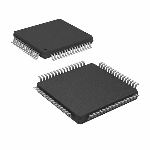
IDT821054A
64 Pin TQFP
1
2
3
4
5
6
7
8
9
10
11
12
13
14
15
16
49
50
51
52
53
54
55
56
57
58
59
60
61
62
63
64
SI2_3
SI1_3
SB3_3
SB2_3
SB1_3
SO2_3
SO1_3
SO1_4
SO2_4
SB1_4
SB2_4
SB3_4
SI1_4
SI2_4
INT34
CHCLK2
VIN1
GNDA1
VOUT1
VDDA12
VOUT2
GNDA2
VIN2
CNF
VDDB
VIN3
GNDA3
VOUT3
VDDA34
VOUT4
GNDA4
VIN4
2
32
31
30
29
28
27
26
25
24
23
22
21
20
19
18
17
BCLK
FS
DR2
DX2
TSX2
DR1
DX1
TSX1
VDDD
RESET
MCLK
GNDD
CO
CI
CCLK
CS
�IDT821054A QUAD PROGRAMMABLE PCM CODEC WITH MPI INTERFACE
INDUSTRIAL TEMPERATURE
TABLE OF CONTENTS
1
Pin Description...................................................................................................................................................................................................7
2
Functional Description ......................................................................................................................................................................................9
2.1 MPI/PCM Interface ....................................................................................................................................................................................9
2.1.1 Microprocessor Interface (MPI) ....................................................................................................................................................9
2.1.2 PCM Bus ....................................................................................................................................................................................10
2.2 DSP Programming...................................................................................................................................................................................11
2.2.1 Signal Processing.......................................................................................................................................................................11
2.2.2 Gain Adjustment.........................................................................................................................................................................11
2.2.3 Impedance Matching .................................................................................................................................................................11
2.2.4 Transhybrid Balance ..................................................................................................................................................................12
2.2.5 Frequency Response Correction................................................................................................................................................12
2.3 SLIC Control ............................................................................................................................................................................................12
2.3.1 SI1 and SI2.................................................................................................................................................................................12
2.3.2 SB1, SB2 and SB3 .....................................................................................................................................................................12
2.3.3 SO1 and SO2 .............................................................................................................................................................................12
2.4 Hardware Ring Trip .................................................................................................................................................................................12
2.5 Interrupt and Interrupt Enable..................................................................................................................................................................12
2.6 Debounce Filters .....................................................................................................................................................................................13
2.7 Chopper Clock.........................................................................................................................................................................................13
2.8 Dual Tone and Ring Generation..............................................................................................................................................................13
2.9 Level Metering .........................................................................................................................................................................................14
2.10 Channel Power Down/Standby Mode......................................................................................................................................................14
2.11 Power Down/Suspend Mode ...................................................................................................................................................................14
3
Operating The IDT821054A .............................................................................................................................................................................15
3.1 Programming Description ........................................................................................................................................................................15
3.1.1 Command Type and Format ......................................................................................................................................................15
3.1.2 Addressing the Local Registers..................................................................................................................................................15
3.1.3 Addressing the Global Registers................................................................................................................................................15
3.1.4 Addressing the Coe-RAM...........................................................................................................................................................15
3.1.5 Programming Examples .............................................................................................................................................................16
3.1.5.1 Example of Programming Local Registers .................................................................................................................16
3.1.5.2 Example of Programming Global Registers................................................................................................................16
3.1.5.3 Example of Programming the Coefficient-RAM..........................................................................................................16
3.2 Power-on Sequence ................................................................................................................................................................................19
3.3 Default State After Reset.........................................................................................................................................................................19
3.4 Registers Description ..............................................................................................................................................................................20
3.4.1 Registers Overview ....................................................................................................................................................................20
3.4.2 Global Registers List ..................................................................................................................................................................22
3.4.3 Local Registers List ....................................................................................................................................................................28
4
Absolute Maximum Ratings ............................................................................................................................................................................32
5
Recommended DC Operating Conditions .....................................................................................................................................................32
6
Electrical Characteristics ................................................................................................................................................................................32
6.1 Digital Interface........................................................................................................................................................................................32
6.2 Power Dissipation....................................................................................................................................................................................32
6.3 Analog Interface ......................................................................................................................................................................................33
7
Transmission Characteristics .........................................................................................................................................................................34
7.1 Absolute Gain ..........................................................................................................................................................................................34
7.2 Gain Tracking ..........................................................................................................................................................................................34
7.3 Frequency Response ..............................................................................................................................................................................34
7.4 Group Delay ............................................................................................................................................................................................35
7.5 Distortion .................................................................................................................................................................................................35
7.6 Noise .......................................................................................................................................................................................................36
3
�IDT821054A QUAD PROGRAMMABLE PCM CODEC WITH MPI INTERFACE
7.7
7.8
INDUSTRIAL TEMPERATURE
Interchannel Crosstalk.............................................................................................................................................................................36
Intrachannel Crosstalk.............................................................................................................................................................................36
8
Timing Characteristics ....................................................................................................................................................................................37
8.1 Clock Timing............................................................................................................................................................................................37
8.2 Microprocessor Interface Timing .............................................................................................................................................................38
8.3 PCM Interface Timing..............................................................................................................................................................................39
9
Appendix: IDT821054A Coe-RAM Mapping ...................................................................................................................................................40
10 Ordering Information .......................................................................................................................................................................................41
4
�IDT821054A QUAD PROGRAMMABLE PCM CODEC WITH MPI INTERFACE
INDUSTRIAL TEMPERATURE
LIST OF FIGURES
Figure - 1
Figure - 2
Figure - 3
Figure - 4
Figure - 5
Figure - 6
Figure - 7
Figure - 8
Figure - 9
Figure - 10
Figure - 11
An Example of the MPI Interface Write Operation .............................................................................................................................. 9
An Example of the MPI Interface Read Operation (ID = 81H)............................................................................................................. 9
Sampling Edge Selection Waveform................................................................................................................................................. 10
Signal Flow for Each Channel ........................................................................................................................................................... 11
Debounce Filter ................................................................................................................................................................................. 13
Clock Timing...................................................................................................................................................................................... 37
MPI Input Timing ............................................................................................................................................................................... 38
MPI Output Timing ............................................................................................................................................................................ 38
Transmit and Receive Timing............................................................................................................................................................ 39
Typical Frame Sync Timing (2 MHz Operation) ................................................................................................................................ 39
Coe-RAM Mapping............................................................................................................................................................................ 40
5
�IDT821054A QUAD PROGRAMMABLE PCM CODEC WITH MPI INTERFACE
INDUSTRIAL TEMPERATURE
LIST OF TABLES
Table - 1
Table - 2
Table - 3
Table - 4
Consecutive Adjacent Addressing......................................................................................................................................................15
Global Registers (GREG) Mapping ....................................................................................................................................................20
Local Registers (LREG) Mapping.......................................................................................................................................................21
Coe-RAM Address Allocation.............................................................................................................................................................40
6
�IDT821054A QUAD PROGRAMMABLE PCM CODEC WITH MPI INTERFACE
1
INDUSTRIAL TEMPERATURE
PIN DESCRIPTION
Name
Type
Pin Number
Description
GNDA1
GNDA2
GNDA3
GNDA4
Ground
50
54
59
63
Analog Ground.
All ground pins should be connected together.
GNDD
Ground
21
Digital Ground.
All digital signals are referred to this pin.
VDDA12
VDDA34
Power
52
61
+5 V Analog Power Supply.
These pins should be connected to ground via a 0.1 µF capacitor. All power supply pins should be
connected together.
VDDD
Power
24
+5 V Digital Power Supply.
VDDB
Power
57
+5 V Analog Power Supply.
This pin should be connected to ground via a 0.1 µF capacitor. All power supply pins should be connected
together.
CNF
−
56
Capacitor Noise Filter.
This pin should be connected to ground via a 0.22 µF capacitor.
VIN1-4
I
49, 55, 58, 64
Analog Voice Inputs of Channel 1-4.
These pins should be connected to the corresponding SLIC via a 0.22 µF capacitor.
VOUT1-4
O
51, 53, 60, 62
Voice Frequency Receiver Outputs of Channel 1-4.
These pins can drive 300 Ω AC load. It can drive transformers directly.
SI1_(1-4)
SI2_(1-4)
I
36, 47, 2, 13
SLIC Signalling Inputs with debounce function for Channel 1-4.
35, 48, 1, 14
SB1_(1-4)
SB2_(1-4)
SB3_(1-4)
I/O
39, 44, 5, 10
Bi-directional SLIC Signalling I/Os for Channel 1-4.
38, 45, 4, 11
These pins can be individually programmed as input or output.
37, 46, 3, 12
SO1_(1-4)
SO2_(1-4)
O
41, 42, 7, 8
SLIC Signalling Outputs for Channel 1-4.
40, 43, 6, 9
DX1
O
26
Transmit PCM Data Output, PCM Highway One.
Transmit PCM Data to PCM highway one. The PCM data is output through DX1 or DX2 as selected by
local register LREG5. This pin remains in high-impedance state until a pulse appears on the FS pin.
DX2
O
29
Transmit PCM Data Output, PCM Highway Two.
Transmit PCM Data to PCM highway two. The PCM data is output thought DX1 or DX2 as selected by
local register LREG5. This pin remains in high-impedance state until a pulse appears on the FS pin.
DR1
I
27
Receive PCM Data Input, PCM Highway One.
The PCM data is received from PCM highway one (DR1) or two (DR2). The receive PCM highway is
selected by local register LREG6.
DR2
I
30
Receive PCM Data Input, PCM Highway Two.
The PCM data is received from PCM highway one (DR1) or two (DR2). The receive PCM highway is
selected by local register LREG6.
FS
I
31
Frame Synchronization.
FS is an 8 kHz synchronization clock that identifies the beginning of the PCM frame.
BCLK
I
32
Bit Clock.
This pin clocks out the PCM data to DX1 or DX2 pin and clocks in PCM data from DR1 or DR2 pin. It may
vary from 512 kHz to 8.192 MHz and should be synchronous to FS.
7
�IDT821054A QUAD PROGRAMMABLE PCM CODEC WITH MPI INTERFACE
INDUSTRIAL TEMPERATURE
Name
Type
Pin Number
Description
TSX1
TSX2
0
25
28
Transmit Output Indicator.
The TSX1 pin becomes low when PCM data is transmitted via DX1. Open-drain.
The TSX2 pin becomes low when PCM data is transmitted via DX2. Open-drain.
CS
I
17
Chip Selection.
A logic low level on this pin enables the Serial Control Interface.
CI
I
19
Serial Control Interface Data Input.
Control data input pin. CCLK determines the data rate.
CO
O
20
Serial Control Interface Data Output.
Control data output pin. CCLK determines the data rate. This pin is in high-impedance state when the CS
pin is logic high.
CCLK
I
18
Serial Control Interface Clock.
This is the clock for the Serial Control Interface. It can be up to 8.192 MHz.
MCLK
I
22
Master Clock Input.
This pin provides the clock for the DSP of the IDT821054A. The frequency of the MCLK can be 1.536
MHz, 1.544 MHz, 2.048 MHz, 3.072 MHz, 3.088 MHz, 4.096 MHz, 6.144 MHz, 6.176 MHz or 8.192 MHz.
RESET
I
23
Reset Input.
Forces the device to default mode. Active low.
INT12
O
34
Interrupt Output Pin for Channel 1-2.
Active high interrupt signal for Channel 1 and 2, open-drain. It reflects the changes on the corresponding
SLIC input pins.
INT34
O
15
Interrupt Output Pin for Channel 3-4.
Active high interrupt signal for Channel 3 and 4, open-drain. It reflects the changes on the corresponding
SLIC input pins.
CHCLK1
O
33
Chopper Clock Output One.
Provides a programmable output signal (2 -28 ms) synchronous to MCLK.
CHCLK2
O
16
Chopper Clock Output Two.
Provides a programmable output signal (256 kHz, 512 kHz or 16.384 MHz) synchronous to MCLK.
8
�IDT821054A QUAD PROGRAMMABLE PCM CODEC WITH MPI INTERFACE
2
FUNCTIONAL DESCRIPTION
interface and the Coefficient-RAM of the IDT821054A are programmed
by the master device via MPI, which consists of four lines (pins): CCLK,
CS, CI and CO. All commands and data are aligned in byte (8 bits) and
transferred via the MPI interface. CCLK is the clock of the MPI interface.
The frequency of CCLK can be up to 8.192 MHz. CS is the chip
selection pin. A low level on CS enables the MPI interface. CI and CO
are data input and data output pins, carrying control commands and
data bytes to/from the IDT821054A.
The data transfer is synchronized to the CCLK signal. The contents
of CI is latched on the rising edges of CCLK, while CO changes on the
falling edges of CCLK. The CCLK signal is the only reference of CI and
CO pins. Its duty and frequency may not necessarily be standard.
When the CS pin becomes low, the IDT821054A treats the first byte
on the CI pin as command and the rest as data. To write another
command, the CS pin must be changed from low to high to finish the
previous command and then changed from high to low to indicate the
start of a new command. When a read/write operation is completed, the
CS pin must be set to high in 8-bit time.
During the execution of commands that are followed by output data
byte(s), the IDT821054A will not accept any new commands from the CI
pin. But the data transfer sequence can be interrupted by setting the CS
pin to high at any time. See Figure - 1 and Figure - 2 for examples of
MPI write and read operation timing diagrams.
The IDT821054A is a four-channel PCM CODEC with on-chip digital
filters. It provides a four-wire solution for the subscriber line circuitry in
digital switches. The IDT821054A converts analog voice signals to
digital PCM samples and digital PCM samples back to analog voice
signals. The digital filters are used to bandlimit the voice signals during
conversion. High performance oversampling Analog-to-Digital
Converters (ADC) and Digital-to-Analog Converters (DAC) in the
IDT821054A provide the required conversion accuracy. The associated
decimation and interpolation filtering is performed by both dedicated
hardware and Digital Signal Processor (DSP). The DSP also handles all
other necessary procession such as PCM bandpass filtering, sample
rate conversion and PCM companding.
2.1
MPI/PCM INTERFACE
A serial Microprocessor Interface (MPI) is provided for the master
device to control the IDT821054A. Two PCM buses are provided to
transfer the digital voice data.
2.1.1
INDUSTRIAL TEMPERATURE
MICROPROCESSOR INTERFACE (MPI)
The internal configuration registers (local/global), the SLIC signaling
CCLK
CS
CI
7
6
5
4
3
2
1
0
7
6
5
Command Byte
CO
4
3
2
1
0
7
6
5
Data Byte 1
4
3
2
1
0
2
1
0
Data Byte 2
High 'Z'
Figure - 1 An Example of the MPI Interface Write Operation
CCLK
CS
Ignored
CI
7
6
5
4
3
2
1
0
Command Byte
CO
High 'Z'
Identification Code
'1'
'0'
'0'
'0'
'0'
'0'
Data Byte 1
'0'
'1'
7
6
Figure - 2 An Example of the MPI Interface Read Operation (ID = 81H)
9
5
4
3
�IDT821054A QUAD PROGRAMMABLE PCM CODEC WITH MPI INTERFACE
2.1.2
INDUSTRIAL TEMPERATURE
complement number (b13 to b0 are effective bits, b15 and b14 are as
same as the sign bit b13). So, the voice data of one channel occupies
one time slot group, which consists of 2 adjacent time slots. The TT[6:0]
bits in LREG5 select a transmit time slot group for the specified channel.
If TT[6:0] = n(d), it means that time slots TS(2n+1) and TS(2n+2) are
selected. For example, if TT[6:0] = 00H, it means that TS0 and TS1 are
selected. The RT[6:0] bits in LREG6 select a receive time slot group for
the specified channel in the same way.
The PCM data of each individual channel can be clocked out to
transmit PCM highway one (DX1) or two (DX2) on the programmed
edges of BCLK according to time slot assignment. The transmit PCM
highway is selected by the THS bit in LREG5. The frame sync (FS)
pulse identifies the beginning of a transmit frame (TS0). The PCM data
is serially transmitted on DX1 or DX2 with MSB first.
The PCM data of each individual channel is received from receive
PCM highway one (DR1) or two (DR2) on the programmed edges of
BCLK according to time slot assignment. The receive PCM highway is
selected by the RHS bit in LREG6. The frame sync (FS) pulse identifies
the beginning of a receive frame (TS0). The PCM data is serially
received from DR1 or DR2 with MSB first.
PCM BUS
The IDT821054A provides two flexible PCM buses for all 4 channels.
The digital PCM data can be compressed (A/µ-law) or linear code. As
shown in Figure - 3, the data rate can be configured as same as the Bit
Clock (BCLK) or half of it. The PCM data is transmitted or received
either on the rising edges or on the falling edges of the BCLK signal. The
transmit and receive time slots can offset from the FS signal by 0 to 7
periods of BCLK. All these configurations are made by global register
GREG7, which is effective for all four channels.
The PCM data of each channel can be assigned to any time slot of
the PCM bus. The number of available time slots is determined by the
frequency of the BCLK signal. For example, if the frequency is 512 kHz,
8 time slots (TS0 to TS7) are available. If the frequency is 1.024 MHz,
16 time slots (TS0 to TS15) are available. The IDT821054A accepts
BCLK frequency of 512 kHz to 8.192 MHz at increments of 64 kHz.
When compressed PCM code (8-bit wide) is selected, the voice data
of one channel occupies one time slot. The TT[6:0] bits in local register
LREG5 select the transmit time slot for each channel, while the RT[6:0]
bits in LREG6 select the receive time slot for each channel.
When linear PCM code is selected, the voice data is a 16-bit 2’s
Transmit
Receive
FS
PCM Clock Slope Bits
in GREG7:
BCLK
Single Clock
CS = 000
CS = 001
CS = 010
CS = 011
Bit 7
TS0
BCLK
Double Clock
CS = 100
CS = 101
CS = 110
CS = 111
Figure - 3 Sampling Edge Selection Waveform
10
�IDT821054A QUAD PROGRAMMABLE PCM CODEC WITH MPI INTERFACE
2.2
DSP PROGRAMMING
2.2.1
SIGNAL PROCESSING
INDUSTRIAL TEMPERATURE
impedance, balance transhybrid and correct frequency response. All the
coefficients of the digital filters can be calculated automatically by a
software provided by IDT. When users provide accurate SLIC model,
impedance and gain requirements, this software will calculate all the
coefficients automatically. After loading these coefficients to the
coefficient RAM of the IDT821054A, the final AC characteristics of the
line card (consists of SLIC and CODEC) will meet the ITU-T
specifications.
Several blocks are programmable for signal processing. This allows
users to optimize the performance of the IDT821054A for the system.
Figure - 4 shows the signal flow for each channel and indicates the
programmable blocks.
The programmable digital filters are used to adjust gain and
LREG1: CS[3]
CS[3] = 1: enable (normal)
CS[3] = 0: disable (bypass)
Transmit Path
Analog
@64 KHz
@2 MHz
@8 KHz
@16 KHz
TS
PCM Highway
Level Meter
VIN
LPF/AA
UF
GRX
U2
FRX
HPF
CMP
ECF
LPF
FRR
EXP
Dual Tone
LREG1: CS[2]
CS[2] = 1: enable (normal)
CS[2] = 0: disable (cut)
LREG1: CS[0]
CS[0] = 1: enable (normal)
CS[0] = 0: disable (cut)
TSA
DX1/DX2
ALB-DI
U1
LPF
DLB-DI
∑ −∆
IMF
D2
DLB-PCM
LPF/SC
GIS
GTX
DLB-8K
ALB-8K
ALB-1BIT
DLB_1BIT
DLB-ANA
VOUT
D1
∑ −∆
TSA
DR1/DR2
CUT-OFF-PCM
LREG1: CS[1]
CS[1] = 1: enable (normal)
CS[1] = 0: disable (cut)
Bold Black Framed: Programmable Filters
Receive Path
Fine Black Framed: Fixed Filters
Figure - 4 Signal Flow for Each Channel
Abbreviation List:
LPF/AA: Anti-Alias Low-pass Filter
LPF/SC: Smoothing Low-pass Filter
LPF: Low-pass Filter
HPF: High-pass Filter
GIS: Gain for Impedance Scaling
D1: 1st Down Sample Stage
D2: 2nd Down Sample Stage
U1: 1st Up Sample Stage
U2: 2nd Up Sample Stage
UF: Up Sampling Filter (64 k - 128 k)
2.2.2
IMF: Impedance Matching Filter
ECF: Echo Cancellation Filter
GTX: Gain for Transmit Path
GRX: Gain for Receive Path
FRX: Frequency Response Correction for Transmit
FRR: Frequency Response Correction for Receive
CMP: Compression
EXP: Expansion
TSA: Time Slot Assignment
minimum 0.1 dB step.
For each channel, the digital gain filter in the receive path (GRX) can
be disabled by setting the CS[7] bit in LREG1 to ‘0’. If the CS[7] bit in
LREG1 is set to ‘1’, the GRX filter will be enabled and the digital gain will
be programmed by the coefficient RAM. Note that the RAM block for
containing GRX coefficient is shared by all four channels. That is, once
the GRX coefficient is written to the coe-RAM, it will be used by all four
channels. The GRX is programmable from -12 dB to +3 dB with
minimum 0.1 dB step.
GAIN ADJUSTMENT
For each individual channel, the analog A/D gain in the transmit path
can be selected as 0 dB or 6 dB. The selection is done by the GAD bit in
LREG9. It is 0 dB by default.
For each individual channel, the analog D/A gain in the receive path
can be selected as 0 dB or -6 dB. The selection is done by the GDA bit
in LREG9. It is 0 dB by default.
For each channel, the digital gain filter in the transmit path (GTX) can
be disabled by setting the CS[5] bit in LREG1 to ‘0’. If the CS[5] bit in
LREG1 is set to ‘1’, the GTX filter will be enabled and the digital gain will
be programmed by the coefficient RAM. Note that the RAM block for
containing GTX coefficient is shared by all four channels. That is, once
the GTX coefficient is written to the coe-RAM, it will be used by all four
channels. The GTX is programmable from -3 dB to +12 dB with
2.2.3
IMPEDANCE MATCHING
The IDT821054A provides a programmable feedback path from VIN
to VOUT for each channel. This feedback synthesizes the two-wire
impedance of the SLIC. The programmable Impedance Matching Filter
11
�IDT821054A QUAD PROGRAMMABLE PCM CODEC WITH MPI INTERFACE
channels. Users can also read the information of SB1, SB2 and SB3 of
the specified channel from local register LREG4.
If the SB1, SB2 and SB3 pins are configured as outputs, data can
only be written to them via GREG10, GREG11 and GREG12
respectively.
(IMF) and Gain of Impedance Scaling filter (GIS) work together to realize
impedance matching. If the CS[0] bit in LREG1 is ‘0’, the IMF is
disabled. If the CS[0] bit is ‘1’, the IMF coefficient is programmed by the
coefficient RAM. If the CS[2] bit in LREG1 is ‘0’, the GIS filter is disabled.
If the CS[2] bit is ‘1’, the GIS coefficient is programmed by the coefficient
RAM.
2.3.3
2.2.4
TRANSHYBRID BALANCE
2.4
FREQUENCY RESPONSE CORRECTION
SLIC CONTROL
The SLIC control interface of the IDT821054A consists of 7 pins per
channel: 2 inputs SI1 and SI2, 3 I/Os SB1 to SB3, and 2 outputs SO1
and SO2.
2.3.1
SI1 AND SI2
The SLIC inputs SI1 and SI2 can be read in 2 ways - globally for all 4
channels or locally for each individual channel.
The SI1 and SI2 status of all 4 channels can be read via global
register GREG9. The SIA[3:0] bits in this register represent the
debounced SI1 data of Channel 4 to Channel 1. The SIB[3:0] bits in this
register represent the debounced SI2 data of Channel 4 to Channel 1.
Both the SI1 and SI2 pins can be connected to off-hook, ring trip,
ground key signals or other signals. The global register GREG9
provides a more efficient way to obtain time-critical data such as on/offhook and ring trip information from the SLIC input pins SI1 and SI2.
The SI1 and SI2 status of each channel can also be read via the
corresponding local register LREG4.
2.3.2
HARDWARE RING TRIP
In order to avoid the damage caused by high voltage ring signal, the
IDT821054A provides a hardware ring trip function to respond to the offhook signal as fast as possible. This function is enabled by setting the
RTE bit in GREG8 to ‘1’.
The off-hook signal can be input via either SI1 or SI2 pin, while the
ring control signal can be output via any of the SO1, SO2, SB1, SB2 and
SB3 pins (assume that SB1-SB3 are configured as outputs). The IS bit
in GREG8 is used to select an input pin and the OS[2:0] bits are used to
select an output pin.
When a valid off-hook signal arrives at the selected input pin (SI1 or
SI2), the IDT821054A will turn off the ring signal by inverting the logic
level of the selected output pin (SO1, SO2, SB1, SB2 or SB3),
regardless of the value of the corresponding SLIC output control register
(the value should be changed later). This function provides a much
faster response to off-hook signals than the software ring trip which
turns off the ring signal by changing the value of the corresponding
register.
The IPI bit in GREG8 is used to indicate the valid polarity of the input
pin. If the off-hook signal is active low, the IPI bit should be set to ‘0’. If
the off-hook signal is active high, the IPI bit should be set to ‘1’. The OPI
bit in GREG8 is used to indicate the valid polarity of the output pin. If the
ring control signal is required to be low in normal status and high to
activate a ring, the OPI bit should be set to ‘1’. If it is required to be high
in normal status and low to activate a ring, the OPI bit should be set to
‘0’.
Here is an example: In a system where the off-hook signal is active
low and ring control signal is active high, the IPI bit should be set to ‘0’
and the OPI bit should be set to ‘1’. In normal status, the selected input
(off-hook signal) is high and the selected output (ring control signal) is
low. When the ring is activated by setting the output (ring control signal)
to high, a low pulse appearing on the input (off-hook signal) will inform
the device to invert the output to low and cut off the ring signal.
The IDT821054A provides two filters that can be programmed to
correct any frequency distortion caused by the impedance matching
filter. They are the Frequency Response Correction in the Transmit path
filter (FRX) and the Frequency Response Correction in the Receive path
filter (FRR). If the CS[4] bit in LREG1 is ‘0’, the FRX filter is disabled. If
the CS[4] bit is ‘1’, the FRX coefficient is programmed by the coefficient
RAM. If the CS[6] bit in LREG1 is ‘0’, the FRR filter is disabled. If the
CS[6] bit is ‘1’, the FRR coefficient is programmed by the coefficient
RAM.
Refer to “9 Appendix: IDT821054A Coe-RAM Mapping” for the
address of the GTX, GRX, FRX, FRR, GIS, ECF and IMF coefficients.
2.3
SO1 AND SO2
The control data can only be written to the two output pins SO1 and
SO2 by local register LREG4 on a per-channel basis. When being read,
the SO1 and SO2 bits in LREG4 will be read out with the data written to
them in the previous write operation.
The ECF filter is used to adjust transhybrid balance and ensure that
the echo cancellation meets the ITU-T specifications. If the CS[1] bit in
LREG1 is ‘0’, the ECF filter is disabled. If the CS[1] bit is ‘1’, the ECF
coefficient is programmed by the coefficient RAM.
2.2.5
INDUSTRIAL TEMPERATURE
SB1, SB2 AND SB3
2.5
The SLIC I/O pin SB1 of each channel can be configured as input or
output via global register GREG10. The SB1C[3:0] bits in GREG10
determine the SB1 directions of Channel 4 to Channel 1: ‘0’ means input
and '1' means output. The SB2C[3:0] bits in GREG11 and the SB3C[3:0]
bits in GREG12 respectively determine the SB2 and SB3 directions of
Channel 4 to Channel 1 in the same way.
If the SB1, SB2 or SB3 pin is selected as input, its information can be
read from both global and local registers. The SB1[3:0], SB2[3:0] and
SB3[3:0] bits in global registers GREG10, GREG11 and GREG12
respectively contain the information of SB1, SB2 and SB3 for all four
INTERRUPT AND INTERRUPT ENABLE
An interrupt mechanism is provided in the IDT821054A for reading
the SLIC input state. Each change of the SLIC input state will generate
an interrupt.
Any of the SLIC inputs including SI1, SI2, SB1, SB2 and SB3 (if SB1SB3 are configured as inputs) can be an interrupt source. As SI1 and
SI2 signals are debounced while the SB1 to SB3 signals are not, users
should pay more attention to the interrupt sources of SB1 to SB3.
Local register LREG2 is used to enable/disable the interrupts. Each
bit of IE[4:0] in LREG2 corresponds to one interrupt source of the
12
�IDT821054A QUAD PROGRAMMABLE PCM CODEC WITH MPI INTERFACE
initially clocked at half of the frame sync rate (250 µs). Any data
changing at this sample rate resets a counter that clocks at the rate of 2
ms. The value of the counter is programmable from 0 to 30 via LREG3.
The debounced SI1 signals of Channel 4 to 1 are written to the SIA[3:0]
bits in GREG9. The corresponding SIA bit will not be updated until the
value of the counter is reached. The SI1 pin usually contains the SLIC
switch hook status.
The GK[3:0] bits in LREG3 are used to program the debounce
interval of the SI2 input of the corresponding channel. The debounced
SI2 signals of Channel 4 to 1 are written to the SIB[3:0] bits in GREG9.
The GK debounce filter consists of a six-state up/down counter that
ranges between 0 and 6. This counter is clocked by the GK timer at the
sampling period of 0-30 ms, which is programmed via LREG3. If the
sampled value is low, the value of the counter will be decremented by
each clock pulse. If the sampled value is high, the value of the counter is
incremented by each clock pulse. When the value increases to 6, it sets
a latch whose output is routed to the corresponding SIB bit. If the value
decreases to 0, the latch will be cleared and the output bit will be set to
0. In other cases, the latch and the SIB status remain in their previous
state without being changed. In this way, at least six consecutive GK
clocks with the debounce input remaining at the same state can effect
an output change.
specified channel. When one bit of IE[4:0] is ‘0’, the corresponding
interrupt is ignored (disabled), otherwise, the corresponding interrupt is
recognized (enabled).
Multiple interrupt sources can be enabled at the same time. All
interrupts can be cleared simultaneously by executing a write operation
to global register GREG2. Additionally, the interrupts caused by all four
channels’ SI1 and SI2 status changes can be cleared by applying a read
operation to GREG9. If SB1, SB2 and SB3 pins are configured as
inputs, a read operation to GREG10, GREG11 and GREG12 clears the
interrupt generated by the corresponding SB port of all four channels. A
read operation to LREG4 clears all 7 interrupt sources of the specified
channel.
2.6
DEBOUNCE FILTERS
For each channel, the IDT821054A provides two debounce filter
circuits: Debounced Switch Hook (DSH) Filter for the SI1 signal and
Ground Key (GK) Filter for the SI2 signal. See Figure - 5 for details. The
two debounce filters are used to buffer the input signals on SI1 and SI2
pins before changing the state of the SLIC Debounced Input SI1/SI2
Register (GREG9). The Frame Sync (FS) signal is necessary for both
DSH and GK filters.
The DSH[3:0] bits in LREG3 are used to program the debounce
period of the SI1 input of the corresponding channel. The DSH filter is
SI1
D
Q
D
INDUSTRIAL TEMPERATURE
Q
D
Q
D
Q
SIA
E
DSH[3:0]
Debounce
Period
(0-30 ms)
FS/2
4 kHz
=0
≠0
SI2
GK[3:0]
Debounce
Interval
(0-30 ms)
D
Q
7 bit Debounce
Counter
up/
Q
down
D
Q
RST
7 bit Debounce
Counter
SIB
GK
6 states
Up/down
Counter
Figure - 5 Debounce Filter
2.7
CHOPPER CLOCK
and tone generator 1) for each channel. They can produce signals such
as test tone, DTMF, dial tone, busy tone, congestion tone and Caller-ID
Alerting Tone, and output it to the VOUT pin.
The dual tone generators of each channel can be enabled by setting
the TEN0 and TEN1 bits in LREG10 to ‘1’respectively.
The frequency and amplitude of the tone signal are programmed by
the Coe-RAM. The frequency and amplitude coefficients are calculated
by the following formulas:
Frequency coefficient = 32767∗ cos(f / 8000 ∗ 2 ∗ π)
Amplitude coefficient = A ∗ 32767 ∗ sin(f / 8000 ∗ 2 ∗ π)
Herein, 'f' is the desired frequency of the tone signal, 'A' is the scaling
parameter of the amplitude. The range of 'A' is from 0 to 1.
A = 1, corresponds to the maximum amplitude of 1.57 V.
The IDT821054A provides two programmable chopper clock outputs
CHCLK1 and CHCLK2. They can be used to drive the power supply
switching regulators on SLICs. The two chopper clocks are synchronous
to MCLK. The CHCLK1 outputs a signal which clock cycle is
programmable from 2 to 28 ms. The CHCLK2 outputs a signal which
frequency can be 256 kHz, 512 kHz or 16.384 MHz. The frequencies of
the two chopper clocks are programmed by global register GREG5.
2.8
DUAL TONE AND RING GENERATION
The IDT821054A provides two tone generators (tone generator 0
13
�IDT821054A QUAD PROGRAMMABLE PCM CODEC WITH MPI INTERFACE
INDUSTRIAL TEMPERATURE
A = 0, corresponds to the minimum amplitude of 0 V.
It is a linear relationship between 'A' and the amplitude. That is, if
A=β ( 0